

IV/IV B.Tech DEGREE EXAMINATION
October,2016 EIE
Seventh Semister VLSI design(EI 412)
Scheme of Evaluation
1. 12X1=12M
(a) Figure of merit is a measure for frequency response and switching performance of a MOS
transistor .Figure of merit is defined as :
ω� =��
�� where gm is trans conductance.
Cg is gate capacitance.
(b) Latchup refers to short circuit formed between power and ground rails in an IC leading
to high current and damage to the IC. Speaking about CMOS transistors, latch up is the
phenomenon of low impedance path between power rail and ground rail due to interaction
between parasitic pnp and npn transistors.
(c) A positive resist is a type of photoresist in which the portion of the photoresist that is exposed to light becomes soluble to the photoresist developer. The portion of the photoresist that is unexposed remains insoluble to the photoresist developer.
A negative resist is a type of photoresist in which the portion of the photoresist that is exposed to light becomes insoluble to the photoresist developer. The unexposed portion of the photoresist is dissolved by the photoresist developer.
(d) MOS circuits are formed on four basic layers-n-diffusion diffusion, p-diffusiqn diffusiqn,
polysilicon, and metal, which are isolated from one another another by thick or thin (thinox)
silicon silicon dioxide insulating layers.
(e) CMOS Device Scaling
Parameters Variables Scaling Factor
Dimensions W,L,xox
,xj 1/
Potentials Vds
,Vgs
1/k
Doping Concentration N
2
/k
Electric Field E /k
Current Ids
/k
2
Gate Delay T k/
2
=dimensional scaling factor
k=supply voltage scaling factor
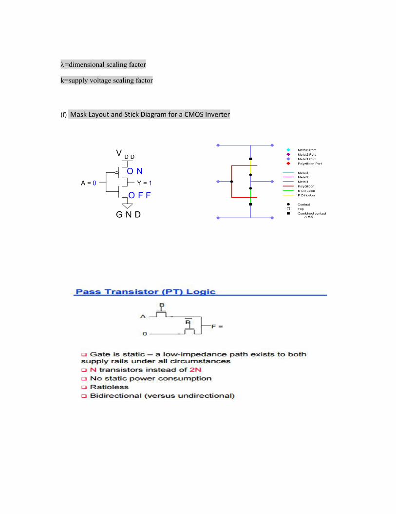
(f) Mask Layout and Stick Diagram for a CMOS Inverter
VD D
A = 0 Y = 1
G N D
O F F
O N

(g)
(h) Manchester carry – chain This implementation can be very performant (20 transistors)
depending on the way the XOR function is built. The carry propagation of the carry is
controlled by the output of the XOR gate. The generation of the carry is directly made by the
function at the bottom. When both input signals are 1, then the inverse output carry is 0.
A
B
A
B
B B B B
A
B
A
B
F=AB
F = AB
F=A+B
F = A+B
B B
A
A
A
A
F=A Ý
F = A Ý
OR/NOR EXOR/NEXOR AND/NAND
F
F
Pass-Transistor
Network
Pass-Trsr
Network
A A BB
A A BB
In
(a)
(b)

The carry passes through a complete transmission gate. If the carry path is precharged to
VDD, the transmission gate is then reduced to a simple NMOS transistor. In the same way
the PMOS transistors of the carry generation is removed. One gets a Manchester cell.
(i) Transmission gates represent another class of logic circuits, which use
Transmission gates as basic building block. A transmission gate consist of a
PMOS and NMOS connected in parallel. Gate voltage applied to these gates is
complementary of each other (C and Cbar shown in figure 1). Transmission
gates act as bidirectional switch between two nodes A and B controlled by
signal C. Gate of NMOS is connected to C and gate of PMOS is connected to
Cbar(invert of C). When control signal C is high i.e. VDD, both transistor are on
and provides a low resistance path between A and B. On the other hand,
when C is low, both transistors are turned off and provide high impedance
path between A and B.
(j) FPGA vs ASIC
Speed
ASIC rules out FPGA in terms of speed. As ASIC are designed for a specific application they can be
optimized to maximum, hence we can have high speed in ASIC designs. ASIC can have hight speed
clocks.
Cost
FPGAs are cost effective for small applications. But when it comes to complex and large volume
designs (like 32-bit processors) ASIC products are cheaper.
Size/Area
FPGA are contains lots of LUTs, and routing channels which are connected via bit
streams(program). As they are made for general purpose and because of re-usability. They are in-
general larger designs than corresponding ASIC design. For example, LUT gives you both registered
and non-register output, but if we require only non-registered output, then its a waste of having a
extra circuitry. In this way ASIC will be smaller in size.

Power
FPGA designs consume more power than ASIC designs. As explained above the unwanted
circuitry results wastage of power. FPGA wont allow us to have better power optimization.
When it comes to ASIC designs we can optimize them to the fullest.
(k) Synthesis is the process of translating a design description to another level of abstraction, i.e, from behaviour to structure. We achieved synthesis by using a Synthesis tool like Foundation Express which outputs a netlist. It is similar to the compilation of a high level programming language like C into assembly code.
(l) The Bit type is an idealized value. type Bit is ('0', '1'); std_logic is part of the
std_logic_1164 package and provides more realistic modeling of signals within a digital
system.
UNIT-I
2.(a) 6M
Introduction about NMOSFET ----2M Various steps involved in the fabrication of NMOSFET ----4M There are a large number and variety of basic fabrication steps used in the production of modern MOS ICs. The same process can be used for the designed of NMOS or PMOS or CMOS devices.The gate material could be either metal or poly-silicon . The most commonly used substrate is bulk silicon or silicon-on-sapphire (SOS). Inorder to avoid the presence of parasitic transistors, variations are brought in the techniques that are used to isolate the devices in the wafer. The fabrication steps are as follows: Step1: Processing is carried on single crystal silicon of high purity on which required P impurities are introduced as crystal is grown. Such wafers are about 75 to 150 mm in diameter and 0.4 mm thick and they are doped with say boron to impurity concentration of 10 to power 15/cm3 to 10 to the power 16 /cm3.
Step 2 :

A layer of silicon di oxide (SiO2) typically 1 micrometer thick is grown all over the surface of the wafer to protect the surface, acts as a barrier to the dopant during processing, and provide a generally insulating substrate on to which other layers may be deposited and patterned.
Step 3: The surface is now covered with the photo resist which is deposited onto the wafer and spun to an even distribution of the required thickness.
Step 4: The photo resist layer is then exposed to ultraviolet light through masking which defines those regions into which diffusion is to take place together with transistor channels. Assume, for example , that those areas exposed to uv radiations are polymerized (hardened), but that the areas required for diffusion are shielded by the mask and remain unaffected.
Step 5: These areas are subsequently readily etched away together with the underlying silicon di oxide so that the wafer surface is exposed in the window defined by the mask.
Step 6: The remaining photo resist is removed and a thin layer of SiO2 (0.1 micro m typical) is grown over the entire chip surface and then poly silicon is deposited on the top of this to form the gate structure. The polysilicon layer consists of heavily doped polysilicon deposited by chemical vapour deposition (CVD). In the fabrication of fine pattern devices, precise control of thickness, impurity concentration, and resistivity is necessary
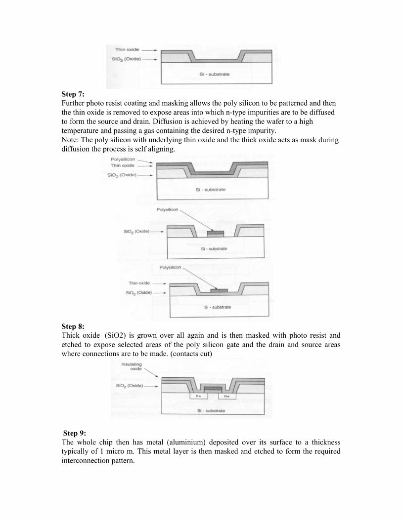
Step 7: Further photo resist coating and masking allows the poly silicon to be patterned and then the thin oxide is removed to expose areas into which n-type impurities are to be diffused to form the source and drain. Diffusion is achieved by heating the wafer to a high temperature and passing a gas containing the desired n-type impurity. Note: The poly silicon with underlying thin oxide and the thick oxide acts as mask during diffusion the process is self aligning.
Step 8: Thick oxide (SiO2) is grown over all again and is then masked with photo resist and etched to expose selected areas of the poly silicon gate and the drain and source areas where connections are to be made. (contacts cut)
Step 9: The whole chip then has metal (aluminium) deposited over its surface to a thickness typically of 1 micro m. This metal layer is then masked and etched to form the required interconnection pattern.

2.(b). 6M
Comparison between CMOS and Bipolar technologies ----- 6M
CMOS BIPOLAR
Low power dissipation High power dissipation Low current drive High current drive High input impedance Low input impedance High noise margin Medium noise margin Medium speed of operation
High speed of operation
High voltage swing Low voltage swing High packing density Low packing density High delay sensitivity Low delay sensitivity Low output drive High output drive
(OR)
3.(a) 6M
Introduction about Ids and V ds ----2M Derivation ----4M


3.(b). 6M
gm formula ----2M
Solution ----4M
gm = µnCox (W/ L) (Vgs − Vth)
=92.10.(1.2-0.8)
=368 A/V
UNIT-II
4. (a) 6M
Introduction about NMOS inverter ----2M Stick diagram ----4M
Stick Diagrams(NMOS): Basic Steps Normally,
the first step is to draw two parallel metal (blue) VDD and GND rails.
There should be enough space between them for other circuit elements.
Next, Active (Green) paths must be drawn for required transistors.

Do not forget to mark contacts as X, wherever required.
Remember, Poly (Red) crosses Active (Green/yellow), where transistor is required.
For depletion mode FET, draw required implants (yellow). Label each transistor with L:W
ratio.
Enhancement-Mode MOSFETs act as switches.
They are switched OFF, when the input to gate is low. So, they can be used to pull the
output down. Now, for pull-up, we can use a resistor. But resistors consume larger area.
Another alternative is using MOSFET as pull-up. The pull-up MOSFET can be
Enhancement-mode or Depletion mode. Enhancement-mode as pull-up: To use
Enhancement-mode FET as active load, the gate should be connected to a separate gate bias
voltage. Vo(max) = VDD – Vth.
Depletion mode as pull-up: Depletion-Mode FET has a channel with zero gate-bias. They
will not turn-off until sufficient reverse bias is applied to its gate. To be used as a load, the
gate should be connected to source. Vo(max) = VDD.

4 .(b). 6M
Layout design rules ----2M
Explanation ----4M
Types of Design Rules
The design rules primary address two issues:
1. The geometrical reproduction of features that can be reproduced by the maskmaking
and lithographical process ,and 2. The interaction between different layers.
There are primarily two approaches in describing the design rules.
1. Linear scaling is possible only over a limited range of dimensions.
2. Scalable design rules are conservative .This results in over dimensioned and less
dense design.
3. This rule is not used in real life.
1. Scalable Design Rules (e.g. SCMOS, λ-based design rules): In this approach, all
rules are defined in terms of a single parameter λ. The rules are so chosen that a
design can be easily ported over a cross section of industrial process ,making the
layout portable .Scaling can be easily done by simply changing the value of. The key
disadvantages of this approach are:
2. Absolute Design Rules (e.g. μ-based design rules ) : In this approach, the design
rules are expressed in absolute dimensions (e.g. 0.75μm) and therefore can exploit the
features of a given process to a maximum degree. Here, scaling and porting is more
demanding, and has to be performed either manually or using CAD tools .Also, these
rules tend to be more complex especially for deep submicron. The fundamental unity
in the definition of a set of design rules is the minimum line width .It stands for the
minimum mask dimension that can be safely transferred to the semiconductor
material .Even for the same minimum dimension, design rules tend to differ from
company to company, and from process to process. Now, CAD tools allow designs to
migrate between compatible processes.
(OR)
5.(a) 6M
Diagram ----2M
Explanation ----4M
For driving large load capacitance CL, can use N buffer drivers in series, each with
stage ratio Cout/Cin = a
– Input capacitance Cg
– Delay per stage = atd given that the delay of a minimum size stage driving
another minimum size stage is td

– Let R = CL/Cg = aN
– Then the total stage delay is given by Total Delay = Natd = atd(ln R/ ln a)
– Setting derivative of total delay w/r a equal to zero yields optimum stage ratio
a = e
• If we allow inclusion of inverter output drain capacitance term in the analysis, the
optimum stage ratio is given by aopt = e(k + aopt)/aopt where k = Cdrain/Cgate
5. (b). 6M
Introduction about wiring capacitance ----2M Sources of wiring capacitances ----4M
Wiring Capacitance:
The wiring capacitance depends upon the length and width of the connecting wires and is a
function of the fan-out from the driving gate and the number of fan-out gates. Wiring
capacitance is growing in importance with the scaling of technology. An extraction tool is
often used to determine the capacitance.

Fringe capacitance:
Width/Height ratio is now less than 1 to reduce resistance of wires Fringe capacitance:
Capacitance between sidewall and underlying substrate

UNIT-III
6.(a). 6M
Concept of Carry Look Ahead Adder ---- 2M
Design approach ---- 4M
Carry look ahead adder definition: Carry Look Ahead Adder (CLA Adder) (also known as
Carry Look Ahead Generator) is one of the digital circuits used to implement addition of
binary numbers. It is an improvement over 'Ripple carry adder' circuit. In Ripple Carry
adders, carry propagation time is the major speed limiting factor as it works on the basic
mechanism to generate carries as we generally do while adding two numbers using pen and
paper. A ripple carry adder may be supposed to be built of a series of 1-bit adders (generally
known as a full adder in digital electronics). Thus, the speed of ripple carry adder is a direct
function of number of bits. On the other hand, Carry Look Ahead adder solves this problem
by calculating carry signals in advance based upon input bits and does not wait for the input
signal to propagate through different adder stages. Hence, it implements the adder with
reduced delay at the cost of more area (as large combinational logic is required to calculate
the look ahead carry as compared to propagated carry).

6.(b). 6M
Introduction to subsystem ----2M
Pipelining relevant to subsystem ----4M
A data path is a logical and a physical structure:
– bitwise logical organization;
– bitwise physical design.
Datapath often has ALU, registers, some other function units.
Data is generally passed via busses.


Slice includes one bit of function units, connected by busses:
Many arithmetic and logical functions can be defined recursively on bits
of word.
A bit-slice is a one-bit (or n-bit) segment of an operation of minimum
size to ensure regularity.
Regular logical structure allows regular physical structure.
Cells in bit-slice may be abutted together -requires matching positions
on terminals.
Pitch-matching is designing cells to ensure that pins are at proper
positions for abuttin
A wiring plan shows layer assignments and directions for major signals.
Put most important signals on lowest-impedance, accessible layers.
Cannot support full connectivity between all data path elements - must
choose number of transfers per cycle allowed.

A bus circuit is a specialized multiplexer circuit.
Two major choices: pseudo-nMOS, precharged.
Pseudo-nMOS bus circuit
Precharged bus circuit
(OR)
7.(a) 6M

Introduction to multiplier ---2M
Braun multiplier ---4M
BRAUN MULTIPLIER The simplest parallel multiplier is the Braun array. All the partial
products are computed in parallel, then collected through a cascade of Carry Save Adders.
The completion time is limited by the depth of the carry save array, and by the carry
propagation in the adder. Note that this multiplier is only suited for positive operands. The
structure of the Braun algorithm for the unsigned binary multiplication is shown in figure
below.
7.(b). 6M

Introduction to parity generator ---2M
Design approach ---4M
9 bit parity generator:
module parity_gen_9b_structural(x, ep, op);
// I/O port declarations input [8:0] x;
output ep, op; wire c, d, e, f, g, h, j;
xor xor_11(c, x[0], x[1]); // first level
xor xor_12(d, x[2], x[3]);
xor xor_13(e, x[4], x[5]);
xor xor_14(f, x[6], x[7]);
xor xor_21(g, c, d); // second level
xor xor_22(h, e, f);
xor xor_31(i, g, h); // third level
xor xor_ep(ep, i, x[8]); // fourth level
xnor xnor_op(op,i,x[8]);
endmodule

UNIT-IV
8.(a). 6M
Introduction to NMOS PLA ---2M
Realization ---4M
PLAs became available in 1975 to address the limitations imposed by the PROM architecture, where both planes AND and OR arrays were programmable. Logically, a PLA is a circuit that allows implementing Boolean functions in sum-of-product form. The number of AND functions in the AND array is independent of the number of inputs. Additional ANDs can be formed by simply introducing more rows into the array. Similarly, the number of OR functions in the OR array is independent of both the number of inputs and number of AND functions in the AND array. ORs can be formed by introducing additional columns into the array. Each place in the AND-matrix holds a small diode. Depending on the programming data, this diode is left unconnected, or connected to its input-line and product-line. While the unconnected diode will do nothing, the product-term line will be driven low by the connected diode whenever the corresponding input-line is low. This is the wired-AND operation: a product term will only remain high when none of the (connected!) input-lines is driven low.

In implementing a combinational circuit with a PLA, a careful investigation must be undertaken in order to reduce the number of distinct product terms, so that the complexity of the circuit may be reduced. Fewer product terms can be achieved by simplifying the Boolean function to a minimum number of terms.
Image Courtesy: poppy.snu.ac.kr/~kchoi/class/lc_intro/programmable_logic.pdf
PLA shares single product term across multiple ORs array, so highest logic density is available to the user. The number of fuse count is high in PALs. The main advantage of the PLA structure is that a very compact and space-efficient realization is possible in NMOS technology. Small self-conducting (enhancement-mode) NMOS transistors are used for the pull-up resistors, while a depletion-mode NMOS transistor is placed at each location in the AND- and OR-matrices.

Example: Let us consider multiple functions of A, B, C F1= ABC F2= A + B + C F3= not (ABC) F4= not (A + B + C) F5= A xor B xor C F6= A xnor B xnor C As true and complemented inputs are available, different product term can be produce by AND arrays by simply connected diode on AND plane and finally output will get through OR arrays as shown in figure below.

8.(b). 6M
Introduction to FPGA ---2M
Architecture of FPGA ---4M
Design Steps Involved in Designing With FPGAs
Understand and define design requirements
Design description
Behavioural simulation (Source code interpretation)
Synthesis
Functional or Gate level simulation
Implementation
Fitting
Place and Route
Timing or Post layout simulation
Programming, Test and Debug

(OR)
9.(a) 6M
Introduction to VHDL ---2M
Program ---4M
VHDL code for the 4to2 Multiplexer:
-- 4to2 Multiplexer -- inputs: sel, X0, X1, Y0, Y1 -- outputs: m0, m1 LIBRARY ieee; USE ieee.std_logic_1164.all; entity MUX4_2 is PORT( sel: in bit; X0: in bit; X1: in bit; Y0: in bit; Y1: in bit; m0: out bit; m1: out bit); end MUX4_2; architecture logic of MUX4_2 is begin m0 <= (X0 and sel) or (Y0 and not sel); m1 <= (X1 and sel) or (Y1 and not sel); end logic;

9 (b) 6M
Introduction to flip-flops and latches ---2M
Program ---4M
VHDL Code for a D Latch
LIBRARY ieee;
USE ieee.std_logic_1164.all;
ENTITY D_latch_with_enable IS
PORT (D, Enable : IN STD_LOGIC; Q : OUT STD_LOGIC);
END D_latch_with_enable;
ARCHITECTURE Behavior OF D_latch_with_enable IS
BEGIN
PROCESS (D, Enable)
BEGIN
IF Enable = '1' THEN
Q <= D;
END IF;
END PROCESS;
END Behavior;
VHDL Code for a D flip flop
LIBRARY ieee;
USE ieee.std_logic_1164.all;
ENTITY D_flipflop IS
PORT(D, Clock : IN STD_LOGIC;

Q : OUT STD_LOGIC);
END D_flipflop;
ARCHITECTURE Behavior OF D_flipflop IS
BEGIN
sPROCESS(Clock)
BEGIN
IF Clock’EVENT AND Clock = '1'
THEN Q <= D;
END IF;
END PROCESS;
END Behavior;


