

© Freescale Semiconductor, Inc., 2006, 2007, 2008, 2009, 2010, 2011. All rights reserved.
Freescale SemiconductorAdvance Information
This document contains information on a product under development. Freescale reserves the right to change or discontinue thisproduct without notice.
Document Number: MC12311Rev. 1.0 11/2011
MC12311
Package InformationCase nnnn-xx
LGA-60 [8x8 mm]
Ordering Information
Device Device Marking Package
MC12311 MC12311 LGA-60
1 IntroductionThe MC12311 is a highly-integrated, cost-effective, system-in-package (SIP), sub-1GHz wireless node solution with an FSK, GFSK, MSK, or OOK modulation-capable transceiver and low-power HCS08 8-bit microcontroller. The highly integrated RF transceiver operates over a wide frequency range including 315 MHz, 433 MHz, 470 MHz, 868 MHz, 915 MHz, 928 MHz, and 955 MHz in the license-free Industrial, Scientific and Medical (ISM) frequency bands. This configuration allows users to minimize the use of external components.
The MC12311 is targeted for the following low-power wireless applications:
• Automated Meter Reading• Wireless Sensor Networks• Home and Building Automation• Wireless Alarm and Security Systems• Industrial Monitoring and Control• Wireless MBUS Standard (EN13757-4:2005)
MC12311Highly-integrated, cost-effective single-package solution for the sub-1 GHz, Wireless MBUS Standard
Contents1 Introduction . . . . . . . . . . . . . . . . . . . . . . . . . . 12 Features . . . . . . . . . . . . . . . . . . . . . . . . . . . . . 23 Software Solutions . . . . . . . . . . . . . . . . . . . . . 44 System-in-Package Sub-1 GHz Wireless Node 55 MC12311 Pin Assignments and Connections 86 System and Power Management . . . . . . . . 127 Development Environment . . . . . . . . . . . . . 148 System Electrical Specification . . . . . . . . . 149 Typical Applications Circuit . . . . . . . . . . . . 3410 Mechanical Drawings . . . . . . . . . . . . . . . . . 37

MC12311 Advance Information, Rev. 1.0
2 Freescale Semiconductor
Freescale supplements the MC12311 with tools and software that include hardware evaluation and development boards, software development IDE and applications, drivers, custom PHY usable with Freescale’s IEEE 802.15.4 compatible MAC, SMAC and an available wireless MBUS solution.
2 FeaturesThis section provides a simplified block diagram and highlights MC12311 features.
2.1 Block DiagramFigure 1 shows a simplified block diagram of the MC12311.
Figure 1. MC12311 Simplified Block Diagram
2.2 Features Summary• RF Transceiver Features
— High Sensitivity: down to -120 dBm at 1.2 kbps— High Selectivity: 16-tap FIR Channel Filter— Bullet-proof front end: IIP3 = -18 dBm, IIP2 = +35 dBm, 80 dB Blocking Immunity, no Image
Frequency response— Low current: Rx = 16mA, 100nA register retention— Programmable Pout : -18 to +17 dBm in 1 dB steps— Constant RF performance over voltage range of chip

MC12311 Advance Information, Rev. 1.0
Freescale Semiconductor 3
— FSK bit rates up to 300 kbps— Fully integrated synthesizer with a resolution of 61 Hz— FSK, GFSK, MSK, GMSK and OOK modulations— Built-in Bit Synchronizer performing Clock recovery— Incoming Sync Word Recognition— Automatic RF Sense with ultra-fast AFC— Packet engine with CRC, AES-128 encryption and 66-byte FIFO— Built-in temperature sensor and Low battery indicator— 32 MHz crystal oscillator clock source
• 9S08QE32 MCU Features— 8-Bit HCS08 Central Processor Unit (CPU) with CPU clock rate up to:
– 50.33 MHz at 3.6 V to 2.4V– 40 MHz at 2.4V to 2.1V– 20 MHz at 2.1V to 1.8V
— HC08 instruction set with added BGND instruction— Support for up to 32 interrupt/reset sources— 32 KB Flash and 2 KB RAM— Low power modes (Wait plus Stop2 and Stop3 modes)— Dedicated serial peripheral interface (SPI) connected internally to sub-1 GHz transceiver— Multiple clock source options
– Internal clock generator (ICG) with 243 kHz oscillator that has +/-0.2% trimming resolution and +/-0.5% deviation across voltage.
– Startup oscillator of approximately 8 MHz– External crystal or resonator– External source from modem clock for very high accuracy source or system low-cost option
— In-circuit debug and FLASH programming available via on-chip background debug module (BDM)
— System protection features– Programmable low voltage interrupt (LVI)– Optional watchdog timer (COP)– Illegal opcode detection
— Peripherals– ADC — 10-channel, 12-bit resolution; 2.5 ms conversion time; automatic compare
function; 1.7 mV/°C temperature sensor; internal bandgap reference channel; operation in stop3; fully functional from 3.6 V to 1.8 V
– ACMPx — Two analog comparators with selectable interrupt on rising, falling, or either edge of comparator output; compare option to fixed internal bandgap reference voltage; outputs can be optionally routed to TPM module; operation in stop3

MC12311 Advance Information, Rev. 1.0
4 Freescale Semiconductor
– SCIx — Two serial communications interface modules with optional 13-bit break. Full duplex non-return to zero (NRZ); LIN master extended break generation; LIN slave extended break detection; wake on active edge
– IIC — One IIC; up to 100 kbps with maximum bus loading; multi-master operation; programmable slave address; interrupt driven byte-by-byte data transfer; supports broadcast mode and 10-bit addressing
– TPMx — One 6-channel (TPM3) and two 3-channel (TPM1 and TPM2); selectable input capture, output compare, or buffered edge- or center-aligned PWM on each channel;
– RTC — (Real-time counter) 8-bit modulus counter with binary or decimal based prescaler; external clock source for precise time base, time-of-day, calendar or task scheduling functions; free running on-chip low power oscillator (1 kHz) for cyclic wake-up without external components; runs in all MCU modes
— KBI — Two 8-bit port keyboard interrupt modules— Input/Output
– Up to 33 GPIO including dedicated GPIO supporting transceiver– 13 KBI interrupts with selectable polarity– Hysteresis and configurable pullup device on all input pins; Configurable slew rate and
drive strength on all output pins.• 1.8 V to 3.6 V operating voltage with on-chip voltage regulators• Temperature range of –40 °C to 85 °C• 60-pin LGA (8x8 mm) Package
3 Software SolutionsFreescale will support the MC12311 platform with several software solutions:
• SMAC (Simple Media Access Controller) - This codebase provides simple communication and test apps based on drivers/PHY utilities available as source code. This environment is useful for hardware and RF debug, hardware standards certification, and developing proprietary applications.
• IEEE 802.15.4 MAC with custom PHY layer - The Freescale MAC is a robust, mature codebase useful for developing networking solutions. Freescale is implementing an IEEE 802.15.4 MAC-compatible custom sub-1 GHz PHY template that can be used across different frequency bands. This capability allows users to build powerful networking solutions on a known, stable codebase.
• Wireless MBUS stack - Freescale is porting an existing wireless MBUS codebase to the MC12311 platform which will be available through an external partner.
The Freescale MC12311 solutions are provided through a powerful software environment called the Freescale BeeKit Wireless Connectivity Toolkit. BeeKit is a comprehensive codebase of wireless networking libraries, application templates, and sample applications. The BeeKit Graphical User Interface (GUI), part of the BeeKit Wireless Connectivity Toolkit, allows users to create, modify, and update various wireless networking implementations. The MC12311 products are available as codebases within BeeKit; for the wireless MBUS stack, BeeKit will have simple demo apps only.

MC12311 Advance Information, Rev. 1.0
Freescale Semiconductor 5
4 System-in-Package Sub-1 GHz Wireless NodeThe MC12311 brings together a transceiver chip and an MCU chip on a single substrate to provide a small footprint, cost-effective sub-1 GHz wireless node. The transceiver is controlled by the MCU through a dedicated SPI interface. The SPI bus interface and some status signals are connected onboard the substrate to eliminate the need for external connections.
4.1 RF TransceiverThe transceiver (see Figure 2) is a single-chip integrated circuit ideally suited for today's high performance ISM band RF applications. Its advanced features set, including state of the art packet engine, greatly simplifies system design while the high level of integration reduces the external RF component bill of material (BOM) to a handful of passive de-coupling and matching components. It is intended for use as a high-performance, low-cost FSK and OOK RF transceiver for robust, frequency agile, half-duplex bi-directional RF links.
The MC12311 is intended for applications over a wide frequency range, including the 433 MHz and 868 MHz European and the 902-928 MHz North American ISM bands. Coupled with a link budget in excess of 135 dB, the transceiver advanced system features include a 66 byte TX/RX FIFO, configurable automatic packet handler, listen mode, temperature sensor and configurable DIOs which greatly enhance system flexibility while at the same time significantly reducing MCU requirements. The transceiver complies with both ETSI and FCC regulatory requirements.
Figure 2. MC12311 Transceiver Block Diagram
The major RF communication parameters of the MC12311 transceiver are programmable and most can be dynamically set. This feature offers the unique advantage of programmable narrow-band and wide-band communication modes without the need to modify external components. The transceiver is also optimized for low power consumption while offering high RF output power and channelized operation.

MC12311 Advance Information, Rev. 1.0
6 Freescale Semiconductor
4.2 9S08QE32 MCUThe onboard 9S08QE32 MCU integrated circuit features an HC08 8-bit CPU, 2 KB RAM, 32 KB Flash memory, and a rich set of peripherals (see Section 2.2, “Features Summary”). The RF transceiver is controlled through the MCU SPI port which is dedicated to the RF device interface. Two of the transceiver status IO lines are also directly connected to the MCU GPIO to monitor the transceiver operation. In addition, the transceiver reset and additional status can be connected to the MCU through external connections.
Figure 3. MC12311 MCU Block Diagram
IIC MODULE (IIC)
USER FLASH
USER RAM
HCS08 CORE
CPU BDC
PTB7/SCL/EXTAL
PO
RT
B
HCS08 SYSTEM CONTROL
RESETS AND INTERRUPTSMODES OF OPERATIONPOWER MANAGEMENT
COP LVDPTB6/SDA/XTALPTB5/TPM1CH1/SSPTB4/TPM2CH1/MISOPTB3/KBI1P7/MOSI/ADP7PTB2/KBI1P6/SPSCK/ADP6
VOLTAGE REGULATOR
PO
RT
A
PTA1/KBI1P1/TPM2CH0/ADP1/ACMP1–
ANALOG COMPARATOR(ACMP1)
LOW-POWER OSCILLATOR
50.33 MHz INTERNAL CLOCKSOURCE (ICS)
31.25 kHz to 38.4 kHz1 MHz to 16 MHz
(XOSCVLP)
VSS
VDD
ANALOG-TO-DIGITALCONVERTER (ADC12)
10-CHANNEL, 12-BIT
PTB1/KBI1P5/TxD1/ADP5PTB0/KBI1P4/RxD1/ADP4
PO
RT
CPTC7/TxD2/ACMP2–PTC6/RxD2/ACMP2+PTC5/TPM3CH5/ACMP2OPTC4/TPM3CH4
REAL-TIME COUNTER PTA3/KBI1P3/SCL/ADP3PTA2/KBI1P2/SDA/ADP2
PTA0/KBI1P0/TPM1CH0/ADP0/ACMP1+
PTA4/ACMP1O/BKGD/MSPTA5/IRQ/TPM1CLK/RESET
IRQ
(RTC)
ANALOG COMPARATOR(ACMP2)
PTA7/TPM2CH2/ADP9PTA6/TPM1CH2/ADP8
PTC3/TPM3CH3PTC2/TPM3CH2PTC1/TPM3CH1PTC0/TPM3CH0
VSSAD/VREFLVDDAD/VREFH
BKGD/MS
IRQ
EXTAL
XTAL
VREFLVREFH
SCL
SDA
MISOMOSISPSCK
SS
RxD1TxD1
DEBUG MODULE (DBG)
ACMP1OACMP1–ACMP1+
ACMP2OACMP2–ACMP2+
ADP9–ADP0
TPM1CLK
TPM1CH2–TPM1CH03-CHANNEL TIMER/PWM
MODULE (TPM1)
KEYBOARD INTERRUPTMODULE (KBI2)
KBI2P7–KBI2P0
VSSADVDDAD
VSSAD
PO
RT
D
PTD7/KBI2P7PTD6/KBI2P6PTD5/KBI2P5PTD4/KBI2P4PTD3/KBI2P3PTD2/KBI2P2PTD1/KBI2P1PTD0/KBI2P0
PO
RT
E
PTE7/TPM3CLKPTE6PTE5PTE4PTE3/SSPTE2/MISOPTE1/MOSIPTE0/TPM2CLK/SPSCK
RxD2TxD2
INTERFACE MODULE(SCI2)SERIAL COMMUNICATIONS
INTERFACE MODULE(SCI1)SERIAL COMMUNICATIONS
SERIAL PERIPHERALINTERFACE MODULE(SPI)
TPM2CLKTPM2CH2–TPM2CH0
3-CHANNEL TIMER/PWMMODULE (TPM2)
TPM3CLKTPM3CH5–TPM3CH0
6-CHANNEL TIMER/PWMMODULE (TPM3)
KEYBOARD INTERRUPTMODULE (KBI1)
KBI1P7–KBI1P0
VDDAD
32768 BYTES
2048 BYTES
Not Bonded Out
Not Bonded Out
Notes:1. When PTA5 is configured as RESET, pin becomes bi-directional with
output being open-drain drive containing an internal pullup device.2. When PTA4 is configured as BKGD, pin becomes bi-directional.3. Pins PTD7-PTD5 and PTE7-PTE4 not bonded out.

MC12311 Advance Information, Rev. 1.0
Freescale Semiconductor 7
Operational modes of the MC12311 are determined by the software running on the MCU. The 9S08QE32 itself has its normal run mode as well as two low power modes (Stop2 and Stop3). The MCU in turn sets the operational mode of the transceiver which include sleep, standby, and radio operational modes.
Two common application scenarios are:• Low power, battery-operated standalone wireless node - a common example of this configuration
would be a remote sensor monitor. The wireless node programmed for standalone operation, typically has a low active-mode duty cycle, and is designed for long battery life, i.e., lowest power.
• Communication channel to a higher level controller - in this example, the wireless node implements the lower levels of a communications stack and is subordinate to the primary controller. Typically the MC12311 is connected to the controller through a command channel implemented via a UART/SCI port or other serial communication port.
4.3 System Clock ConfigurationThe MC12311 device allows for a wide array of system clock configurations:
• Pins are provided for a separate external clock source for the MCU. The external clock source can by derived from a crystal oscillator or from an external clock source
• Pins are provided for a 32 MHz crystal for the transceiver reference clock source (required)• The transceiver can be programmed to provide a ClkOut programmable frequency clock output
that can be used as an external source to the CPU. As a result, a single crystal system clock solution is possible (see Figure 4).
• The MCU provides a trimmable internal reference clock and also supports an external clock source. An optional onboard frequency locked loop (FLL) can be used with either clock source to support a CPU clock as high as 50 Mhz at 3.6 V to 2.4 V VDD.
Figure 4. MC12311 Single Crystal System Clock Connection
Sub-1 GHzTransceiver
CLCL32MHz
9S08QE32MCU
MC12311
XTA XTB EXTAL XTAL
5 646 47

MC12311 Advance Information, Rev. 1.0
8 Freescale Semiconductor
5 MC12311 Pin Assignments and ConnectionsFigure 5 shows the MC12311 pinout.
Figure 5. MC12311 Pinout (Top View)
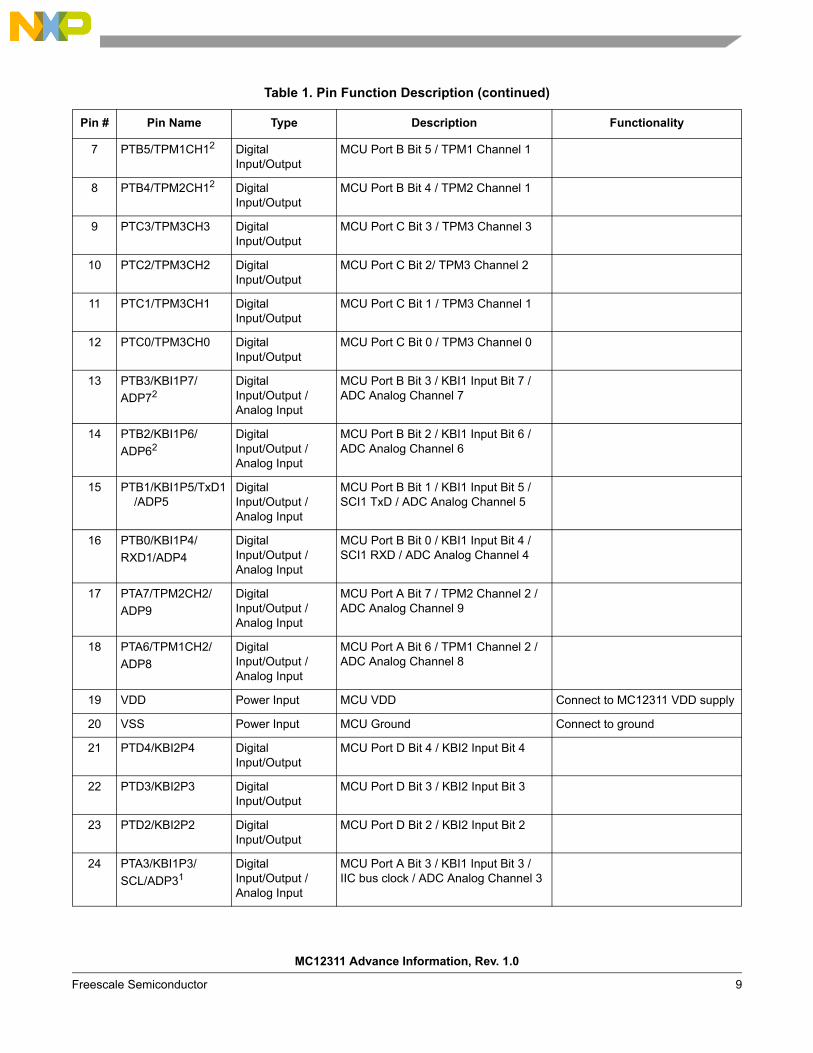
5.1 Pin DefinitionsTable 1 details the MC12311 pinout and functionality.
Table 1. Pin Function Description
Pin # Pin Name Type Description Functionality
1 VREFH Input MCU high reference voltage for ATD
2 VREFL Input MCU low reference voltage for ATD
3 VSSAD Power Input MCU ADC Ground Connect to ground
4 VSS Power Input MCU Ground Connect to ground
5 EXTAL/SCL/PTB71 Input / Digital Input/Output
MCU Crystal Oscillator input / IIC bus clock / Port B Bit 7
• Normally used as MCU clock source
• Driven from transceiver ClkOut (DIO5)
6 XTAL/SDA/PTB61 Output / Digital Input/Output
MCU Crystal Oscillator output / IIC bus data / Port B Bit 6
VDD
AD
VDD
1
DIO
5/C
LKO
UT
XTA
DIO
4
DIO
3
DIO
2
DIO
1/PT
D0/
KB
I2P0
DIO
0/PT
D1/
KB
I2P1
RES
ET
XTB
VR_D
IG
VR_A
NA
PA_BOOST
GND_PA1 (RF)
RFIO (RF)
GND_PA2 (RF)
RXTX (RF)
GND
VBAT2
PTA4/BKGD/MS
PTA5/IRQ/RESETB
PTC4
PTC5
NC
PTC6
PTB
1
PTB
0
PTA
7
PTA
6
VDD
VSS
PTD
4
PTD
3
PTD
2
PTA
3
PTA
2
PTA
1
1VREFH
VREFL
VSSAD
VSS
EXTAL/PTB7
XTAL/PTB6
PTB5
PTB4
PTC3
PTC2
PTC1
PTC0
PTB3
2
3
4
5
6
7
8
9
10
11
12
13
39
38
37
36
35
34
33
32
31
30
29
2615 16 17 18 19 20 21 22 23 24 25
53 52 51 50 49 48 47 46 45 44 4355 54
PTB2 14
PTA
0
PTC
72827
VR_PA (RF)
40
41
42
56
VBA
T1 (R
F)
57 58
6059
MC12311 FlagOpening
FlagOpening
Pads 57-60 Located on Bottom -
Pad 57 – SPSCKPad 58 – MOSIPad 59 – NSSPad 60 – MISO
MC12311 Advance Information, Rev. 1.0
Freescale Semiconductor 9
7 PTB5/TPM1CH12 Digital Input/Output
MCU Port B Bit 5 / TPM1 Channel 1
8 PTB4/TPM2CH12 Digital Input/Output
MCU Port B Bit 4 / TPM2 Channel 1
9 PTC3/TPM3CH3 Digital Input/Output
MCU Port C Bit 3 / TPM3 Channel 3
10 PTC2/TPM3CH2 Digital Input/Output
MCU Port C Bit 2/ TPM3 Channel 2
11 PTC1/TPM3CH1 Digital Input/Output
MCU Port C Bit 1 / TPM3 Channel 1
12 PTC0/TPM3CH0 Digital Input/Output
MCU Port C Bit 0 / TPM3 Channel 0
13 PTB3/KBI1P7/ADP72
Digital Input/Output / Analog Input
MCU Port B Bit 3 / KBI1 Input Bit 7 /ADC Analog Channel 7
14 PTB2/KBI1P6/ADP62
Digital Input/Output / Analog Input
MCU Port B Bit 2 / KBI1 Input Bit 6 /ADC Analog Channel 6
15 PTB1/KBI1P5/TxD1/ADP5
Digital Input/Output / Analog Input
MCU Port B Bit 1 / KBI1 Input Bit 5 /SCI1 TxD / ADC Analog Channel 5
16 PTB0/KBI1P4/RXD1/ADP4
Digital Input/Output / Analog Input
MCU Port B Bit 0 / KBI1 Input Bit 4 /SCI1 RXD / ADC Analog Channel 4
17 PTA7/TPM2CH2/ADP9
Digital Input/Output / Analog Input
MCU Port A Bit 7 / TPM2 Channel 2 /ADC Analog Channel 9
18 PTA6/TPM1CH2/ADP8
Digital Input/Output / Analog Input
MCU Port A Bit 6 / TPM1 Channel 2 /ADC Analog Channel 8
19 VDD Power Input MCU VDD Connect to MC12311 VDD supply
20 VSS Power Input MCU Ground Connect to ground
21 PTD4/KBI2P4 Digital Input/Output
MCU Port D Bit 4 / KBI2 Input Bit 4
22 PTD3/KBI2P3 Digital Input/Output
MCU Port D Bit 3 / KBI2 Input Bit 3
23 PTD2/KBI2P2 Digital Input/Output
MCU Port D Bit 2 / KBI2 Input Bit 2
24 PTA3/KBI1P3/SCL/ADP31
Digital Input/Output / Analog Input
MCU Port A Bit 3 / KBI1 Input Bit 3 /IIC bus clock / ADC Analog Channel 3
Table 1. Pin Function Description (continued)
Pin # Pin Name Type Description Functionality

MC12311 Advance Information, Rev. 1.0
10 Freescale Semiconductor
25 PTA2/KBI1P2/SDA/ADP22
Digital Input/Output / Analog Input
MCU Port A Bit 2 / KBI1 Input Bit 2 /IIC bus data / ADC Analog Channel 2
26 PTA1/KBI1P1/TPM2CH0/ADP1/ACMP1-3
Digital Input/Output / Analog Input
MCU Port A Bit 1 / KBI1 Input Bit 1 /TPM2 Channel 0 /ADC Analog Channel 1 /ACMP1 Analog Input Minus
27 PTA0/KBI1P0/TPM1CH0/ADP0/ACMP1+3
Digital Input/Output / Analog Input
MCU Port A Bit 0 / KBI1 Input Bit 0 /TPM1 Channel 0 /ADC Analog Channel 0 /ACMP1 Analog Input Plus
28 PTC7/TXD2/ACMP2-
Digital Input/Output / Analog Input
MCU Port C Bit 7 / SCI2 TXD /ACMP2 Analog Input Minus
29 PTC6/RXD2/ACMP2+
Digital Input/Output
MCU Port C Bit 6 / SCI2 RXD /ACMP2 Analog Input Plus
30 NC No Connect
31 PTC5/TPM3CH5/ACMP2O
Digital Input/Output
MCU Port C Bit 5 / TPM3 Channel 5 /ACMP2 Output
32 PTC4/TPM3CH4 Digital Input/Output
MCU Port C Bit 5 / TPM3 Channel 5 /ACMP2 Output
33 PTA5/IRQ/TPM1CLK/RESETB
Digital Input/Output
MCU Port A Bit 5 / MCU IRQ /TPM1 Clock / MCU RESET
34 PTA4/ACMP1O/BKGD/MS
Digital Input/Output
MCU Port A Bit 4 / ACMP1 Output /Background Debug Port / Mode Select
35 VBAT2 Power Input Transceiver VDD Connect to MC12311 VDD supply
36 GND Power Input Transceiver Ground Connect to ground
37 RXTX (RF) Digital Output Transceiver Rx/Tx RF Switch Control Output; high when in TX
38 GND_PA2 (RF) Power Input Transceiver RF Ground Connect to ground
39 RFIO (RF) RF Input/Output Transceiver RF Input/Output
40 GND_PA1 (RF) Power Input Transceiver RF Ground Connect to ground
41 PA_BOOST RF Output Transceiver Optional High-Power PA Output
42 VR_PA Power Output Transceiver regulated output voltage for VR_PA use.
43 VBAT1 (RF) Power Input Transceiver VDD for RF circuitry Connect to MC12311 VDD supply
44 VR_ANA Power Output Transceiver regulated output voltage for analog circuitry.
Decouple to ground with 100 nF capacitor
Table 1. Pin Function Description (continued)
Pin # Pin Name Type Description Functionality

MC12311 Advance Information, Rev. 1.0
Freescale Semiconductor 11
45 VR_DIG Power Output Transceiver regulated output voltage for digital circuitry.
Decouple to ground with 100 nF capacitor
46 XTA Xtal Osc Transceiver crystal reference oscillator Connect to 32 MHz crystal and load capacitor
47 XTB Xtal Osc Transceiver crystal reference oscillator Connect to 32 MHz crystal and load capacitor
48 RESET Digital Input Transceiver hardware reset input Typically driven from MCU GPIO
49 DIO0/PTD1/KBI2P1 Digital Input/Output
Transceiver GPIO Bit 0 /MCU Port D Bit 1 / MCU KBI2 Bit 1
MCU IO and Transceiver IO connected onboard MC12311
50 DIO1/PTD0/KBI2P0 Digital Input/Output
Transceiver GPIO Bit 1 /MCU Port D Bit 0 / MCU KBI2 Bit 0
MCU IO and Transceiver IO connected onboard MC12311
51 DIO2 Digital Input/Output
Transceiver GPIO Bit 2
52 DIO3 Digital Input/Output
Transceiver GPIO Bit 3
53 DIO4 Digital Input/Output
Transceiver GPIO Bit 4
54 DIO5/CLKOUT Digital Input/Output
Transceiver GPIO Bit 5 / ClkOut Commonly programmed as ClkOut to supply MCU clock; connect to Pin 5
55 VDD1 Power Input MCU VDD supply Connect to MC12311 VDD supply
56 VDDAD Power Input MCU ADC VDD Connect to MC12311 VDD supply
57 SPSCK2 Digital Input/Output
SPI Port Clock driven from MCU Port E Bit 0
• MCU IO and Transceiver IO connected onboard MC12311
• MCU IO must be configured for this connection
58 MOSI2 Digital Input/Output
SPI Port MOSI signal connected to MCU Port E Bit 1
• MCU IO and Transceiver IO connected onboard MC12311
• MCU IO must be configured for this connection
59 NSS2 Digital Input/Output
SPI Port SS signal connected to MCU Port E Bit 3
• MCU IO and Transceiver IO connected onboard MC12311
• MCU IO must be configured for this connection
60 MISO2 Digital Input/Output
SPI Port MISO signal connected to MCU Port E Bit 2
• MCU IO and Transceiver IO connected onboard MC12311
• MCU IO must be configured for this connection
FLAG VSS Power input External package flag. Common VSS Connect to ground.1 IIC pins, SCL and SDA can be repositioned using the IICPS bit in SOPT2; default locations are PTA3 and PTA2.2 The SPI Port pin selection must be configured by software by writing the SPIPS Bit in Register SOPT23 If ADC and ACMP1 are both enabled, both modules have access to the pin.
Table 1. Pin Function Description (continued)
Pin # Pin Name Type Description Functionality

MC12311 Advance Information, Rev. 1.0
12 Freescale Semiconductor
5.2 Internal Functional InterconnectsThe MCU provides control to the transceiver through the SPI Port and receives status from the transceiver from the DIOx pins. Certain interconnects between the devices are routed onboard the SiP. In addition, the signals are brought out to external pads.
NOTE• As shown in Table 2, the MCU SPI Port pin selection must be
configured by software by writing the SPIPS bit in Register SOPT2• The transceiver DIO pins must be programmed to provide desired status
5.3 External Functional InterconnectsIn addition to the onboard device interconnection, other external connections between the MCU and the transceiver are common:
1. Freescale recommends programming the transceiver DIO5 signal as ClkOut - for lowest system cost, a single crystal configuration can be used where ClkOut can be used to supply the MCU clock by connection to EXTAL Pin 5. With a 32 MHz transceiver reference oscillator crystal, ClkOut can be programmed for frequencies of 32 MHz, 16 MHz, 8 MHz, 4 MHz, 2 MHz, and 1 MHz.
2. Freesacle recommends driving/controlling the transceiver reset from an MCU GPIO - This allows over-riding control of the transceiver from the system application.
3. The other DIO2-DIO4 status and RXTX signals can prove useful for monitoring the transceiver operation - the DIO4-DIO2 signals must be programmed to provide operational status. All signals must be connected externally to appropriate MCU GPIO for this function.
6 System and Power ManagementThe MC12311 consists of an independent transceiver and MCU. The MCU controls the transceiver through programming of the SPI Port, and sets its operational mode through this control channel. Total current draw for the MC12311 is dependent on the operation mode of both devices.
Table 2. MC12311 Internal Functional Interconnects
Pin # MCU Signal Transceiver Signal Description
49 PTD1/KBI2P1 DIO0 Transceiver DIO0 can be programmed to provide status to the MCU
50 PTD0/KBI2P0 DIO1 Transceiver DIO1 can be programmed to provide status to the MCU
57 PTE0/SPSCK SCK MCU SPI connection must be initiated, not default
58 PTE1/MOSI MOSI MCU SPI connection must be initiated, not default
59 PTE3/SS NSS MCU SPI connection must be initiated, not default
60 PTE2/MISO MISO MCU SPI connection must be initiated, not default

MC12311 Advance Information, Rev. 1.0
Freescale Semiconductor 13
6.1 Modes of OperationThe MCU is the host controller and has the following primary modes of operation:
• Stop2 - provides lowest standby power consumption and maintains the contents of RAM and the current state of all of the I/O pins, but the main oscillator and most other digital circuitry are off. Wake-up is treated as a system recovery from reset.
• Stop3 - provides very low standby power consumption and maintains the contents of RAM, registers, and the current state of all of the I/O pins, but the main oscillator can be enabled or not. Wake-up is treated as an interrupt request, and this provides faster recovery time
• Wait - entered by executing a WAIT command, the CPU enters a low power state. This state can be used to save power over a normal RUN condition, but is not a true low power state such as Stop2 or Stop3
• Run - normal run condition for the CPU. Current draw is very dependent on the CPU clock frequency. Additional current can be saved but running at a lower clock rate if the software performance.
The transceiver has the following modes of operation:• Sleep - provides lowest power consumption and is the full power down state• Idle - provides very low standby power consumption and has the main voltage regulator and the
RC oscillator enabled• Standby - similar to Idle with low standby power consumption but has the main voltage regulator
and the crystal oscillator enabled• FS (Frequency synthesizer) - the frequency synthesizer is alive to shorten startup time to transmit
or receive states• Transmit - transmitter is active• Receive - receiver is active
6.2 Power ManagementThe MC12311 power management is controlled through programming of the modes of operation. Different modes allow for different levels of power-down. Additional features include:
• Transceiver Sleep with MCU Stop2 is the lowest power state• The transceiver mode is independent of the MCU• The transceiver uses/powers-up the transmitter or receiver only as required• MCU peripheral control clock gating can be disabled on a module-by-module basis to provide
lowest power• RTC can be used as wake-up timer• Wake-up available through KBI asynchronous interrupts and UART activity• Wake-up available with RTC

MC12311 Advance Information, Rev. 1.0
14 Freescale Semiconductor
6.3 System ProtectionThe MC12311 provides several vehicles to maintain security or a high level of system robustness:
• Watchdog computer operating properly (COP) reset with option to run from dedicated 1 kHz internal clock source or bus clock
• Low-voltage detection with reset or interrupt; selectable trip points• Illegal opcode detection with reset• Illegal address detection with reset• Flash block protection
7 Development EnvironmentDevelopment support for the HCS08 on the MC12311 includes the background debug controller (BDC) and the on-chip debug module (DBG). The BDC provides a single-wire debug interface to the MCU that provides a convenient interface for programming the on-chip FLASH and other storage. The BDC is also the primary debug interface for development and allows non-intrusive access to memory data and traditional debug features such as CPU register modify, breakpoints, and single instruction trace commands.
Address and data bus signals are not available on external pins. Debug is done through commands fed into the MCU via the single-wire background debug interface. The debug module provides a means to selectively trigger and capture bus information so an external development system can reconstruct what happened inside the MCU on a cycle-by-cycle basis without having external access to the address and data signals. Features include:
• Single-wire background debug interface• Breakpoint capability to allow single breakpoint setting during in-circuit debugging (plus two
more breakpoints)• On-chip in-circuit emulator (ICE) debug module containing two comparators and nine trigger
modes
8 System Electrical SpecificationThis section details maximum ratings for the 60 pin LGA package and recommended operating conditions, DC characteristics, and AC characteristics for the modem, and the MCU.
8.1 SiP LGA Package Maximum RatingsAbsolute maximum ratings are stress ratings only, and functional operation at the maximum rating is not guaranteed. Stress beyond the limits specified in Table 3 may affect device reliability or cause permanent damage to the device. For functional operating conditions, refer to the remaining tables in this section.
This device contains circuitry protecting against damage due to high static voltage or electrical fields; however, it is advised that normal precautions be taken to avoid application of any voltages higher than maximum-rated voltages to this high-impedance circuit. Reliability of operation is enhanced if unused

MC12311 Advance Information, Rev. 1.0
Freescale Semiconductor 15
inputs are tied to an appropriate logic voltage level (for instance, either VSS or VDD) or the programmable pull-up resistor associated with the pin is enabled.
Table 3 shows the maximum ratings for the 60 Pin LGA package.
8.2 ESD Protection and Latch-Up ImmunityAlthough damage from electrostatic discharge (ESD) is much less common on these devices than on early CMOS circuits, normal handling precautions should be used to avoid exposure to static discharge. Qualification tests are performed to ensure that these devices can withstand exposure to reasonable levels of static without suffering any permanent damage.
All ESD testing is in conformity with the JESD22 Stress Test Qualification for Commercial Grade Integrated Circuits. During the device qualification ESD stresses were performed for the human body model (HBM), the machine model (MM) and the charge device model (CDM).
All latchup testing is in conformity with the JESD78 IC Latch-Up Test.
A device is defined as a failure if after exposure to ESD pulses the device no longer meets the device specification.
Table 3. LGA Package Maximum Ratings
Rating Symbol Value Unit
Maximum Junction Temperature TJ 95 °C
Storage Temperature Range Tstg -55 to 115 °C
Power Supply Voltage VBATT, VDDINT -0.3 to 3.8 Vdc
Digital Input Voltage Vin -0.3 to (VDDINT + 0.3)
RF Input Power Pmax 6 dBm
Note: Maximum Ratings are those values beyond which damage to the device may occur. Functional operation should be restricted to the limits in the Electrical Characteristics or Recommended Operating Conditions tables.
Note: Meets Human Body Model (HBM) = 2 kV. RF input/output pins have no ESD protection.
Table 4. ESD and Latch-up Test Conditions
Model Description Symbol Value Unit
Human Body
Series resistance R1 1500 Ω
Storage capacitance C 100 pF
Number of pulses per pin1
1 This number represents a minimum number for both positive pulse(s) and negative pulse(s)
— 1
Machine
Series resistance R1 0 Ω
Storage capacitance C 200 pF
Number of pulses per pin1 — 1
Latch-upMinimum input voltage limit – 1.8 V
Maximum input voltage limit 4.32 V

MC12311 Advance Information, Rev. 1.0
16 Freescale Semiconductor
8.3 Transceiver Electrical CharacteristicsThe tables below give the electrical specifications of the transceiver under the following conditions: Supply voltage VBAT1= VBAT2=VDD=3.3 V, temperature = 25 °C, FXOSC = 32 MHz, FRF = 915 MHz, Pout = +13dBm, 2-level FSK modulation without pre-filtering, FDA = 5 kHz, Bit Rate = 4.8 kb/s and terminated in a matched 50 Ohm impedance, unless otherwise specified.
NOTEUnless otherwise specified, the performances in the other frequency bands are similar or better.
8.3.1 Transceiver Recommended Operating Conditions
Table 5. ESD and Latch-Up Protection Characteristics
No. Rating1
1 Parameter is achieved by design characterization on a small sample size from typical devices under typical conditions unless otherwise noted.
Symbol Min Max Unit
1 Human body model (HBM) VHBM ± 2000 — V
2 Machine model (MM) VMM ± 200 — V
3 Charge device model (CDM) VCDM ± 750 — V
4 Latch-up current at TA = 85°C ILAT ± 100 — mA
Table 6. Recommended Operating Conditions
Characteristic Symbol Min Typ Max Unit
Power Supply Voltage (VBATT) 1.8 3.6 Vdc
Operating Temperature Range TA -40 25 85 °C
Logic Input Voltage Low VIL 0 - 20% VBATT
V
Logic Input Voltage High VIH 80% VBATT
- VBATT V
Logic Output Voltage Low (Imax = -1 mA) VOL 0 - 10% VBATT
V
Logic Output Voltage High (Imax = 1 mA) VOH 90% VBATT
- VBATT V
Load capacitance on digital ports CL 25 pF
SPI Clock Rate fSPI - - 8.0 MHz
RF Input Power Pmax - - 0 dBm
Crystal Reference Oscillator Frequency fref 32 MHz Only

MC12311 Advance Information, Rev. 1.0
Freescale Semiconductor 17
8.3.2 Transceiver Power Consumption
8.3.3 Transceiver Frequency Synthesis
Table 7. Power Supply Current
Characteristic Conditions Symbol Min Typ Max Unit
Supply current in Sleep mode IDDSL - 0.1 1 µA
Supply current in Idle mode RC oscillator enabled IDDIDLE - 1.2 - µA
Supply current in Standby mode Crystal oscillator enabled IDDST - 1.25 1.5 mA
Supply current in Synthesizer mode IDDFS - 9 - mA
Supply current in Receive mode IDDR - 16 - mA
Supply current in Transmit mode with appropriate matching, stable across VDD range
RFOP = +17 dBm, on PA_BOOSTRFOP = +13 dBm, on RFIO pinRFOP = +10 dBm, on RFIO pinRFOP = 0 dBm, on RFIO pinRFOP = -1 dBm, on RFIO pin
IDDT -----
9545332016
-----
mAmAmAmAmA
Table 8. Frequency Synthesizer Specification
Characteristic Conditions Symbol Min Typ Max Unit
Synthesizer Frequency Range Programmable FR 290424862
---
340510
1020
MHzMHzMHz
Crystal oscillator frequency FXOSC - 32 - MHz
Crystal oscillator wake-up time TS_OSC - 250 500 µs
Frequency synthesizer wake-up time to PllLock signal
From Standby mode TS_FS - 80 150 µs
Frequency synthesizer hop time at most 10 kHz away from the target
200 kHz step1 MHz step5 MHz step7 MHz step
12 MHz step20 MHz step25 MHz step
TS_HOP -------
20205050808080
-------
µsµsµsµsµsµsµs
Frequency synthesizer step FSTEP = FXOSC/219 FSTEP - 61.0 - Hz
RC Oscillator frequency After calibration FRC - 62.5 - kHz
Bit rate, FSK Programmable BRF 1.2 - 300 kbps
Bit rate, OOK Programmable BRO 1.2 - 32.768 kbps
Frequency deviation, FSK ProgrammableFDA + BRF/2 =< 500 kHz
FDA 0.6 - 300 kHz

MC12311 Advance Information, Rev. 1.0
18 Freescale Semiconductor
8.3.4 ReceiverAll receiver tests are performed with RxBw = 10 kHz (Single Side Bandwidth) as programmed in RegRxBw, receiving a PN15 sequence with a BER of 0.1% (Bit Synchronizer is enabled), unless otherwise specified. The LNA impedance is set to 200 Ohms, by setting bit LnaZin in RegLna to 1. Blocking tests are performed with an unmodulated interferer. The wanted signal power for the Blocking Immunity, ACR, IIP2, IIP3 and AMR tests is set 3 dB above the nominal sensitivity level.
Table 9. Receiver Specification
Characteristic Conditions Symbol Min Typ Max Unit
FSK sensitivity, highest LNA gain FDA = 5 kHz, BR = 1.2 kb/sFDA = 5 kHz, BR = 4.8 kb/sFDA = 40 kHz, BR = 38.4 kb/s
RFS_F ---
-118-114-105
---
dBmdBmdBm
FDA = 5 kHz, BR = 1.2 kb/s 1 - -120 - dBm
OOK sensitivity, highest LNA gain BR = 4.8 kb/s RFS_O - -112 -109 dBm
Co-Channel Rejection CCR -13 -10 - dB
Adjacent Channel Rejection Offset = +/- 25 kHzOffset = +/- 50 kHz
ACR -37
4242
--
dBdB
Blocking Immunity Offset = +/- 1 MHzOffset = +/- 2 MHz
Offset = +/- 10 MHz
BI ---
-45-40-32
---
dBmdBmdBm
Blocking ImmunityWanted signal at sensitivity +16dB
Offset = +/- 1 MHzOffset = +/- 2 MHz
Offset = +/- 10 MHz
---
-36-33-25
---
dBmdBmdBm
AM Rejection , AM modulated interferer with 100% modulation depth, fm = 1 kHz, square
Offset = +/- 1 MHzOffset = +/- 2 MHz
Offset = +/- 10 MHz
AMR ---
-45-40-32
---
dBmdBmdBm
2nd order Input Intercept PointUnwanted tones are 20 MHz above the LO
Lowest LNA gainHighest LNA gain
IIP2 --
+75+35
--
dBmdBm
3rd order Input Intercept pointUnwanted tones are 1MHz and 1.995 MHz above the LO
Lowest LNA gainHighest LNA gain
IIP3 --23
+20-18
--
dBmdBm
Single Side channel filter BW Programmable BW_SSB 2.6 - 500 kHz
Image rejection in OOK mode Wanted signal level = -106 dBm IMR_OOK
27 30 - dB
Receiver wake-up time, from PLL locked state to RxReady
RxBw = 10 kHz, BR = 4.8 kb/sRxBw = 200 kHz, BR = 100 kb/s
TS_RE --
1.796
--
msµs
Receiver wake-up time, from PLL locked state, AGC enabled
RxBw= 10 kHz, BR = 4.8 kb/sRxBw = 200 kHz, BR = 100 kb/s
TS_RE_AGC
- 3.0163
msµs
Receiver wake-up time, from PLL lock state, AGC and AFC enabled
RxBw= 10 kHz, BR = 4.8 kb/sRxBw = 200 kHz, BR = 100 kb/s
TS_RE_AGC&AFC
4.8265
msµs
FEI sampling time Receiver is ready TS_FEI - 4.Tbit - -
AFC Response Time Receiver is ready TS_AFC - 4.Tbit - -

MC12311 Advance Information, Rev. 1.0
Freescale Semiconductor 19
8.3.5 Transmitter
8.4 MCU Electrical CharacteristicsThe following sections describe the electrical characteristics of the MC12311 MCU.
8.4.1 MCU DC CharacteristicsThis section includes information about power supply requirements and I/O pin characteristics.
RSSI Response Time Receiver is ready TS_RSSI - 2.Tbit - -
RSSI Dynamic Range AGC enabled Min Max
DR_RSSI --
-1150
--
dBmdBm
1 Set SensitivityBoost in RegTestLna to 0x2D to reduce the noise floor in the receiver
Table 10. Transmitter Specidication
Characteristic Conditions Symbol Min Typ Max Unit
RF output power in 50 ohmsOn RFIO pin
Programmable with 1dB steps MaxMin
RF_OP --
+13-18
--
dBmdBm
Max RF output power, on PA_BOOST pin
With external match to 50 ohms RF_OPH - +17 - dBm
RF output power stability From VDD=1.8V to 3.6V ΔRF_OP - +/-0.3 - dB
Transmitter Phase Noise 50 kHz Offset from carrier 868 / 915 MHz bands 434 / 315 MHz bands
PHN --
-95-99
--
dBc/Hz
Transmitter adjacent channel power (measured at 25 kHz offset)
BT=0.5 . Measurement conditions as defined by EN 300 220-1 V2.1.1
ACP - - -37 dBm
Transmitter wake up time, to the first rising edge of DCLK
Frequency Synthesizer enabled, PaRamp = 10 µs, BR = 4.8 kb/s.
TS_TR - 120 - µs
Table 11. DC Characteristics
Num C Characteristic Symbol Condition Min Typ1 Max Unit
1 Operating Voltage 1.82 3.6 V
2
C Output high voltage
All I/O pins,low-drive strength
VOH
1.8 V, ILoad = –2 mA VDD – 0.5 — —
VP All I/O pins,high-drive strength
2.7 V, ILoad = –10 mA VDD – 0.5 — —
T 2.3 V, ILoad = –6 mA VDD – 0.5 — —
C 1.8V, ILoad = –3 mA VDD – 0.5 — —
Table 9. Receiver Specification
Characteristic Conditions Symbol Min Typ Max Unit

MC12311 Advance Information, Rev. 1.0
20 Freescale Semiconductor
3 D Output high current
Max total IOH for allports IOHT — — 100 mA
4
C Output low voltage
All I/O pins,low-drive strength
VOL
1.8 V, ILoad = 2 mA — — 0.5
VP All I/O pins,high-drive strength
2.7 V, ILoad = 10 mA — — 0.5
T 2.3 V, ILoad = 6 mA — — 0.5
C 1.8 V, ILoad = 3 mA — — 0.5
D Output low current
Max total IOL for allports IOLT — — 100 mA5
6P Input high
voltageall digital inputs
VIHVDD > 2.7 V 0.70 x VDD — —
VC VDD > 1.8 V 0.85 x VDD — —
7P Input low voltage all digital inputs
VILVDD > 2.7 V — — 0.35 x VDD
C VDD >1.8 V — — 0.30 x VDD
8 C Input hysteresis all digital inputs Vhys 0.06 x VDD — — mV
9 P Input leakage current
all input only pins(Per pin) |IIn| VIn = VDD or VSS — — 1 μA
10 P Hi-Z (off-state) leakage current
all input/output(per pin) |IOZ| VIn = VDD or VSS — — 1 μA
11 P
Total leakage combined for all inputs and Hi-Z pins
All input only and I/O
|IOZTOT| VIn = VDD or VSS — — 2 μA
12 PPull-up resistors all digital inputs, when
enabled RPU 17.5 — 52.5 kΩ
13 DDC injection current 3, 4, 5
Single pin limitIIC VIN < VSS, VIN > VDD
–0.2 — 0.2 mA
Total MCU limit, includessum of all stressed pins –5 — 5 mA
14 C Input Capacitance, all pins CIn — — 8 pF
15 C RAM retention voltage VRAM — 0.6 1.0 V
16 C POR re-arm voltage6 VPOR 0.9 1.4 1.79 V
Table 11. DC Characteristics (continued)
Num C Characteristic Symbol Condition Min Typ1 Max Unit

NOTES
MC12311 Advance Information, Rev. 1.0
Freescale Semiconductor 21
Figure 6. Pull-up and Pull-down Typical Resistor Values
17 D POR re-arm time tPOR 10 — — μs
P Low-voltage detection threshold —high range7 VLVDH
8 VDD fallingVDD rising
2.112.16
2.162.21
2.222.27 V18
P Low-voltage detection threshold —low range7 VLVDL
VDD fallingVDD rising
1.801.86
1.821.90
1.911.99 V19
P Low-voltage warning threshold —high range7 VLVWH
VDD fallingVDD rising
2.362.36
2.462.46
2.562.56 V20
P Low-voltage warning threshold —low range7 VLVWL
VDD fallingVDD rising
2.112.16
2.162.21
2.222.27 V21
C Low-voltage inhibit reset/recover hysteresis7 Vhys — 50 — mV22
23 P Bandgap Voltage Reference9 VBG 1.15 1.17 1.18 V1 Typical values are measured at 25°C. Characterized, not tested2 As the supply voltage rises, the LVD circuit will hold the MCU in reset until the supply has risen above VLVDL.3 All functional non-supply pins are internally clamped to VSS and VDD.4 Input must be current limited to the value specified. To determine the value of the required current-limiting resistor, calculate
resistance values for positive and negative clamp voltages, then use the larger of the two values.5 Power supply must maintain regulation within operating VDD range during instantaneous and operating maximum current
conditions. If positive injection current (VIn > VDD) is greater than IDD, the injection current may flow out of VDD and could result in external power supply going out of regulation. Ensure external VDD load will shunt current greater than maximum injection current. This will be the greatest risk when the MCU is not consuming power. Examples are: if no system clock is present, or if clock rate is very low (which would reduce overall power consumption).
6 Maximum is highest voltage that POR is guaranteed.7 Low voltage detection and warning limits measured at 1 MHz bus frequency.8 Run at 1 MHz bus frequency9 Factory trimmed at VDD = 3.0 V, Temp = 25°C
Table 11. DC Characteristics (continued)
Num C Characteristic Symbol Condition Min Typ1 Max Unit
PULL-UP RESISTOR TYPICALS
VDD (V)
PULL
-UP
RES
ISTO
R (k
Ω)
20
25
30
35
40
1.8 2 2.2 2.4 2.6 2.8 3 3.2 3.4 3.6
25°C85°C
–40°C
PULL-DOWN RESISTOR TYPICALS
VDD (V)
PULL
-DO
WN
RES
ISTA
NC
E (k
Ω)
20
25
30
35
40
1.8 2.3 2.8 3.3
25°C85°C
–40°C
3.6

MC12311 Advance Information, Rev. 1.0
22 Freescale Semiconductor
Figure 7. Typical Low-Side Driver (Sink) Characteristics — Low Drive (PTxDSn = 0)
Figure 8. Typical Low-Side Driver (Sink) Characteristics — High Drive (PTxDSn = 1)
Figure 9. Typical High-Side (Source) Characteristics — Low Drive (PTxDSn = 0)
TYPICAL VOL VS IOL AT VDD = 3.0 V
IOL (mA)
V OL
(V)
0
0.2
0.4
0.6
0.8
1
1.2
0 5 10 15 20
TYPICAL VOL VS VDD
VDD (V)
V OL
(V)
0
0.05
0.1
0.15
0.2
1 2 3 4
25°C85°C
–40°C
25°C, IOL = 2 mA85°C, IOL = 2 mA
–40°C, IOL = 2 mA
TYPICAL VOL VS IOL AT VDD = 3.0 V
IOL (mA)
V OL
(V)
0
0.2
0.4
0.6
0.8
1
0 10 20 30
TYPICAL VOL VS VDD
VDD (V)
V OL
(V)
0
0.1
0.2
0.3
0.4
1 2 3 4
IOL = 6 mA
IOL = 3 mA
IOL = 10 mA
25°C85°C
–40°C 25°C85°C
–40°C
TYPICAL VDD – VOH VS IOH AT VDD = 3.0 V
IOH (mA))
0
0.2
0.4
0.6
0.8
1
1.2
–20–15–10–50
TYPICAL VDD – VOH VS VDD AT SPEC IOH
VDD (V)
V DD
– V
OH
(V)
0
0.05
0.1
0.15
0.2
0.25
1 2 3 4
V DD
– V
OH
(V) 25°C
85°C
–40°C 25°C, IOH = 2 mA85°C, IOH = 2 mA
–40°C, IOH = 2 mA

MC12311 Advance Information, Rev. 1.0
Freescale Semiconductor 23
Figure 10. Typical High-Side (Source) Characteristics — High Drive (PTxDSn = 1)
8.4.2 MCU Supply Current CharacteristicsThis section includes information about power supply current in various operating modes.
Table 12. Supply Current Characteristics
Num C Parameter Symbol BusFreq
VDD (V) Typ1 Max Unit Temp
(°C)
1
P Run supply currentFEI mode, all modules on
RIDD
25.165 MHz
3
13 184
mA
–40 to 25
P 14 15 85
T 20 MHz 13.75 —
–40 to 85T 8 MHz 5.59 —
T 1 MHz 1.03 —
2
C Run supply currentFEI mode, all modules off
RIDD
25.165 MHz
3
11.5 12.3
mA –40 to 85T 20 MHz 9.5 —
T 8 MHz 4.6 —
T 1 MHz 1.0 —
3T Run supply current
LPS=0, all modules offRIDD
16 kHz FBILP
3152 —
μA –40 to 85T 16 kHz
FBELP 115 —
4
TRun supply currentLPS=1, all modules off, running from Flash
RIDD16 kHz FBELP 3
21.9—
μA
0 to 70
— –40 to 85
TRun supply currentLPS=1, all modules off, running from RAM
7.3— 0 to 70
— –40 to 85
5
C Wait mode supply currentFEI mode, all modules off
WIDD
25.165 MHz
3
5.74 6
mA –-40 to 85T 20 MHz 4.57 —
T 8 MHz 2 —
T 1 MHz 0.73 —
TYPICAL VDD – VOH VS IOH AT VDD = 3.0 V
IOH (mA)
0
0.2
0.4
0.6
0.8
–30–25–20–15–10–50
TYPICAL VDD – VOH VS VDD AT SPEC IOH
VDD (V)
V DD
– V
OH
(V)
0
0.1
0.2
0.3
0.4
1 2 3 4
IOH = –10 mA
IOH = –6 mA
IOH = –3 mAV DD
– V
OH
(V)
25°C85°C
–40°C
25°C85°C
–40°C

MC12311 Advance Information, Rev. 1.0
24 Freescale Semiconductor
6
P Stop2 mode supply current
S2IDD n/a
3
0.35 0.65
μA
-40 to 25
C 0.8 1.0 70
P 2.0 4.5 85
C
2
0.25 0.5 -40 to 25
C 0.65 0.85 70
C 1.5 3.5 85
7
P Stop3 mode supply currentNo clocks active
S3IDD n/a
3
0.45 1.0
μA
-40 to 25
C 1.5 2.3 70
P 4 8 85
C
2
0.35 0.7 -40 to 25
C 1 2 70
C 3.5 6.0 85
8 T
Low power mode adders:
EREFSTEN=1 32 kHz
3
500 nA
-40 to 85
9 T IREFSTEN=1 32 kHz 70 μA
10 T TPM PWM 100 Hz 12 nA
11 T SCI, SPI, or IIC 300 bps 15 μA
12 T RTC using LPO 1 kHz 200 μA
13 T RTC using ICSERCLK 32 kHz 1 μA
14 T LVD n/a 100 μA
15 T ACMP n/a 20 μA1 Data in Typical column was characterized at 3.0 V, 25°C or is typical recommended value.
Table 13. Stop Mode Adders
Num C Parameter ConditionTemperature (°C)
Units-40 25 70 85
1 T LPO 50 75 100 150 nA
2 T ERREFSTEN RANGE = HGO = 0 1000 1000 1100 1500 nA
3 T IREFSTEN1 63 70 77 81 uA
4 T RTC does not include clock source current 50 75 100 150 nA
5 T LVD1 LVDSE = 1 90 100 110 115 uA
6 T ACMP1 not using the bandgap (BGBE = 0) 18 20 22 23 uA
7 T ADC1 ADLPC = ADLSMP = 1 not using the bandgap (BGBE = 0)
95 106 114 120 uA
Table 12. Supply Current Characteristics (continued)
Num C Parameter Symbol BusFreq
VDD (V) Typ1 Max Unit Temp
(°C)

MC12311 Advance Information, Rev. 1.0
Freescale Semiconductor 25
8.4.3 External Oscillator (XOSCVLP) CharacteristicsReference Figure 11 and Figure 12 for crystal or resonator circuits.
1 Not available in stop2 mode.
Table 14. XOSC and ICS Specifications (Temperature Range = –40 to 85°C Ambient)
Num C Characteristic Symbol Min Typ1
1 Data in Typical column was characterized at 3.0 V, 25°C or is typical recommended value.
Max Unit
1 C
Oscillator crystal or resonator (EREFS = 1, ERCLKEN = 1)Low range (RANGE = 0)High range (RANGE = 1), high gain (HGO = 1)High range (RANGE = 1), low power (HGO = 0)
flofhifhi
3211
———
38.4168
kHzMHzMHz
2 DLoad capacitors
Low range (RANGE=0), low power (HGO=0)Other oscillator settings
C1,C2See Note2
See Note3
2 Load capacitors (C1,C2), feedback resistor (RF) and series resistor (RS) are incorporated internally when RANGE=HGO=0.3 See crystal or resonator manufacturer’s recommendation.
3 D
Feedback resistorLow range, low power (RANGE=0, HGO=0)2Low range, High Gain (RANGE=0, HGO=1)High range (RANGE=1, HGO=X)
RF———
—101
———
MΩ
4 D
Series resistor — Low range, low power (RANGE = 0, HGO = 0)2Low range, high gain (RANGE = 0, HGO = 1)High range, low power (RANGE = 1, HGO = 0)High range, high gain (RANGE = 1, HGO = 1)
≥ 8 MHz4 MHz1 MHz
RS
———
———
—0
100
000
———
01020
kΩ
5 C
Crystal start-up time 4Low range, low powerLow range, high powerHigh range, low powerHigh range, high power
4 Proper PC board layout procedures must be followed to achieve specifications.
tCSTL
tCSTH
————
200400
515
————
ms
6 DSquare wave input clock frequency (EREFS = 0, ERCLKEN = 1)
FEE or FBE mode FBELP mode
fextal 0.031250
——
40.050.33
MHzMHz
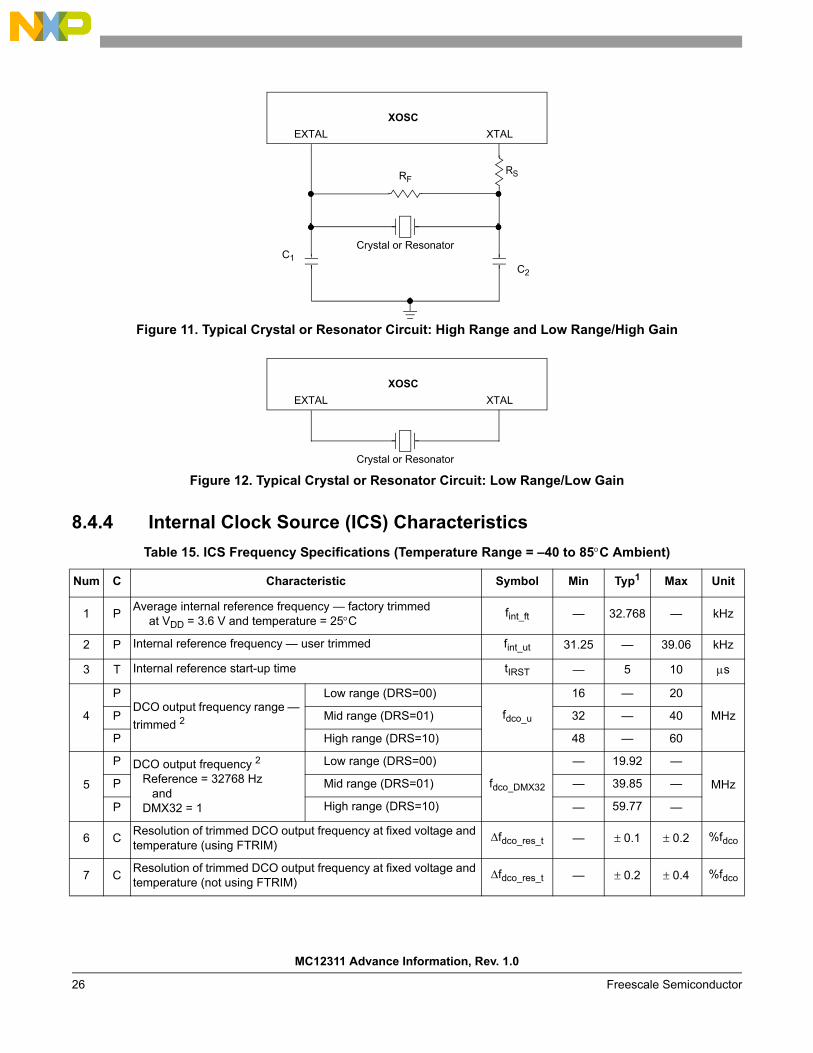
MC12311 Advance Information, Rev. 1.0
26 Freescale Semiconductor
Figure 11. Typical Crystal or Resonator Circuit: High Range and Low Range/High Gain
Figure 12. Typical Crystal or Resonator Circuit: Low Range/Low Gain
8.4.4 Internal Clock Source (ICS) CharacteristicsTable 15. ICS Frequency Specifications (Temperature Range = –40 to 85°C Ambient)
Num C Characteristic Symbol Min Typ1 Max Unit
1 P Average internal reference frequency — factory trimmed at VDD = 3.6 V and temperature = 25°C
fint_ft — 32.768 — kHz
2 P Internal reference frequency — user trimmed fint_ut 31.25 — 39.06 kHz
3 T Internal reference start-up time tIRST — 5 10 μs
4
PDCO output frequency range — trimmed 2
Low range (DRS=00)
fdco_u
16 — 20
MHzP Mid range (DRS=01) 32 — 40
P High range (DRS=10) 48 — 60
5
P DCO output frequency 2Reference = 32768 Hz
andDMX32 = 1
Low range (DRS=00)
fdco_DMX32
— 19.92 —
MHzP Mid range (DRS=01) — 39.85 —
P High range (DRS=10) — 59.77 —
6 C Resolution of trimmed DCO output frequency at fixed voltage and temperature (using FTRIM)
Δfdco_res_t — ± 0.1 ± 0.2 %fdco
7 C Resolution of trimmed DCO output frequency at fixed voltage and temperature (not using FTRIM)
Δfdco_res_t — ± 0.2 ± 0.4 %fdco
XOSCEXTAL XTAL
Crystal or Resonator
RS
C2
RF
C1
XOSCEXTAL XTAL
Crystal or Resonator

MC12311 Advance Information, Rev. 1.0
Freescale Semiconductor 27
8.4.5 MCU AC CharacteristicsThis section describes timing characteristics for each peripheral system.
8.4.5.1 Control Timing
8 C Total deviation of trimmed DCO output frequency over voltage and temperature
Δfdco_t — + 0.5-1.0 ± 2 %fdco
9 CTotal deviation of trimmed DCO output frequency over fixed voltage and temperature range of 0°C to 70 °C
Δfdco_t — ± 0.5 ± 1 %fdco
10 C FLL acquisition time 3 tAcquire — — 1 ms
11 CLong term jitter of DCO output clock (averaged over 2-ms interval) 4
CJitter — 0.02 0.2 %fdco
1 Data in Typical column was characterized at 3.0 V, 25°C or is typical recommended value.2 The resulting bus clock frequency should not exceed the maximum specified bus clock frequency of the device.3 This specification applies to any time the FLL reference source or reference divider is changed, trim value changed or changing
from FLL disabled (FBELP, FBILP) to FLL enabled (FEI, FEE, FBE, FBI). If a crystal/resonator is being used as the reference, this specification assumes it is already running.
4 Jitter is the average deviation from the programmed frequency measured over the specified interval at maximum fBus. Measurements are made with the device powered by filtered supplies and clocked by a stable external clock signal. Noise injected into the FLL circuitry via VDD and VSS and variation in crystal oscillator frequency increase the CJitter percentage for a given interval.
Table 16. Control Timing
Num C Rating Symbol Min Typ1 Max Unit
1 D
Bus frequency (tcyc = 1/fBus)VDD ≥ 1.8VVDD > 2.1VVDD > 2.4V
fBus dc ———
1020
25.165
MHz
2 D Internal low power oscillator period tLPO 700 — 1300 μs
3 D External reset pulse width2 textrst 100 — — ns
4 D Reset low drive trstdrv 34 x tcyc — — ns
5 D BKGD/MS setup time after issuing background debug force reset to enter user or BDM modes tMSSU 500 — — ns
6 D BKGD/MS hold time after issuing background debug force reset to enter user or BDM modes 3 tMSH 100 — — μs
7 DIRQ pulse width
Asynchronous path2
Synchronous path4tILIH, tIHIL 100
1.5 x tcyc
——
—— ns
Table 15. ICS Frequency Specifications (Temperature Range = –40 to 85°C Ambient) (continued)
Num C Characteristic Symbol Min Typ1 Max Unit

MC12311 Advance Information, Rev. 1.0
28 Freescale Semiconductor
Figure 13. Reset Timing
Figure 14. IRQ/KBIPx Timing
8.4.6 TPM Module TimingSynchronizer circuits determine the shortest input pulses that can be recognized or the fastest clock that can be used as the optional external source to the timer counter. These synchronizers operate from the current bus rate clock.
8 DKeyboard interrupt pulse width
Asynchronous path2
Synchronous path4tILIH, tIHIL 100
1.5 x tcyc
——
—— ns
9 C
Port rise and fall time — Low output drive (PTxDS = 0) (load = 50 pF)5 Slew rate control disabled (PTxSE = 0) Slew rate control enabled (PTxSE = 1)
tRise, tFall ——
831
——
ns
Port rise and fall time — High output drive (PTxDS = 1) (load = 50 pF)
Slew rate control disabled (PTxSE = 0) Slew rate control enabled (PTxSE = 1)
tRise, tFall ——
724
——
ns
10 Voltage regulator recovery time tVRR — 4 — μs1 Typical values are based on characterization data at VDD = 3.0V, 25°C unless otherwise stated.2 This is the shortest pulse that is guaranteed to be recognized as a reset or interrupt pin request. Shorter pulses are not
guaranteed to override reset requests from internal sources.3 To enter BDM mode following a POR, BKGD/MS should be held low during the power-up and for a hold time of tMSH after VDD
rises above VLVD.4 This is the minimum pulse width that is guaranteed to pass through the pin synchronization circuitry. Shorter pulses may or
may not be recognized. In stop mode, the synchronizer is bypassed so shorter pulses can be recognized in that case.5 Timing is shown with respect to 20% VDD and 80% VDD levels. Temperature range –40°C to 85°C.
Table 16. Control Timing (continued)
Num C Rating Symbol Min Typ1 Max Unit
textrst
RESET PIN
tIHIL
KBIPx
tILIH
IRQ/KBIPx

MC12311 Advance Information, Rev. 1.0
Freescale Semiconductor 29
Figure 15. Timer External Clock
Figure 16. Timer Input Capture Pulse
8.4.7 ADC Characteristics
Table 17. TPM Input Timing
No. C Function Symbol Min Max Unit
1 D External clock frequency fTCLK 0 fBus/4 Hz
2 D External clock period tTCLK 4 — tcyc
3 D External clock high time tclkh 1.5 — tcyc
4 D External clock low time tclkl 1.5 — tcyc
5 D Input capture pulse width tICPW 1.5 — tcyc
Table 18. 12-bit ADC Operating Conditions
C Characteristic Conditions Symb Min Typ1 Max Unit Comment
DSupply voltage Absolute VDDA 1.8 — 3.6 V
Delta to VDD (VDD-VDDA)2 ΔVDDA -100 0 +100 mV
D Ground voltage Delta to VSS (VSS-VSSA)2 ΔVSSA -100 0 +100 mV
D Ref Voltage High VREFH 1.8 VDDA VDDA V
D Ref Voltage Low VREFL VSSA VSSA VSSA V
D Input Voltage VADIN VREFL — VREFH V
C Input Capacitance
CADIN — 4.5 5.5 pF
C Input Resistance RADIN — 5 7 kΩ
tTCLK
tclkh
tclkl
TCLK
tICPW
TPMCHn
tICPW
TPMCHn

MC12311 Advance Information, Rev. 1.0
30 Freescale Semiconductor
Figure 17. ADC Input Impedance Equivalency Diagram
C
Analog Source Resistance
12 bit modefADCK > 4MHzfADCK < 4MHz
RAS——
——
25
kΩ
External to MCU
10 bit modefADCK > 4MHzfADCK < 4MHz
——
——
510
8 bit mode (all valid fADCK) — — 10
DADC Conversion Clock Freq.
High Speed (ADLPC=0) fADCK 0.4 — 8.0MHz
Low Power (ADLPC=1) 0.4 — 4.01 Typical values assume VDDA = 3.0V, Temp = 25°C, fADCK=1.0MHz unless otherwise stated. Typical values are for reference
only and are not tested in production.2 DC potential difference.
Table 18. 12-bit ADC Operating Conditions (continued)
C Characteristic Conditions Symb Min Typ1 Max Unit Comment
+–
+
–VAS
RAS
CAS
VADIN
ZASPad leakagedue toinput protection
ZADIN
SIMPLIFIED INPUT PIN EQUIVALENT
CIRCUIT
RADIN
ADC SARENGINE
SIMPLIFIED CHANNEL SELECT
CIRCUIT
INPUT PIN
RADIN
CADIN
INPUT PIN
RADIN
INPUT PIN
RADIN

MC12311 Advance Information, Rev. 1.0
Freescale Semiconductor 31
Table 19. 12-bit ADC Characteristics (VREFH = VDDASSA, VREFL = VSSA)
Characteristic Conditions C Symb Min Typ1 Max Unit Comment
Supply CurrentADLPC=1ADLSMP=1ADCO=1
T IDDA — 120 —
μA
Supply CurrentADLPC=1ADLSMP=0ADCO=1
T IDDA — 202 —
μA
Supply CurrentADLPC=0ADLSMP=1ADCO=1
T IDDA — 288 —
μA
Supply CurrentADLPC=0ADLSMP=0ADCO=1
D IDDA — 0.532 1
mA
Supply Current Stop, Reset, Module Off P IDDA — 0.007 0.8 μA
ADC Asynchronous Clock Source
High Speed (ADLPC=0) P fADACK 2 3.3 5MHz
tADACK = 1/fADACK
Low Power (ADLPC=1) P 1.25 2 3.3
Conversion Time (Including sample time)
Short Sample (ADLSMP=0) P tADC — 20 — ADCK cycles
See the ADC chapter in the
MC9S08QE128 Reference Manual for conversion time
variances
Long Sample (ADLSMP=1) C — 40 —
Sample Time Short Sample (ADLSMP=0) P tADS — 3.5 — ADCK cycles
Long Sample (ADLSMP=1) C — 23.5 —
Total Unadjusted Error
12-bit mode, 3.6> VDDA > 2.7 T ETUE — –1 to 3 –2.5 to 5.5 LSB2 Includes Quantization
12-bit mode, 2.7> VDDA > 1.8V T — –1 to 3 –3.0 to 6.5
10 bit mode P — ±1 ±2.5
8 bit mode T — ±0.5 ±1.0
Differential Non-Linearity
12 bit mode T DNL — ±1.0 –1.5 to 2.0 LSB2
10 bit mode3 P — ±0.5 ±1.0
8 bit mode3 T — ±0.3 ±0.5
Integral Non-Linearity
12 bit mode T INL — ±1.5 –2.5 to 2.75 LSB2
10 bit mode T — ±0.5 ±1.0
8 bit mode T — ±0.3 ±0.5
Zero-Scale Error 12 bit mode T EZS — ±1.5 ±2.5 LSB2 VADIN = VSSA
10 bit mode P — ±0.5 ±1.5
8 bit mode T — ±0.5 ±0.5
MC12311 Advance Information, Rev. 1.0
32 Freescale Semiconductor
8.5 Flash SpecificationsThis section provides details about program/erase times and program-erase endurance for the flash memory.
Program and erase operations do not require any special power sources other than the normal VDD supply. For more detailed information about program/erase operations, see the Memory section of the MC9S08QE128 Reference Manual.
Full-Scale Error 12 bit mode T EFS — ±1.0 –3.5 to 1.0 LSB2 VADIN = VDDA
10 bit mode P — ±0.5 ±1
8 bit mode T — ±0.5 ±0.5
Quantization Error
12 bit mode D EQ — -1 to 0 — LSB2
10 bit mode — — ±0.5
8 bit mode — — ±0.5
Input Leakage Error
12 bit mode D EIL — ±2 — LSB2 Pad leakage4 * RAS
10 bit mode — ±0.2 ±4
8 bit mode — ±0.1 ±1.2
Temp SensorSlope
-40°C to 25°C D m — 1.646 — mV/°C
25°C to 85°C — 1.769 —
Temp SensorVoltage
25°C D VTEMP25 — 701.2 — mV
1 Typical values assume VDDA = 3.0V, Temp = 25°C, fADCK=1.0MHz unless otherwise stated. Typical values are for reference only and are not tested in production.
2 1 LSB = (VREFH - VREFL)/2N
3 Monotonicity and No-Missing-Codes guaranteed in 10 bit and 8 bit modes4 Based on input pad leakage current. Refer to pad electricals.
Table 20. Flash Characteristics
C Characteristic Symbol Min Typical Max Unit
D Supply voltage for program/erase-40°C to 85°C Vprog/erase 1.8 3.6 V
D Supply voltage for read operation VRead 1.8 3.6 V
D Internal FCLK frequency1 fFCLK 150 200 kHz
D Internal FCLK period (1/FCLK) tFcyc 5 6.67 μs
P Byte program time (random location)(2) tprog 9 tFcyc
P Byte program time (burst mode)(2) tBurst 4 tFcyc
P Page erase time2 tPage 4000 tFcyc
P Mass erase time(2) tMass 20,000 tFcyc
Table 19. 12-bit ADC Characteristics (VREFH = VDDASSA, VREFL = VSSA) (continued)
Characteristic Conditions C Symb Min Typ1 Max Unit Comment
MC12311 Advance Information, Rev. 1.0
Freescale Semiconductor 33
8.5.1 Onboard System SPI Timing
Byte program current3 RIDDBP — 4 — mA
Page erase current3 RIDDPE — 6 — mA
CProgram/erase endurance4
TL to TH = –40°C to + 85°CT = 25°C
10,000—
—100,000
——
cycles
C Data retention5 tD_ret 15 100 — years1 The frequency of this clock is controlled by a software setting.2 These values are hardware state machine controlled. User code does not need to count cycles. This information supplied
for calculating approximate time to program and erase.3 The program and erase currents are additional to the standard run IDD. These values are measured at room temperatures
with VDD = 3.0 V, bus frequency = 4.0 MHz.4 Typical endurance for flash was evaluated for this product family on the HC9S12Dx64. For additional information on
how Freescale defines typical endurance, please refer to Engineering Bulletin EB619, Typical Endurance for Nonvolatile Memory.
5 Typical data retention values are based on intrinsic capability of the technology measured at high temperature and de-rated to 25°C using the Arrhenius equation. For additional information on how Freescale defines typical data retention, please refer to Engineering Bulletin EB618, Typical Data Retention for Nonvolatile Memory.
Table 21. SPI Timing
No. Function Symbol Min Max Unit
Operating frequencyMaster
fopfBus/2048 10
MHz
1 SCK periodMaster
tSCK2 2048 tcyc
2 Enable lead timeMaster
tLead1/2 — tSCK
3 Enable lag timeMaster
tLag1/2 — tSCK
4 Clock (SCK) high or low timeMaster
tWSCK62.5 1024 tcyc ns
5 Data setup time (inputs)Master
tSU15 — ns
6 Data hold time (inputs)Master
tHI0 — ns
7 Data valid (after SCK edge)Master
tv— 25 ns
8 Data hold time to transceiver tHO250 — ns
9 Slave Select high time between accesses tnhigh 20 ns
Table 20. Flash Characteristics (continued)
C Characteristic Symbol Min Typical Max Unit

MC12311 Advance Information, Rev. 1.0
34 Freescale Semiconductor
Figure 18. Onboard SPI Timing
9 Typical Applications CircuitFigure 19 show a MC12311 typical applications circuit with and without use of an external power amplifier (PA) (driven by the RF power boost feature). Note a number of circuit features:
1. The two metal flags on the package bottom are independent (unconnected), and as a result, both must be connected to ground.
2. The topology of the external RF matching components is consistent across various frequency bandwidths. Only the component values differ as determined by the desired frequency range.
3. Freescale recommends using a single crystal design (as shown) to minimize systems costs - the circuit must connect transceiver signal DIO5/CLKOUT to the MCU EXTAL input to supply the MCU with a crystal accurate clock source. Also, the MCU initialization must enable the DIO5 pin as the ClkOut function.
4. Freescale also recommends that the transceiver RESET is driven by an MCU GPIO to provide total hardware control of the transceiver. Figure 19 shows GPIO PTC0 (preferred), but any GPIO can be used.
5. The MC12311 provides onboard connection for the DIO1-DIO0 status to the MCU. External connection of DIO4-DIO2 status to MCU GPIO may be useful or required to implement a wireless node communication algorithm.
6. The transceiver reference oscillator uses the specified 32 MHz crystal (pins XTA and XTB).7. A debug port connector is provided for programming the 9S08QE32 MCU FLASH and debugging
code.8. A simple UART interface (without flow control) is shown that is useful for a command/
communication channel interface or for system debug.
Two common RF wiring options are shown in Figure 19:1. Bi-directional single port operation - this mode uses the bi-directional RF port pin of the MC12311
designated as RFIO. The device transmits and receives through this single port.
SCK
(OUTPUT)
SCK
(OUTPUT)
MISO(INPUT)
MOSI(OUTPUT)
MSB IN2
BIT 6 . . . 1
LSB IN
MSB OUT2 LSB OUT
BIT 6 . . . 1
(CPOL = 0)
(CPOL = 1)
1
4
5 6
7 8
9
10
4
2
SS1
(OUTPUT)
3

MC12311 Advance Information, Rev. 1.0
Freescale Semiconductor 35
— Typical +13 dBm TX output power— Inductor L6 acts to provide DC power to the onboard transmitter while also acting as an AC
signal block.— The circuit topology defined by inductors L7, L4 and L2 as well as capacitors C15, C13, C11,
C7, C9, and C4 can provide:– Impedance matching between the RFIO port and the antenna– Low pass filtering for the onboard transmitter - when fully populated can implement an
elliptic-function low pass filter.
NOTE• The topology for the RF matching network can be used over the various
bands of interest with changes in component values• Not all indicated components are used at all frequencies• Refer to MC12311Sub 1 GHz Low Power Transceiver plus
Microcontroller Reference Manual (MC12311RM.pdf) for additional information
2. Dual port operation with external amplification - this mode uses the RFIO port pin of the MC12311 typically as the RX input and the auxiliary port PA_BOOST as the TX output. An external PA can optionally be inserted into the transmit path and an external antenna switch is also required.— The PA_BOOST has typical +17 dBm output power - this is +4 dBm higher than the RFIO and
helps achieve higher power at the PA output— The PA_BOOST transmit path has a similar filter matching network discussed in the
single-port to do low pass filtering and impedance match. The above note about components values also applies.
— With separate transmit and receive paths, an antenna switch is required - the RXTX signal or another programmed GPIO can be used to switch paths depending on radio operation.
— The receive side matching network can be simplified as no low pass filtering or harmonic trapping is required as with the transmit and single port networks

MC
12311 Advance Inform
ation, Rev. 1.0
Freescale Sem
iconductor36
Figure 19. MC12311 Typical Application Circuit Options
RFIO_EXT
VR_PA
PA_BOOST
RFIO
TRANS_RESET
MCU_TXD
MCU_RXD
PA_BOOST_EXT
VDD
V_Batt
V_Batt
V_Batt
V_Batt
BKGD
BKGD
RESET
RESET
RXTX
RXTX
RFIO
ANT
ANT
RFIO RFIO ANT
DEBUG PORT
OPTIONAL UART PORT FOR DEBUG / COMM
NOTES:
1) RF components determined by desired frequency range.2) Recommend that ClkOut drive the MCU EXTAL input.3) Recommend that transceiver RESET be driven from MCU GPIO (PTC0 shown).3) Transceiver status DIO4-DIO2 may be monitored via external connection to MCU GPIO
Optional External PA
Connection for Dual Port Mode and Optional External Power Amplifier
Standard Connection forBi-Directional Single Port
C8C8
Y3
32 Mhz
Y3
32 Mhz
13
24
L2L2
1 2
U5
MC12311
U5
MC12311
DIO
0/P
TD
1/K
Bi2
P1
49
DIO
5/C
LK
OU
T54
VD
D1
55
VD
DA
D56
SPSCK57
MOSI58
NSS59
MISO60
PTC39
VREFH1
VREFL2
VSSAD3
VSS4
XTAL/PTB66
PTB48 PTB57
VBAT235
PT
D4
21
VS
S20
VD
D19
PT
A6
18
PT
A7
17
PT
B0
16
PT
B1
15
PT
D3
22
VR
_A
NA
44
XT
A46
XT
B47
RE
SE
T48
PTC012
RXTX37
PTA5/IRQ/RESETB33
PTB313
PTB214
VR
_D
IG45
DIO
453
EXTAL/PTB75
PT
D2
23
DIO
352
GND_PA238
PTC210
PTC111
PT
C7
28
PT
A0
27
DIO
251
DIO
1/P
TD
0/K
BI2
P0
50
VB
AT
143
VR_PA42
PA_BOOST41
PT
A3
24
PT
A2
25
PT
A1
26
PTC531
NC30
PTC629
PTC432
PTA4/BKGD/MS34
GND36
RFIO39GND_PA140
FLAG61
FLAG62
C56
100nF
C56
100nF
L4L4
1 2
C4C4
C72 47PFC72 47PF
C2C2
R3 0R3 0
C11C11
C58
220PF
C58
220PF
L1L1
1 2
C3C3
Ant SWAnt SW
VDD6
IN5
VCONT4
OUT11 OUT23
GND2
C52
100nF
C52
100nF
C61
220PF
C61
220PF
L3L3
1 2
L5
33nH
L5
33nH
12
C54
100nF
C54
100nF
C53
100nF
C53
100nF
C57
0.1UF
C57
0.1UF
C50
0.01UF
C50
0.01UF
A5
ANT
A5
ANT
+ C55100nF
+ C55100nF
C15C15J6
CON4
J6
CON4
1
2
3
4
C50
CL
C50
CL
C12C12
C7C7
L7L7
1 2
C13C13
TP3
CLK OUT
TP3
CLK OUT
R4
47k
R4
47k
L6
33nH
L6
33nH
12
C9C9
C51
CL
C51
CL
J5
BDM
J5
BDM
2
4
6
1
3
5 C1C1
MC12311 Advance Information, Rev. 1.0
Freescale Semiconductor 37
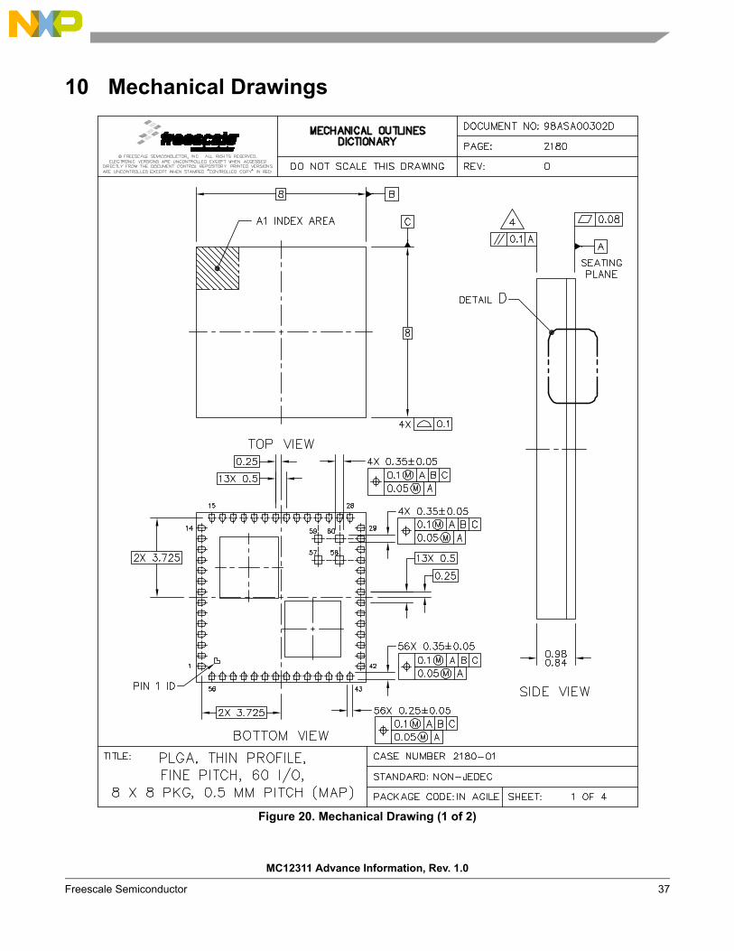
10 Mechanical Drawings
Figure 20. Mechanical Drawing (1 of 2)

MC12311 Advance Information, Rev. 1.0
38 Freescale Semiconductor
Figure 21. Mechanical Drawing (2 of 2)

NOTES
MC12311 Advance Information, Rev. 1.0
Freescale Semiconductor 39

Document Number: MC12311Rev. 1.011/2011
How to Reach Us:
Home Page:www.freescale.com
E-mail:[email protected]
USA/Europe or Locations Not Listed:Freescale SemiconductorTechnical Information Center, CH3701300 N. Alma School RoadChandler, Arizona 85224+1-800-521-6274 or [email protected]
Europe, Middle East, and Africa:Freescale Halbleiter Deutschland GmbHTechnical Information CenterSchatzbogen 781829 Muenchen, Germany+44 1296 380 456 (English)+46 8 52200080 (English)+49 89 92103 559 (German)+33 1 69 35 48 48 (French)[email protected]
Japan:Freescale Semiconductor Japan Ltd.HeadquartersARCO Tower 15F1-8-1, Shimo-Meguro, Meguro-ku,Tokyo 153-0064, Japan0120 191014 or +81 3 5437 [email protected]
Asia/Pacific:Freescale Semiconductor Hong Kong Ltd.Technical Information Center2 Dai King StreetTai Po Industrial EstateTai Po, N.T., Hong Kong+800 2666 [email protected]
For Literature Requests Only:Freescale Semiconductor Literature Distribution CenterP.O. Box 5405Denver, Colorado 802171-800-521-6274 or 303-675-2140Fax: [email protected]
Information in this document is provided solely to enable system and software implementers to use Freescale Semiconductor products. There are no express or implied copyright licenses granted hereunder to design or fabricate any integrated circuits or integrated circuits based on the information in this document.Freescale Semiconductor reserves the right to make changes without further notice to any products herein. Freescale Semiconductor makes no warranty, representation or guarantee regarding the suitability of its products for any particular purpose, nor does Freescale Semiconductor assume any liability arising out of the application or use of any product or circuit, and specifically disclaims any and all liability, including without limitation consequential or incidental damages. “Typical” parameters that may be provided in Freescale Semiconductor data sheets and/or specifications can and do vary in different applications and actual performance may vary over time. All operating parameters, including “Typicals”, must be validated for each customer application by customer’s technical experts. Freescale Semiconductor does not convey any license under its patent rights nor the rights of others. Freescale Semiconductor products are not designed, intended, or authorized for use as components in systems intended for surgical implant into the body, or other applications intended to support or sustain life, or for any other application in which the failure of the Freescale Semiconductor product could create a situation where personal injury or death may occur. Should Buyer purchase or use Freescale Semiconductor products for any such unintended or unauthorized application, Buyer shall indemnify and hold Freescale Semiconductor and its officers, employees, subsidiaries, affiliates, and distributors harmless against all claims, costs, damages, and expenses, and reasonable attorney fees arising out of, directly or indirectly, any claim of personal injury or death associated with such unintended or unauthorized use, even if such claim alleges that Freescale Semiconductor was negligent regarding the design or manufacture of the part.
Freescale™ and the Freescale logo are trademarks of Freescale Semiconductor, Inc. All other product or service names are the property of their respective owners.
© Freescale Semiconductor, Inc. 2010, 2011. All rights reserved.


