
Measuring Vgs on Wide Bandgap Semiconductors ––APPLICATION NOTE
2 | WWW.TEK.COM
APPLICATION NOTEMeasuring Vgs on Wide Bandgap Semiconductors
This application note focuses on accurate high-side VGS
measurements using the IsoVu measurement system. The
measurements described in this application note are shown
on a half-bridge configuration with eGaN FETs on both
the high-side and low-side switches. While high-side gate
measurements are the focus of this application note, the low-
side gate will also be examined.
This application note addresses measurements during the
following events:
1. High-side Turn-on
2. Hide-side Turn-off / Low-side Turn-on
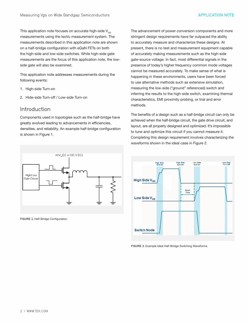
IntroductionComponents used in topologies such as the half-bridge have
greatly evolved leading to advancements in efficiencies,
densities, and reliability. An example half-bridge configuration
is shown in Figure 1.
The advancement of power conversion components and more
stringent design requirements have far outpaced the ability
to accurately measure and characterize these designs. At
present, there is no test and measurement equipment capable
of accurately making measurements such as the high-side
gate-source voltage. In fact, most differential signals in the
presence of today’s higher frequency common mode voltages
cannot be measured accurately. To make sense of what is
happening in these environments, users have been forced
to use alternative methods such as extensive simulation,
measuring the low-side (“ground” referenced) switch and
inferring the results to the high-side switch, examining thermal
characteristics, EMI proximity probing, or trial and error
methods.
The benefits of a design such as a half-bridge circuit can only be
achieved when the half-bridge circuit, the gate drive circuit, and
layout, are all properly designed and optimized. It’s impossible
to tune and optimize this circuit if you cannot measure it.
Completing this design requirement involves characterizing the
waveforms shown in the ideal case in Figure 2.
FIGURE 1. Half-Bridge Configuration.
FIGURE 2. Example Ideal Half-Bridge Switching Waveforms.
WWW.TEK.COM | 3
APPLICATION NOTEMeasuring Vgs on Wide Bandgap Semiconductors
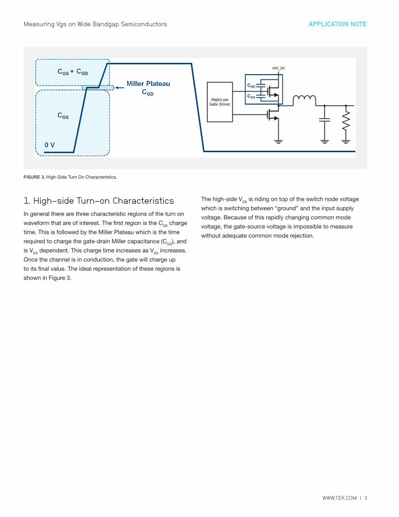
1. High-side Turn-on CharacteristicsIn general there are three characteristic regions of the turn on
waveform that are of interest. The first region is the CGS charge
time. This is followed by the Miller Plateau which is the time
required to charge the gate-drain Miller capacitance (CGD), and
is VDS dependent. This charge time increases as VDS increases.
Once the channel is in conduction, the gate will charge up
to its final value. The ideal representation of these regions is
shown in Figure 3.
The high-side VGS is riding on top of the switch node voltage
which is switching between “ground” and the input supply
voltage. Because of this rapidly changing common mode
voltage, the gate-source voltage is impossible to measure
without adequate common mode rejection.
FIGURE 3. High-Side Turn On Characteristics.
4 | WWW.TEK.COM
APPLICATION NOTEMeasuring Vgs on Wide Bandgap Semiconductors
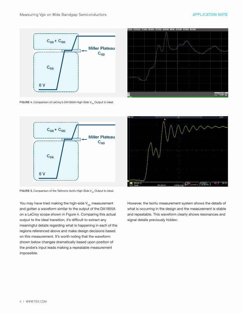
You may have tried making the high-side VGS measurement
and gotten a waveform similar to the output of the DA1855A
on a LeCroy scope shown in Figure 4. Comparing this actual
output to the ideal transition, it’s difficult to extract any
meaningful details regarding what is happening in each of the
regions referenced above and make design decisions based
on this measurement. It’s worth noting that the waveform
shown below changes dramatically based upon position of
the probe’s input leads making a repeatable measurement
impossible.
However, the IsoVu measurement system shows the details of
what is occurring in the design and the measurement is stable
and repeatable. This waveform clearly shows resonances and
signal details previously hidden.
FIGURE 4. Comparison of LeCroy’s DA1855A High-Side VGS Output to Ideal.
FIGURE 5. Comparison of the Tektronix IsoVu High-Side VGS Output to Ideal.

WWW.TEK.COM | 5
APPLICATION NOTEMeasuring Vgs on Wide Bandgap Semiconductors
Until now, the LeCroy DA1855A with a 12-bit oscilloscope has
offered the most insight into these kinds of measurements.
With this measurement system, the user may have been
tempted to optimize their design based on the waveform
information. After all, it does seem to show some of the
expected characteristics. However, the IsoVu system tells a
very different story. Figure 6 shows a comparison of these two
measurement systems and reveals how optimizing based on a
measurement system with limited CMRR and bandwidth can
cause users to severely mis-tune their design.
IsoVu offers users the resolution and repeatability required to
optimize the performance of their designs. As you can see in
Figure 7, there is clear correlation between the Miller plateau
and the switch node transition.
Although the low-side switch is supposed to be “ground”
referenced, it’s interesting to see the actual waveform and
how it may affect the high-side performance. Figure 8 shows
that the low-side switch has ringing due to parasitic coupling
between the low-side switch, the high-side gate and the switch
node.
FIGURE 6. Comparison of Waveforms on a LeCroy Oscilloscope with IsoVu Waveform Overlaid.
FIGURE 8. Interaction of the High-Side and Low-side Switches.
FIGURE 7. High-Side VGS Turn On and Switch Node Compared to Ideal.

6 | WWW.TEK.COM
APPLICATION NOTEMeasuring Vgs on Wide Bandgap Semiconductors
2. High-side Turn-off / Low-side Turn-on CharacteristicsMany of the same characteristics are apparent during the
high-side turn-off/low-side turn on transitions. As shown in
Figure 9, the Miller plateau on the low-side VGS is clearly visible.
The coupling due to parasitics between the switch node
and the high and low-side FETs is apparent, and the IsoVu
measurement system has more than adequate bandwidth to
measure the dead time.
Accurate measurement of the time aligned high-side and low-
side events is critical to avoid simultaneous conduction of the
two FETs which can lead to excess switch loss, efficiency loss
and device degradation.
ConclusionTo accurately make difficult measurements such as the high-
side VGS measurement, you need a measurement system
which combines high bandwidth, high common mode voltage,
and high common mode rejection. Along with its complete
galvanic isolation, the Tektronix IsoVu system offers 1 GHz
bandwidth, 2000 V common mode voltage and 1 Million to 1
(120 dB) common mode rejection ratio. It’s the combination
of these specifications which makes these kinds of difficult
measurements possible.
FIGURE 9. High-Side Turn Off, Low-Side Turn On, and Dead Time.

WWW.TEK.COM | 7
APPLICATION NOTEMeasuring Vgs on Wide Bandgap Semiconductors
Contact Information: Australia* 1 800 709 465
Austria 00800 2255 4835
Balkans, Israel, South Africa and other ISE Countries +41 52 675 3777
Belgium* 00800 2255 4835
Brazil +55 (11) 3759 7627
Canada 1 800 833 9200
Central East Europe / Baltics +41 52 675 3777
Central Europe / Greece +41 52 675 3777
Denmark +45 80 88 1401
Finland +41 52 675 3777
France* 00800 2255 4835
Germany* 00800 2255 4835
Hong Kong 400 820 5835
India 000 800 650 1835
Indonesia 007 803 601 5249
Italy 00800 2255 4835
Japan 81 (3) 6714 3010
Luxembourg +41 52 675 3777
Malaysia 1 800 22 55835
Mexico, Central/South America and Caribbean 52 (55) 56 04 50 90
Middle East, Asia, and North Africa +41 52 675 3777
The Netherlands* 00800 2255 4835
New Zealand 0800 800 238
Norway 800 16098
People’s Republic of China 400 820 5835
Philippines 1 800 1601 0077
Poland +41 52 675 3777
Portugal 80 08 12370
Republic of Korea +82 2 6917 5000
Russia / CIS +7 (495) 6647564
Singapore 800 6011 473
South Africa +41 52 675 3777
Spain* 00800 2255 4835
Sweden* 00800 2255 4835
Switzerland* 00800 2255 4835
Taiwan 886 (2) 2656 6688
Thailand 1 800 011 931
United Kingdom / Ireland* 00800 2255 4835
USA 1 800 833 9200
Vietnam 12060128
* European toll-free number. If not accessible, call: +41 52 675 3777
Find more valuable resources at TEK.COM
Copyright © Tektronix. All rights reserved. Tektronix products are covered by U.S. and foreign patents, issued and pending. Information in this publication supersedes that in all previously published material. Specification and price change privileges reserved. TEKTRONIX and TEK are registered trademarks of Tektronix, Inc. All other trade names referenced are the service marks, trademarks or registered trademarks of their respective companies. 07.16 EA 53W-60779-0


