
Electronics Corp.
Multi-Layer Ceramic Capacitor C-G1-7-00
Darfon Product Specification 1
General Specification
General introduction:
Ceramic capacitors (or condenser) are widely used in electronic circuitry for coupling, de-coupling and in filters.
These different functions require specific capacitor properties. Ceramic capacitors can be divided into two classes,
Class 1
In these capacitors dielectric materials are used which have a very high specific resistance, very good Q and linear
temperature dependence.
They are used in such applications as oscillators and filters where low losses, capacitance drift compensation and
high stability are required.
Class 2
These capacitors have higher losses and have non-linear characteristics. They are used for coupling and
de-coupling.
Construction:
The capacitance of a ceramic capacitor depends on the area of the electrodes (A), the thickness of the ceramic
dielectric (t) and the dielectric constant of the ceramic material (εr ) ; and on the number of dielectric layers (n) with
multi-layer ceramic capacitors :
C =εr ε0 A/t n
The standard capacitance unit is the “Farad”. A capacitor has capacitance of one farad is when one coulomb charges
two parallel conductive plate to one volt potential.
The rated voltage is dependent on the dielectric strength, which is mainly governed by the thickness of the dielectric
layer and the ceramic structure. For this reason a reduction of the layer thickness is limited. Figure 1 shows the
construction of a multi-layer capacitor.
The electrodes are normally mixed palladium with silver since the electrodes are applied before the ceramic is fired
at a temperature where silver would oxidize.
Manufacturing of ceramic capacitors
The raw materials are finely milled and carefully mixed. Thereafter the powders are calcined at temperatures
between 1100 and 1300 to achieve the required chemical composition.
Then, the resultant mass is reground and dopes and/or sintering means are added.
The finely ground material is mixed with a solvent and binding matter. Casting or rolling obtains thin sheets. For
multi-layer capacitors electrode material is printed on the sheets and after stacking and pressing of the sheets
co-fired with the ceramic compact at temperatures between 1000 and 1400.
The totally enclosed electrodes of a multi-layer capacitor guarantee good life test behavior as well.
G 1
Electronics Corp.
Multi-Layer Ceramic Capacitor C-G1-7-00
Darfon Product Specification 2
Operating Voltage
The operating voltage for the capacitors must always be lower than its rated voltage. If an AC voltage is applied, the
peak voltage should be lower than the rated voltage of the capacitor. And if both AC and a pulse voltage may be
presented, then the sum of the peak should also be lower than the rated voltage of the capacitor chosen.
E Standard Number
E 3 1.0 2.2 4.7
E 6 1.0 1.5 2.2 3.3 4.7 6.8
E12 1.0 1.2 1.5 1.8 2.2 2.7 3.3 3.9 4.7 5.6 6.8 8.2
E24 1.0 1.1 1.2 1.3 1.5 1.6 1.8 2.0 2.2 2.4 2.7 3.0 3.3 3.6 3.9 4.3 4.7 5.1 5.6 6.2 6.8 7.5 8.2 9.1
* Non-standard capacitance is available on request.
Available Tolerance
T. C. Capacitance * Standard ToleranceAvailable Tolerance
on Request
Cap < 5pF C = ± 0.25pF
D = ± 0.5pF B = ± 0.1pF
5pF ≦ Cap < 10pF D = ± 0.5pF B = ± 0.1pF
C = ± 0.25pF NP0 (C0G)
Cap ≧ 10pF
E12
J = ± 5%
K = ±10%
F = ± 1%
G = ± 2%
X5R
X7R E6
K = ± 10%
M = ± 20% J = ± 5%
Y5V E3 Z = -20% to +80% M = ± 20%
* Non-standard capacitance is available on request.
G 1

Electronics Corp.
Multi-Layer Ceramic Capacitor C-G1-7-00
Darfon Product Specification 3
Physical Outline
Temperature Compensation
Class I
High Permittivity
Class II Code
Material Type
Elements NME* BME* NME* BME*
1 Dielectric TiO2 CaZrO3 BaTiO3 BaTiO3
2 Electrode PdAg Ni PdAg Ni
3 Ag Cu Ag Cu
4 Ni
5
Termination**
Sn
* NME (Nobel Metal Electrode), BME (Base Metal Electrode)
** All Darfon’s MLCC products are produced under lead-free plating process and in compliance with the
lead-free requirement of Green Plan and ROHS.
(1) Dielectric (4) Ni
(5) Sn
Termination (3) Ag or Cu (2) Electrode, PdAg or Ni
G 1

Electronics Corp.
Multi-Layer Ceramic Capacitor C-G1-7-00
Darfon Product Specification 4
Dimensions
TYPICAL TOLERANCE SIZE CODE L W T g A
(EIA) (Length) (Width) (Max Thickness) (Min) (Termination Min/Max)UNIT
0603 0.6+/-0.03 0.3+/-0.03 0.33 0.15 0.10/0.20 mm
(0201) (0.024+/-0.001) (0.012+/-0.001) (0.013) (0.006) (0.004/0.008) (inch)
1005 1.0 +/- 0.05 0.5 +/- 0.05 0.55 0.30 0.10 / 0.30 mm
(0402) (0.040 +/- 0.002) (0.020 +/- 0.002) (0.022) (0.012) (0.004 / 0.012) (inch)
1608 1.6 +/- 0.10 0.8 +/- 0.10 0.90 0.50 0.25 / 0.65 mm
(0603) (0.063 +/- 0.004) (0.031 +/- 0.004) (0.035) (0.020) (0.010 / 0.026) (inch)
2012 2.0 +/- 0.15 1.25 +/- 0.20 1.45 0.70 0.25 / 0.75 mm
(0805) (0.079 +/- 0.006) (0.049 +/- 0.008) (0.057) (0.028) (0.010 / 0.030) (inch)
3216 3.2 +/- 0.15 1.6 +/- 0.20 1.80 1.50 0.25 / 0.75 mm
(1206) (0.126 +/- 0.006) (0.063 +/- 0.008) (0.069) (0.060) (0.010 / 0.030) (inch)
3225 3.2 +/- 0.20 2.5 +/- 0.20 2.70 1.50 0.25 / 0.75 mm
(1210) (0.126 +/- 0.008) (0.098 +/- 0.008) (0.106) (0.060) (0.010 / 0.030) (inch)
SPECIAL TOLERANCE SIZE CODE L W T g A
(EIA) (Length) (Width) (Max Thickness) (Min) (Termination Min/Max)UNIT
1005* 1.0 +/- 0.15 0.5 +/- 0.15 0.65 0.30 0.10 / 0.30 mm
(0402) (0.040 +/- 0.006) (0.020 +/- 0.006) (0.026) (0.012) (0.004 / 0.012) (inch)
1608* 1.6 + 0.15/-0.1 0.8 + 0.15/-0.1 0.95 0.50 0.25 / 0.65 mm
(0603) (0.063 +0.006/- 0.004) (0.031 +0.006/-0.004) (0.037) (0.020) (0.010 / 0.026) (inch)
2012* 2.0 +/- 0.20 1.25 -0.20/+0.30 1.55 0.70 0.25 / 0.75 mm
(0805) (0.079 +/- 0.008) (0.049 -0.008/+0.012) (0.061) (0.028) (0.010 / 0.030) (inch)
3216* 3.2 +/- 0.20 1.6 -0.20/+0.30 1.90 1.50 0.25 / 0.75 mm
(1206) (0.126 +/- 0.008) (0.063 -0.008/+0.012) (0.075) (0.060) (0.010 / 0.030) (inch)
3225* 3.2 +/- 0.30 2.5 +/- 0.30 2.80 1.50 0.25 / 0.75 mm
(1210) (0.126 +/- 0.012) (0.098 +/- 0.012) (0.11) (0.060) (0.010 / 0.030) (inch)
G 1
L
T
W
A
g

Electronics Corp.
Multi-Layer Ceramic Capacitor C-G1-7-00
Darfon Product Specification 5
DARFON Part Number
C 1005 NP0 101 J G T S
PRODUCT CODE
C = Capacitor SMD
SIZE in mm (EIA CODE, in inch)
0402(01005) 0603(0201) 1005 (0402) 1608 (0603) 2012 (0805) 3216 (1206) 3225(1210) 4520 (1808) 4532 (1812)
T. C.
NP0: 0 ± 30ppm/ -55 to +125 X7R: ±15% -55 to +125 X5R: ±15% -55 to +85 Y5V: +22%/-82% -30 to +85
CAPACITANCE CODE
Expressed in pico-farads and identified by a three-digit number. First two digits represent significant figures. Last digit specifies the number of zeros. (Use 9 for 1.0 through 9.9pF; Use 8 for 0.2 through 0.99pF) (Example: 2.2pF=229 or 0.47pF=478)
TOLERANCE CODE
A: ± 0.05pF B: ± 0.1pF C: ± 0.25pF D: ± 0.5pF F: ±1% G: ±2% J: ±5% K: ±10% M: ±20% Z: +80/-20%
VOLTAGE CODE
B: 4V C: 6.3V D: 10V E: 16V F: 25V N: 35V G: 50V H: 100V J: 200V K: 250V L: 500V M: 630V P: 1KV Q: 2KV R: 3KV S: 4KV
PACKAGING CODE
T: Paper tape reel Ø180mm (7”) P: Embossed tape reel Ø180mm (7”) N: Paper tape reel Ø250mm (10”) D: Embossed tape reel Ø250mm (10”) A: Paper tape reel Ø330mm (13”) E: Embossed tape reel Ø330mm (13”) B: Bulk, loosed in bag C: Bulk cassette W: Special Packing
Product Type
S: Standard Ceramic Capacitor Q: High Q/Low ESR
G 1

Electronics Corp.
Multi-Layer Ceramic Capacitor C-G1-7-00
Darfon Product Specification 6
Product Range
NP0 (Class I)
Type Size
T.C. RV 0603 (0201) 1005 (0402) 1608 (0603) 2012 (0805) 3216 (1206)
16V 2.7nF~3.3nF 12nF~39nF
25V 0.20pF~100pF 0.20pF~22pF
50V 0.20pF~18pF 0.20pF~470pF/1nF 0.20pF~2.2nF 0.50pF~10nF 1.50pF~10nF
NPO
Class I
100V 0.20pF~220pF 0.20pF~1nF 0.50pF~3.3nF 1.50pF~4.7nF
X7R (Class II)
Type Size
T.C. RV 0603 (0201) 1005 (0402) 1608 (0603) 2012 (0805) 3216 (1206) 3225 (1210)
6.3V 4.7uF~10uF
10V 3.3nF/4.7nF/10nF 100pF~100nF 100pF~1uF 1uF/2.2uF/4.7uF/10uF 2.2uF
16V 100pF~100nF 100pF~1uF 330nF/470nF/1uF/ 2.2uF 470nF~10uF 10uF
25V 100pF~2.2nF 100pF~22nF 100pF~1uF 1nF~1uF 220nF~4.7uF 4.7uF/10uF
50V 100pF~2.2nF 100pF~10nF 100pF~100nF 150pF~470nF 1nF~1uF
X7R
Class II
100V 100pF~10nF 150pF~22nF 1nF~100nF
X5R (Class II)
Type Size
T.C. RV 0603 (0201) 1005 (0402) 1608 (0603) 2012 (0805) 3216 (1206) 3225 (1210)
6.3V 2.2nF~220nF 470nF~4.7uF 2.2uF/ 4.7uF/10uF 4.7uF~22uF 22uF/47uF 47uF/100uF
10V 2.2nF~100nF 15nF~1uF 220nF~4.7uF 2.2uF~10uF 2.2uF~10uF 22uF
16V 15nF~1uF 220nF~2.2uF 1uF~10uF 2.2uF~10uF 4.7uF~22uF
X5R
Class
II 25V 100nF 220nF/1uF 1uF~4.7uF 2.2uF~10uF 4.7uF/ 10uF
Y5V (Class II)
Type Size
T.C. RV 0603 (0201) 1005 (0402) 1608 (0603) 2012 (0805)
6.3V 22nF~100nF 10nF~1uF 10nF~2.2uF
10V 10nF~1uF 10nF~2.2uF
16V 10nF~220nF 10nF~2.2uF 100nF~2.2uF
25V 10nF~100nF 10nF~330nF 100nF ~2.2uF
Y5V
Class II
50V 10nF~33nF 10nF~220nF 100nF~1uF
Note:(1) Other size, capacitance, and voltage are available upon customer’s request.
(2) Product range might be extended due to technology improvement or new product released;for up-to-date information,
please contact our sales.
(3) Part of Y5V product will be phased out.
G 1

Electronics Corp.
Multi-Layer Ceramic Capacitor C-G1-7-00
Darfon Product Specification 7
Packaging
Tape and Reel Packaging
Tape and reel packaging is currently the most promising system for high-speed production. A typical 180mm (7
inch) diameter reel contains 1,500 to 15,000 capacitors, 250mm (10 inch) contains 10,000 capacitors, and
330mm(13 inch) contains 10,000 to 50,000 capacitors. Three standard sizes are available in taped and reeled
package either with paper carrier tapes or embossed tapes.
Reel Specifications
TAPE WIDTH
(mm)
G
(mm)
T max.
(mm)
D
(mm)
8 10.0 +/- 1.5 14.5 180
8 10.0 +/- 1.5 14.5 250
8 10.0 +/- 1.5 14.5 330
12 14.0 +/- 1.5 18.5 180
2.0+/-0.5
13.0+/-0.5 21.0+/-0.8
50 m
in.
D
10.0+/-1.5 for 8mm wide tape 14.0+/-1.5 for 12mm wide tape
G
T
Electronics Corp.
Multi-Layer Ceramic Capacitor C-G1-7-00
Darfon Product Specification 8
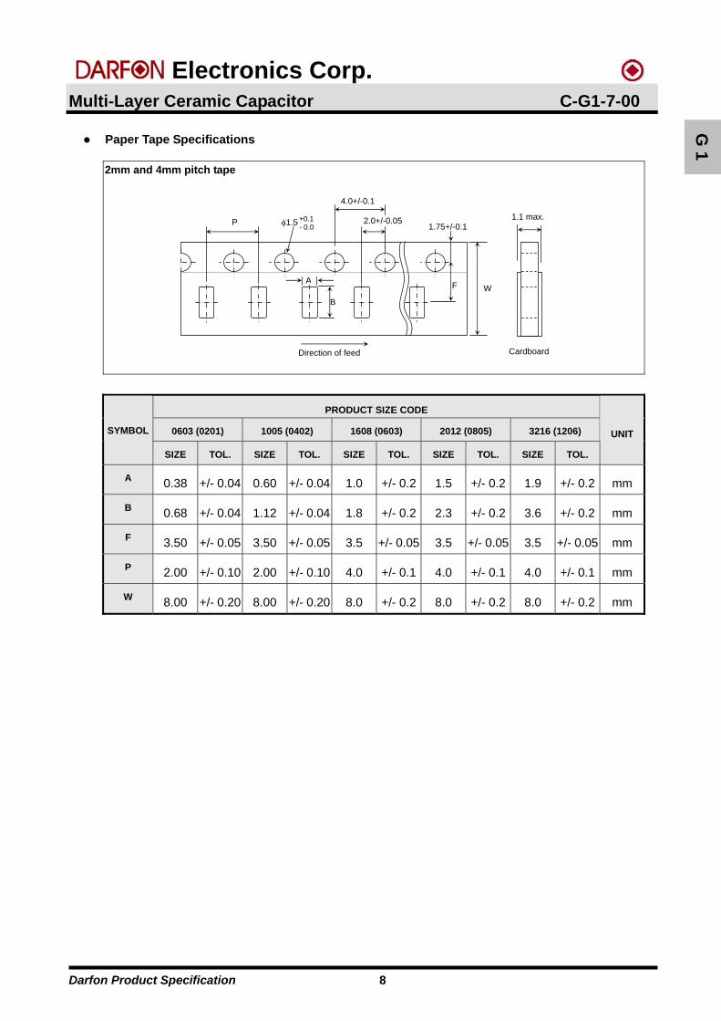
Paper Tape Specifications
2mm and 4mm pitch tape
PRODUCT SIZE CODE
0603 (0201) 1005 (0402) 1608 (0603) 2012 (0805) 3216 (1206) SYMBOL
SIZE TOL. SIZE TOL. SIZE TOL. SIZE TOL. SIZE TOL.
UNIT
A 0.38 +/- 0.04 0.60 +/- 0.04 1.0 +/- 0.2 1.5 +/- 0.2 1.9 +/- 0.2 mm
B 0.68 +/- 0.04 1.12 +/- 0.04 1.8 +/- 0.2 2.3 +/- 0.2 3.6 +/- 0.2 mm
F 3.50 +/- 0.05 3.50 +/- 0.05 3.5 +/- 0.05 3.5 +/- 0.05 3.5 +/- 0.05 mm
P 2.00 +/- 0.10 2.00 +/- 0.10 4.0 +/- 0.1 4.0 +/- 0.1 4.0 +/- 0.1 mm
W 8.00 +/- 0.20 8.00 +/- 0.20 8.0 +/- 0.2 8.0 +/- 0.2 8.0 +/- 0.2 mm
B
A
P
4.0+/-0.1
2.0+/-0.051.75+/-0.11.5
+0.1- 0.0
W
Direction of feed
1.1 max.
F
Cardboard
G 1

Electronics Corp.
Multi-Layer Ceramic Capacitor C-G1-7-00
Darfon Product Specification 9
Embossed Tape Specifications
4mm and 8mm pitch tape
ko: so chosen that the orientation of the component cannot change.
For W= 8mm: T2=2.5mm max.
For W= 12mm: T2= 4.5mm
PRODUCT SIZE CODE
4 mm tape 8 mm tape DIMENSION
(mm) 2012 (0805) 3216 (1206) 3225 (1210) 4520 (1808) 4532 (1812)
TOLERANCE
(mm)
P1 4 4 4 8 8 +/- 0.10
PO 4 4 4 4 4 +/- 0.10
P2 2 2 2 2 2 +/- 0.05
A0 nominal clearance* 0.2 0.3 0.3 0.4 0.4 -
B0 nominal clearance* 0.2 0.3 0.3 0.4 0.4 -
K0 minimum clearance* 0.05 0.05 0.05 0.05 0.05 -
W 8.0 8.0 8.0 12.0 12.0 +/- 0.20
E 1.75 1.75 1.75 1.75 1.75 +/- 0.10
F 3.5 3.5 3.5 5.5 5.5 +/- 0.05
D0 1.5 1.5 1.5 1.5 1.5 +0.1/-0.0
D1 1 min 1 min 1 min 1.5 min 1.5 min +0.1/-0.0
T 0.25 0.25 0.25 0.25 0.25 +/- 0.10
T1 0.05 0.05 0.05 0.05 0.05 +/- 0.01
T2 2.5 max. 2.5 max. 2.5 max. 4.5 4.5 -
* Typical capacitors displace in pocket.
B0
A0
P1
P0
P2 E
W
Direction of feed
F
D0
D1
T1
T2
K0
T
Top tape
G 1

Electronics Corp.
Multi-Layer Ceramic Capacitor C-G1-7-00
Darfon Product Specification 10
Thickness and Taping Amount
Amount per reel Thickness
180 mm (7”) 250 mm (10”) 330 mm (13”) Code Spec Size(EIA) Paper Embossed Paper Embossed Paper Embossed
A 0.30+/-0.03 0603 (0201) 15K B 0.50+/-0.05 1005 (0402) 10K 50K B 0.50+/-0.15 1005 (0402) 10K 50K Q 0.45+/-0.05 1005 (0402) 10K 50K
2012 (0805) 4K 10K 15K C 0.60+/-0.15
3216(1206) 4K 10K 15K Q 0.45+/-0.05 1608(0603) 4K 10K 15K D 0.80+/-0.10 1608(0603) 4K 10K 15K D 0.80+0.15/ -0.10 1608 (0603) 4K 10K 15K
2012 (0805) 4K 10K 15K 3216 (1206) 4K 10K 15K 3225 (1210) 3K 10K
E 0.85+/-0.15
4532 (1812) 1K 2012(0805) 3K
I 0.95+/-0.15 3216(1206) 3K 3216 (1206) 3K 10K
F 1.15+/-0.20 4520 (1808) 3K 2012 (0805) 2K/3K 10K 3216 (1206) 3K 10K 3225 (1210) 3K 4520(1808) 3K
G 1.25 +/-0.20
4532(1812) 1K 2012(0805) 2K/3K 10K 3216(1206) 3K 10K G 1.25+0.3/-0.2 3225(1210) 3K 3216(1206) 2K 3225(1210) 2K 4520(1808) 2K
L 1.60+/-0.20
4532(1812) 1K 3216(1206) 2K 3225(1210) 2K 4520(1808) 2K
L 1.60+0.30/-0.20
45321812) 1K 3216 (1206) 2K/3K 3225 (1210) 2K 4520 (1808) 1K
N 2.00+/-0.20
4532(1812) 1K N 2.00+/-0.30 3225 (1210) 2K P 2.50+/-0.20 3225(1210) 500pcs/1K P 2.50+/-0.30 3225(1210) 500pcs/1K
G 1
Electronics Corp.
Multi-Layer Ceramic Capacitor C-G1-7-00
Darfon Product Specification 11
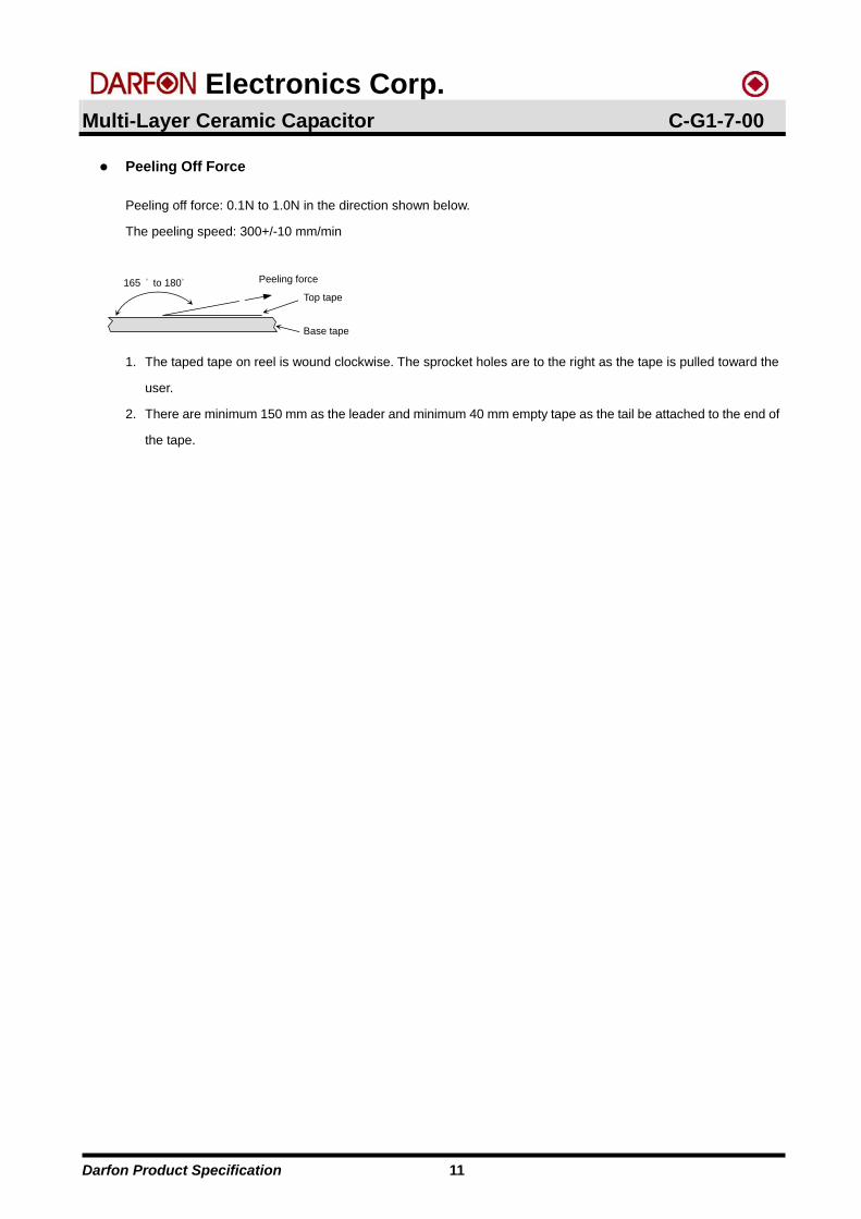
Peeling Off Force
Peeling off force: 0.1N to 1.0N in the direction shown below.
The peeling speed: 300+/-10 mm/min
1. The taped tape on reel is wound clockwise. The sprocket holes are to the right as the tape is pulled toward the
user.
2. There are minimum 150 mm as the leader and minimum 40 mm empty tape as the tail be attached to the end of
the tape.
Top tape
Base tape
Peeling force165 ° to 180°
Electronics Corp.
Multi-Layer Ceramic Capacitor C-S2-7-00
Darfon Product Specification 1 Rev.: 6
X5R, X7R Dielectrics Features
A monolithic structure ensures high reliability and mechanical strength.
High capacitance density.
A wide range of capacitance values in standard case size.
Suitable for high speed SMT placement on PCBs.
Ni barrier termination highly resistance to migration.
Lead-free termination is in compliance with the requirement of green plan and ROHS.
Applications
General electronic equipment.
Communication equipment.
Custom Application
X5R, X7R Dielectric Characteristics
Capacitance Range 100pF to 100uF
Size (mm)
(EIA inch)
0603 1005 1608 2012 3216 3225
(0201) (0402) (0603) (0805) (1206) (1210)
Test Voltage 1.0 ± 0.2Vrms
Test Frequency 1.0 ± 0.2KHz
Capacitance Tolerance ± 10%, ± 20% (± 5% available on request)
Operating Temperature Range -55 to +85 for X5R
-55 to +125 for X7R
Maximum Capacitance Change ± 15 %
Rated Voltage 6.3, 10, 16, 25, 50, 100 VDC
Dissipation Factor Pls refer to DF table on page No. 7
Insulation Resistance (+25, RVDC) 10,000 M min. or 500-F min., whichever is smaller
Insulation Resistance (Maximum
operating temperature, RVDC)
1,000 M min. or 50-F min., whichever is smaller
S 2

Electronics Corp.
Multi-Layer Ceramic Capacitor C-S2-7-00
Darfon Product Specification 2 Rev.: 6
Product Range and Thickness
CLASS Class II TYPE Standard T.C. X7R SIZE 0603 1005 1608 2012 3216 3225 (EIA) 0201 0402 0603 0805 1206 1210 RV 10V 16V 25V 50V 10V 16V 25V 50V 10V 16V 25V 50V 100V 6.3V 10V 16V 25V 50V 100V 10V 16V 25V 50V 100V 16V 25V
100 p A A B B B B D D D D D
120 p A A B B B B D D D D D
150 p A A B B B B D D D D D C E E
180 p A A B B B B D D D D D C E E
220 p A A B B B B D D D D D C E E
270 p A A B B B B D D D D D C E E
330 p A A B B B B D D D D D C E E
390 p A A B B B B D D D D D C E E
470 p A A B B B B D D D D D C E E
560 p A A B B B B D D D D D C E E
680 p A A B B B B D D D D D C E E
820 p A A B B B B D D D D D C E E
1.0 n A A B B B B D D D D D C E C E E E E
1.2 n A A B B B B D D D D D C E C E E E E
1.5 n A A B B B B D D D D D C E C E E E E
1.8 n A A B B B B D D D D D C E C E E E E
2.2 n A A B B B B D D D D D C E C E E E E
2.7 n B B B B D D D D D C E C E E E E
3.3 n A B B B B D D D D D C E C E E E E
3.9 n B B B B D D D D D C E C E E E E
4.7 n A B B B B D D D D D C E C E E E E
5.6 n B B B B D D D D D C E C E E E E
6.8 n B B B B D D D D D C E C E E E E
8.2 n B B B B D D D D D C E C E E E E
10 n A B B B B D D D D D C E C E E E E
12 n B B B D D D D C E C E E E E
15 n B B B D D D D C E C E E E E
18 n B B B D D D D C E C E E E E
22 n B B B D D D D C E C E E E E
27 n B B D D D D C E C E E E
33 n B B D D D D* C E C E E E
39 n B B D D D D* C E C E E E
47 n B B D D D D* E E E E
56 n B B D D D D* E E E E
68 n B B D D D D* E E E E
82 n B B D D D D* E E E E G
100 n B B D D D D* E E E E G
120 n E E
150 n E E
180 n E E
220 n D D D* E E I I
270 n
330 n D* D* G G G I G
390 n
470 n D* D* G G G G G L
560 n
680 n
820 n
1.0 u D* D* D* G G G G G G L
1.2 u
1.5 u
1.8 u
2.2 u G G L L L
2.7 u
3.3 u
3.9 u
4.7 u G G L L N10 u G L N N
Non-standard capacitance or thickness is available on request * Special length/width tolerance
The thickness might be changed due to technology improvement.
S 2

Electronics Corp.
Multi-Layer Ceramic Capacitor C-S2-7-00
Darfon Product Specification 3 Rev.: 6
Product Range and Thickness CLAS Class II
TYPE Standard
T.C. X5R
SIZE 0603 1005 1608 2012 3216 3225
(EIA) 0201 0402 0603 0805 1206 1210
RV 6.3V 10V 6.3V 10V 16V 25V 6.3V 10V 16V 25V 6.3V 10V 16V 25V 6.3V 10V 16V 25V 6.3V 10V 16V 25V
2.2 n A A
3.3 n A A
4.7 n A A
5.6 n A A
6.8 n A A
8.2 n A A
10 n A A
15 n B B
22 n A A B B
33 n B B
47 n A A B B
56 n B B
68 n B B
82 n B B
100 n A A B B B
120 n B B
150 n B B
180 n B B
220 n A B B D D D
270 n
330 n D D
390 n
470 n B B D D
560 n
680 n D D
820 n
1.0 u B B B Q D D D E G E G
1.5 u
1.8 u
2.2 u B D D D E G G L L L
2.7 u
3.3 u
3.9 u
4.7 u B* D D G G G G L L L N N
6.8 u
10 u D* G G G L L L N N
22 u G L N P N P
47 u L P
100 u P
Thickness Tolerance
Special Length/Width Tolerance
Size Code(EIA) 1005(0402) 1608(0603) 2012(0805) 3216(1206) 3225(1210) Length(mm) 1.0 ± 0.15 1.6 ± 0.15 2.0 ± 0.20 3.2 ± 0.20 3.2 ± 0.30 Width(mm) 0.5 ± 0.15 0.8 ± 0.15 1.25 ± 0.30 1.6 ± 0.30 2.5 ± 0.30
Thickness (mm) Thickness (mm) Thickness (mm) Thickness (mm) Thickness (mm) Thickness (mm) Code Class Code Class Code Class Code Class Code Code Code Code
A 0.30+/-0.03 C 0.60+/-0.15 E 0.85+/-0.15 G 1.25 -0.20/+0.30 L 1.60+0.3/-0.20 P 2.50+/-0.20 B 0.50+/-0.05 D 0.80+/-0.10 F 1.15+/-0.20 I 0.95+/-0.15 N 2.00+/-0.20 Q 0.45+/-0.05 B 0.50+/-0.15 D 0.8+0.15/-0.1 G 1.25+/-0.20 L 1.60+/-0.20 N 2.00+/-0.30
S 2
Non-standard capacitance or thickness is available on request * Special length/width tolerance
The thickness might be changed due to technology improvement.

Electronics Corp.
Multi-Layer Ceramic Capacitor C-S2-7-00
Darfon Product Specification 4 Rev.: 6
Taping Amount
Amount per reel Thickness
180 mm (7”) 250 mm (10”) 330 mm (13”) Code Spec Size(EIA) Paper Embossed Paper Embossed Paper Embossed
A 0.30+/-0.03 0603 (0201) 15K B 0.50+/-0.05 1005 (0402) 10K 50K B 0.50+/-0.15 1005 (0402) 10K 50K Q 0.45+/-0.05 1005 (0402) 10K 50K
2012 (0805) 4K 10K 15K C 0.60+/-0.15
3216(1206) 4K 10K 15K Q 0.45+/-0.05 1608(0603) 4K 10K 15K D 0.80+/-0.10 1608(0603) 4K 10K 15K D 0.80+0.15/ -0.10 1608 (0603) 4K 10K 15K
2012 (0805) 4K 10K 15K 3216 (1206) 4K 10K 15K 3225 (1210) 3K 10K
E 0.85+/-0.15
4532 (1812) 1K 2012(0805) 3K
I 0.95+/-0.15 3216(1206) 3K 3216 (1206) 3K 10K
F 1.15+/-0.20 4520 (1808) 3K 2012 (0805) 2K/3K 10K 3216 (1206) 3K 10K 3225 (1210) 3K 4520(1808) 3K
G 1.25 +/-0.20
4532(1812) 1K 2012(0805) 2K/3K 10K 3216(1206) 3K 10K G 1.25+0.3/-0.2 3225(1210) 3K 3216(1206) 2K 3225(1210) 2K 4520(1808) 2K
L 1.60+/-0.20
4532(1812) 1K 3216(1206) 2K 3225(1210) 2K 4520(1808) 2K
L 1.60+0.30/-0.20
45321812) 1K 3216 (1206) 2K/3K 3225 (1210) 2K 4520 (1808) 1K
N 2.00+/-0.20
4532(1812) 1K N 2.00+/-0.30 3225 (1210) 2K P 2.50+/-0.20 3225(1210) 500pcs/1K P 2.50+/-0.30 3225(1210) 500pcs/1K
S 2
Electronics Corp.
Multi-Layer Ceramic Capacitor C-S2-7-00
Darfon Product Specification 5 Rev.: 6
X5R, X7R Specifications
Item Specification Test Method
1 Operating Temperature Range X7R: -55 to 125 degree C
X5R: -55 to 85 degree C
---
2 Rated Voltage 6.3VDC, 10VDC, 16VDC, 25VDC, 35VDC, 50VDC, 100VDC, The rated voltage is defined as the maximum voltage, which
may be applied continuously to the capacitor.
3 Appearance No defects or abnormalities. Visual inspection
4 Dimensions Within the specified dimension. Using calipers
5 Dielectric Strength No defects or abnormalities. No failure shall be observed when 250%* of the rated voltage
is applied between the terminations for 1 to 5 seconds. The
charge and discharge current is less than 50mA.
Rated Voltage: <500V To apply rated
voltage. 6 Insulation Resistance ( I.R.)
Rated Voltage: ≧500V To apply 500V.
I.R. ≧10G or
RiCR≧500Ω-F
(whichever is
smaller)
The insulation resistance shall be measured with a DC voltage
not exceeding the rated voltage at 25 and 75%RH max, and
within 1 minute of charging.
7 Capacitance Within the specified tolerance
* X7R, X5R at 1000 hours
I. X5R, X7R:
See X5R,X7R DF table 3
8 Q/Dissipation Factor ( D.F.)
Table 1
Size Thickness TC RV Cap0603 0.3 mm X5R 6.3V 1041005 0.5 mm X5R 4V/6.3V 4751608 0.8 mm X5R 4V/6.3V 106
The capacitance / D.F. shall be measured at 25 at the
frequency and voltage shown in the tables.
Item ClassII
(≦10 uF)
ClassII
(>10 uF)
* For item in
Table1
Frequency 1.0±0.2kHz 120Hz±24Hz 1.0±0.2kHz
Voltage 1.0±0.2Vrms 0.5±0.1Vrms 0.5±0.1Vrms
9 Capacitance Temperature
Characteristics
Capacitance change
X7R/X5R within ±15%
The ranges of capacitance change compared with the 25
value over the temperature ranges shall be within the specified
ranges.
10 Termination Strength No removal of the terminations or marking defect. Apply a parallel force of 5N to a PCB mounted sample for
10±1sec. *2N for 0603 (EIA 0201).
No cracking or marking defects shall occur at 1mm deflection.
Capacitance change:
X7R, X5R:within ±12.5%
Solder the capacitor to the test jig (glass epoxy boards) shown
in Fig.a using a SAC305(Sn96.5Ag3.0Cu0.5) solder (then let sit
for 48±4 hours for X7R X5R and Y5V).
Then apply a force in the direction shown in Fig.b. The
soldering shall be done with the reflow method and shall be
conducted with care so that the soldering is uniform and free of
defects such as heat shock.
11 Deflection (Bending Strength)
Size a b C
0603 0.3 0.9 0.3
1005 0.4 1.5 0.5
1608 1.0 3.0 1.2
2012 1.2 4.0 1.65
3216 2.2 5.0 2.0
4520 3.5 7.0 2.5
4532 3.5 7.0 3.7
12 Solderability of Termination 90% of the terminations are to be soldered evenly and
continuously.
Immerse the test capacitor into a methanol solution containing
rosin for 3 to 5 seconds, preheat it 150 to 180 for 2 to 3
minutes and immerse it into Sn-3.0Ag-0.5Cu solder of 245 ± 5
for 3±1seconds.
20 50
R230
45 45
Pressurizing speed : 1.0mm/sec.
Capacitance Meter
Pressurize
Flexure : 1mm
Fig. b.
b
a
c
t :1.6mm(0.8mm for 0603&1005 size)
40
100
4.5
Fig. a.
S 2

Electronics Corp.
Multi-Layer Ceramic Capacitor C-S2-7-00
Darfon Product Specification 6 Rev.: 6
Continued from previous page.
Item Specification Test Method
Appearance No marking defects
Cap. Change X7R/X5R within ±7.5%
Q/D.F. To satisfy the specified initial spec.
13 Resistance to Soldering Heat
I.R. I.R.≧10,000M or RiCR≧500-F.
(whichever is smaller)
*Preheat the capacitor at 120 to 150 for 1 minute. Immerse the capacitor in a SAC305(Sn96.5Ag3.0Cu0.5) solder solution at 270±5 for 10±1 seconds. Let sit at room
temperature for 24±2 hours (temperature compensating type) or 48±4 hours (high dielectric constant type), then measure. * Preheat 150 to 200 for size ≧3216.
Initial measurement : perform a heat treatment at 150+0/-10
for one hour and then let sit for 48±4 hours at room temperature. Perform the initial measurement.
Appearance No marking defects
Cap. Change X7R/X5R within ±7.5%
Q/D.F. To satisfy the specified initial spec.
14 Temperature cycle (Thermal shock)
I.R. I.R.≧10,000M or RiCR≧500-F.
(whichever is smaller)
Solder the capacitor to supporting jig (glass epoxy board) and perform the five cycles according to the four heat treatments listed in the following table. Let sit for 24±2hrs at room temperature, then measure. Step 1: Minimum operating temperature 30±3min Step 2: Room temperature 2~3 min Step 3: Maximum operating temperature 30±3min Step 4: Room temperature 2~3min
Initial measurement: perform a heat treatment at 150+/-10
for an hour and then let sit for 48±4 hours at room temp. Perform the initial measurement.
Appearance No marking defects
Cap. Change X7R/X5R within ±12.5%
Q/D.F. X7R 200% max of initial spec.
X5R 200% max of initial spec.
15 Humidity load
I.R. I.R.≧500M or RiCR≧25-F.
(whichever is smaller)
* some of the parts are RiCr≧12.5-Fplease refer to table 2
Apply the rated voltage at 40±2 and 90 to 95% humidity for 500±12 hours. Remove and let sit for 24±2 hours (temperature compensating type) or 48±4 hours (high dielectric constant type) at room temperature, then measure.
The charge / discharge current is less than 50mA.
Initial measurement: perform a heat treatment at 150+/-10 for one hour and then let sit for 48±4hours at room temperature. Perform the initial measurement.
Appearance No marking defects
Cap. Change X7R/X5R within ±12.5%
Q/D.F. X7R 200% max of initial value
X5R 200% max of initial value
16 High temperature load life test
I.R. More than 1GΩ or RiCr≧50 -F (whichever is less.)
* some of the parts are RiCr≧25-Fplease refer to table 2
Apply 200% of the rated voltage for 1000±12 hours at the maximum operating temperature ± 3. Let sit for 24± 2 hours (temperature compensating type) or 48±4 hours (high dielectric constant type) at room temperature, then measure.
The charge/discharge current is less than 50mA.
Initial measurement: perform a heat treatment at 150+/-10 for one hour and then let sit for 48±4hours at room temperature. Perform the initial measurement. P.S.: Please refer to table 2 for items applying 150% voltage.
* some of the parts are applicable in rated voltage *1.5. please
refer to table 2
Table 2 TC Product Range
X5R
0603 (EIA 0201): C > 10 nF
1005 (EIA 0402): C > 0.1 uF
1608 (EIA 0603): C ≧ 1.0 uF
2012 (EIA 0805): C ≧ 2.2 uF
3216 (EIA 1206): C ≧ 10 uF
3225 (EIA 1210): C ≧ 22 uF
S 2

Electronics Corp.
Multi-Layer Ceramic Capacitor C-S2-7-00
Darfon Product Specification 7 Rev.: 6
X5R/X7R DF (tan ) Table 3
D.F Max. Rated Voltage Size Capacitance
X5R X7R
4V All All 15.0% All cap ≦1.0uF 10.0% 7.5% All 1.0uF< cap <4.7uF 10.0% 10.0% 6.3V
All 4.7uF≦ cap ≦100uF 15.0% 15.0%
0603/3216/3225 All 7.5% 5.0%
0603 100nF≦ cap 10.0% cap ≦100nF 7.5% 5.0%
100nF< cap <330nF 7.5% 1005
330nF≦ cap 10.0% cap ≦1.0uF 7.5% 5.0%
1.0uF< cap <2.2uF 7.5% 1608
2.2uF≦ cap 10.0% cap <2.2uF 7.5% 5.0%
2012 2.2uF≦ cap 10.0%
3216 10uF 10.0% 10.0%
10V
3225 10uF< cap ≦22uF 10.0% 10.0% 0603/3216/3225 All 5.0% 5.0%
cap ≦100nF 5.0% 5.0% 1005
100nF< cap ≦220nF 7.5% cap ≦470nF 5.0% 5.0%
470nF< cap <1.0uF 7.5% 5.0% 1608
1.0uF≦ cap 10.0% 10.0% cap ≦2.2uF 5.0% 5.0%
2.2uF< cap ≦4.7uF 7.5% 2012
4.7uF< cap ≦10uF 10.0% 3216 4.7uF< cap 10.0% 10.0%
16V
3225 10uF< cap ≦22uF 15.0% All 5.0% 3.5%
All 1.0uF≦ cap 10.0%
1608 470nF 10.0% 1.0uF< cap ≦4.7u 5.0% 5.0%
3216 4.7uF< cap 10.0%
25V
3225 4.7uF< cap ≦10u 10.0% All All but below 2.5% 3.0%
≧50V 3216/3225 cap ≦1.0uF 3.5% 3.5%
S 2
Electronics Corp.
Multi-Layer Ceramic Capacitor C-C1-1-00
Darfon Product Specification 1 Rev.: 0
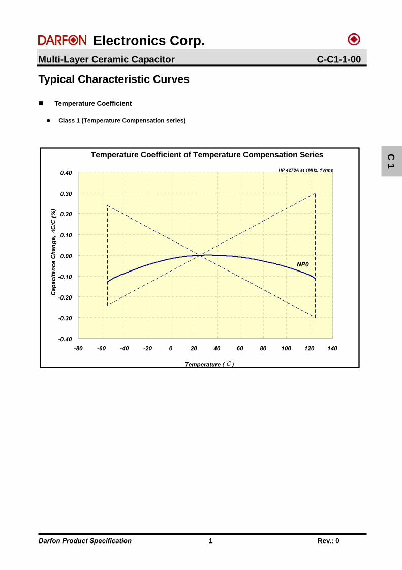
Typical Characteristic Curves
Temperature Coefficient
Class 1 (Temperature Compensation series)
-0.40
-0.30
-0.20
-0.10
0.00
0.10
0.20
0.30
0.40
-80 -60 -40 -20 0 20 40 60 80 100 120 140
Cap
acit
ance
Ch
ang
e,
C/C
(%
)
Temperature ( )
Temperature Coefficient of Temperature Compensation Series
HP 4278A at 1MHz, 1Vrms
NP0
C 1
Electronics Corp.
Multi-Layer Ceramic Capacitor C-C1-1-00
Darfon Product Specification 2 Rev.: 0
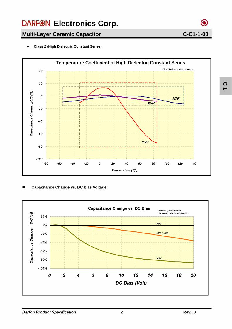
Class 2 (High Dielectric Constant Series)
-100
-80
-60
-40
-20
0
20
40
-80 -60 -40 -20 0 20 40 60 80 100 120 140
Temperature ( )
Ca
pa
cit
an
ce
Ch
an
ge
, C
/C (
%)
Temperature Coefficient of High Dielectric Constant SeriesHP 4278A at 1KHz, 1Vrms
Y5V
X7RX5R
Capacitance Change vs. DC bias Voltage
C 1
-100%
-80%
-60%
-40%
-20%
0%
20%
0 2 4 6 8 10 12 14 16 18 20
Capacitance Change vs. DC Bias
DC Bias (Volt)
HP 4284A, 1MHz for NP0HP 4284A, 1KHz for X5R,X7R,Y5V
Y5V
X7R / X5R
NP0
Ca
pa
cit
an
ce
Ch
an
ge
, C
/C (
%)

Electronics Corp.
Multi-Layer Ceramic Capacitor C-C1-1-00
Darfon Product Specification 3 Rev.: 0
Impedance vs. Frequency
0.01
0.10
1.00
10.00
100.00
1000.00
1 10 100 1000 10000
Typical Impedance |Z| vs. Frequency
Imp
edan
ce (Ω
)
Frequency (MHz)
HP 4287A+16196A, 0.5V
NP0 0603 1pFNP0 0603 100pF
X7R 0603 1nF
X7R 0603 10nF
NP0 0603 10pF
Y5V 0603 0.1uF
C 1

Electronics Corp.
Multi-Layer Ceramic Capacitor C-C1-1-00
Darfon Product Specification 4 Rev.: 0
Aging Rate
C 1
-30.0
-25.0
-20.0
-15.0
-10.0
-5.0
0.0
5.0
10.0
1 10 100 1000 10000 100000
Typical Curve of Aging Rate of D ifferent D ielectric M aterial
Cap
acita
nce
Cha
nge
Per
cent
(%
)
T im e (Hours)
NP0
X7R, X5R
Y5V
Electronics Corp.
Multi-Layer Ceramic Capacitor C-A1-4-00
Darfon Product Specification 1 Rev.: 3
Application Note
Circuit Design
1. Once application and assembly environments have been checked, the capacitor may be used in conformance
with the rating and performance, which are provided in both the catalog and the specifications. Exceeding the
specifications listed may result in inferior performance. It may also cause a short, open, smoking, or flaming to
occur, etc.
2. Please use the capacitors in conformance with the operating temperature provided in both the catalog and the
specifications. Be especially cautious not to exceed the maximum temperature. In the situation the maximum
temperature set forth in both the catalog and specifications is exceeded, the capacitor’s insulation resistance
may deteriorate, power may suddenly surge and short-circuit may occur. The loss of capacitance will occur, and
may self-heat due to equivalent series resistance when alternating electric current is passed through. As this
effect becomes critical in high frequency circuits, please exercise with caution. When using the capacitor in a
(self-heating) circuit, please make sure the surface of the capacitor remains under the maximum temperature for
usage. Also, please make certain temperature rise remain below 20 .
3. Please keep voltage under the rated voltage, which is applied to the capacitor. Also, please make certain the
peak voltage remains below the rated voltage when AC voltage is super-imposed to the DC voltage. In the
situation where AC or pulse voltage is employed, ensure average peak voltage does not exceed the rated
voltage. Exceeding the rated voltage provided in both catalog and specifications may lead to defective
withstanding voltage or, in worse case situations, may cause the capacitor to burn out.
4. It’s is a common phenomenon of high-dielectric products to have a deteriorated amount of static electricity due to
the application of DC voltage.
Storage
1. The chip capacitors shall be packaged in carrier tapes or bulk cases.
2. Keep storage place temperatures from +5 to +35, humidity from 45 to 70% RH.
3. The storage atmosphere must be free of gas containing sulfur and chlorine. Also, avoid exposing the product to
saline moisture. If the product is exposed to such atmospheres, the terminations will oxidize and solderability will
be affected.
4. The solderability is assured for 12 months from our final inspection date if the above storage condition is
followed.

Electronics Corp.
Multi-Layer Ceramic Capacitor C-A1-4-00
Darfon Product Specification 2 Rev.: 3
Handling
Chip capacitors should be handled with care to avoid contamination or damage. The use of vacuum pick-up or
plastic tweezers is recommended for manual placement. Tape and reeled packages are suitable for automatic pick
and placement machine.
Flux
1. An excessive amount of flux or too rapid temperature rise can causes solvent burst, solder can generate a large
quantity of gas. The gas can spreads small solder particles to cause solder balling effect or bridging problem.
2. Flux containing too high of a percentage of halide may cause corrosion of termination unless sufficient cleaning
is applied.
3. Use rosin-type flux. Highly acidic flux (halide content less than 0.2wt%) is not recommended.
4. The water soluble flux causes deteriorated insulation resistance between outer terminations unless sufficiently
cleaned.
Component Spacing
For wave soldering components, the spacing must be sufficient far apart to prevent bridging or shadowing. This is
not so important for reflow process but sufficient space for rework should be considered. The suggested spacing for
reflow soldering and wave soldering is 0.5mm and 1.0mm, respectively.
Solder Fillet
Too much solder amount may increase solder stress and cause crack risk. Insufficient solder amount may reduce
adhesive strength and cause parts falling off PCB. When soldering, confirm that the solder is placed over 0.2mm of
the surface of the terminations.
Max. buildup
Min. buildup
Resist
Adhesive
0.20mm Min.
PCB
Land
Joint

Electronics Corp.
Multi-Layer Ceramic Capacitor C-A1-4-00
Darfon Product Specification 3 Rev.: 3
Recommended Land Pattern Dimensions
When mounting the capacitor to substrate, it’s important to consider carefully that the amount of solder (size of fillet)
used has a direct effect upon the capacitor once it’s mounted.
1. The greater the amount of solder, the greater the stress to the elements. As this may cause the substrate to
break or crack.
2. In the situation where two or more devices are mounted onto a common land separate the device into exclusive
pads by using soldering resist.
3. Land width equal to or less than component. It is permissible to reduce land width to 80% of component width.
Size mm (EIA) L x W (mm) a (mm) b (mm) c (mm)
0603 (0201) 0.6*0.3 0.15 to 0.35 0.2 to 0.3 0.25 to 0.3
1005 (0402) 1.0*0.5 0.3 to 0.5 0.35 to 0.45 0.4 to 0.5
1608 (0603) 1.6*0.8 0.7 to 1.0 0.6 to 0.8 0.7 to 0.8
2012 (0805) 2.0*1.25 1.0 to 1.3 0.7 to 0.9 1.0 to 1.2
3216 (1206) 3.2*1.6 2.1 to 2.5 1.0 to 1.2 1.3 to 1.6
3225 (1210) 3.2*2.5 2.1 to 2.5 1.0 to 1.2 2.0 to 2.5
4520 (1808) 4.5*2.0 3.2 to 3.8 1.2 to 1.4 1.7 to 2.0
4532 (1812) 4.5*3.2 3.2 to 3.8 1.2 to 1.4 2.7 to 3.2
c
ab
Soldering resist
SMD capacitorLand Pattern
Electronics Corp.
Multi-Layer Ceramic Capacitor C-A1-4-00
Darfon Product Specification 4 Rev.: 3
Resin Mold
If a large amount of resin is used for molding the chip, cracks may occur due to contraction stress during curing. To
avoid such cracks, use a low shrinkage resin. The insulation resistance of the chip will degrade due to moisture
absorption. Use a low moisture absorption resin. Check carefully that the resin does not generate a decomposition
gas or reaction gas during the curing process or during normal storage. Such gases may crack the chip capacitor or
damage the device itself.
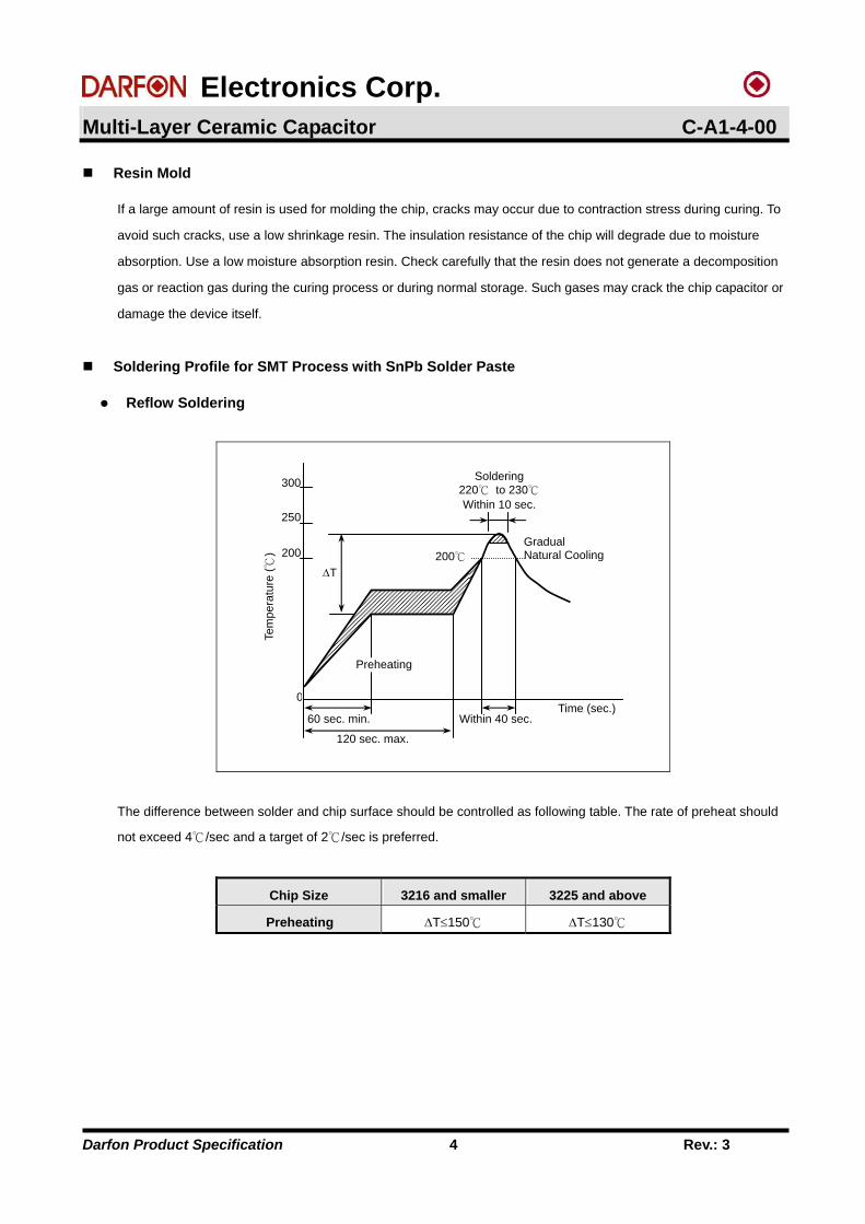
Soldering Profile for SMT Process with SnPb Solder Paste
Reflow Soldering
The difference between solder and chip surface should be controlled as following table. The rate of preheat should
not exceed 4/sec and a target of 2/sec is preferred.
Chip Size 3216 and smaller 3225 and above
Preheating T150 T130
0
300
250
200 200
Within 40 sec.
T
60 sec. min.
120 sec. max.
Soldering 220 to 230Within 10 sec.
Tem
pera
ture
(
)
Preheating
Time (sec.)
Gradual Natural Cooling
Electronics Corp.
Multi-Layer Ceramic Capacitor C-A1-4-00
Darfon Product Specification 5 Rev.: 3
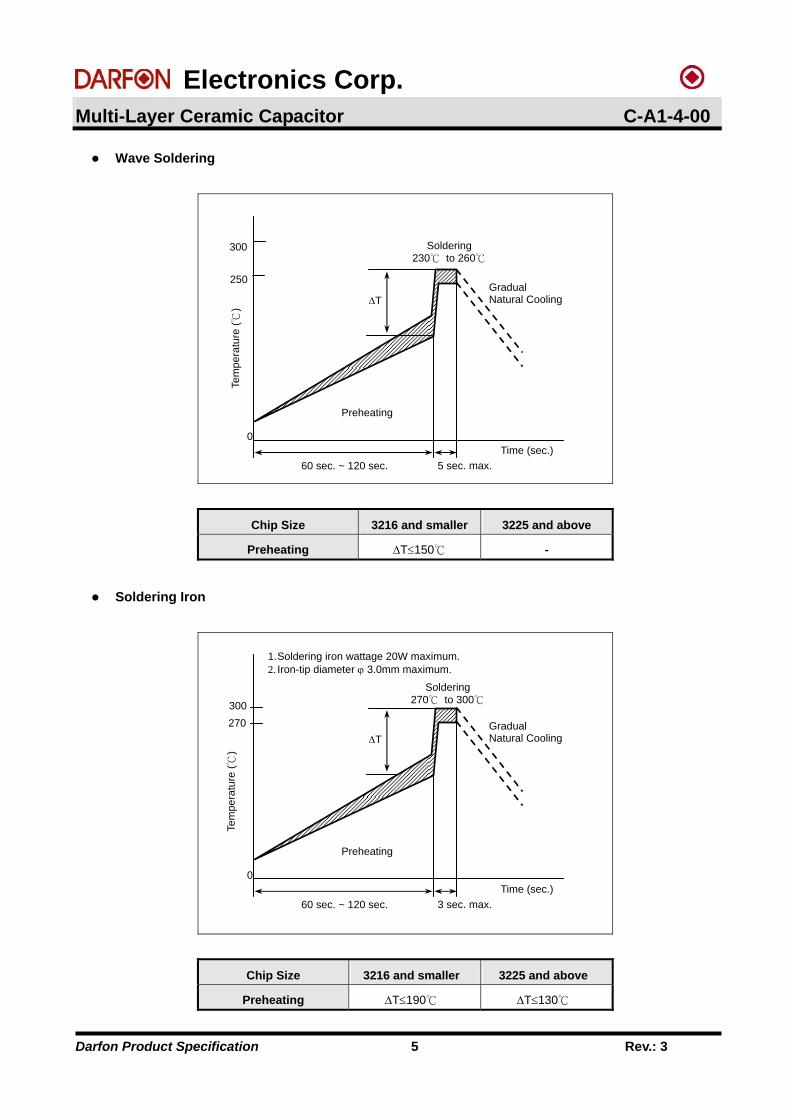
Wave Soldering
Chip Size 3216 and smaller 3225 and above
Preheating T150 -
Soldering Iron
Chip Size 3216 and smaller 3225 and above
Preheating T190 T130
0
300
250
5 sec. max.
T
Preheating
Time (sec.)
Gradual Natural Cooling
60 sec. ~ 120 sec.
Soldering 230 to 260
Tem
pera
ture
(
)
0
300
270
3 sec. max.
T
Preheating
Time (sec.)
Gradual Natural Cooling
60 sec. ~ 120 sec.
Soldering 270 to 300
Tem
pera
ture
(
)
1. Soldering iron wattage 20W maximum.2. Iron-tip diameter 3.0mm maximum.

Electronics Corp.
Multi-Layer Ceramic Capacitor C-A1-4-00
Darfon Product Specification 6 Rev.: 3
Soldering
Reflow Soldering for Lead free Termination
The difference between solder and chip surface should be controlled as following table. The rate of preheat should
not exceed 4/sec and a target of 2/sec is preferred.
Chip Size 3216 and smaller 3225 and above
Preheating T150 T130
Flow Soldering for Lead free Termination
Chip Size 3216 and smaller 3225 and above
Preheating T150 -
0
200
Over 200Within 90 sec.
T
60 sec. min.
120 sec. max.
Soldering 240 to 260Within 10 sec.
Tem
pera
ture
(
)
Preheating
Time (sec.)
Gradual Natural Cooling
300
250
Preheating
0
3 ~ 5 sec.
T
Time (sec.)
Gradual Natural Cooling
60 sec. ~ 120 sec.
Soldering 240 to 260
Tem
pera
ture
(
)
300
250
200

Electronics Corp.
Multi-Layer Ceramic Capacitor C-A1-4-00
Darfon Product Specification 7 Rev.: 3
Soldering Iron
Chip Size 3216 and smaller 3225 and above
Preheating T190 T130
0
300
270
3 sec. max.
T
Preheating
Time (sec.)
Gradual Natural Cooling
60 sec. ~ 120 sec.
Soldering 270 to 300
Tem
pera
ture
(
)1. Soldering iron wattage 20W maximum. 2. Iron-tip diameter 3.0mm maximum.

Electronics Corp.
Multi-Layer Ceramic Capacitor C-A1-4-00
Darfon Product Specification 8 Rev.: 3
Chip Layout and Breaking PCB
1. To layout the SMD capacitors for reducing bend stress from board deflection of PCB. The following are
examples of good and bad layout.
Recommended Not Recommended
2. When breaking PCB, the layout should be noted that the mechanical stresses are depending on the position of
capacitors. The following example shows recommendation for better design.
A
D
E
C
B
Perforation
Slit
Magnitude of stresses A > B = C > D > E

Electronics Corp.
Multi-Layer Ceramic Capacitor C-A1-4-00
Darfon Product Specification 9 Rev.: 3
Aging
The capacitance and dissipation factor of class 2 capacitors decreases with time. It is known as ‘aging’ that follows a
logarithmic low and expressed in terms of an aging constant. Aging is caused by a gradual re-alignment of the
crystalline structure of the ceramic. The aging constant is defined as the percentage loss of capacitance at a ‘time
decade’. The law of capacitance aging is expressed as following equation:
Ct2 = Ct1 x (1 – k x log10(t2/t1))
Ct1: Capacitance after t1 hours of start aging.
Ct2: Capacitance after t2 hours of start aging.
k: aging constant (capacitance decrease per decade)
t1, t2: time in hours from start of aging.
A typical curve of aging rate is shown in following figure.
-30.0
-25.0
-20.0
-15.0
-10.0
-5.0
0.0
5.0
10.0
1 10 100 1000 10000 100000
Typical Curve of Aging Rate of Different Dielectric Material
Cap
acita
nce
Cha
nge
Per
cent
(%
)
Time (Hours)
NP0
X7R, X5R
Y5V
When heating the capacitors above Curie temperature (130~150) the capacitance can be re-new. So
capacitance of class 2 capacitors will be complete de-aged by soldering process; subsequently a new aging process
begins.
Because of aging, it is specified an age for measurement to meet the prescribed tolerance for class 2 capacitors.
Normally, 1000 hours (t2=1000 hrs) is defined.


