

Nanotechnology Innovation SummitDecember 8-10, 2010
Facing Our Energy Challenges in a New Era of (Nano) Science
Dr. Patricia M. DehmerDeputy Director for Science Programs
Office of Science, U.S. Department of Energyhttp://www.science.doe.gov/SC-2/Deputy_Director-speeches-presentations.htm
The National Nanotechnology Initiative: Why DOE?
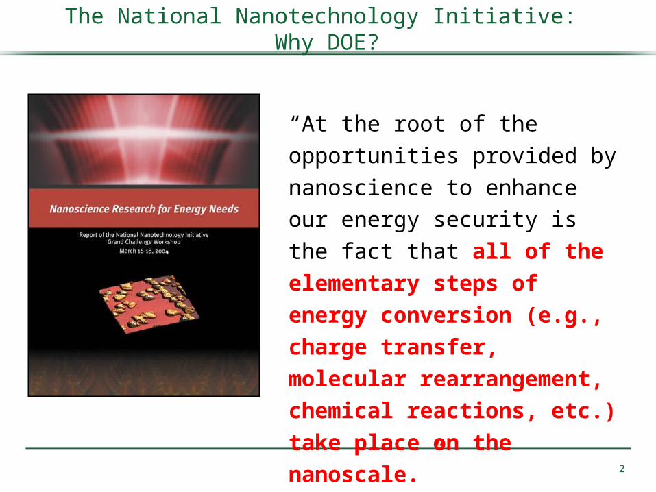
“At the root of the opportunities
provided by nanoscience to
enhance our energy security is
the fact that all of the elementary
steps of energy conversion
(e.g., charge transfer, molecular
rearrangement, chemical
reactions, etc.) take place on
the nanoscale.”
2

Defining the Role of DOE in the NNI
A workshop sponsored by the Office of Basic Energy Sciences in March 1999 defined the science agenda of the Office of Science in the NNI and provided the first recommendation for “infrastructure and facilities for nanoscale science and technology;” these facilities became one of the signature contributions of DOE to the NNI.
4

Nanoscale Science Research Centers (Artists’ Concepts, circa 2002)
Molecular Foundry(Lawrence Berkeley National Lab)
Center for Nanoscale Materials(Argonne National Lab)
Center for Functional Nanomaterials(Brookhaven National Lab)
Center for Integrated Nanotechnologies (Sandia & Los
Alamos National Labs)Center for Nanophase Materials Sciences
(Oak Ridge National Lab)
5
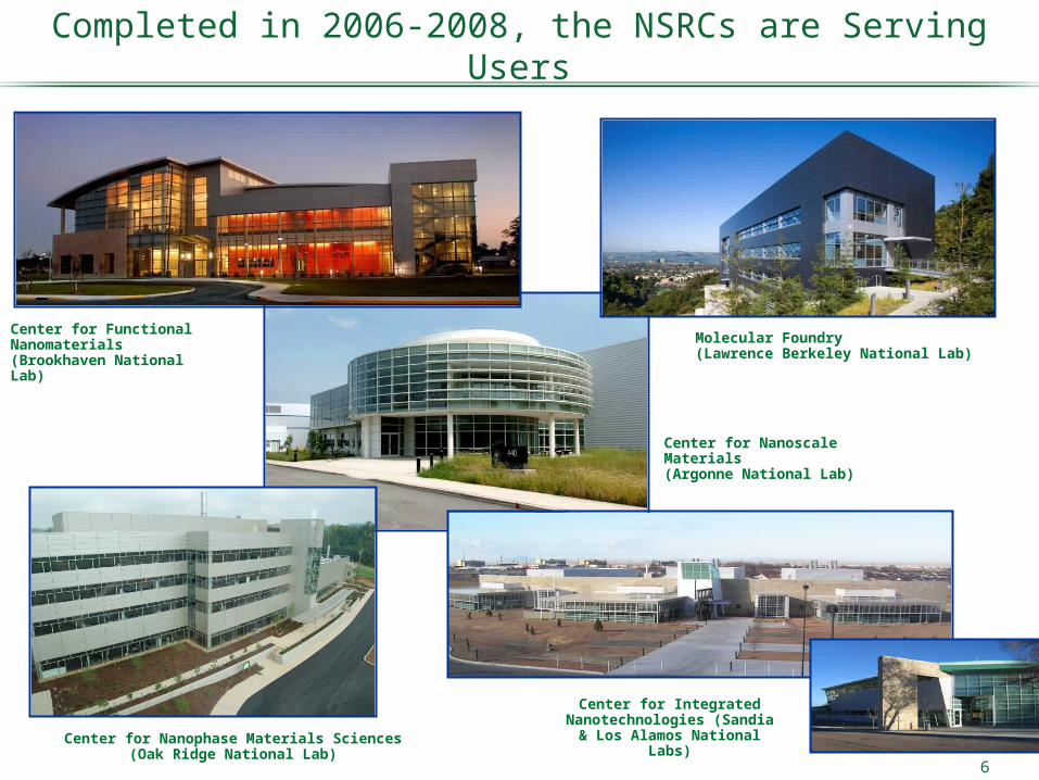
Completed in 2006-2008, the NSRCs are Serving Users
Molecular Foundry(Lawrence Berkeley National Lab)
Center for Functional Nanomaterials(Brookhaven National Lab)
Center for Integrated Nanotechnologies (Sandia & Los
Alamos National Labs)Center for Nanophase Materials Sciences(Oak Ridge National Lab)
Center for Nanoscale Materials(Argonne National Lab)
6
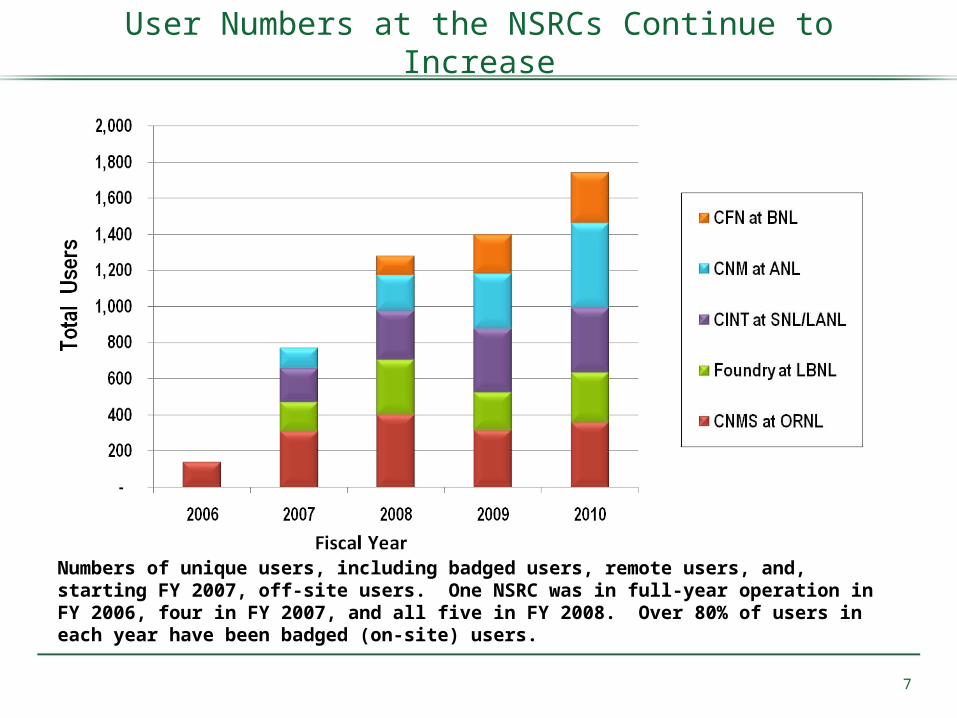
Numbers of unique users, including badged users, remote users, and, starting FY 2007, off-site users. One NSRC was in full-year operation in FY 2006, four in FY 2007, and all five in FY 2008. Over 80% of users in each year have been badged (on-site) users.
User Numbers at the NSRCs Continue to Increase
7

X-Ray Beamline with Nanoscale Resolution at the Advanced Photon Source
Unique instruments to study individual nanostructures
Quantitative structure, strain, orientation imaging
Sensitive trace element and chemical state analysis
“Discovery Platforms”: modular micro-labs for nanoscienceStandardized and batch fabricatedAccess to a range of diagnostic and characterization tools
Cantilever Array Discovery Platform: The size of an AFM chip, the CADP has multiple cantilevers projecteng from all edges for nanomechanics, novel scanning probe technologies, chem and bio sensing, magnetization studies, and studies of the physics of coupled systems.
NSRCs Create New Tools and Capabilities – Big and Small
8
Nano Tutorial on Energy:Nano Tutorial on Energy:Energy sources and consumption sectors in the U.S.
11

DomesticProduction:73 Quads
Imports:30 Quads
Consumption:95 Quads
Exports:7 Quads
En
erg
y S
up
ply
(Q
uad
s)
En
erg
y C
on
sum
pti
on
U.S. Energy Flow, 2009About 1/3 of U.S. primary energy is imported
12
Adjustments: 1 Quad
U.S. Share of World, 2007
Population EnergyProduction
EnergyConsumption
4.6%
15.0%
21.0%
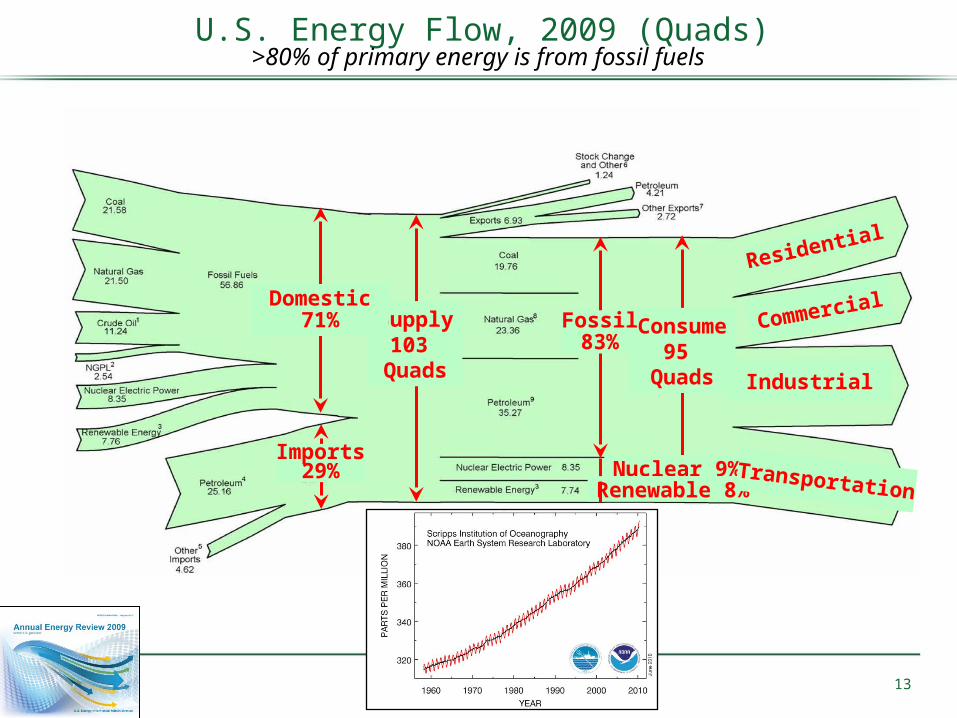
U.S. Energy Flow, 2009 (Quads)>80% of primary energy is from fossil fuels
Supply103
Quads
Domestic71%
Imports29%
Residential
Commercial
Industrial
Consume95
Quads
Nuclear 9%Renewable 8%
Fossil83%
Transportation
13

Source: Lawrence Livermore National Laboratory and the Department of Energy, Energy Information Administration, 2009 (based on data from DOE/EIA-0384(2008), June 2009).
U.S. Energy Production and Usage in 2008Units in Quadrillion BTUs (Quads)
14
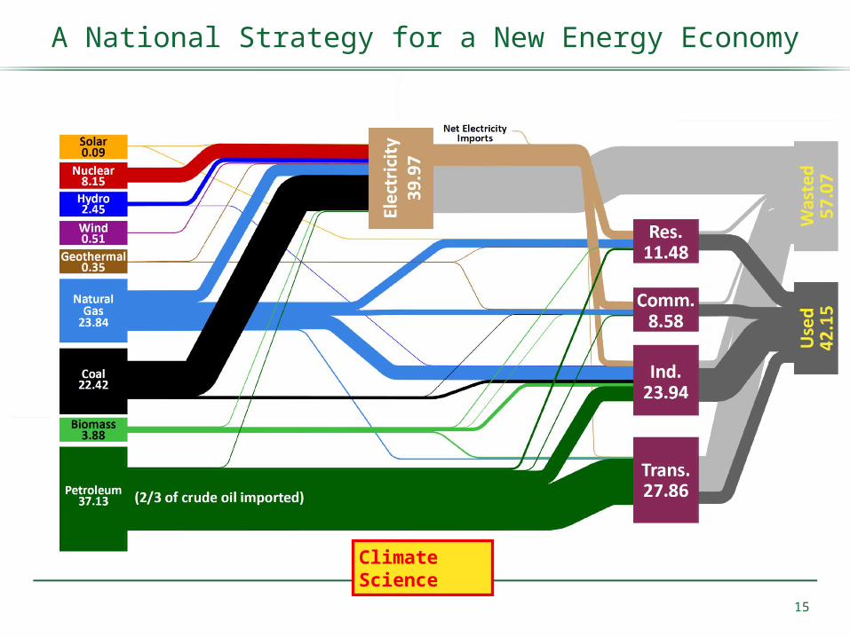
A National Strategy for a New Energy Economy
Climate Science
15

17
A Nano Research Agenda for a New Energy EconomyHigh-Tc and high current superconductors for grid and other electrical applications
Nanostructured thin-film organic photovoltaic devices
ArtificialPhotosynthesis
Structure of lignocellulose at the nanoscale and the rules by which plants create this material
Materials for energy efficient selective capture or separation of CO2 from gas mixtures
Conversion of electricity to light using new designs, such as luminescent nanowires, quantum dots, and hybrid architectures; energy conversion processes in structures whose sizes are even smaller than the wavelength of light; understand and eliminate defects in SSL semiconductor materials that presently limit the energy efficiency.

Take the “Beat-the-Leaf” Challenge
END


