Near and Long Term Challenges and Solutions for Low Power
Energy Scavenging Applications
Rajeevan AmirtharajahUniversity of California, Davis
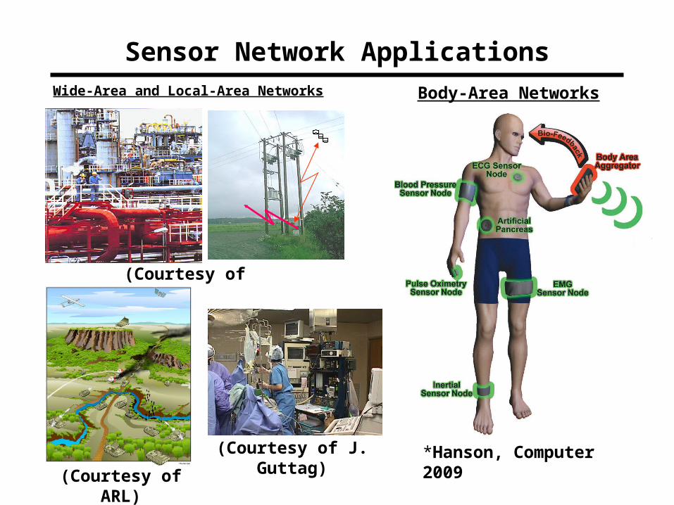
Sensor Network Applications
(Courtesy of ABB)
*Hanson, Computer 2009
Wide-Area and Local-Area Networks
(Courtesy of ARL)
Body-Area Networks
(Courtesy of J. Guttag)
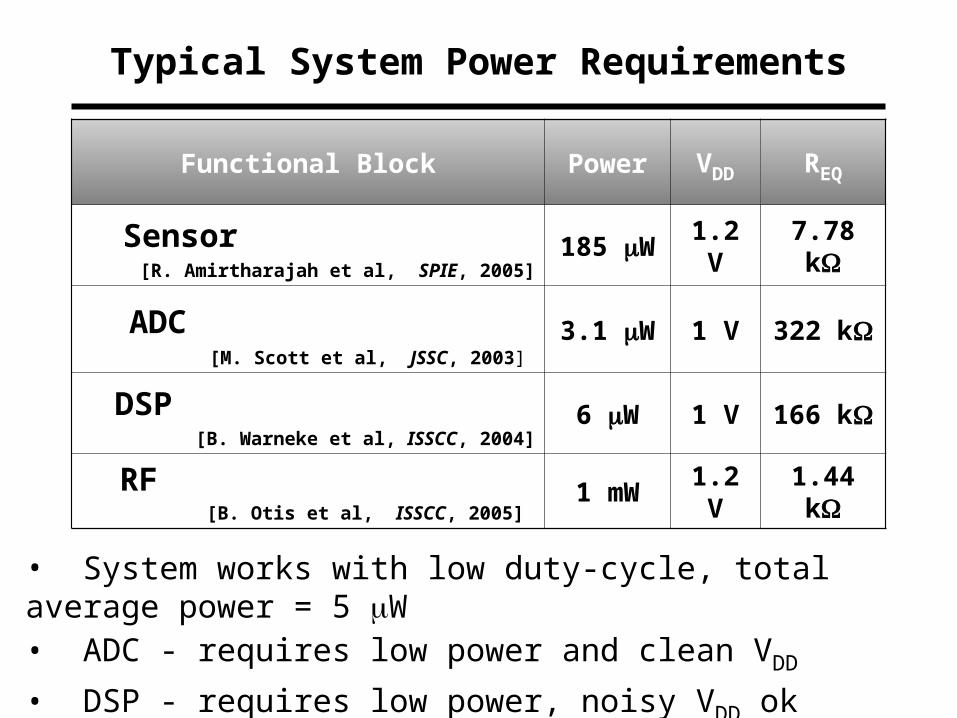
Typical System Power Requirements
• System works with low duty-cycle, total average power = 5 W• ADC - requires low power and clean VDD
• DSP - requires low power, noisy VDD ok• RF - requires high peak power
Functional Block Power VDD REQ
Sensor[R. Amirtharajah et al, SPIE, 2005]
185 W 1.2 V 7.78 k
ADC
[M. Scott et al, JSSC, 2003]
3.1 W 1 V 322 k
DSP[B. Warneke et al, ISSCC, 2004]
6 W 1 V 166 k
RF[B. Otis et al, ISSCC, 2005]
1 mW 1.2 V 1.44 k
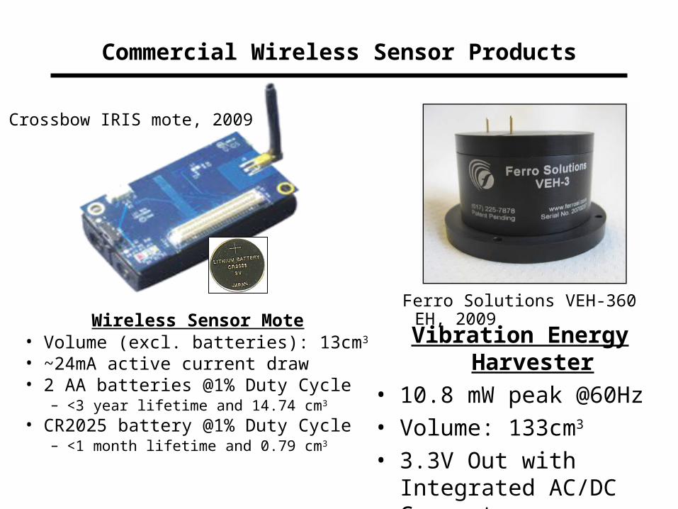
Commercial Wireless Sensor Products
Wireless Sensor Mote• Volume (excl. batteries): 13cm3
• ~24mA active current draw• 2 AA batteries @1% Duty Cycle
– <3 year lifetime and 14.74 cm3
• CR2025 battery @1% Duty Cycle– <1 month lifetime and 0.79 cm3
Crossbow IRIS mote, 2009
Ferro Solutions VEH-360 EH, 2009
Vibration Energy Harvester• 10.8 mW peak @60Hz• Volume: 133cm3
• 3.3V Out with Integrated AC/DC Converter
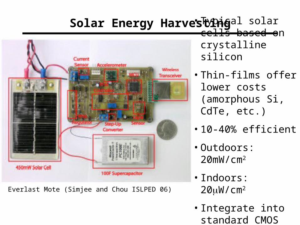
Solar Energy Harvesting
Everlast Mote (Simjee and Chou ISLPED 06)
• Typical solar cells based on crystalline silicon
• Thin-films offer lower costs (amorphous Si, CdTe, etc.)
• 10-40% efficient
• Outdoors: 20mW/cm2
• Indoors: 20W/cm2
• Integrate into standard CMOS
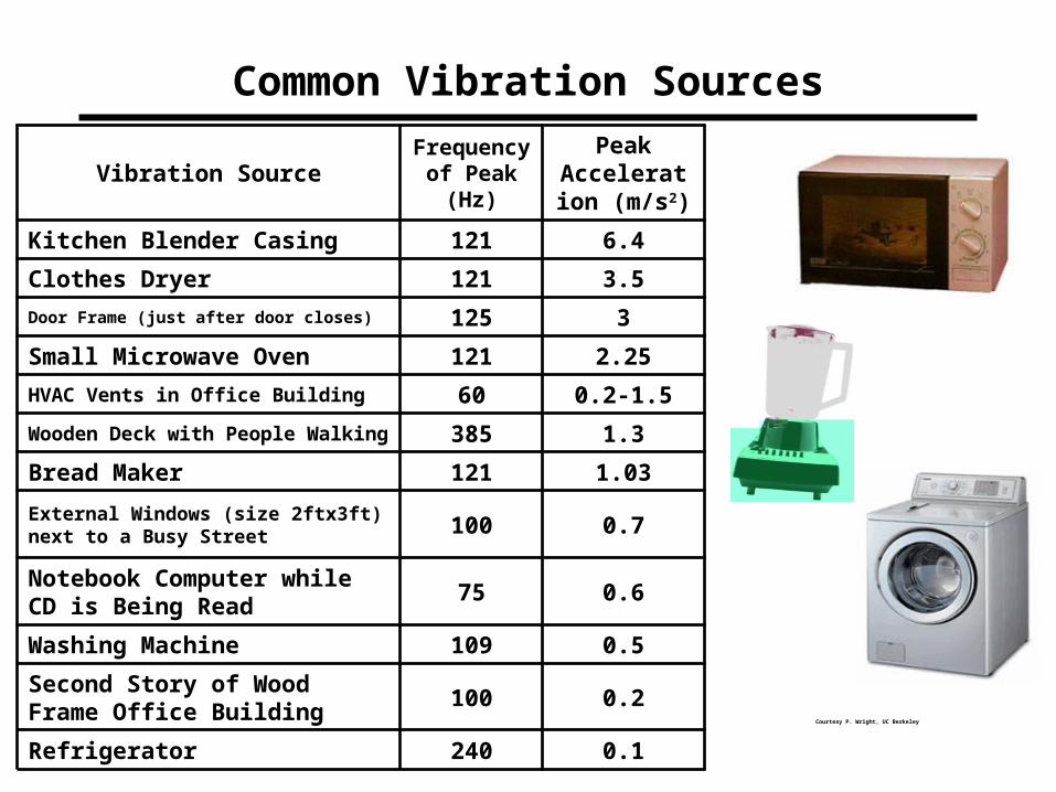
0.1240Refrigerator
0.2100Second Story of Wood Frame Office Building
0.5109Washing Machine
0.675Notebook Computer while CD is Being Read
0.7100External Windows (size 2ftx3ft) next to a Busy Street
1.03121Bread Maker
1.3385Wooden Deck with People Walking
0.2-1.560HVAC Vents in Office Building
2.25121Small Microwave Oven
3125Door Frame (just after door closes)
3.5121Clothes Dryer
6.4121Kitchen Blender Casing
Peak Acceleration
(m/s2)
Frequency of Peak
(Hz)Vibration Source
Courtesy P. Wright, UC Berkeley
Common Vibration Sources
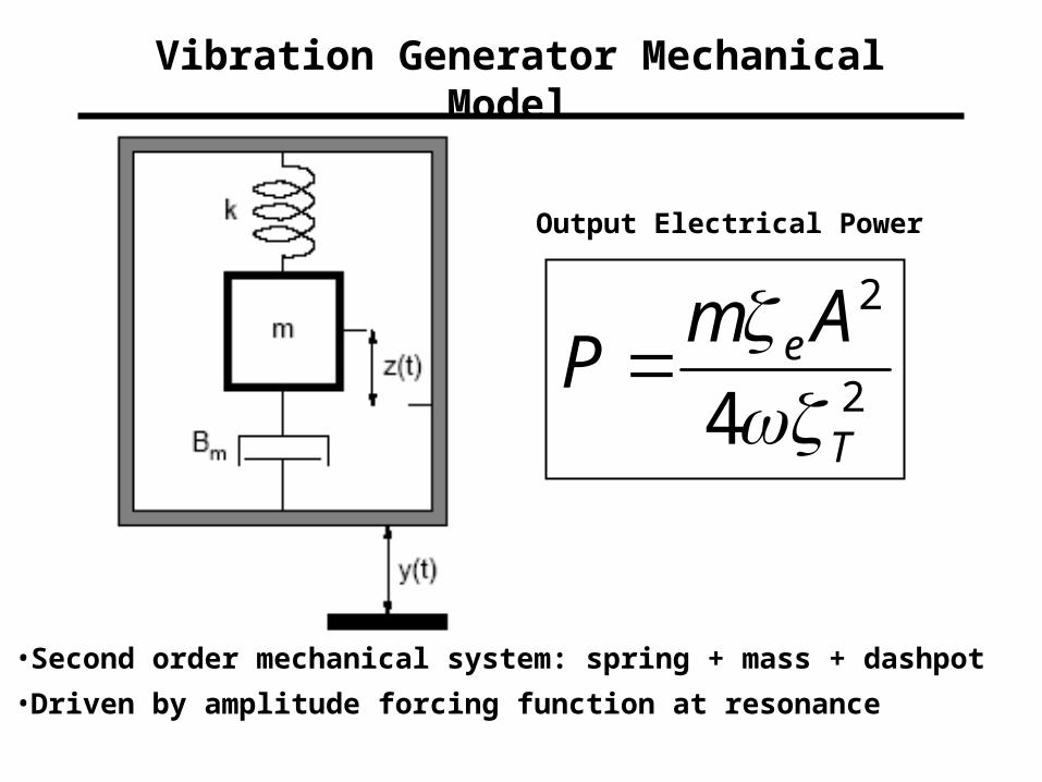
Vibration Generator Mechanical Model
• Second order mechanical system: spring + mass + dashpot
• Driven by amplitude forcing function at resonance
2
2
4 T
eAmP
Output Electrical Power
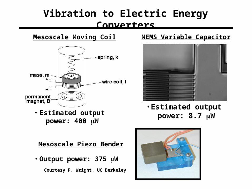
Vibration to Electric Energy Converters
Mesoscale Moving Coil MEMS Variable Capacitor
• Estimated output power: 400 W
• Estimated output power: 8.7 W
Mesoscale Piezo Bender
• Output power: 375 W
Courtesy P. Wright, UC Berkeley
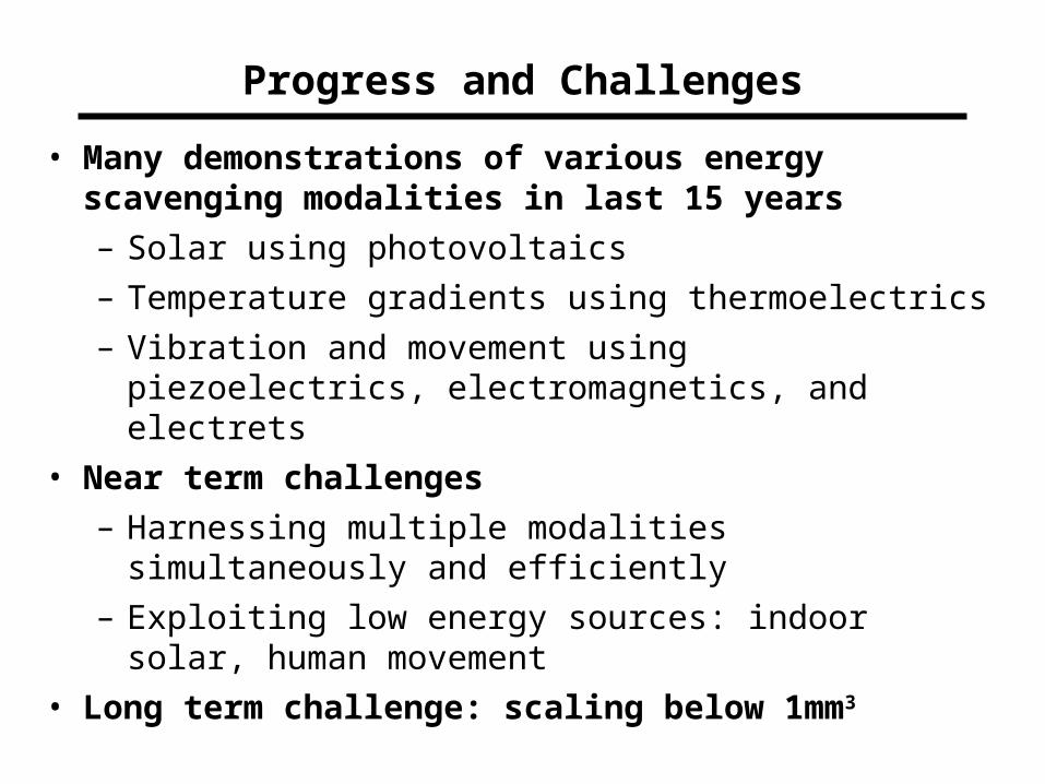
• Many demonstrations of various energy scavenging modalities in last 15 years
– Solar using photovoltaics
– Temperature gradients using thermoelectrics
– Vibration and movement using piezoelectrics, electromagnetics, and electrets
• Near term challenges
– Harnessing multiple modalities simultaneously and efficiently
– Exploiting low energy sources: indoor solar, human movement
• Long term challenge: scaling below 1mm3
Progress and Challenges
• Introduction
• Multiple Input Energy Harvesting
• System Miniaturization
• Conclusions
Outline
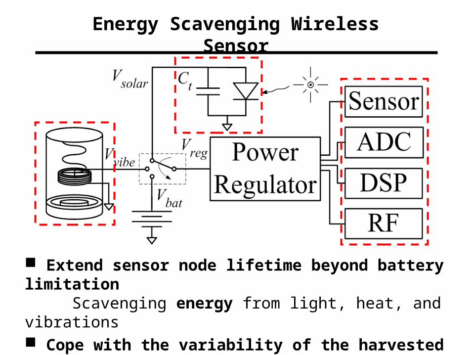
Energy Scavenging Wireless Sensor
Extend sensor node lifetime beyond battery limitation Scavenging energy from light, heat, and vibrations Cope with the variability of the harvested power
Energy scalable digital and mixed-signal processing
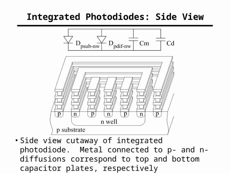
Integrated Photodiodes: Side View
• Side view cutaway of integrated photodiode. Metal connected to p- and n- diffusions correspond to top and bottom capacitor plates, respectively
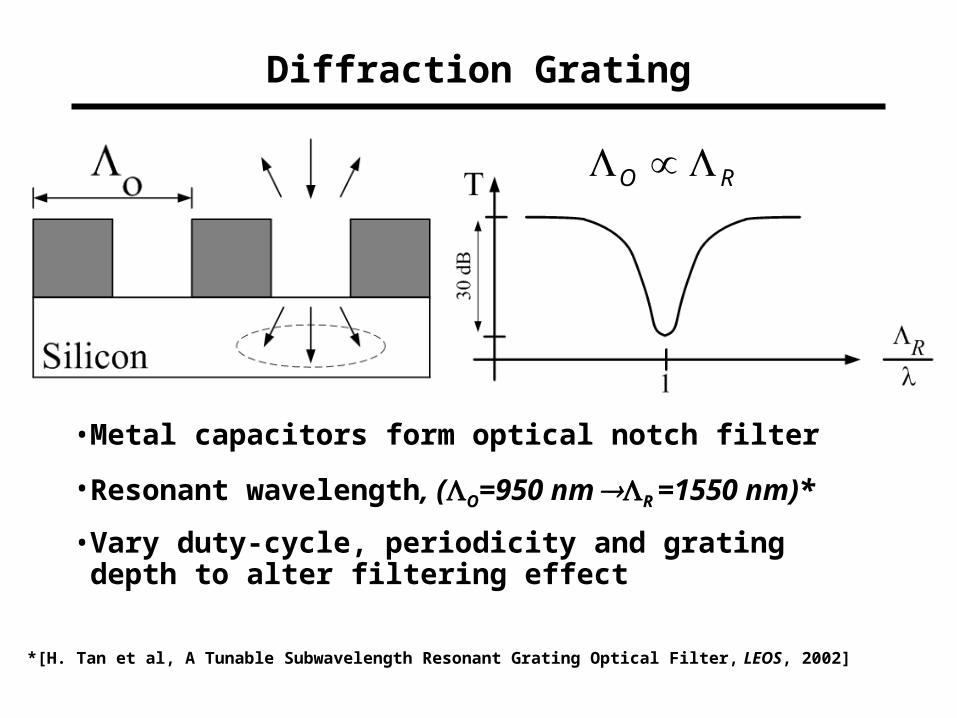
Diffraction Grating
• Metal capacitors form optical notch filter
• Resonant wavelength, (O=950 nm R =1550 nm)*
• Vary duty-cycle, periodicity and grating depth to alter filtering effect
RO
*[H. Tan et al, A Tunable Subwavelength Resonant Grating Optical Filter, LEOS, 2002]
P+
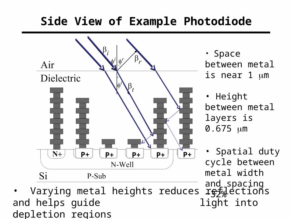
Side View of Example Photodiode
• Varying metal heights reduces reflections and helps guide l light into depletion regions
• Space between metal is near 1 m
• Height between metal layers is 0.675 m
• Spatial duty cycle between metal width and spacing ~32%
P+ P+P+ P+
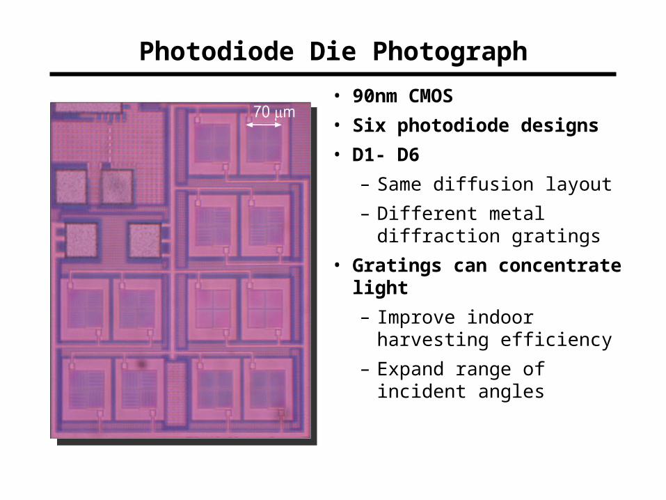
Photodiode Die Photograph
• 90nm CMOS
• Six photodiode designs
• D1- D6
– Same diffusion layout
– Different metal diffraction gratings
• Gratings can concentrate light
– Improve indoor harvesting efficiency
– Expand range of incident angles
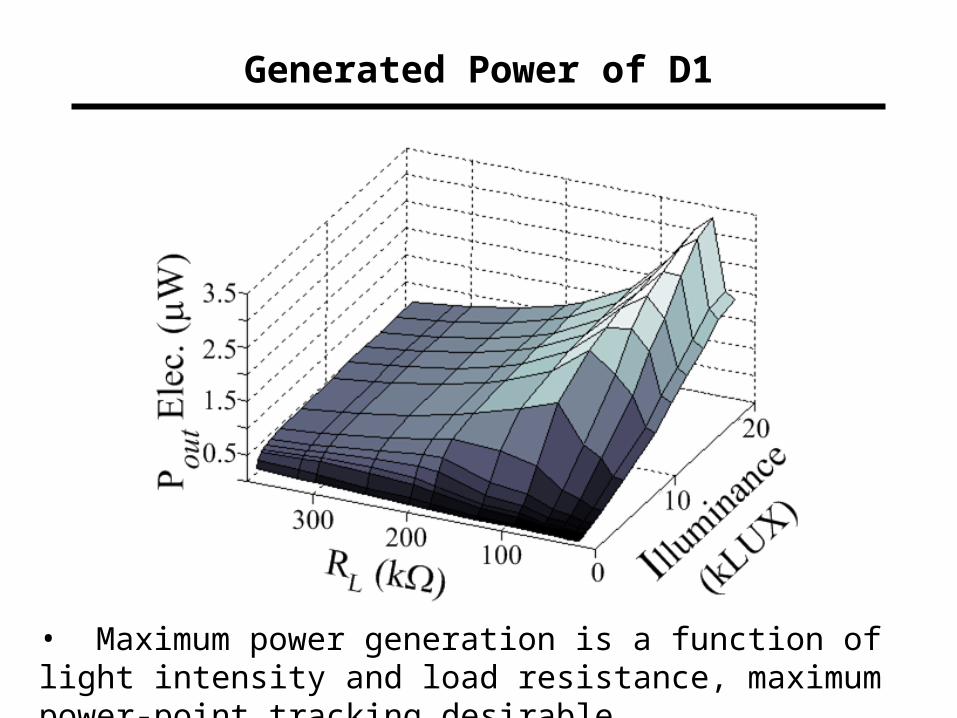
Generated Power of D1
• Maximum power generation is a function of light intensity and load resistance, maximum power-point tracking desirable
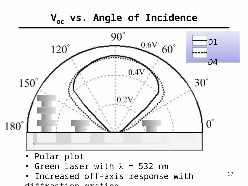
• Polar plot • Green laser with = 532 nm• Increased off-axis response with diffraction grating 17
Voc vs. Angle of Incidence
D1 D4 D1 D4
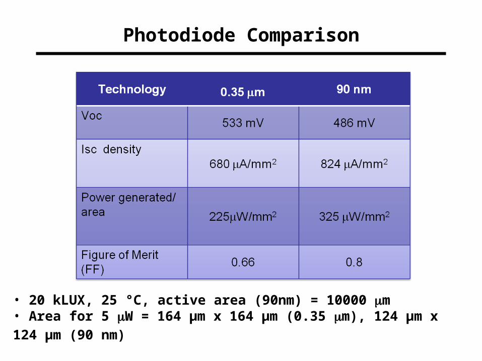
Photodiode Comparison
• 20 kLUX, 25 °C, active area (90nm) = 10000 m • Area for 5 W = 164 μm x 164 μm (0.35 m), 124 μm x 124 μm (90 nm)
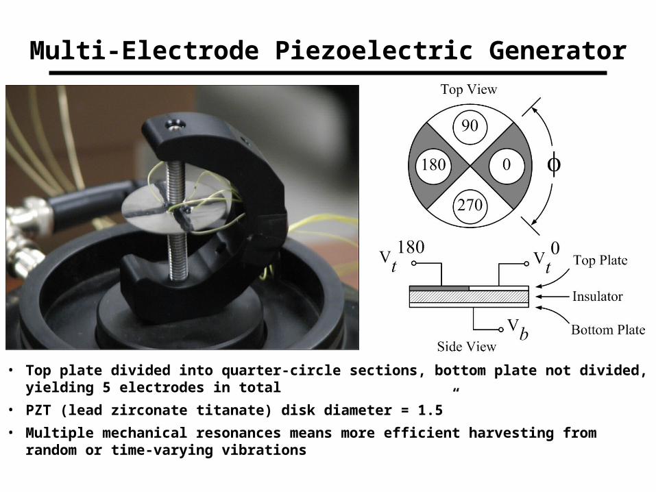
Multi-Electrode Piezoelectric Generator
• Top plate divided into quarter-circle sections, bottom plate not divided, yielding 5 electrodes in total
• PZT (lead zirconate titanate) disk diameter = 1.5”
• Multiple mechanical resonances means more efficient harvesting from random or time-varying vibrations
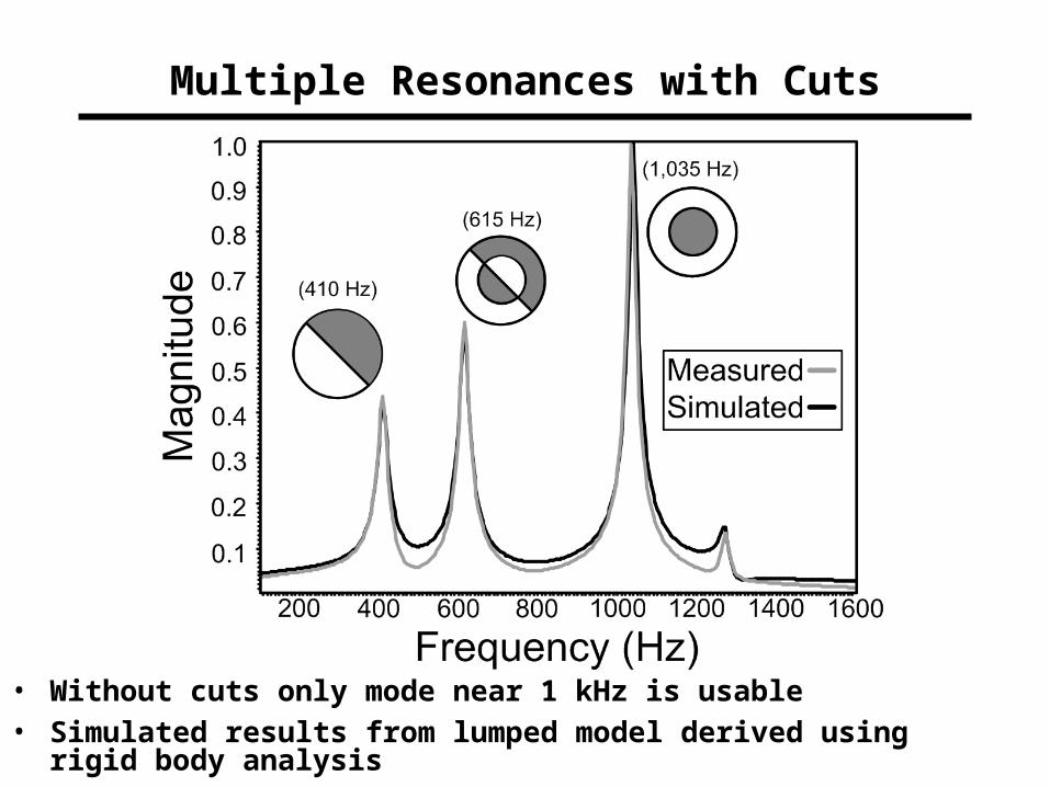
Multiple Resonances with Cuts
• Without cuts only mode near 1 kHz is usable• Simulated results from lumped model derived using rigid body
analysis
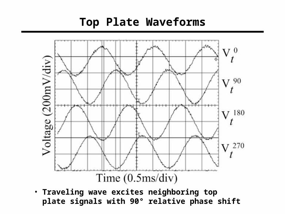
Top Plate Waveforms
• Traveling wave excites neighboring top plate signals with 90° relative phase shift
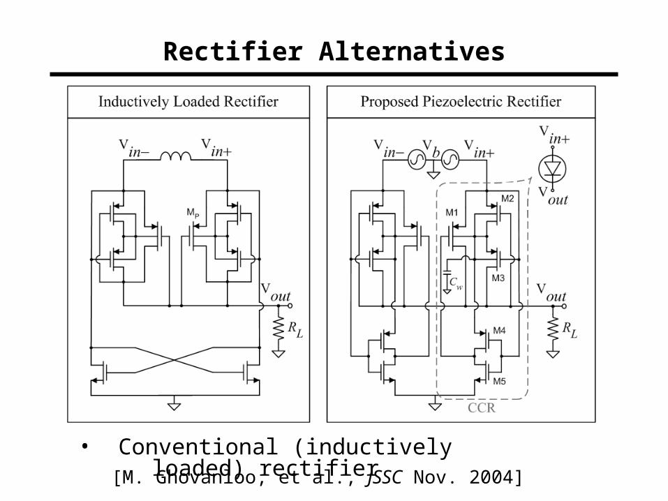
Rectifier Alternatives
• Conventional (inductively loaded) rectifier[M. Ghovanloo, et al., JSSC Nov. 2004]
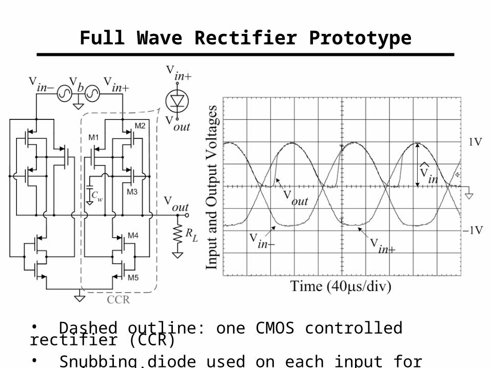
• Dashed outline: one CMOS controlled rectifier (CCR)• Snubbing diode used on each input for negative swings
Full Wave Rectifier Prototype
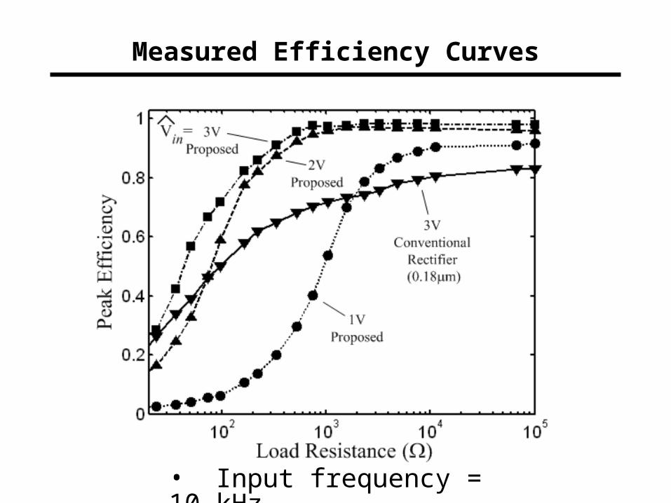
• Input frequency = 10 kHz
Measured Efficiency Curves
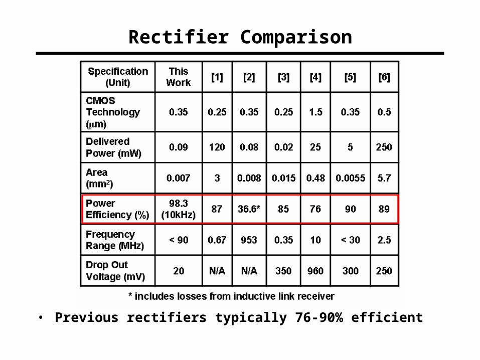
Rectifier Comparison
• Previous rectifiers typically 76-90% efficient
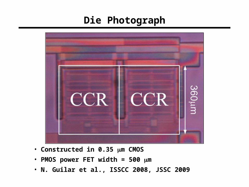
Die Photograph
• Constructed in 0.35 m CMOS
• PMOS power FET width = 500 m
• N. Guilar et al., ISSCC 2008, JSSC 2009
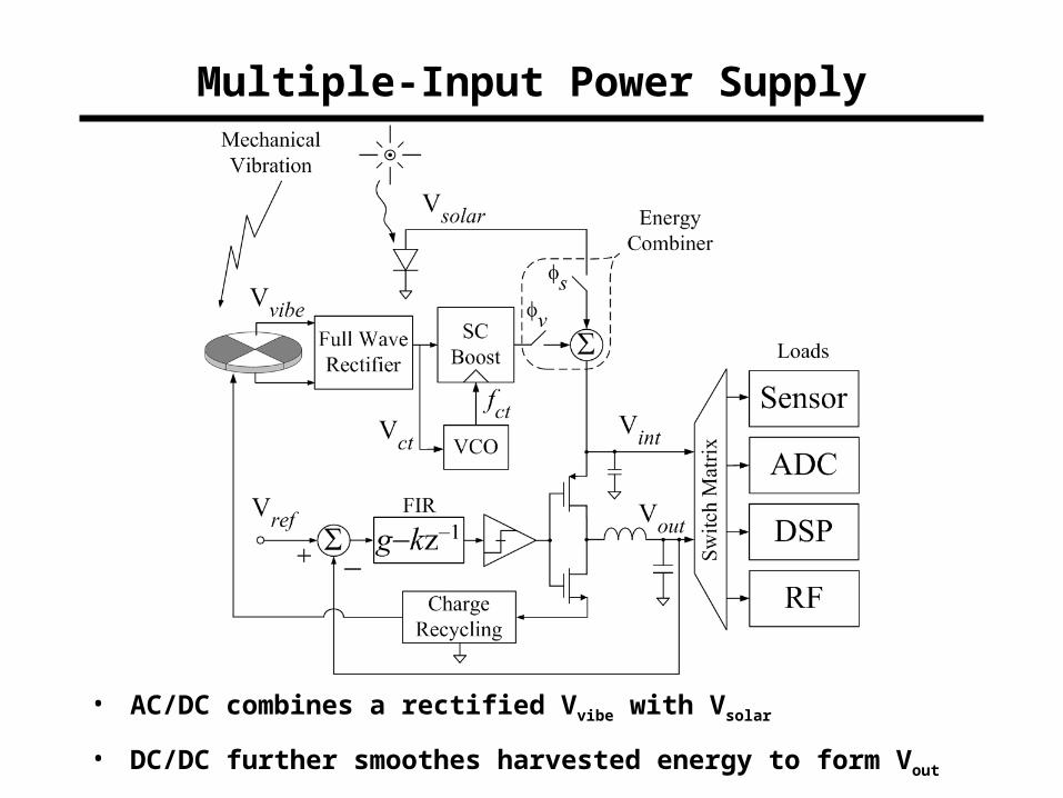
Multiple-Input Power Supply
• AC/DC combines a rectified Vvibe with Vsolar
• DC/DC further smoothes harvested energy to form Vout
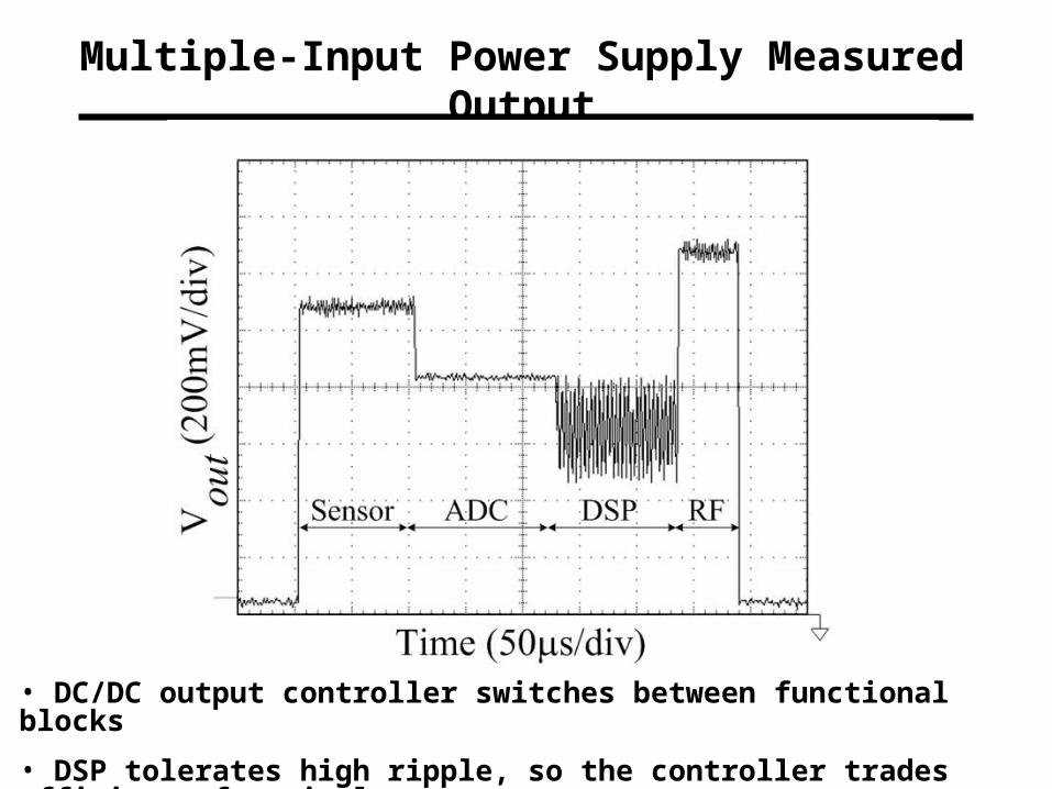
Multiple-Input Power Supply Measured Output
• DC/DC output controller switches between functional blocks
• DSP tolerates high ripple, so the controller trades efficiency for ripple
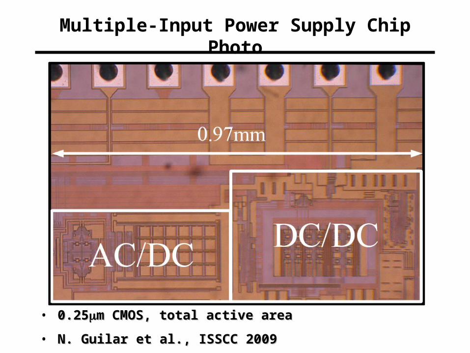
Multiple-Input Power Supply Chip Photo
• 0.250.25m CMOS, total active aream CMOS, total active area
• N. Guilar et al., ISSCC 2009N. Guilar et al., ISSCC 2009
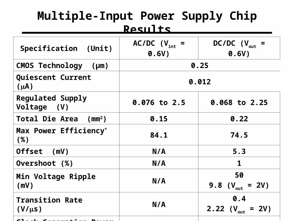
Multiple-Input Power Supply Chip Results
Specification (Unit) AC/DC (Vint = 0.6V) DC/DC (Vout = 0.6V)
CMOS Technology (μm) 0.25
Quiescent Current (A) 0.012
Regulated Supply Voltage (V) 0.076 to 2.5 0.068 to 2.25
Total Die Area (mm2) 0.15 0.22
Max Power Efficiency* (%) 84.1 74.5
Offset (mV) N/A 5.3
Overshoot (%) N/A 1
Min Voltage Ripple (mV) N/A50
9.8 (Vout = 2V)
Transition Rate (V/s) N/A0.4
2.22 (Vout = 2V)
Clock Generation Power (W) 4.5 13
Controller Power (W) 0.9 3
Delivered Power (W) 74 78
• Introduction
• Multiple Input Energy Harvesting
• System Miniaturization
• Conclusions
Outline
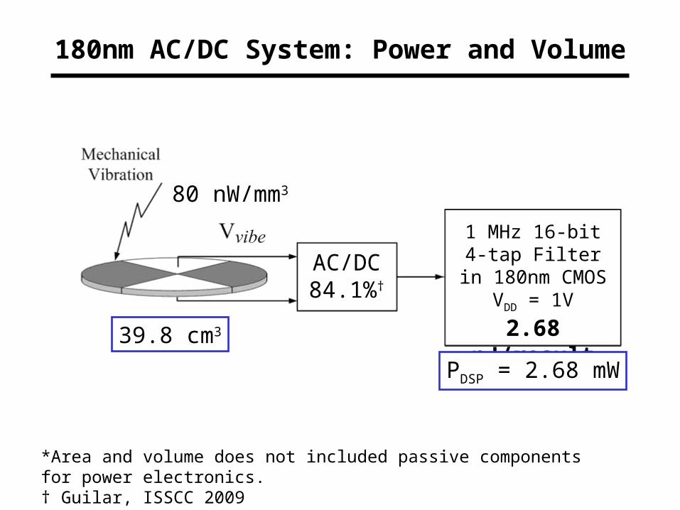
180nm AC/DC System: Power and Volume
1 MHz 16-bit4-tap Filter in
180nm CMOS VDD = 1V
2.68 nJ/result
AC/DC84.1%†
39.8 cm3
PDSP = 2.68 mW
*Area and volume does not included passive components for power electronics.† Guilar, ISSCC 2009
80 nW/mm3
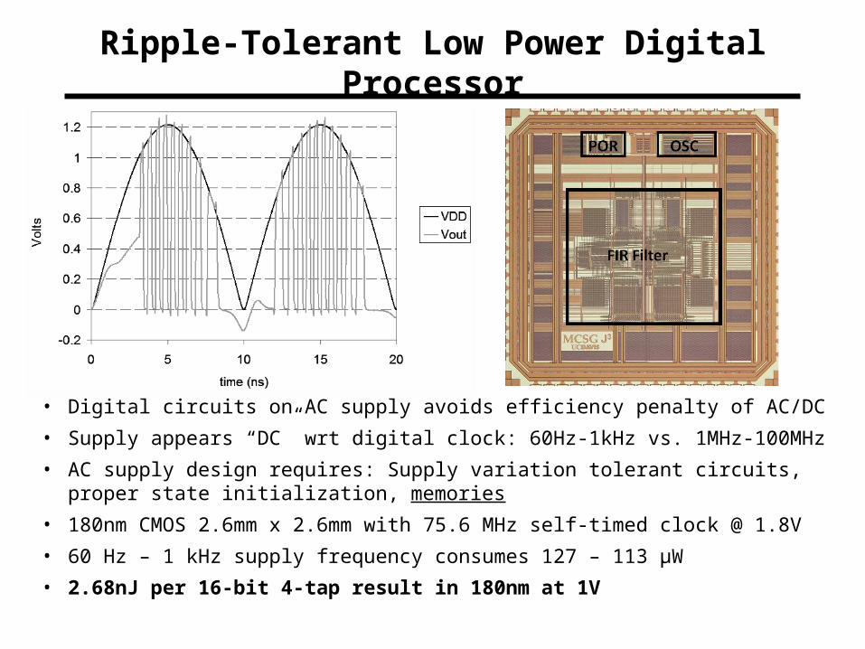
Ripple-Tolerant Low Power Digital Processor
• Digital circuits on AC supply avoids efficiency penalty of AC/DC
• Supply appears “DC” wrt digital clock: 60Hz-1kHz vs. 1MHz-100MHz
• AC supply design requires: Supply variation tolerant circuits, proper state initialization, memories
• 180nm CMOS 2.6mm x 2.6mm with 75.6 MHz self-timed clock @ 1.8V
• 60 Hz – 1 kHz supply frequency consumes 127 – 113 µW
• 2.68nJ per 16-bit 4-tap result in 180nm at 1V
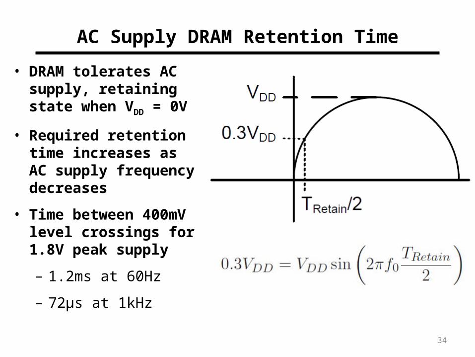
AC Supply DRAM Retention Time
• DRAM tolerates AC supply, retaining state when VDD = 0V
• Required retention time increases as AC supply frequency decreases
• Time between 400mV level crossings for 1.8V peak supply
– 1.2ms at 60Hz
– 72µs at 1kHz
34
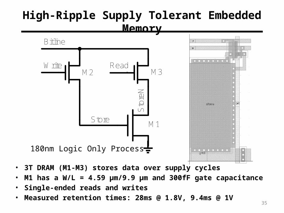
M3
M1
M2Write
Bitline
Read
Sto
reN
Store
High-Ripple Supply Tolerant Embedded Memory
• 3T DRAM (M1-M3) stores data over supply cycles• M1 has a W/L = 4.59 μm/9.9 μm and 300fF gate capacitance• Single-ended reads and writes• Measured retention times: 28ms @ 1.8V, 9.4ms @ 1V
180nm Logic Only Process
35
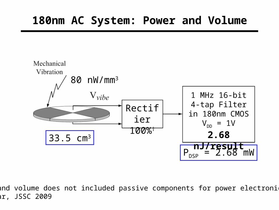
180nm AC System: Power and Volume
Rectifier100%†
33.5 cm3
PDSP = 2.68 mW
*Area and volume does not included passive components for power electronics.† Guilar, JSSC 2009
80 nW/mm3
1 MHz 16-bit4-tap Filter in
180nm CMOS VDD = 1V
2.68 nJ/result
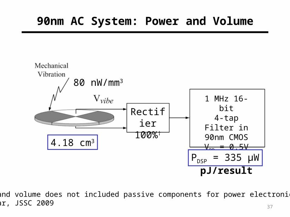
90nm AC System: Power and Volume
1 MHz 16-bit4-tap Filter in 90nm CMOSVDD = 0.5V
335 pJ/result
Rectifier100%†
4.18 cm3
PDSP = 335 µW
*Area and volume does not included passive components for power electronics.† Guilar, JSSC 2009
37
80 nW/mm3
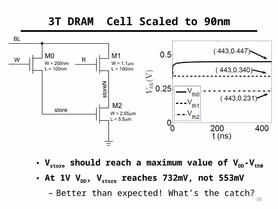
3T DRAM Cell Scaled to 90nm
• Vstore should reach a maximum value of VDD-Vth0
• At 1V VDD, Vstore reaches 732mV, not 553mV
– Better than expected! What’s the catch? 38
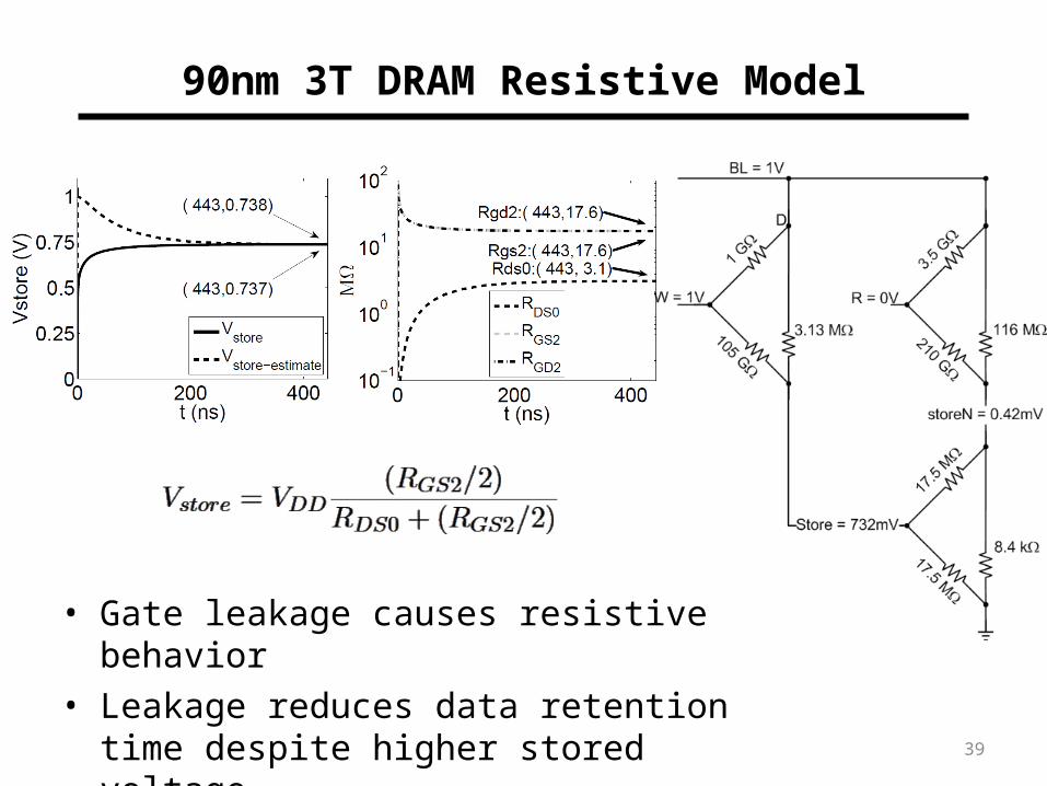
90nm 3T DRAM Resistive Model
39
• Gate leakage causes resistive behavior• Leakage reduces data retention time
despite higher stored voltage
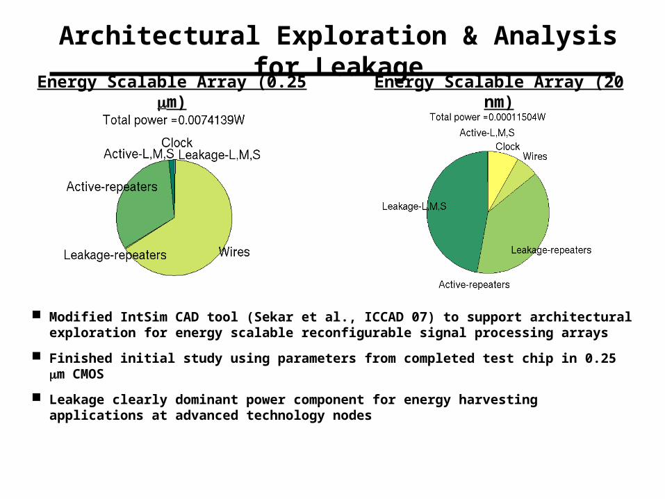
Architectural Exploration & Analysis for Leakage
Modified IntSim CAD tool (Sekar et al., ICCAD 07) to support architectural exploration for energy scalable reconfigurable signal processing arrays
Finished initial study using parameters from completed test chip in 0.25 m CMOS
Leakage clearly dominant power component for energy harvesting applications at advanced technology nodes
Energy Scalable Array (0.25 m) Energy Scalable Array (20 nm)
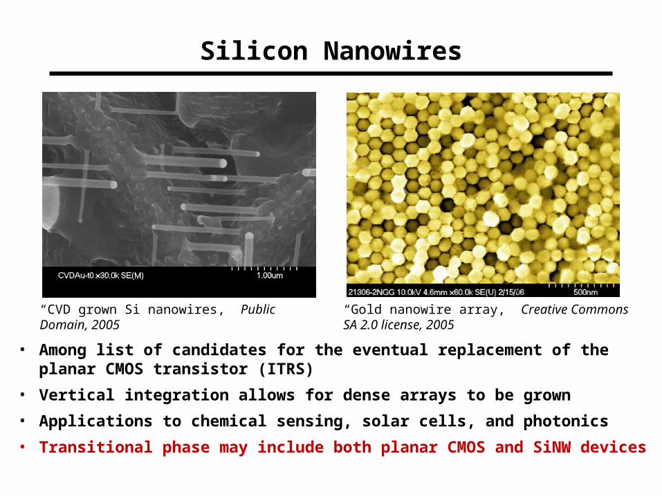
Silicon Nanowires
• Among list of candidates for the eventual replacement of the planar CMOS transistor (ITRS)
• Vertical integration allows for dense arrays to be grown
• Applications to chemical sensing, solar cells, and photonics
• Transitional phase may include both planar CMOS and SiNW devices
“Gold nanowire array,” Creative Commons SA 2.0 license, 2005
“CVD grown Si nanowires,” Public Domain, 2005
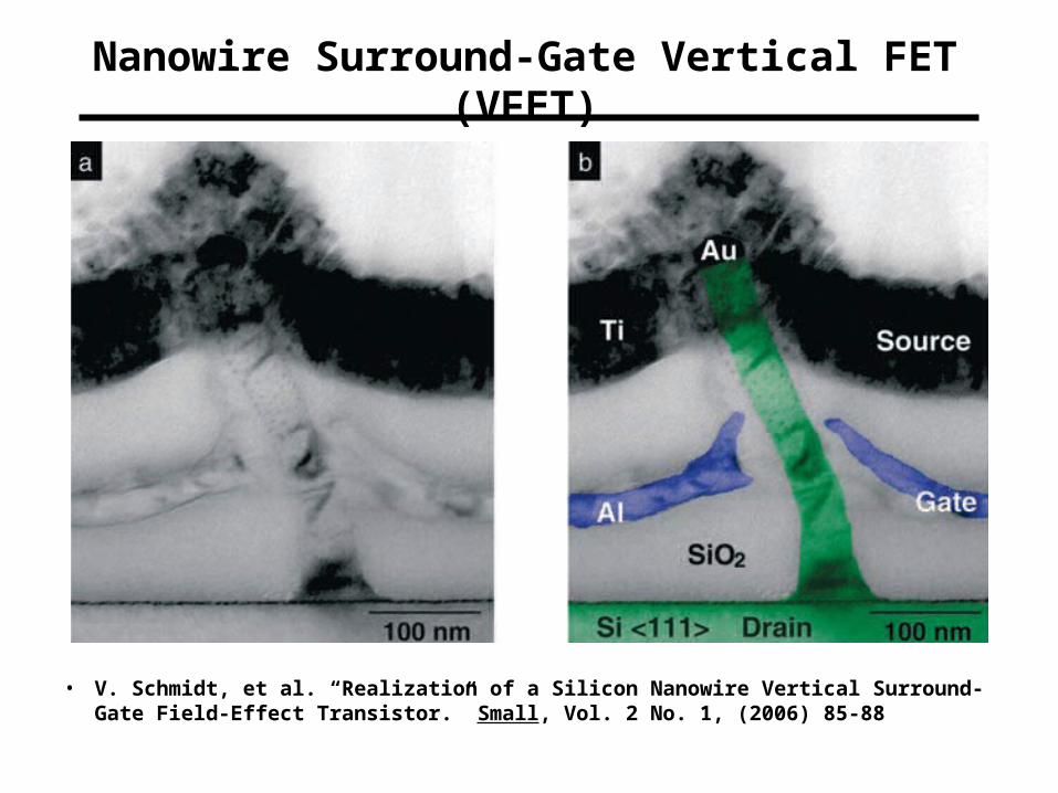
Nanowire Surround-Gate Vertical FET (VFET)
• V. Schmidt, et al. “Realization of a Silicon Nanowire Vertical Surround-Gate Field-Effect Transistor.” Small, Vol. 2 No. 1, (2006) 85-88
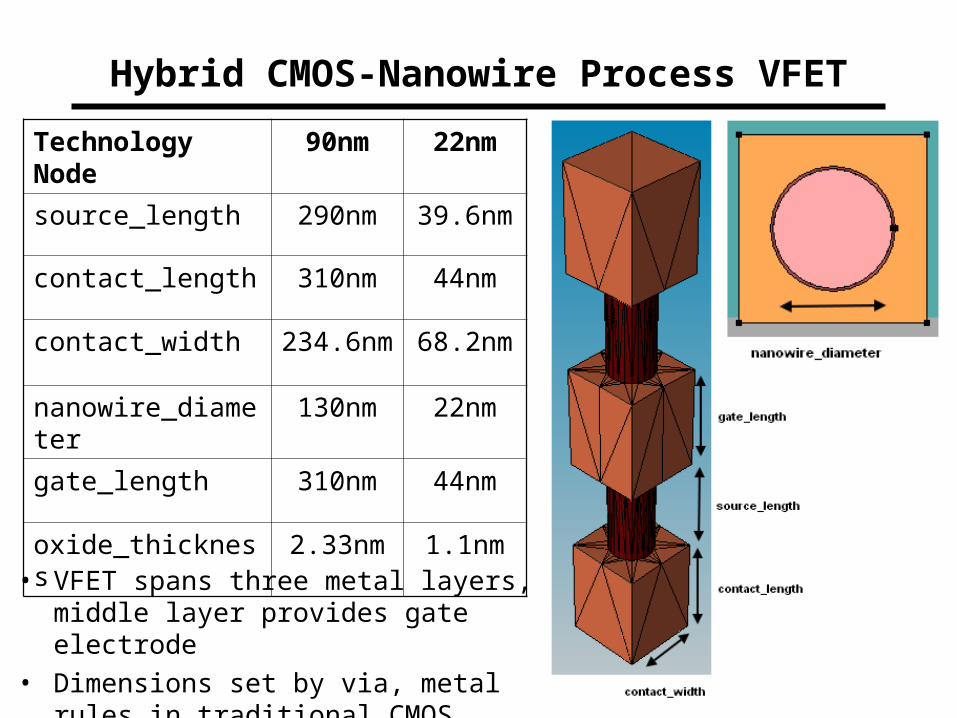
Hybrid CMOS-Nanowire Process VFET
Technology Node 90nm 22nm
source_length 290nm 39.6nm
contact_length 310nm 44nm
contact_width 234.6nm 68.2nm
nanowire_diameter 130nm 22nm
gate_length 310nm 44nm
oxide_thickness 2.33nm 1.1nm
• VFET spans three metal layers, middle layer provides gate electrode
• Dimensions set by via, metal rules in traditional CMOS process
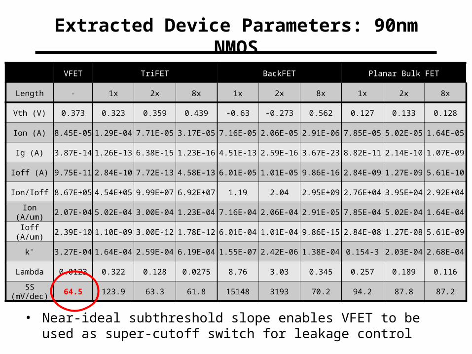
Extracted Device Parameters: 90nm NMOS
VFET TriFET BackFET Planar Bulk FET
Length - 1x 2x 8x 1x 2x 8x 1x 2x 8x
Vth (V) 0.373 0.323 0.359 0.439 -0.63 -0.273 0.562 0.127 0.133 0.128
Ion (A) 8.45E-05 1.29E-04 7.71E-05 3.17E-05 7.16E-05 2.06E-05 2.91E-06 7.85E-05 5.02E-05 1.64E-05
Ig (A) 3.87E-14 1.26E-13 6.38E-15 1.23E-16 4.51E-13 2.59E-16 3.67E-23 8.82E-11 2.14E-10 1.07E-09
Ioff (A) 9.75E-11 2.84E-10 7.72E-13 4.58E-13 6.01E-05 1.01E-05 9.86E-16 2.84E-09 1.27E-09 5.61E-10
Ion/Ioff 8.67E+05 4.54E+05 9.99E+07 6.92E+07 1.19 2.04 2.95E+09 2.76E+04 3.95E+04 2.92E+04
Ion (A/um) 2.07E-04 5.02E-04 3.00E-04 1.23E-04 7.16E-04 2.06E-04 2.91E-05 7.85E-04 5.02E-04 1.64E-04
Ioff (A/um) 2.39E-10 1.10E-09 3.00E-12 1.78E-12 6.01E-04 1.01E-04 9.86E-15 2.84E-08 1.27E-08 5.61E-09
k' 3.27E-04 1.64E-04 2.59E-04 6.19E-04 1.55E-07 2.42E-06 1.38E-04 0.154-3 2.03E-04 2.68E-04
Lambda 0.0123 0.322 0.128 0.0275 8.76 3.03 0.345 0.257 0.189 0.116
SS (mV/dec) 64.5 123.9 63.3 61.8 15148 3193 70.2 94.2 87.8 87.2
• Near-ideal subthreshold slope enables VFET to be used as super-cutoff switch for leakage control
• Introduction
• Multiple Input Energy Harvesting
• System Miniaturization
• Conclusions
Outline
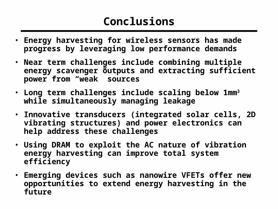
Conclusions
• Energy harvesting for wireless sensors has made progress by leveraging low performance demands
• Near term challenges include combining multiple energy scavenger outputs and extracting sufficient power from “weak” sources
• Long term challenges include scaling below 1mm3 while simultaneously managing leakage
• Innovative transducers (integrated solar cells, 2D vibrating structures) and power electronics can help address these challenges
• Using DRAM to exploit the AC nature of vibration energy harvesting can improve total system efficiency
• Emerging devices such as nanowire VFETs offer new opportunities to extend energy harvesting in the future
Acknowledgments
• Albert Chen
• Jamie Collier
• Erin Fong
• Liping Guo
• Nate Guilar
• Travis Kleeburg
• Prof. Stephen Lewis, UCD
• Jeff Loo
• Mackenzie Scott
• Jeff Siebert
• Justin Wenck
• Prof. Paul Wright, UCB
• Prof. Diego Yankelevich, UCD
• Prof. Paul Hurst, UCD

Acknowledgments
• National Science Foundation CAREER Award
• FCRP Interconnect Focus Center
• Xilinx University Program and Xilinx Research Labs
• U.S. Dept. of Education GAANN Fellowship
• The TSMC University Program