
NJG1170UX2
- 1 - Ver.2017-03-08
Low Noise Amplifier with Bypass for LTE
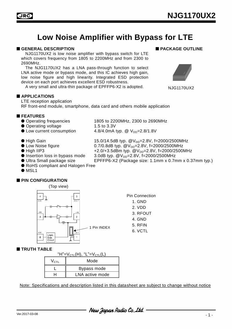
GENERAL DESCRIPTION PACKAGE OUTLINE NJG1170UX2 is low noise amplifier with bypass switch for LTE
which covers frequency from 1805 to 2200MHz and from 2300 to 2690MHz.
The NJG1170UX2 has a LNA pass-through function to select LNA active mode or bypass mode, and this IC achieves high gain, low noise figure and high linearity. Integrated ESD protection device on each port achieves excellent ESD robustness.
A very small and ultra-thin package of EPFFP6-X2 is adopted.
APPLICATIONS LTE reception application
RF front-end module, smartphone, data card and others mobile application FEATURES Operating frequencies 1805 to 2200MHz, 2300 to 2690MHz Operating voltage 1.5 to 3.3V Low current consumption 4.8/4.0mA typ. @ VDD=2.8/1.8V High Gain 15.0/14.5dB typ. @VDD=2.8V, f=2000/2500MHz Low Noise figure 0.7/0.8dB typ. @VDD=2.8V, f=2000/2500MHz High IIP3 +2.0/+3.5dBm typ. @VDD=2.8V, f=2000/2500MHz Insertion loss in bypass mode 3.0dB typ. @VDD=2.8V, f=2000/2500MHz Ultra Small package size EPFFP6-X2 (Package size: 1.1mm x 0.7mm x 0.37mm typ.) RoHS compliant and Halogen Free MSL1
PIN CONFIGURATION
TRUTH TABLE
“H”=VCTL(H), “L”=VCTL(L)
Note: Specifications and description listed in this datasheet are subject to change without notice
VCTL Mode
L Bypass mode
H LNA active mode
(Top view)
Pin Connection
1. GND
2. VDD
3. RFOUT
4. GND
5. RFIN
6. VCTL 1 Pin INDEX
NJG1170UX2

NJG1170UX2
- 2 -
ABSOLUTE MAXIMUM RATINGS
General condition: Ta=+25°C, Zs=Zl=50
PARAMETER SYMBOL CONDITIONS RATINGS UNITS
Supply voltage VDD 5.0 V
Control voltage VCTL 5.0 V
Input power PIN VDD=2.8V +15 dBm
Power dissipation PD 4-layer FR4 PCB with through-hole (101.5x114.5mm), Tj=150°C
430 mW
Operating temperature Topr -40 to +105 °C
Storage temperature Tstg -55 to +150 °C
ELECTRICAL CHARACTERISTICS 1 (DC CHARACTERISTICS)
General condition: Ta=+25°C, Zs=Zl=50
PARAMETERS SYMBOL CONDITIONS MIN TYP MAX UNITS
Operating voltage VDD 1.5 - 3.3 V
Control voltage (High) VCTL(H) 1.3 1.8 3.3 V
Control voltage (Low) VCTL(L) 0 0 0.3 V
Operating current 1 IDD 1 RF OFF, VDD=2.8V VCTL=1.8V
- 4.8 8.0 mA
Operating current 2 IDD 2 RF OFF, VDD=1.8V VCTL=1.8V
- 4.0 7.5 mA
Operating current 3 IDD 3 RF OFF, VDD=2.8V, VCTL=0V
- 15 60 A
Operating current 4 IDD 4 RF OFF, VDD=1.8V, VCTL=0V
- 10 60 A
Control current ICTL RF OFF, VCTL=1.8V - 7 20 A

NJG1170UX2
- 3 -
ELECTRICAL CHARACTERISTICS2 (LNA active mode)
General Condition: VDD=2.8V, VCTL=1.8V, fRF=2000MHz, Ta=+25°C, Zs=Zl=50, with application circuit
PARAMETERS SYMBOL CONDITIONS MIN TYP MAX UNITS
Small signal gain 1 Gain 1 Exclude PCB & connector losses(0.21dB)
11.5 15.0 16.5 dB
Noise figure 1 NF 1 Exclude PCB & connector losses(0.09dB)
- 0.7 1.1 dB
Input power at 1dB gain compression point 1(1)
P-1dB (IN) 1(1)
-13.0 -8.5 - dBm
Input 3rd order intercept point 1(1)
IIP3_1(1) f1=fRF, f2=fRF +1MHz, PIN=-30dBm
-3.0 +2.0 - dBm
Gain settling time1(1) Ts 1(1) Bypass to LNA active mode To be within 1dB of the final gain
- 1.0 2.5 µs
Gain settling time 1(2) Ts 1(2) LNA active to Bypass mode To be within 1dB of the final Insertion loss
- 1.0 2.5 µs
RF IN Return loss 1(1) RLi 1(1) 4.0 9.0 - dB
RF OUT Return loss1(1) RLo 1(1) 6.0 12.0 - dB
ELECTRICAL CHARACTERISTICS 3 (Bypass mode)
General Condition: VDD=2.8V, VCTL=0V, fRF=2000MHz, Ta=+25°C, Zs=Zl=50, with application circuit
PARAMETERS SYMBOL CONDITIONS MIN TYP MAX UNITS
Insertion Loss 1 LOSS 1 Exclude PCB & connector losses(0.21dB)
- 3.0 5.2 dB
Input power at 1dB gain compression point 1(2)
P-1dB (IN) 1(2)
0.0 +10.0 - dBm
Input 3rd order intercept point 1(2)
IIP3_1(2) f1=fRF, f2=fRF +1MHz, PIN=-10dBm
+2.0 +17.0 - dBm
RF IN Return loss 1(2) RLi 1(2) 4.0 7.0 - dB
RF OUT Return loss1(2) RLo 1(2) 3.0 5.0 - dB
NJG1170UX2
- 4 -
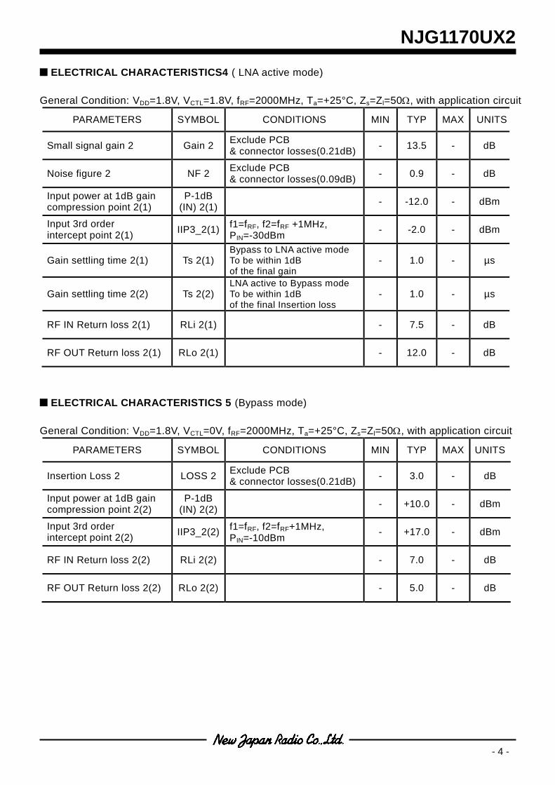
ELECTRICAL CHARACTERISTICS4 ( LNA active mode)
General Condition: VDD=1.8V, VCTL=1.8V, fRF=2000MHz, Ta=+25°C, Zs=Zl=50, with application circuit
PARAMETERS SYMBOL CONDITIONS MIN TYP MAX UNITS
Small signal gain 2 Gain 2 Exclude PCB & connector losses(0.21dB)
- 13.5 - dB
Noise figure 2 NF 2 Exclude PCB & connector losses(0.09dB)
- 0.9 - dB
Input power at 1dB gain compression point 2(1)
P-1dB (IN) 2(1)
- -12.0 - dBm
Input 3rd order intercept point 2(1)
IIP3_2(1) f1=fRF, f2=fRF +1MHz, PIN=-30dBm
- -2.0 - dBm
Gain settling time 2(1) Ts 2(1) Bypass to LNA active mode To be within 1dB of the final gain
- 1.0 - µs
Gain settling time 2(2) Ts 2(2) LNA active to Bypass mode To be within 1dB of the final Insertion loss
- 1.0 - µs
RF IN Return loss 2(1) RLi 2(1) - 7.5 - dB
RF OUT Return loss 2(1) RLo 2(1) - 12.0 - dB
ELECTRICAL CHARACTERISTICS 5 (Bypass mode)
General Condition: VDD=1.8V, VCTL=0V, fRF=2000MHz, Ta=+25°C, Zs=Zl=50, with application circuit
PARAMETERS SYMBOL CONDITIONS MIN TYP MAX UNITS
Insertion Loss 2 LOSS 2 Exclude PCB & connector losses(0.21dB)
- 3.0 - dB
Input power at 1dB gain compression point 2(2)
P-1dB (IN) 2(2)
- +10.0 - dBm
Input 3rd order intercept point 2(2)
IIP3_2(2) f1=fRF, f2=fRF+1MHz, PIN=-10dBm
- +17.0 - dBm
RF IN Return loss 2(2) RLi 2(2) - 7.0 - dB
RF OUT Return loss 2(2) RLo 2(2) - 5.0 - dB

NJG1170UX2
- 5 -
ELECTRICAL CHARACTERISTICS 6 ( LNA active mode)
General Condition: VDD=2.8V, VCTL=1.8V, fRF=2500MHz, Ta=+25°C, Zs=Zl=50, with application circuit
PARAMETERS SYMBOL CONDITIONS MIN TYP MAX UNITS
Small signal gain 3 Gain 3 Exclude PCB & connector losses(0.25dB)
11.5 14.5 16.0 dB
Noise figure 3 NF 3 Exclude PCB & connector losses(0.11dB)
- 0.8 1.2 dB
Input power at 1dB gain compression point 3(1)
P-1dB (IN) 3(1)
-12.0 -8.0 - dBm
Input 3rd order intercept point 3(1)
IIP3_3(1) f1=fRF, f2=fRF +1MHz, PIN=-30dBm
-2.0 +3.5 - dBm
Gain settling time 3(1) Ts 3(1) Bypass to LNA active mode To be within 1dB of the final gain
- 1.0 2.5 µs
Gain settling time 3(2) Ts 3(2) LNA active to Bypass mode To be within 1dB of the final Insertion loss
- 1.0 2.5 µs
RF IN Return loss 3(1) RLi 3(1) 6.0 12.0 - dB
RF OUT Return loss 3(1) RLo 3(1) 12.0 16.0 - dB
ELECTRICAL CHARACTERISTICS 7 (Bypass mode)
General Condition: VDD=2.8V, VCTL=0V, fRF=2500MHz, Ta=+25°C, Zs=Zl=50, with application circuit
PARAMETERS SYMBOL CONDITIONS MIN TYP MAX UNITS
Insertion Loss3 LOSS 3 Exclude PCB & connector losses(0.25dB)
- 3.0 5.2 dB
Input power at 1dB gain compression point 3(2)
P-1dB (IN) 3(2)
-3.0 +10.0 - dBm
Input 3rd order intercept point 3(2)
IIP3_3(2) f1=fRF, f2=fRF +1MHz, PIN=-10dBm
+3.0 +18.0 - dBm
RF IN Return loss 3(2) RLi 3(2) 6.0 8.5 - dB
RF OUT Return loss 3(2) RLo 3(2) 4.5 6.0 - dB

NJG1170UX2
- 6 -
ELECTRICAL CHARACTERISTICS 8 ( LNA active mode)
General Condition: VDD=1.8V, VCTL=1.8V, fRF=2500MHz, Ta=+25°C, Zs=Zl=50, with application circuit
PARAMETERS SYMBOL CONDITIONS MIN TYP MAX UNITS
Small signal gain 4 Gain 4 Exclude PCB & connector losses(0.25dB)
- 13.5 - dB
Noise figure 4 NF 4 Exclude PCB & connector losses(0.11dB)
- 1.1 - dB
Input power at 1dB gain compression point 4(1)
P-1dB (IN) 4(1)
- -11.0 - dBm
Input 3rd order intercept point 4(1)
IIP3_4(1) f1=fRF, f2=fRF+1MHz, PIN=-30dBm
- -1.5 - dBm
Gain settling time4(1) Ts 4(1) Bypass to LNA active mode To be within 1dB of the final gain
- 1.0 - µs
Gain settling time4(2) Ts 4(2) LNA active to Bypass mode To be within 1dB of the final Insertion loss
- 1.0 - µs
RF IN Return loss 4(1) RLi 4(1) - 10.0 - dB
RF OUT Return loss 4(1) RLo 4(1) - 16.5 - dB
ELECTRICAL CHARACTERISTICS 9 (Bypass mode)
General Condition: VDD=1.8V, VCTL=0V, fRF=2500MHz, Ta=+25°C, Zs=Zl=50, with application circuit
PARAMETERS SYMBOL CONDITIONS MIN TYP MAX UNITS
Insertion Loss 4 LOSS 4 Exclude PCB & connector losses(0.25dB)
- 3.0 - dB
Input power at 1dB gain compression point 4(2)
P-1dB (IN) 4(2)
- +10.0 - dBm
Input 3rd order intercept point 4(2)
IIP3_4(2) f1=fRF, f2=fRF+1MHz, PIN=-10dBm
- +18.5 - dBm
RF IN Return loss 4(2) RLi 4(2) - 8.5 - dB
RF OUT Return loss 4(2) RLo 4(2) - 6.0 - dB

NJG1170UX2
- 7 -
TERMINAL INFORMATION
No. SYMBOL DESCRIPTION
1 GND Ground terminal. This terminal should be connected to the ground plane as close as possible for excellent RF performance.
2 VDD Supply voltage terminal. Please connect bypass capacitor C1 with ground as close as possible.
3 RFOUT RF output terminal. This terminal requires no DC blocking capacitor since this IC has internal output matching circuit including DC blocking capacitor.
4 GND Ground terminal. This terminal should be connected to the ground plane as close as possible for excellent RF performance.
5 RFIN RF input terminal. This terminal requires only a matching inductor L1, and does not require DC blocking capacitor.
6 VCTL Control voltage terminal.
NJG1170UX2
- 8 -
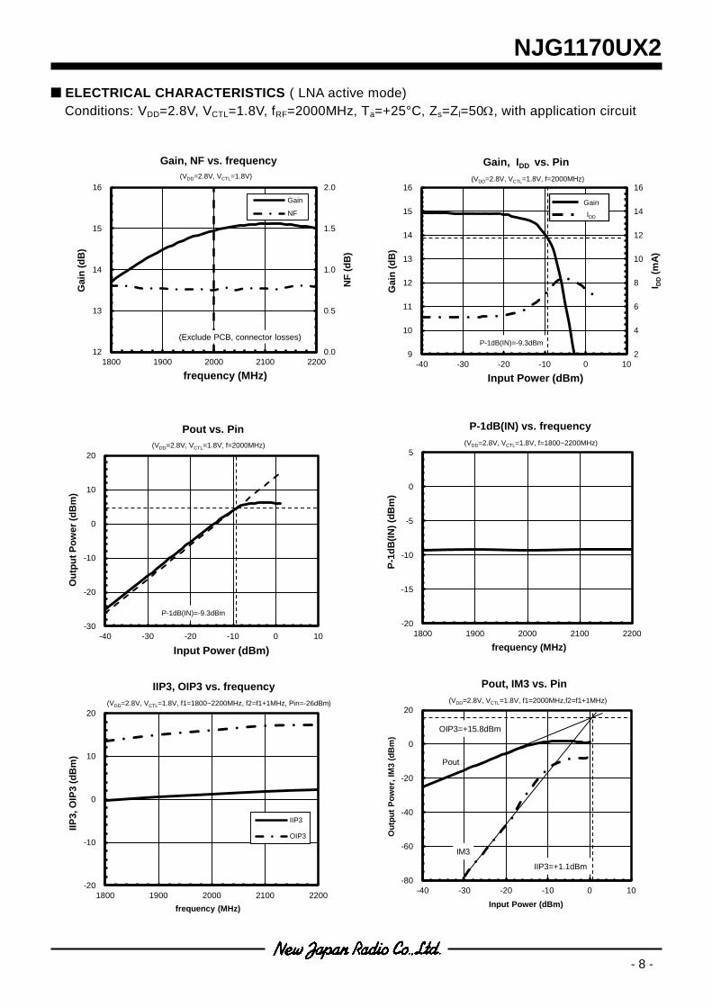
ELECTRICAL CHARACTERISTICS ( LNA active mode)
Conditions: VDD=2.8V, VCTL=1.8V, fRF=2000MHz, Ta=+25°C, Zs=Zl=50, with application circuit
0.0
0.5
1.0
1.5
2.0
12
13
14
15
16
1800 1900 2000 2100 2200
NF
(d
B)
Gain
(d
B)
frequency (MHz)
Gain, NF vs. frequency
Gain
NF
(Exclude PCB, connector losses)
(VDD=2.8V, VCTL=1.8V)
2
4
6
8
10
12
14
16
9
10
11
12
13
14
15
16
-40 -30 -20 -10 0 10
I DD (
mA
)
Gain
(d
B)
Input Power (dBm)
Gain, IDD vs. Pin
(VDD=2.8V, VCTL=1.8V, f=2000MHz)
P-1dB(IN)=-9.3dBm
Gain
IDD
-30
-20
-10
0
10
20
-40 -30 -20 -10 0 10
Ou
tpu
t P
ow
er
(dB
m)
Input Power (dBm)
Pout vs. Pin
(VDD=2.8V, VCTL=1.8V, f=2000MHz)
P-1dB(IN)=-9.3dBm
-20
-15
-10
-5
0
5
1800 1900 2000 2100 2200
P-1
dB
(IN
) (d
Bm
)
frequency (MHz)
P-1dB(IN) vs. frequency
(VDD=2.8V, VCTL=1.8V, f=1800~2200MHz)
-20
-10
0
10
20
1800 1900 2000 2100 2200
IIP
3, O
IP3 (
dB
m)
frequency (MHz)
IIP3, OIP3 vs. frequency
IIP3
OIP3
(VDD=2.8V, VCTL=1.8V, f1=1800~2200MHz, f2=f1+1MHz, Pin=-26dBm)
-80
-60
-40
-20
0
20
-40 -30 -20 -10 0 10
Ou
tpu
t P
ow
er,
IM
3 (
dB
m)
Input Power (dBm)
Pout, IM3 vs. Pin
(VDD=2.8V, VCTL=1.8V, f1=2000MHz,f2=f1+1MHz)
Pout
IM3
OIP3=+15.8dBm
IIP3=+1.1dBm

NJG1170UX2
- 9 -
ELECTRICAL CHARACTERISTICS ( LNA active mode)
Conditions:
VDD=2.8V, VCTL=1.8V, fRF=50 to 6000MHz, Ta=+25°C, Zs=Zl=50, with application circuit
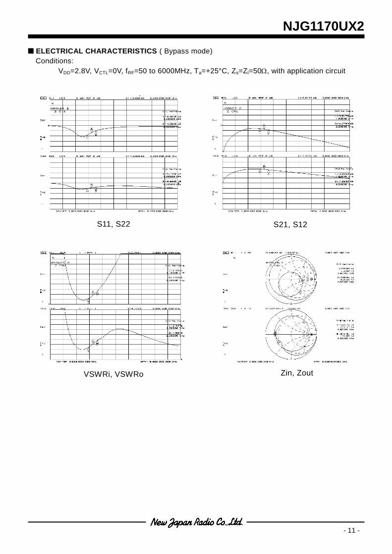
S11, S22
Zin, Zout VSWRi, VSWRo
S21, S12

NJG1170UX2
- 10 -
ELECTRICAL CHARACTERISTICS ( Bypass mode)
Conditions: VDD=2.8V, VCTL=0V, fRF=2000MHz, Ta=+25°C, Zs=Zl=50, with application circuit
0
1
2
3
4
5
6
1800 1900 2000 2100 2200
Lo
ss (
dB
)
frequency (MHz)
Loss vs. frequency
(VDD=2.8V, VCTL=0V)
(Exclude PCB, connector losses)
0
10
20
30
40
500
2
4
6
8
10
-20 -10 0 10 20
I DD
(uA
)
Lo
ss (
dB
)Input Power (dBm)
Loss, IDD vs. Pin
(VDD=2.8V, VCTL=0V, f=2000MHz)
P-1dB(IN)=+10.1dBm
Gain
IDD
-30
-20
-10
0
10
20
-20 -10 0 10 20
Ou
tpu
t P
ow
er
(dB
m)
Input Power (dBm)
Pout vs. Pin
(VDD=2.8V, VCTL=0V, f=2000MHz)
P-1dB(IN)=+10.1dBm
-20
-10
0
10
20
1800 1900 2000 2100 2200
P-1
dB
(IN
) (d
Bm
)
frequency (MHz)
P-1dB(IN) vs. frequency
(VDD=2.8V, VCTL=0V, f=1800~2200MHz)
0
10
20
30
40
1800 1900 2000 2100 2200
IIP
3, O
IP3 (
dB
m)
frequency (MHz)
IIP3, OIP3 vs. frequency
IIP3
OIP3
(VDD=2.8V, VCTL=0V, f1=1800~2200MHz, f2=f1+1MHz, Pin=-15dBm)
-80
-60
-40
-20
0
20
-20 -10 0 10 20
Ou
tpu
t P
ow
er,
IM
3 (
dB
m)
Input Power (dBm)
Pout, IM3 vs. Pin
(VDD=2.8V, VCTL=0V, f1=2000MHz,f2=f1+1MHz)
Pout
IM3
OIP3=+13.2dBm
IIP3=+16.8dBm
NJG1170UX2
- 11 -
ELECTRICAL CHARACTERISTICS ( Bypass mode)
Conditions:
VDD=2.8V, VCTL=0V, fRF=50 to 6000MHz, Ta=+25°C, Zs=Zl=50, with application circuit
S11, S22 S21, S12
VSWRi, VSWRo Zin, Zout

NJG1170UX2
- 12 -
ELECTRICAL CHARACTERISTICS ( LNA active mode)
Conditions: VDD=2.8V, VCTL=1.8V, fRF=2500MHz, Ta=+25°C, Zs=Zl=50, with application circuit
0
0.5
1
1.5
2
10
11
12
13
14
15
16
2200 2300 2400 2500 2600 2700 2800
NF
(d
B)
Gain
(d
B)
frequency (MHz)
Gain, NF vs. frequency
Gain
NF
(Exclude PCB, connector losses)
(VDD=2.8V, VCTL=1.8V)
2
4
6
8
10
12
14
16
9
10
11
12
13
14
15
16
-40 -30 -20 -10 0 10
I DD
(mA
)
Gain
(d
B)
Input Power (dBm)
Gain, IDD vs. Pin
(VDD=2.8V, VCTL=1.8V, f=2500MHz)
P-1dB(IN)=-8.5dBm
Gain
IDD
-30
-20
-10
0
10
20
-40 -30 -20 -10 0 10
Ou
tpu
t P
ow
er
(dB
m)
Input Power (dBm)
Pout vs. Pin
(VDD=2.8V, VCTL=1.8V, f=2500MHz)
P-1dB(IN)=-8.5dBm
-20
-15
-10
-5
0
5
2300 2400 2500 2600 2700
P-1
dB
(IN
) (d
Bm
)
frequency (MHz)
P-1dB(IN) vs. frequency
(VDD=2.8V, VCTL=1.8V, f=2300~2700MHz)
0
5
10
15
20
25
2300 2400 2500 2600 2700
IIP
3, O
IP3
(d
Bm
)
frequency (MHz)
IIP3, OIP3 vs. frequency
IIP3
OIP3
(VDD=2.8V, VCTL=1.8V, f1=2300~2700MHz, f2=f1+1MHz, Pin=-26dBm)
-80
-60
-40
-20
0
20
-40 -30 -20 -10 0 10
Ou
tpu
t P
ow
er,
IM
3 (
dB
m)
Input Power (dBm)
Pout, IM3 vs. Pin
(VDD=2.8V, VCTL=1.8V, f1=2500MHz,f2=f1+1MHz)
Pout
IM3
OIP3=+17.5dBm
IIP3=+3.3dBm
NJG1170UX2
- 13 -
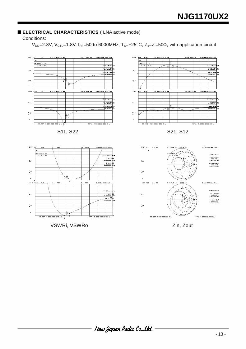
ELECTRICAL CHARACTERISTICS ( LNA active mode)
Conditions:
VDD=2.8V, VCTL=1.8V, fRF=50 to 6000MHz, Ta=+25°C, Zs=Zl=50, with application circuit
S11, S22 S21, S12
VSWRi, VSWRo Zin, Zout

NJG1170UX2
- 14 -
ELECTRICAL CHARACTERISTICS ( Bypass mode)
Conditions: VDD=2.8V, VCTL=0V, fRF=2500MHz, Ta=+25°C, Zs=Zl=50, with application circuit
0
1
2
3
4
5
6
2200 2300 2400 2500 2600 2700 2800
Lo
ss (
dB
)
frequency (MHz)
Loss vs. frequency
(VDD=2.8V, VCTL=0V)
(Exclude PCB, connector losses)
0
5
10
15
20
25
30
35
40
45
500
1
2
3
4
5
6
7
8
9
10
-20 -10 0 10 20
I DD
(uA
)
Lo
ss (
dB
)
Input Power (dBm)
Loss, IDD vs. Pin
(VDD=2.8V, VCTL=0V, f=2500MHz)
P-1dB(IN)=+9.9dBm
Loss
IDD
-10
-5
0
5
10
15
20
2200 2300 2400 2500 2600 2700 2800
P-1
dB
(IN
) (d
Bm
)
frequency (MHz)
P-1dB(IN) vs. frequency
(VDD=2.8V, VCTL=0V, f=2300~2700MHz)
0
10
20
30
40
2200 2300 2400 2500 2600 2700 2800
IIP
3, O
IP3 (
dB
m)
frequency (MHz)
IIP3, OIP3 vs. frequency
IIP3
OIP3
(VDD=2.8V, VCTL=0V, f1=2300~2700MHz, f2=f1+1MHz, Pin=-15dBm)
-30
-20
-10
0
10
20
-20 -10 0 10 20
Ou
tpu
t P
ow
er
(dB
m)
Input Power (dBm)
Pout vs. Pin
(VDD=2.8V, VCTL=0V, f=2500MHz)
P-1dB(IN)=+9.9dBm
-100
-80
-60
-40
-20
0
20
-20 -10 0 10 20
Ou
tpu
t P
ow
er,
IM
3 (
dB
m)
Input Power (dBm)
Pout, IM3 vs. Pin
(VDD=2.8V, VCTL=0V, f1=2500MHz,f2=f1+1MHz)
Pout
IM3
OIP3=+14.0dBm
IIP3=+17.0dBm
NJG1170UX2
- 15 -
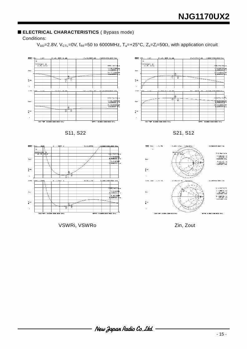
ELECTRICAL CHARACTERISTICS ( Bypass mode)
Conditions:
VDD=2.8V, VCTL=0V, fRF=50 to 6000MHz, Ta=+25°C, Zs=Zl=50, with application circuit
S11, S22 S21, S12
VSWRi, VSWRo Zin, Zout

NJG1170UX2
- 16 -
APPLICATION CIRCUIT
PARTS LIST
Parts ID Value Manufacture
L1
7.5nH (1805MHz to 2200MHz)
LQW15AN_00 Series (MURATA) 4.7nH
(2300MHz to 2690MHz)
C1 1000pF GRM03 Series (MURATA)
VCTL
(Top View)
RFIN VDD
RFOUT
L1
C1
1 Pin INDEX
NJG1170UX2
- 17 -
NOISE FIGURE MEASUREMENT BLOCK DIAGRAM
Measuring instruments
NF Analyzer : Keysight 8973A
Noise Source : Keysight 346A
Setting the NF analyzer
Measurement mode form
Device under test : Amplifier
System downconverter : off
Mode setup form
Sideband : LSB
Averages : 8
Average mode : Point
Bandwidth : 4MHz
Loss comp : off
Tcold : setting the temperature of noise source (305.15K)
Calibration setup
Noise Source (Keysight 346A)
NF Analyzer (Keysight 8973A)
Input (50) Noise Source Drive Output
* Preamplifier is used to improve
NF measurement accuracy.
* Noise source, preamplifier and
NF analyzer are connected
directly.
Preamplifier AVAGO VMMK-2103
Gain 15dB
NF 2.0dB
Measurement Setup
Noise Source (Keysight 346A)
DUT
NF Analyzer (Keysight 8973A)
Input (50) Noise Source Drive Output
IN OUT
* Noise source, DUT,preamplifier
and NF analyzer are connected
directly.
Preamplifier AVAGO VMMK-2130
Gain 15dB
NF 2.0dB
NJG1170UX2
- 18 -
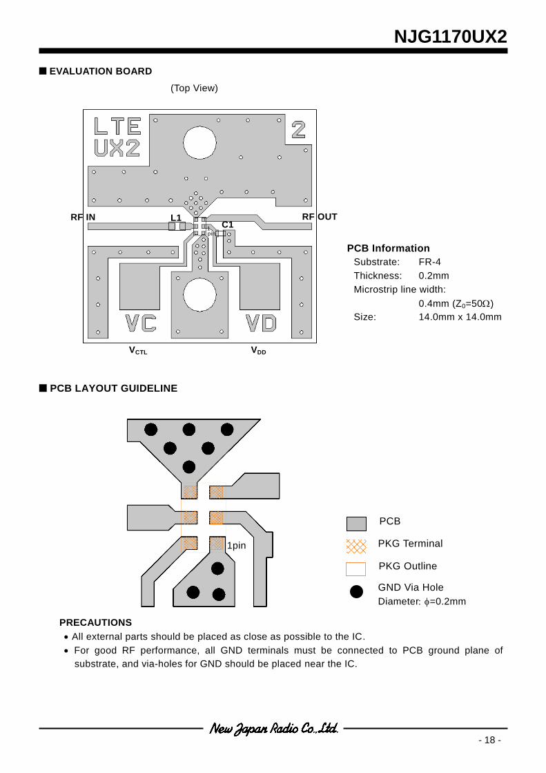
EVALUATION BOARD
PCB LAYOUT GUIDELINE
PRECAUTIONS
All external parts should be placed as close as possible to the IC.
For good RF performance, all GND terminals must be connected to PCB ground plane of
substrate, and via-holes for GND should be placed near the IC.
L1 C1
RF IN RF OUT
VDD VCTL
1 pin
(Top View)
PCB Information
Substrate: FR-4
Thickness: 0.2mm
Microstrip line width:
0.4mm (Z0=50)
Size: 14.0mm x 14.0mm
1pin
GND Via Hole
Diameter=0.2mm
PKG Terminal
PCB
PKG Outline
NJG1170UX2
- 19 -
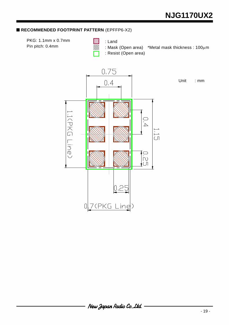
RECOMMENDED FOOTPRINT PATTERN (EPFFP6-X2)
: Land
: Mask (Open area) *Metal mask thickness : 100m
: Resist (Open area)
PKG: 1.1mm x 0.7mm
Pin pitch: 0.4mm
Unit : mm

NJG1170UX2
- 20 -
PACKAGE OUTLINE (EPFFP6-X2)
Cautions on using this product This product contains Gallium-Arsenide (GaAs) which is a harmful material.
Do NOT eat or put into mouth.
Do NOT dispose in fire or break up this product.
Do NOT chemically make gas or powder with this product.
To waste this product, please obey the relating law of your country.
This product may be damaged with electric static discharge (ESD) or spike voltage. Please handle with care to avoid these damages.
[CAUTION] The specifications on this databook are only given for information , without any guarantee as regards either mistakes or omissions. The application circuits in this databook are described only to show representative usages of the product and not intended for the guarantee or
permission of any right including the industrial rights.
Unit : mm
Substrate : FR4
Terminal treat : Ni/Pd/Au
Molding material : Epoxy resin
Weight (typ.) : 0.7mg
TOP VIEW
SIDE VIEW
BOTTOM VIEW


