
IEEE 802.3 GEPOF Study Group - May 2014 Interim
POF
Knowledge Development
Rubén Pé[email protected]
Optical receiver characteristics analysis for GEPOF technical feasibility
IEEE 802.3 GEPOF Study Group - May 2014 Interim
POF
Knowledge Development
Supporters• Frank Aldinger (Mitsubishi International)
• Yutaka Tanida (Mitsubishi Corporation)
• Y.Tsukamoto (Mitsubishi Rayon)
• Eric Chan (Boeing)
• Philippe Bolle (Skylaneoptics)
• 曹�文 / Mike Cao (Dongguan ipt Industrial Co,.LTD.)
• John Lambkin (Firecomms)
• Hugh Hennessy (Firecomms)
• Josef Faller (Homefibre)
• Manabu Kagami (Toyota R&D Labs)
• Bas Huiszoon (Genexis)
• Oscar Rechou (Casacom)
• Naoshi Serizawa (Yazaki)
• Thomas Lichtenegger (Avago Tech)
2
IEEE 802.3 GEPOF Study Group - May 2014 Interim
POF
Knowledge Development
Agenda• Objectives
• The optical receiver
• Characteristics of photodiodes used in POF communications
• Trans-impedance amplifier limits and performance
• Conclusions
3
IEEE 802.3 GEPOF Study Group - May 2014 Interim
POF
Knowledge Development
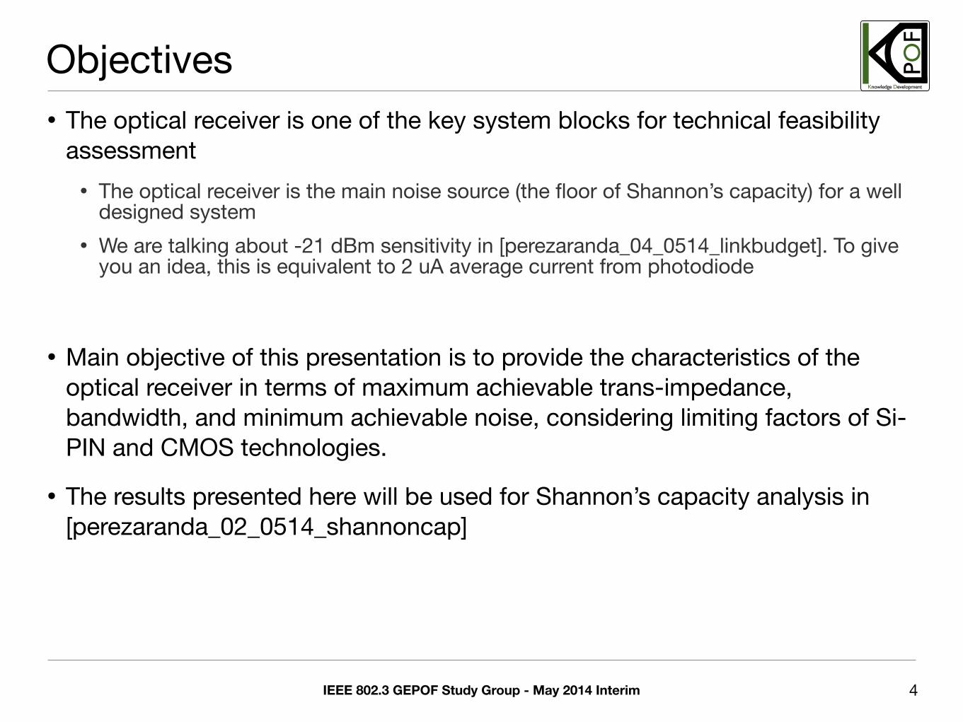
Objectives• The optical receiver is one of the key system blocks for technical feasibility
assessment• The optical receiver is the main noise source (the floor of Shannon’s capacity) for a well
designed system• We are talking about -21 dBm sensitivity in [perezaranda_04_0514_linkbudget]. To give
you an idea, this is equivalent to 2 uA average current from photodiode
• Main objective of this presentation is to provide the characteristics of the optical receiver in terms of maximum achievable trans-impedance, bandwidth, and minimum achievable noise, considering limiting factors of Si-PIN and CMOS technologies.
• The results presented here will be used for Shannon’s capacity analysis in [perezaranda_02_0514_shannoncap]
4
IEEE 802.3 GEPOF Study Group - May 2014 Interim
POF
Knowledge Development
Disclaimer• Technical characteristics provided in this presentation are a collection of
confidential information from several IC foundries, therefore sources will not be revealed.
• However, the characteristics of devices presented here are very common to several technology nodes from several years ago ➤ they are not in the state of art
5
IEEE 802.3 GEPOF Study Group - May 2014 Interim
POF
Knowledge Development
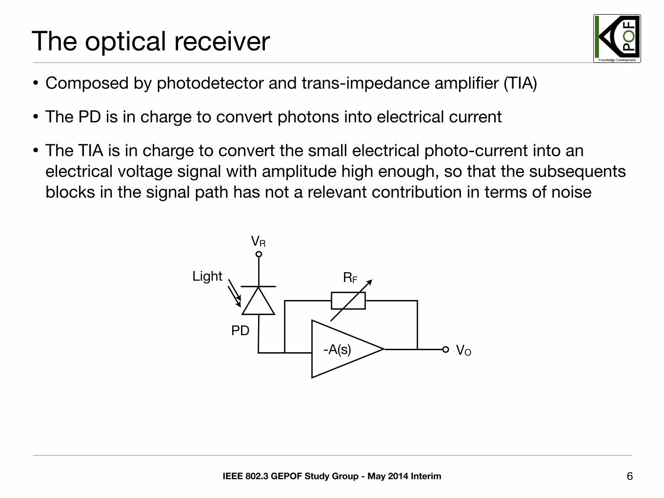
The optical receiver• Composed by photodetector and trans-impedance amplifier (TIA)
• The PD is in charge to convert photons into electrical current
• The TIA is in charge to convert the small electrical photo-current into an electrical voltage signal with amplitude high enough, so that the subsequents blocks in the signal path has not a relevant contribution in terms of noise
6
-A(s)PD
RF
VO
Light
VR
IEEE 802.3 GEPOF Study Group - May 2014 Interim
POF
Knowledge Development
The optical receiver
7
• Light to current conversion is linear, provided that the electrical current of the communication signal is higher enough than PD dark current characteristic
• In general, the TIA I-V conversion has to be linear to enable using advance modulation schemes ➤ for Shannon’s capacity analysis can be considered linear
• Linear TIAs are implemented by integrating trans-impedance automatic control as a function of input photo-current to avoid transistors overloading
• For 650 nm POF applications, the PD is typically a Si-PIN
• 2 typical implementations:• PD and TIA are two separated ICs fabricated using different technology processes; both
are connected in a lead-frame by using bonding wires• PD and TIA are fabricated in a single Opto-electronic IC (OEIC), improving SRR, EMI and
ESD characteristics of optical RX and reducing manufacturing cost• Both implementations have been demonstrated to be good for MOST150 automotive
applications
IEEE 802.3 GEPOF Study Group - May 2014 Interim
POF
Knowledge Development
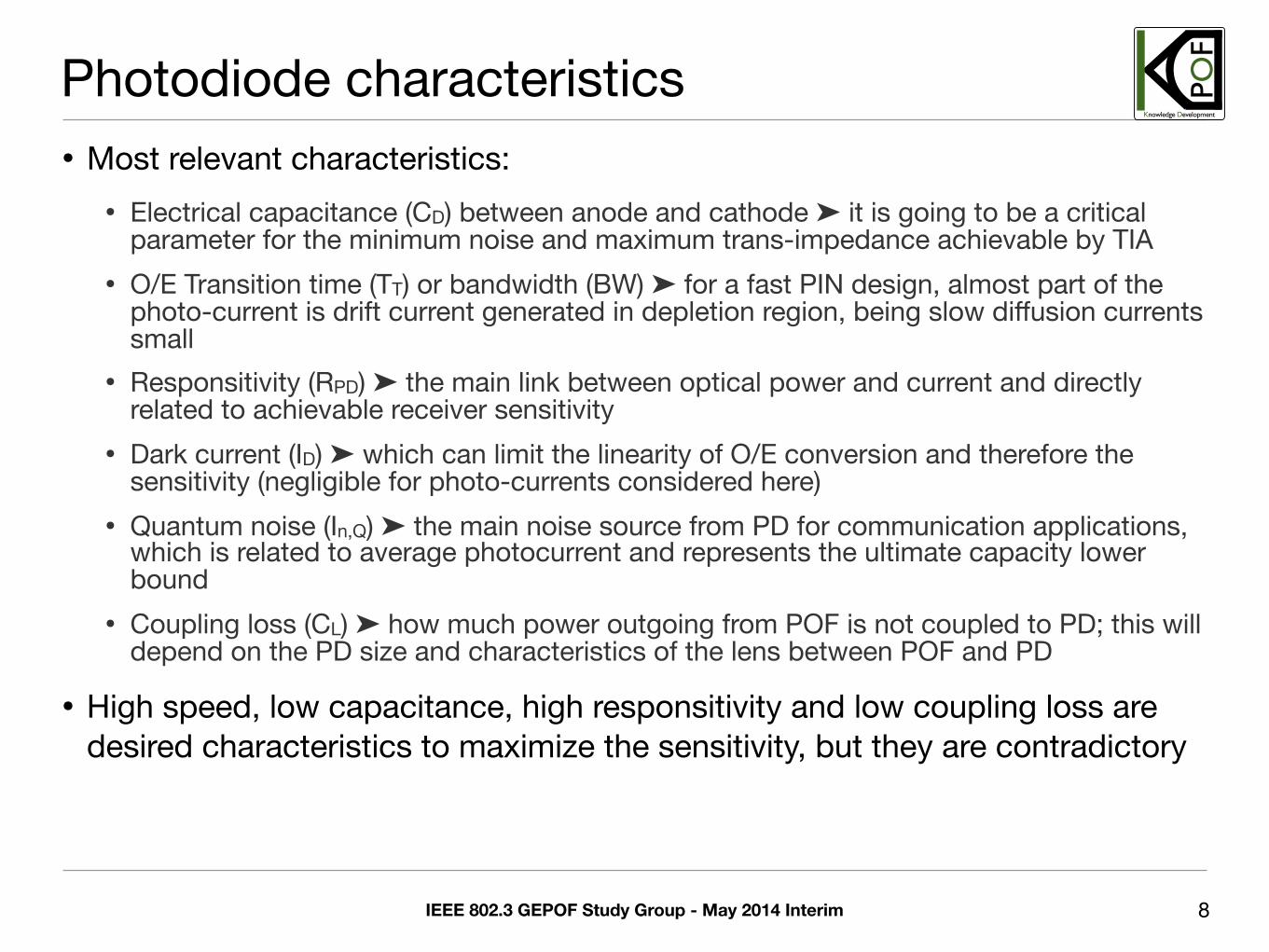
Photodiode characteristics• Most relevant characteristics:
• Electrical capacitance (CD) between anode and cathode ➤ it is going to be a critical parameter for the minimum noise and maximum trans-impedance achievable by TIA
• O/E Transition time (TT) or bandwidth (BW) ➤ for a fast PIN design, almost part of the photo-current is drift current generated in depletion region, being slow diffusion currents small
• Responsitivity (RPD) ➤ the main link between optical power and current and directly related to achievable receiver sensitivity
• Dark current (ID) ➤ which can limit the linearity of O/E conversion and therefore the sensitivity (negligible for photo-currents considered here)
• Quantum noise (In,Q) ➤ the main noise source from PD for communication applications, which is related to average photocurrent and represents the ultimate capacity lower bound
• Coupling loss (CL) ➤ how much power outgoing from POF is not coupled to PD; this will depend on the PD size and characteristics of the lens between POF and PD
• High speed, low capacitance, high responsitivity and low coupling loss are desired characteristics to maximize the sensitivity, but they are contradictory
8
IEEE 802.3 GEPOF Study Group - May 2014 Interim
POF
Knowledge Development
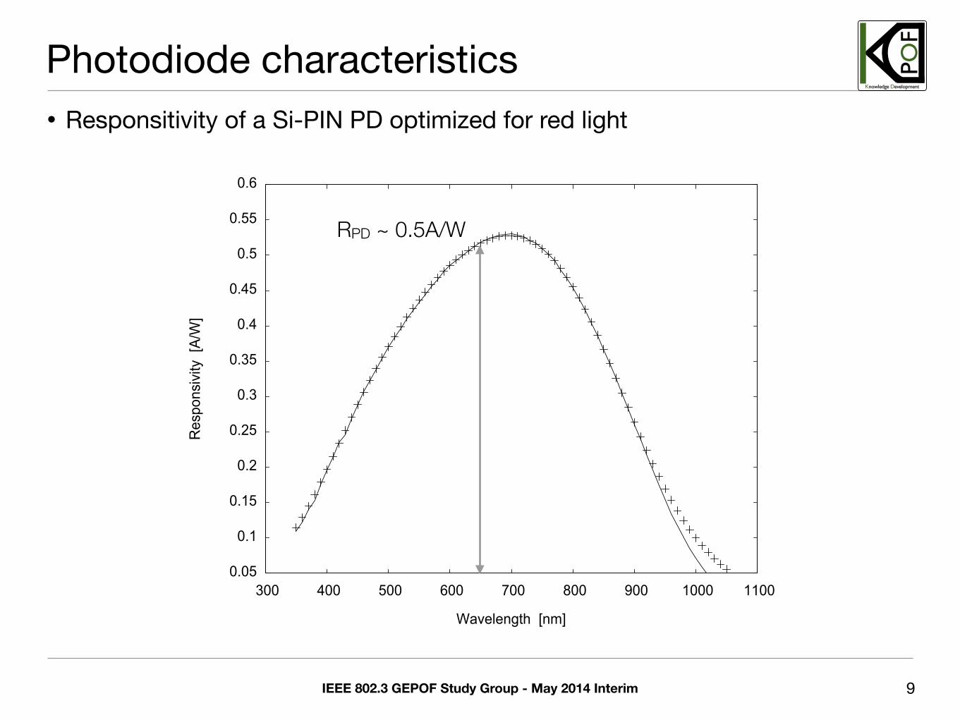
Photodiode characteristics
9
Process & Device Specification XO035
PDS_035_08 Release 2.1.1
Page 108 of 112 CompanyConfidential
6.5. Photo Diode Characteristics
0.05
0.10
0.15
0.20
0.25
0.30
0.35
0.40
0.45
0.50
300 400 500 600 700 800 900 1000 1100
Re
sp
on
siv
ity
[A/W
]
Wavelength [nm]
Figure 6.15 Device dpinb: Spectral responsivity characteristic for a typical wafer + = measured, solid line = model
0.05
0.1
0.15
0.2
0.25
0.3
0.35
0.4
0.45
0.5
0.55
0.6
300 400 500 600 700 800 900 1000 1100
Re
spo
nsi
vity
[A
/W]
Wavelength [nm]
Figure 6.16 Device dpinbr: Spectral responsivity characteristic for a typical wafer + = measured, solid line = model
• Responsitivity of a Si-PIN PD optimized for red light
RPD ~ 0.5A/W
IEEE 802.3 GEPOF Study Group - May 2014 Interim
POF
Knowledge Development
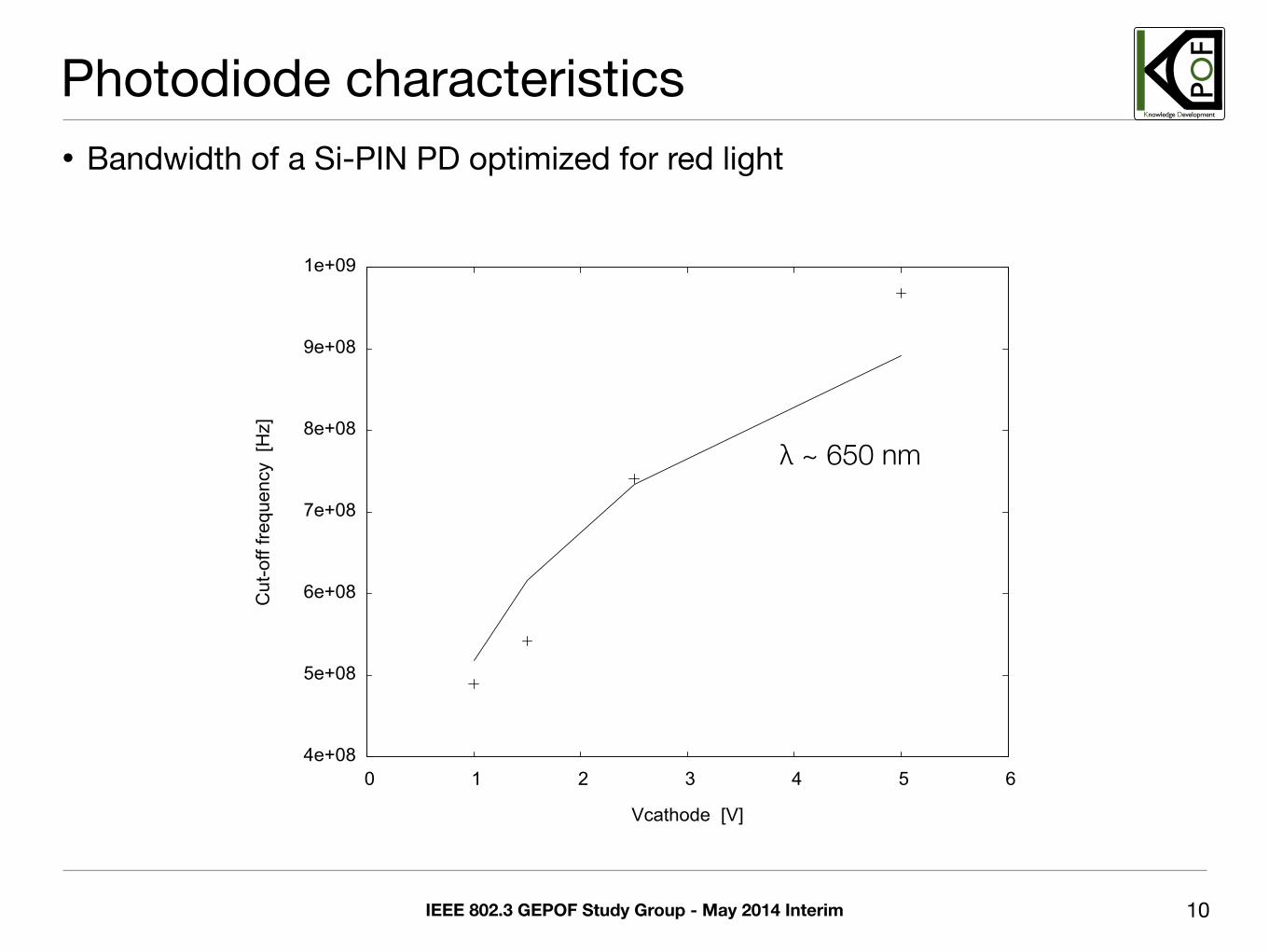
Photodiode characteristics• Bandwidth of a Si-PIN PD optimized for red light
10
Process & Device Specification XO035
PDS_035_08 Release 2.1.1
Page 110 of 112 CompanyConfidential
4e+08
5e+08
6e+08
7e+08
8e+08
9e+08
1e+09
0 1 2 3 4 5 6
Cut
-off
frequ
ency
[H
z]
Vcathode [V]
Figure 6.19 Device dpinbr: Cut-off frequency vs. cathode voltage for a typical wafer W=L=100µm, wavelength = 636nm, + = measured, solid line = model Note: Modeling of the cut-off-frequency in the infrared regime is not supported.
0
2e+08
4e+08
6e+08
8e+08
1e+09
300 400 500 600 700 800 900 1000 1100
Cut
-off
frequ
ency
[H
z]
Wavelength [nm]
Figure 6.20 Device dpinb, dpinbr, dpinbir: Cut-off frequency vs. wavelength for a typical wafer W=L=100µm, Vcathode = 2.5V, + = measured, solid line = model
λ ~ 650 nm
IEEE 802.3 GEPOF Study Group - May 2014 Interim
POF
Knowledge Development
Photodiode characteristics
11
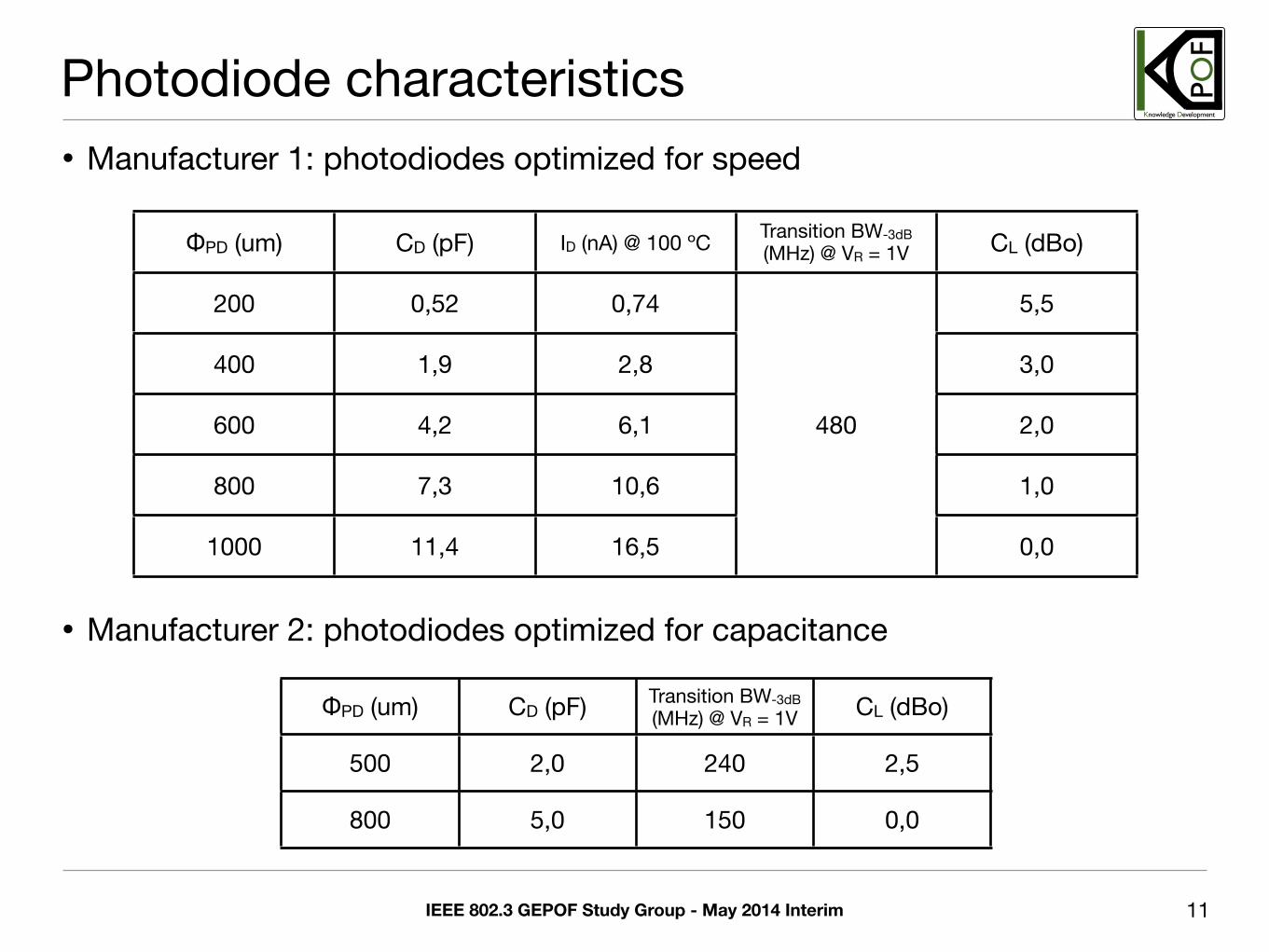
ΦPD (um) CD (pF) ID (nA) @ 100 ºC Transition BW-3dB (MHz) @ VR = 1V CL (dBo)
200 0,52 0,74
480
5,5
400 1,9 2,8
480
3,0
600 4,2 6,1 480 2,0
800 7,3 10,6
480
1,0
1000 11,4 16,5
480
0,0
ΦPD (um) CD (pF) Transition BW-3dB (MHz) @ VR = 1V CL (dBo)
500 2,0 240 2,5
800 5,0 150 0,0
• Manufacturer 1: photodiodes optimized for speed
• Manufacturer 2: photodiodes optimized for capacitance
IEEE 802.3 GEPOF Study Group - May 2014 Interim
POF
Knowledge Development
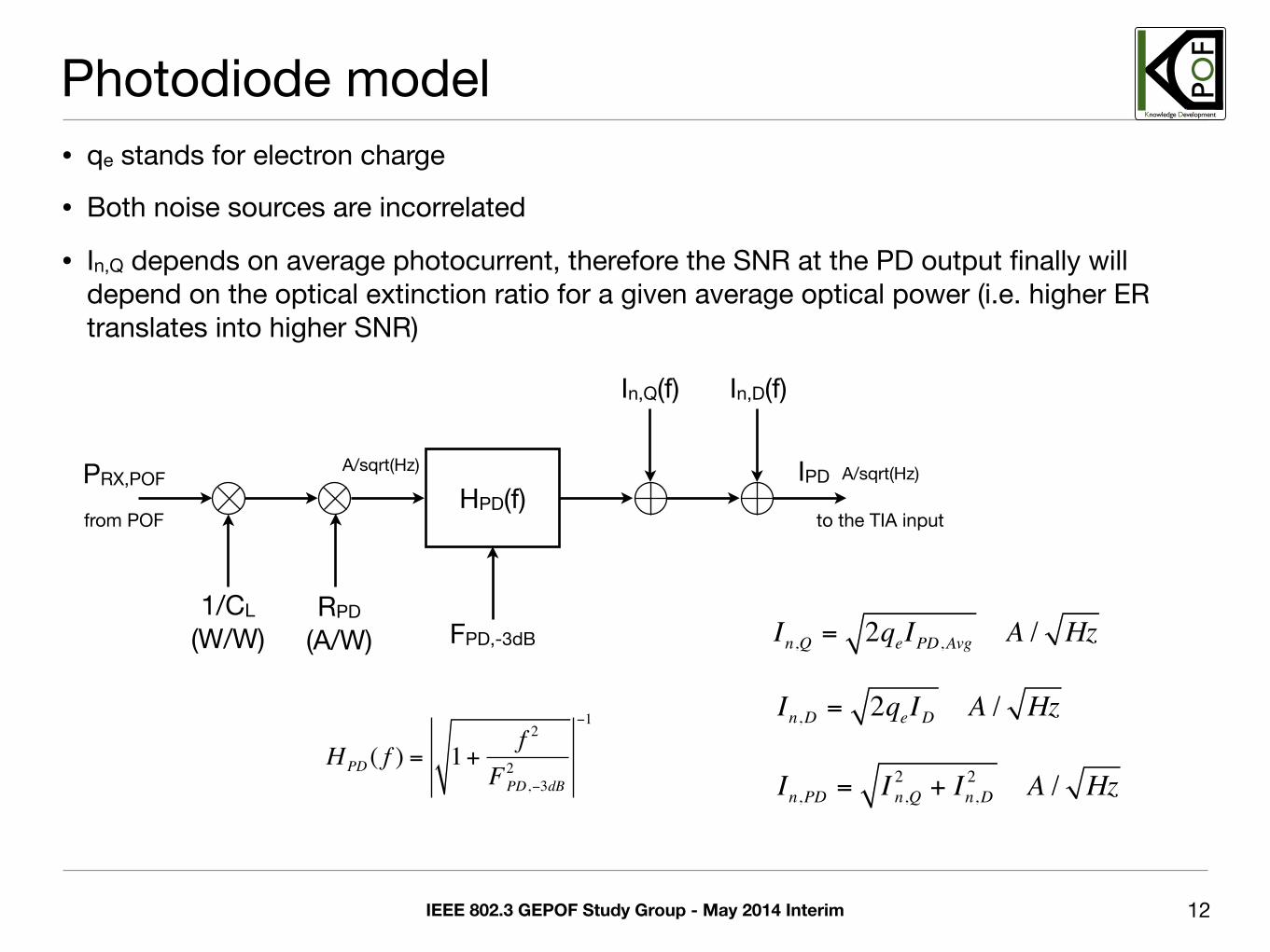
Photodiode model
12
HPD(f)PRX,POF
1/CL(W/W)
RPD(A/W)
In,Q(f) In,D(f)
IPD
to the TIA inputfrom POF
FPD,-3dB
A/sqrt(Hz) A/sqrt(Hz)
HPD ( f ) = 1+ f 2
F2PD,−3dB
−1
In,Q = 2qeIPD,Avg A / Hz
In,D = 2qeID A / Hz
In,PD = I 2n,Q + In,D2 A / Hz
• qe stands for electron charge
• Both noise sources are incorrelated
• In,Q depends on average photocurrent, therefore the SNR at the PD output finally will depend on the optical extinction ratio for a given average optical power (i.e. higher ER translates into higher SNR)
IEEE 802.3 GEPOF Study Group - May 2014 Interim
POF
Knowledge Development
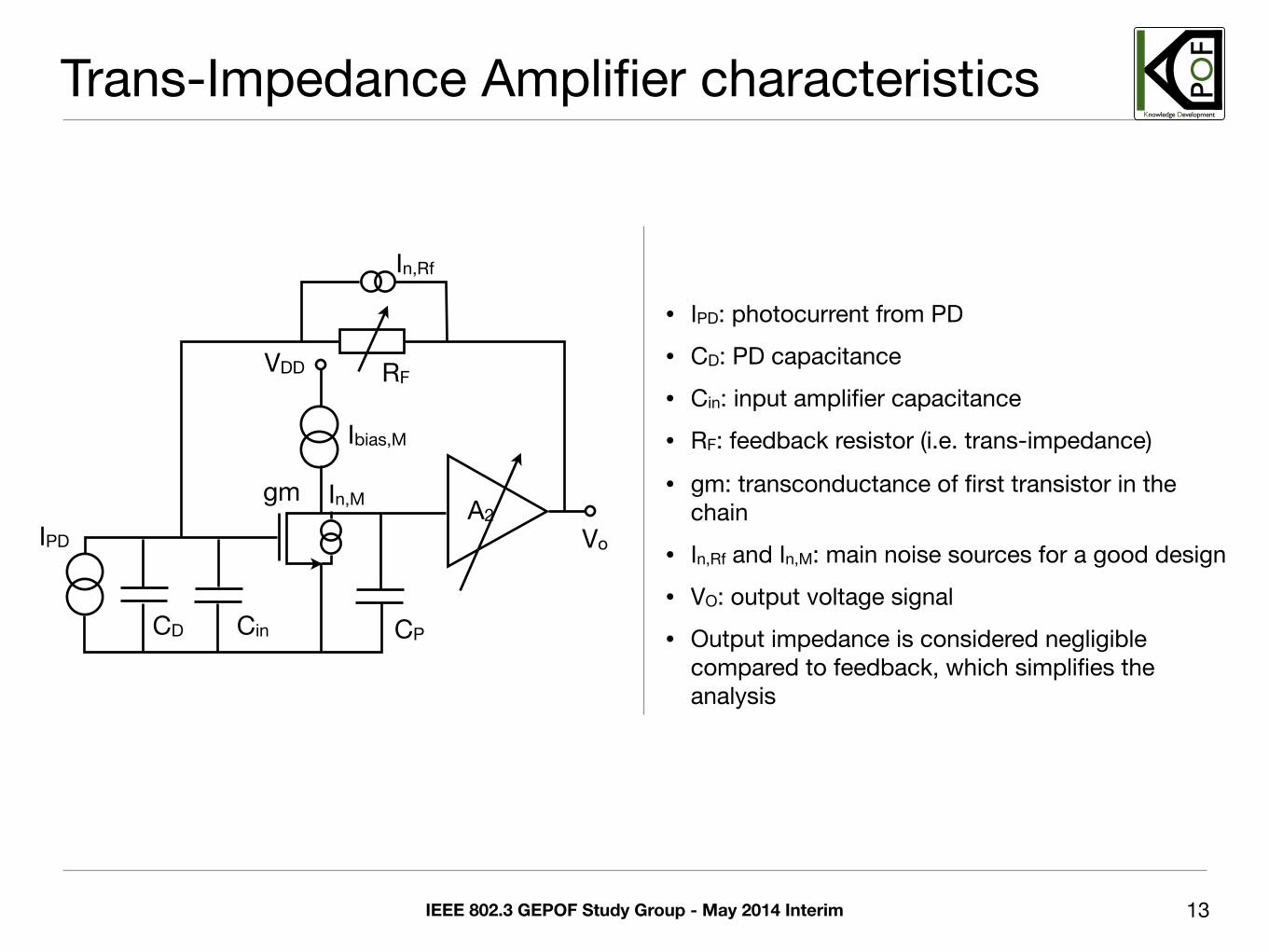
Trans-Impedance Amplifier characteristics
13
A2
RF
IPD
In,Rf
CinCD
In,M
Ibias,M
gm
VDD
CP
• IPD: photocurrent from PD
• CD: PD capacitance
• Cin: input amplifier capacitance
• RF: feedback resistor (i.e. trans-impedance)
• gm: transconductance of first transistor in the chain
• In,Rf and In,M: main noise sources for a good design
• VO: output voltage signal
• Output impedance is considered negligible compared to feedback, which simplifies the analysis
Vo
IEEE 802.3 GEPOF Study Group - May 2014 Interim
POF
Knowledge Development
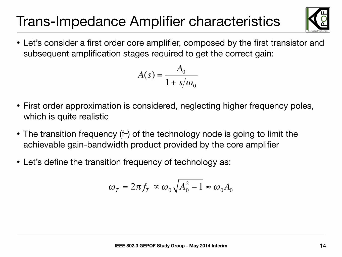
Trans-Impedance Amplifier characteristics• Let’s consider a first order core amplifier, composed by the first transistor and
subsequent amplification stages required to get the correct gain:
• First order approximation is considered, neglecting higher frequency poles, which is quite realistic
• The transition frequency (fT) of the technology node is going to limit the achievable gain-bandwidth product provided by the core amplifier
• Let’s define the transition frequency of technology as:
14
A(s) = A01+ s ω0
ωT = 2π fT ∝ω0 A20 −1 ≈ω0A0
IEEE 802.3 GEPOF Study Group - May 2014 Interim
POF
Knowledge Development
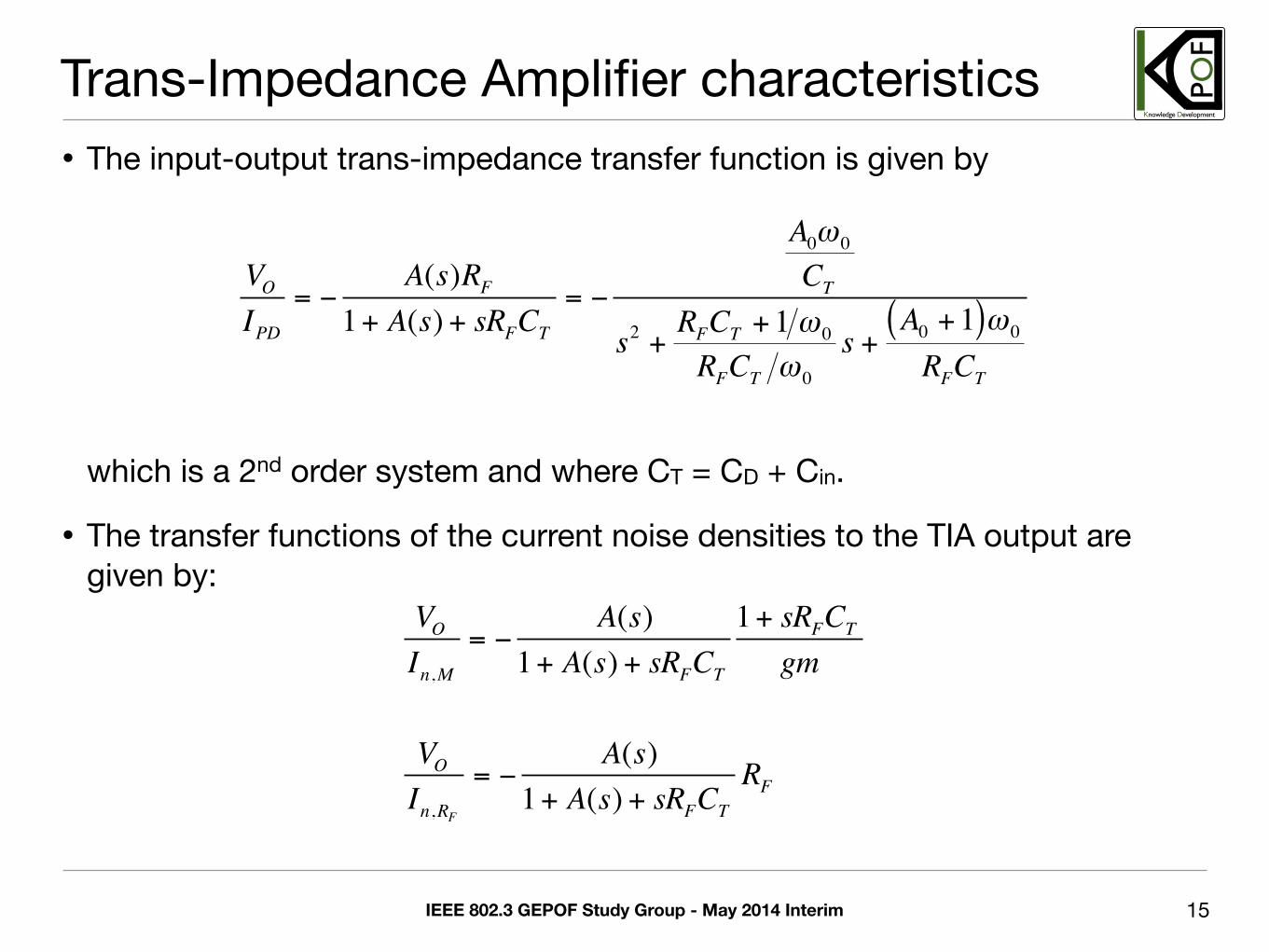
Trans-Impedance Amplifier characteristics• The input-output trans-impedance transfer function is given by
which is a 2nd order system and where CT = CD + Cin.
• The transfer functions of the current noise densities to the TIA output are given by:
15
VOIPD
= −A(s)RF
1+ A(s) + sRFCT
= −
A0ω0
CT
s2 + RFCT +1 ω0
RFCT ω0
s +A0 +1( )ω0
RFCT
VOIn,M
= −A(s)
1+ A(s) + sRFCT
1+ sRFCT
gm
VOIn,RF
= −A(s)
1+ A(s) + sRFCT
RF
IEEE 802.3 GEPOF Study Group - May 2014 Interim
POF
Knowledge Development
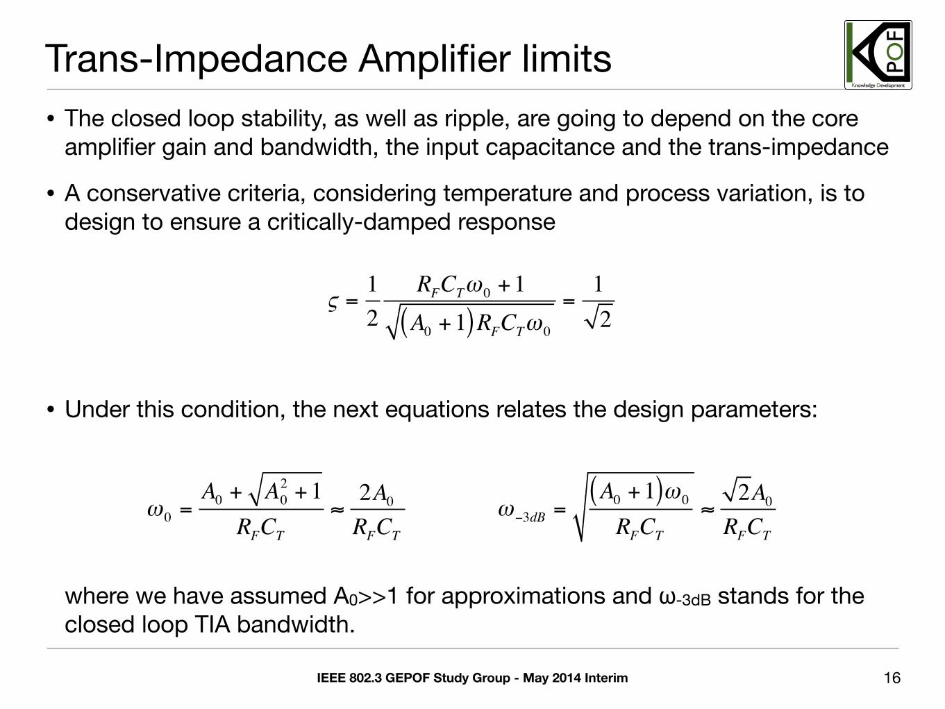
Trans-Impedance Amplifier limits• The closed loop stability, as well as ripple, are going to depend on the core
amplifier gain and bandwidth, the input capacitance and the trans-impedance
• A conservative criteria, considering temperature and process variation, is to design to ensure a critically-damped response
• Under this condition, the next equations relates the design parameters:
where we have assumed A0>>1 for approximations and ω-3dB stands for the closed loop TIA bandwidth.
16
ς =12
RFCTω0 +1A0 +1( )RFCTω0
=12
ω0 =A0 + A20 +1
RFCT
≈2A0RFCT
ω−3dB =A0 +1( )ω0
RFCT
≈2A0
RFCT
IEEE 802.3 GEPOF Study Group - May 2014 Interim
POF
Knowledge Development
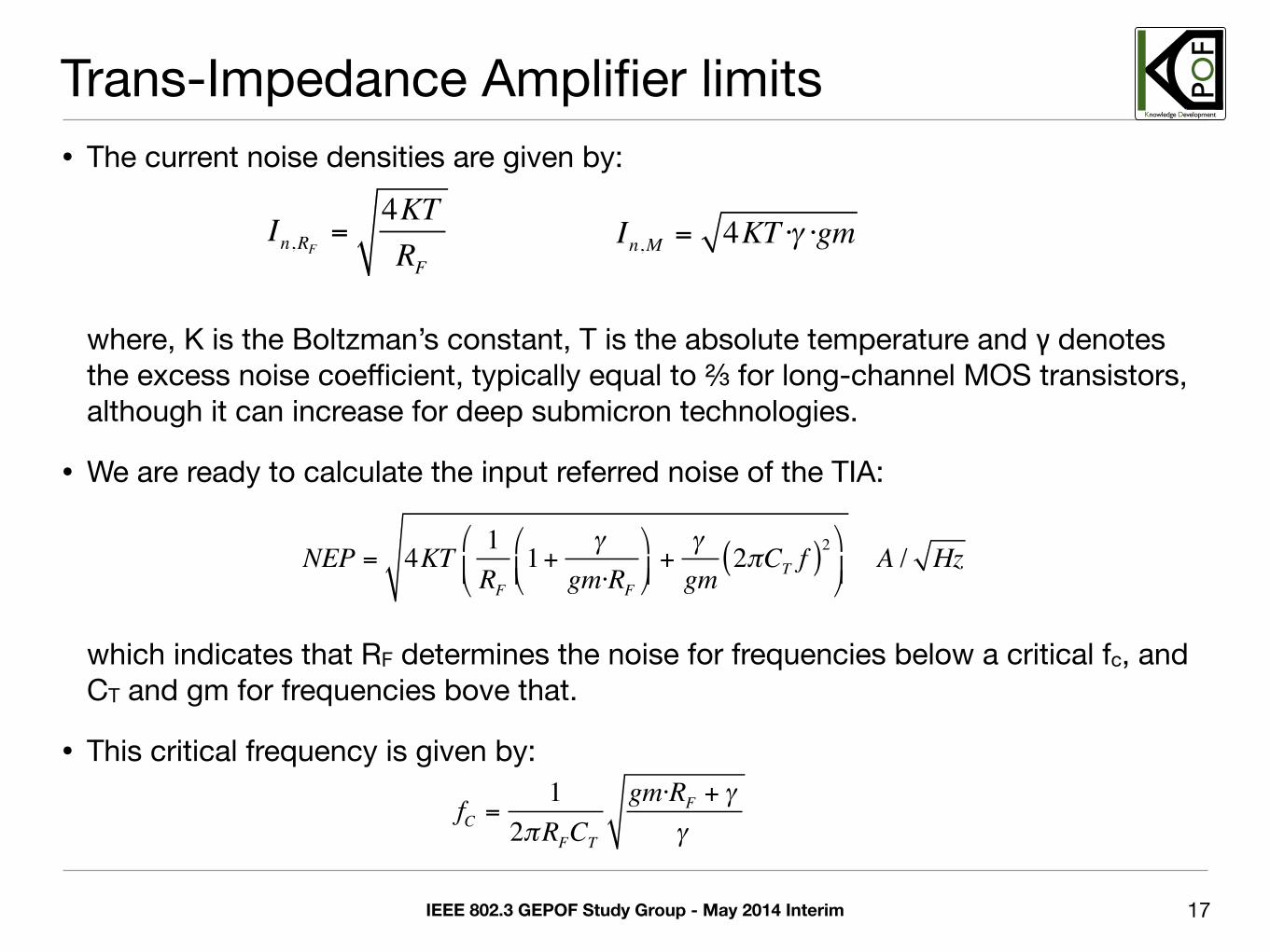
Trans-Impedance Amplifier limits• The current noise densities are given by:
where, K is the Boltzman’s constant, T is the absolute temperature and γ denotes the excess noise coefficient, typically equal to ⅔ for long-channel MOS transistors, although it can increase for deep submicron technologies.
• We are ready to calculate the input referred noise of the TIA:
which indicates that RF determines the noise for frequencies below a critical fc, and CT and gm for frequencies bove that.
• This critical frequency is given by:
17
In,RF =4KTRF
In,M = 4KT ·γ ·gm
NEP = 4KT 1RF
1+ γgm·RF
"
#$%
&'+γgm
2πCT f( )2"
#$%
&'A / Hz
fC =1
2πRFCT
gm·RF + γγ
IEEE 802.3 GEPOF Study Group - May 2014 Interim
POF
Knowledge Development
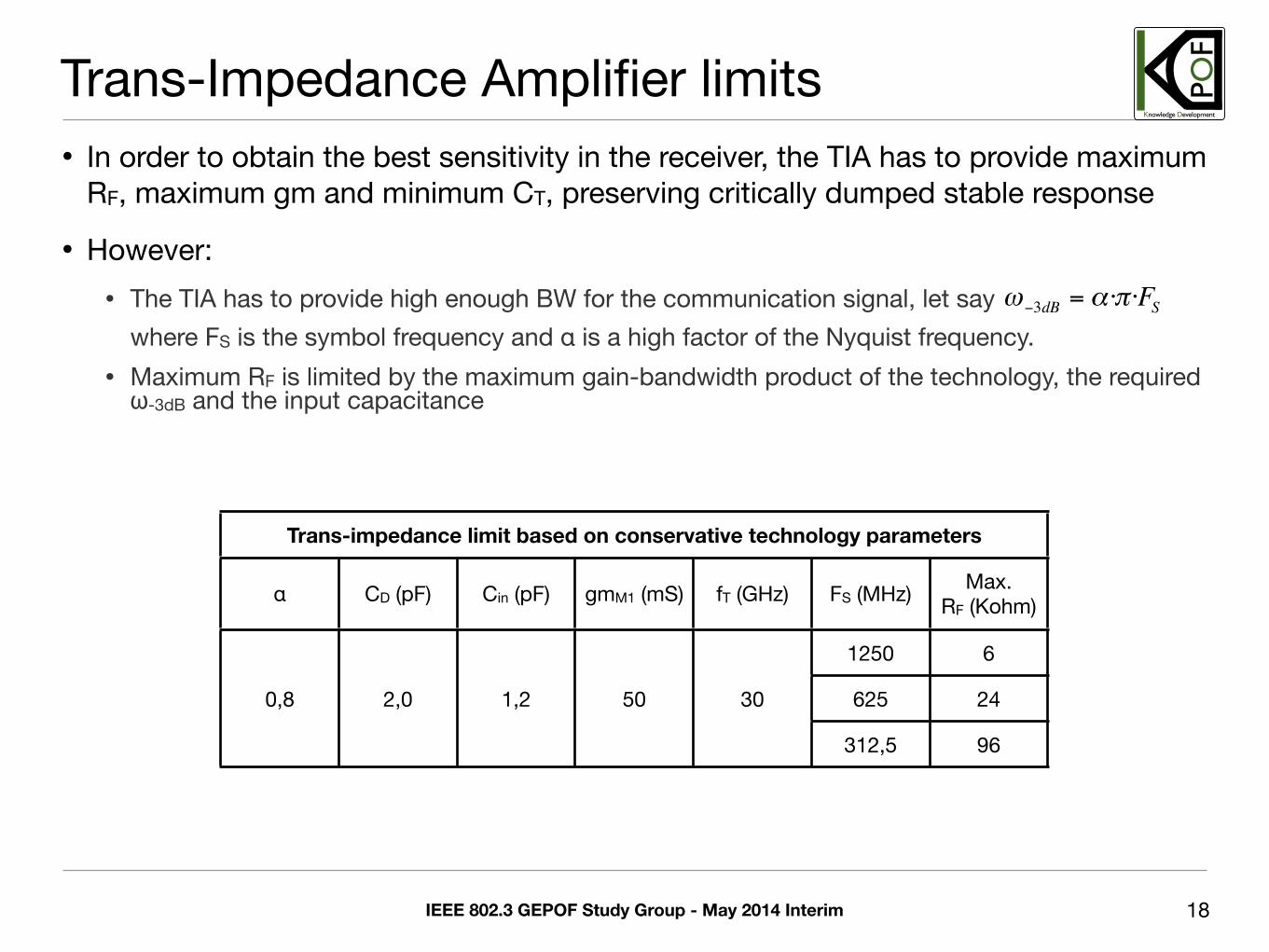
Trans-Impedance Amplifier limits• In order to obtain the best sensitivity in the receiver, the TIA has to provide maximum
RF, maximum gm and minimum CT, preserving critically dumped stable response
• However:• The TIA has to provide high enough BW for the communication signal, let say
where FS is the symbol frequency and α is a high factor of the Nyquist frequency.• Maximum RF is limited by the maximum gain-bandwidth product of the technology, the required
ω-3dB and the input capacitance
18
ω−3dB = α ·π ·FS
Trans-impedance limit based on conservative technology parametersTrans-impedance limit based on conservative technology parametersTrans-impedance limit based on conservative technology parametersTrans-impedance limit based on conservative technology parametersTrans-impedance limit based on conservative technology parametersTrans-impedance limit based on conservative technology parametersTrans-impedance limit based on conservative technology parameters
α CD (pF) Cin (pF) gmM1 (mS) fT (GHz) FS (MHz) Max.RF (Kohm)
0,8 2,0 1,2 50 30
1250 6
0,8 2,0 1,2 50 30 625 240,8 2,0 1,2 50 30
312,5 96
IEEE 802.3 GEPOF Study Group - May 2014 Interim
POF
Knowledge Development
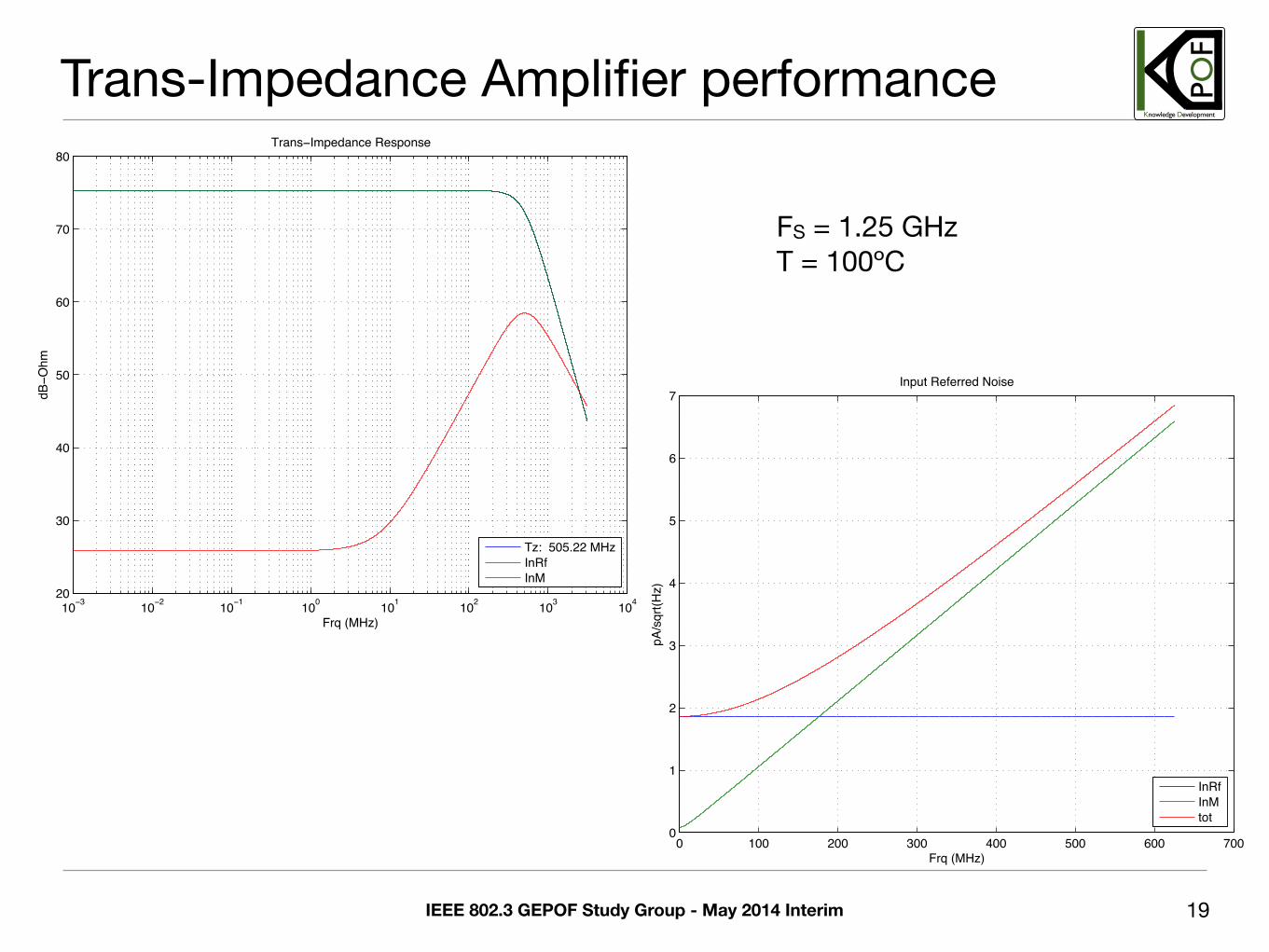
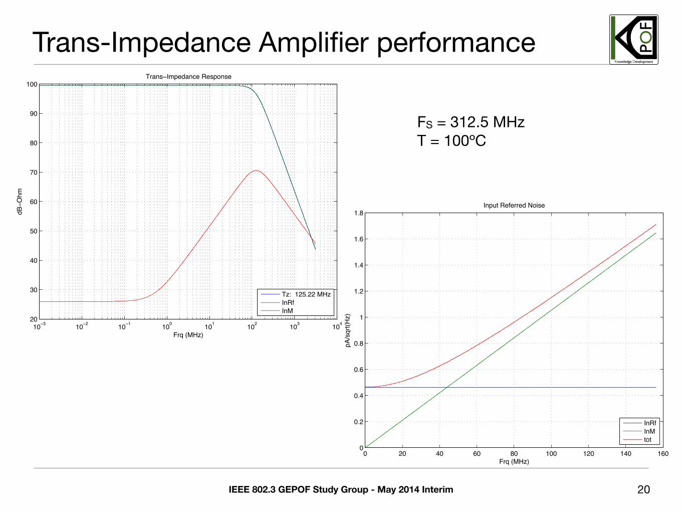
Trans-Impedance Amplifier performance
19
10−3 10−2 10−1 100 101 102 103 10420
30
40
50
60
70
80
Frq (MHz)
dB−O
hm
Trans−Impedance Response
Tz: 505.22 MHzInRfInM
0 100 200 300 400 500 600 7000
1
2
3
4
5
6
7
Frq (MHz)
pA/s
qrt(H
z)
Input Referred Noise
InRfInMtot
FS = 1.25 GHzT = 100ºC
IEEE 802.3 GEPOF Study Group - May 2014 Interim
POF
Knowledge Development
Trans-Impedance Amplifier performance
20
10−3 10−2 10−1 100 101 102 103 10420
30
40
50
60
70
80
90
100
Frq (MHz)
dB−O
hm
Trans−Impedance Response
Tz: 125.22 MHzInRfInM
0 20 40 60 80 100 120 140 1600
0.2
0.4
0.6
0.8
1
1.2
1.4
1.6
1.8
Frq (MHz)
pA/s
qrt(H
z)
Input Referred Noise
InRfInMtot
FS = 312.5 MHzT = 100ºC
IEEE 802.3 GEPOF Study Group - May 2014 Interim
POF
Knowledge Development
Conclusions• Main characteristics of the optical receiver have been provided in terms of
maximum achievable trans-impedance, bandwidth, and minimum achievable noise, considering limiting factors of Si-PIN and CMOS technologies.
• The results presented here will be used for Shannon’s capacity analysis in [perezaranda_02_0514_shannoncap]
21

IEEE 802.3 GEPOF Study Group - May 2014 Interim
POF
Knowledge Development
Questions?


