
Overcoming the ‘Memory Wall’
Abstract
Introduction
• How have 2d ram been changing
• Problem arising with need for more data, mem performance not increasing as fast as processor
performance
• What Intel and Micron have been doing
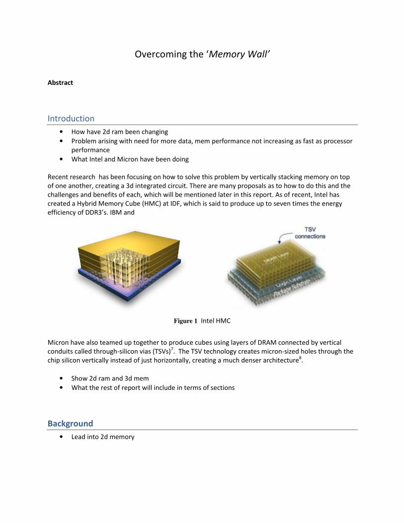
Recent research has been focusing on how to solve this problem by vertically stacking memory on top
of one another, creating a 3d integrated circuit. There are many proposals as to how to do this and the
challenges and benefits of each, which will be mentioned later in this report. As of recent, Intel has
created a Hybrid Memory Cube (HMC) at IDF, which is said to produce up to seven times the energy
efficiency of DDR3’s. IBM and
Figure 1 Intel HMC
Micron have also teamed up together to produce cubes using layers of DRAM connected by vertical
conduits called through-silicon vias (TSVs)7. The TSV technology creates micron-sized holes through the
chip silicon vertically instead of just horizontally, creating a much denser architecture8.
• Show 2d ram and 3d mem
• What the rest of report will include in terms of sections
Background
• Lead into 2d memory
DRAM
Dynamic random-access memory (DRAM) is a type of random-access memory that stores a bit of data
using a transistor and capacitor pair, which together make up the memory cell1,2
. The capacitor can be
either charged or discharged; these two states are represented by the two values of a bit, 0 and 1. The
transistor acts as a switch that lets the control circuitry on the chip read the capacitor's state of charge
or change it. Since capacitors leak charge, the information eventually fades unless the capacitor’s
charge is refreshed periodically, which is considered volatile, because their state is lost or reset when
power is removed from the system. Because of this refresh requirement, it is called dynamic memory.
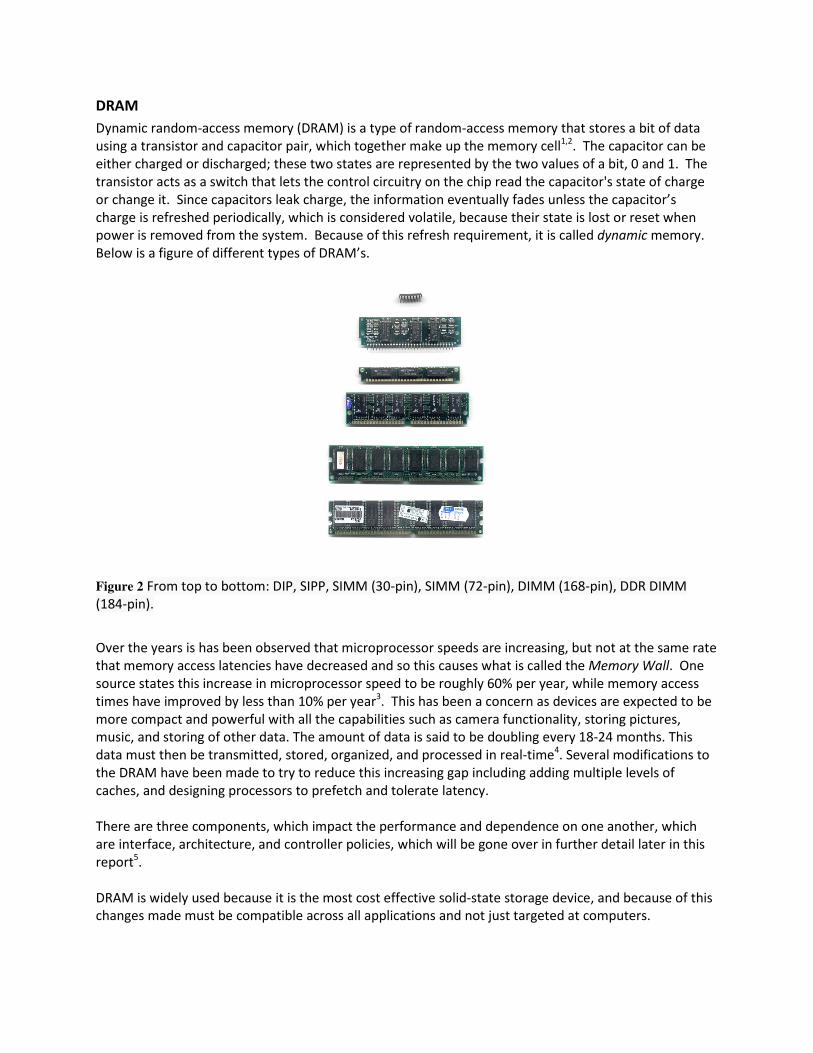
Below is a figure of different types of DRAM’s.
Figure 2 From top to bottom: DIP, SIPP, SIMM (30-pin), SIMM (72-pin), DIMM (168-pin), DDR DIMM
(184-pin).
Over the years is has been observed that microprocessor speeds are increasing, but not at the same rate
that memory access latencies have decreased and so this causes what is called the Memory Wall. One
source states this increase in microprocessor speed to be roughly 60% per year, while memory access
times have improved by less than 10% per year3. This has been a concern as devices are expected to be
more compact and powerful with all the capabilities such as camera functionality, storing pictures,
music, and storing of other data. The amount of data is said to be doubling every 18-24 months. This
data must then be transmitted, stored, organized, and processed in real-time4. Several modifications to
the DRAM have been made to try to reduce this increasing gap including adding multiple levels of
caches, and designing processors to prefetch and tolerate latency.
There are three components, which impact the performance and dependence on one another, which
are interface, architecture, and controller policies, which will be gone over in further detail later in this
report5.
DRAM is widely used because it is the most cost effective solid-state storage device, and because of this
changes made must be compatible across all applications and not just targeted at computers.

Main Memory Architecture
Traditional 3D-stacked implementations have used traditional 2D DRAM organizations, and simply
stacked them on top of a single-layer processor. While this does provide a significant benefit in the form
of reduced wire delay and power, it does not take full advantage of the many possibilities provided by a
3D organization.
To better describe why a 2D architecture is insufficient and to provide a basis for the architectural
changes that will be made in the 3D architectures, the specifics of 2D DRAM architecture will now be
discussed.
The general architecture for DRAM is an array of single-transistor bitcells accompanied by logic to access
those bits (refer to Error! Reference source not found.(a)).
Figure 3 (a) Organization of the memory hierarchy starting from L2 cache. (b) Details of one memory
rank, (c) Details of one memory bank6.
From left to right in the Error! Reference source not found.(a). above we see there is the L2 cache,
which holds copies of data from the most frequently used main memory. A cache reduces the average
latency a CPU would take to access memory. Then there is the miss status handling register, which keep
track of cache misses. The memory controller (MC), manages data going to and from memory by reading
and writing to it as well as controlling the refreshes.
When a miss occurs in the L2 cache, it requires accessing memory to satisfy this request. It must then
proceed to the MSHER to note this miss. The request is then forwarded to the memory controller to
access the memory. This request must wait in the memory request queue if there are other requests
made previous to it. A scheduler such as first in first out (FIFO) exists to determine which request to be
sent to memory first. When the request is ready, the MC forwards the physical address to be read or
written as well as manages the timing of other signals.
DRAM array are divided into ranks. For each DRAM there are about one or two ranks per module as
seen in Figure 3(b). Ranks are divided into banks, which consist of 2d arrays of bitcells. When a read
request is made, bits from the physical address are used to select the rank, bank, and row to read the
data from. It then takes the data from the row and latches it to the row buffer, which is then sent back
to the MC to send back to the processor. The row buffer allows for subsequent accesses to bypass the
array-read process. The data must eventually be written back to the bitcell array after any read and
contents within the array must be refreshed periodically since these contents are capable of leaking6.
Based on this generic process of a DRAM we can see that the primary area of concern in terms of speed
of memory requests are: 1) the number of clock cycles that elapse between a processor’s request for
data and the arrival of the first line of the requested data at the processor input pins (latency); and 2)

the rate at which the subsequent data lines are returned after the first line arrives (bandwidth)5. Figure
4 below illustrates this terminology.
Figure 4. Latency vs. Bandwidth Terminology. Latency is measure in time, typically nanoseconds.
Bandwidth is measure in data per time, typically Mbytes/Sec or GBytes/Sec. The first two Data packets
shown in the above figure are assumed to be from prior requests5.
Latency here is defined to be latency of a specific access or the average latency of all accesses in a given
workload.
Other factors to consider that affect the performance would be the number of memory accesses that
can be pipelined for a specific application, the frequency required for refreshing the dynamic cells, and if
a one or more banks are capable of being refreshed while one is being accessed.
Ways to leverage this latency would be to increase the number of ranks, banks, and rows per bank. The
more banks and ranks there are, the more you can run in parallel in terms of the number of
simultaneous open pages/rows that the memory system can support. Though more ranks require more
DRAM modules, and by increasing the number of banks requires more row decorders, sense amplifiers,
column muxes, and row buffers, which limits the area a bank can occupy. On the other hand, smaller
arrays could lower the latency because of the lower capacitance associated with the word and bit lines.
Though, it is stated that by either increasing or decreasing the size of the array increases the amount of
die area required per bit. Thus cost and performance increase together when ideally we would want
performance to increase while cost decreases. In addition, increasing the row buffer entries per bank
would increase the frequency of lower-latency row-buffer hits. One could also increase the width or
clock speed of buses, which would increase the bandwidth for transferring the data, but this is limited
by the pin counts on both ends of the components as well as area requirements on the motherboard for
the printed circuit board (PCB) traces.
The demand for DRAM’s are high due to the low cost of manufacturing it thus many are produced at a
time. In order to ensure for successful products, DRAM devices typically include some redundant bits in
the architecture in case a single cell or line fails. Thus when arrays are reduced in size, this would
increase the area penalty, which would mean that more redundant bits would be required, and
therefore the area required for these bits are increased. Device cost is inversely related to die area
exponentiated to a constant power. Thus any suggested solution which increases the area increases the
cost at a high rate, which might make this product too costly to buy.
Neither bandwidth can solve this memory wall problem. One of the reasons performance decreases is
due to the processor core waiting during the DRAM latency for critical data in order to proceed with the
execution. Again, increasing bandwidth by expanding bus width would increase the cost. One could
instead increase the bus speed instead to increase the bandwidth, but this would create high complexity
and higher power consumption.
3D stacked Memory
• Benefits in general of 3D memory over 2D
Architecture Changes Related to 3D-Stacked Memory
This section goes into detail regarding the specific architecture of a 3D-stacked memory system. It
describes the architecture of traditional systems to the extent that is necessary for an uninformed
reader to understand the importance of the newer 3D architectures. Then it delves further into the
proposed 3D architectures, at differing levels of granularity: from ranks to transistors.
In particular, this section discusses the changes to the main memory architecture, the cache
architecture, and processor architecture that a 3D-stacked system brings to light.
3D DRAM Architecture Changes
While the current 2D DRAM architecture is sufficient in a 2D system, there are a myriad of
improvements that may easily be made when considering a 3D-stacked memory architecture. This
section is a discussion of these improvements, their advantages and their limitations.
Increase Memory Bus Width
The first and easiest of these is simply increasing the memory bus width. In a 2D system, the memory
bus is severely limited by pin count and motherboard real estate. In a 3D system though, through-
silicon-vias (TSVs) make it possible to easily have thousands if not millions of connections between the
processor and main memory. Thus, increasing the memory bus to the maximum usable by the L2 cache,
the size of a cache line, is the first logical step. On most systems this is 64 bytes; this does not come
close to utilizing the potential bandwidth that is available in a 3D system.
A reasonable thought, therefore, is that the cache line size must be increased. The theoretical limit
without software changes is 4KB, a page. In a traditional 2D layout, such large cache lines are impractical
due to the number of cycles required to fetch the cache line. 3D-stacked memory removes this barrier
by providing a potential bandwidth high enough to fill a 4KB cache line in a single memory cycle. The
larger cache line would also reduce miss rate, given a large L2 cache and a moderate amount of spatial
locality in the application. However, it turns out that simply increasing the cache line size is not a valid
solution. Not only does a large cache line reduce L1 cache performance, the access time of the L2 cache
increases linearly with cache line size. This negates most of the benefits of a large cache line size, and
precludes its use.
<Possibly discuss cache structure and why cache access time scales linearly with cache line size>

Increase Memory Bus and Controller Frequency
Another necessary optimization for a 3D-stacked system is the increase in clock frequency for the
memory bus and the memory controller. In a 2D system, the memory controller doesn’t need to
schedule requests any faster than the DRAM can service them. Therefore, when the main memory
latency is drastically reduced by moving to a 3D-stacked memory system, the clock frequency of the
relevant memory units must be increased to compensate for the change.
This change does not provide great performance increase by itself; it is simply required in order to take
advantage of the lower memory access latencies.
Layer Separation and Optimization
Until this point, all of the improvements introduced by a 3D-stacked memory architecture are still
inherently 2-dimensional. However, it is possible to split functional blocks across multiple layers in a 3D
system. For example, a DRAM bank consisting of rows of bitcells and separate peripheral logic (row
decoder, sense amps, row buffer, and column select), can be split between two layers, separating the
memory from the logic.
A proposed architecture suggests four layers of DRAM memory and a layer of DRAM peripheral logic on
top of the processor. Ranks would be split across silicon layers, in order to reduce wire length and
capacitance. This is shown in Figure 5(b). This is compared to Figure 5(a), which shows traditional 2D
DRAM ranks stacked on top of a processor. The advantage obtained by separating the memory and logic
is that it provides the ability to optimize each layer for a separate purpose using different process
technologies. In this architecture, the layer of DRAM memory can be implemented in NMOS technology
optimized for density, while the logic layer can be implemented in CMOS technology optimized for
speed.
Optimizing particular silicon layers for a specific purpose can be very effective: splitting ranks across the
layers and using different optimization processes for particular layers improved memory access time by
32%, as Loh mentioned in his article, 3D-Stacked Memory Architectures for Multi-Core Processors.
Figure 5 DRAM stacked on top of a processor in a (a) traditional 2D DRAM rank setup, or (b) splitting
ranks across layers to isolate peripheral logic on a separate layer.
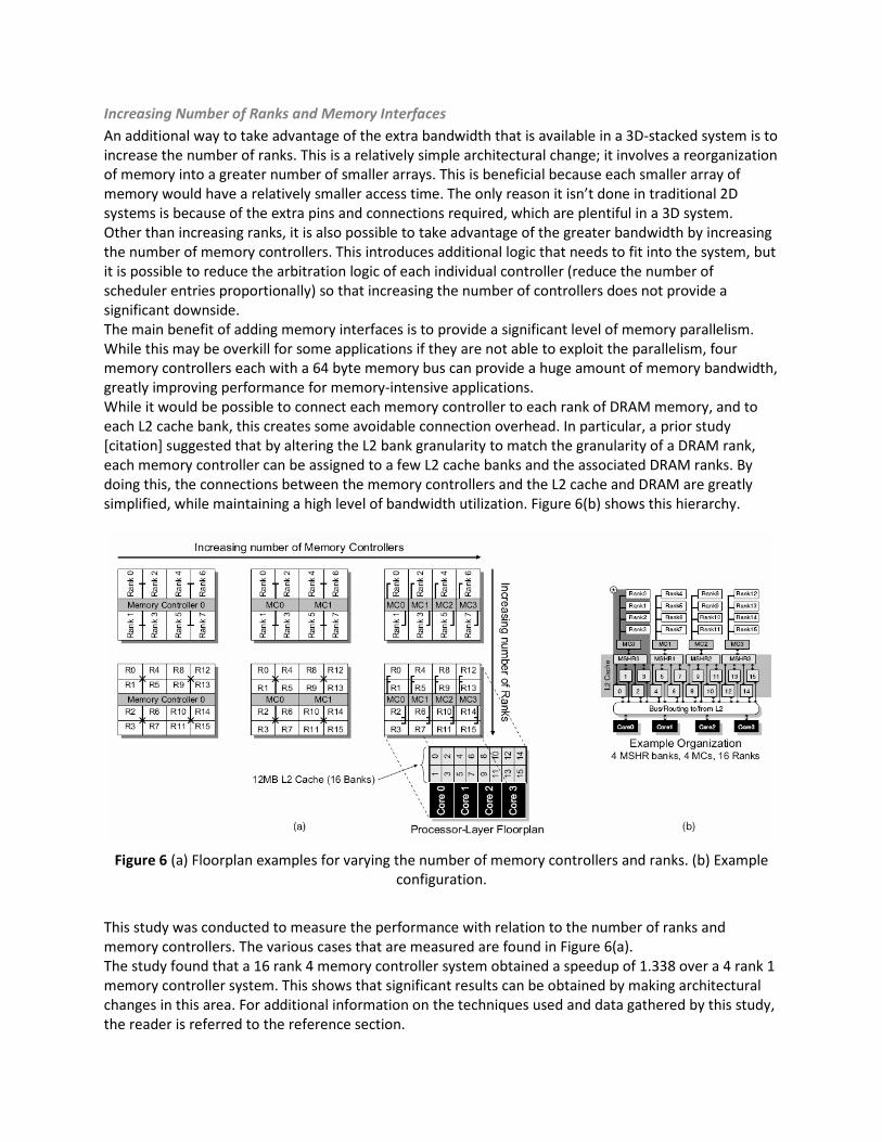
Increasing Number of Ranks and Memory Interfaces
An additional way to take advantage of the extra bandwidth that is available in a 3D-stacked system is to
increase the number of ranks. This is a relatively simple architectural change; it involves a reorganization
of memory into a greater number of smaller arrays. This is beneficial because each smaller array of
memory would have a relatively smaller access time. The only reason it isn’t done in traditional 2D
systems is because of the extra pins and connections required, which are plentiful in a 3D system.
Other than increasing ranks, it is also possible to take advantage of the greater bandwidth by increasing
the number of memory controllers. This introduces additional logic that needs to fit into the system, but
it is possible to reduce the arbitration logic of each individual controller (reduce the number of
scheduler entries proportionally) so that increasing the number of controllers does not provide a
significant downside.
The main benefit of adding memory interfaces is to provide a significant level of memory parallelism.
While this may be overkill for some applications if they are not able to exploit the parallelism, four
memory controllers each with a 64 byte memory bus can provide a huge amount of memory bandwidth,
greatly improving performance for memory-intensive applications.
While it would be possible to connect each memory controller to each rank of DRAM memory, and to
each L2 cache bank, this creates some avoidable connection overhead. In particular, a prior study
[citation] suggested that by altering the L2 bank granularity to match the granularity of a DRAM rank,
each memory controller can be assigned to a few L2 cache banks and the associated DRAM ranks. By
doing this, the connections between the memory controllers and the L2 cache and DRAM are greatly
simplified, while maintaining a high level of bandwidth utilization. Figure 6(b) shows this hierarchy.
Figure 6 (a) Floorplan examples for varying the number of memory controllers and ranks. (b) Example
configuration.
This study was conducted to measure the performance with relation to the number of ranks and
memory controllers. The various cases that are measured are found in Figure 6(a).
The study found that a 16 rank 4 memory controller system obtained a speedup of 1.338 over a 4 rank 1
memory controller system. This shows that significant results can be obtained by making architectural
changes in this area. For additional information on the techniques used and data gathered by this study,
the reader is referred to the reference section.
Increase DRAM Row Buffer Entries
<Increasing DRAM row buffer entries section>
Stacked Memory-Aware, Rich TSV-enabled 3D Memory Hierarchy
This section refers to a rather unique method of taking advantage of the high bandwidth available in a
3D system. The method is proposed in the paper [citation] and will henceforth be referred to as SMART-
3D (as it is in the original paper). While this section refers to a specific method and the implementation
of that method, concepts can be used in other areas, and it shows how redesigning architecture with
3D-stacked memory in mind can be beneficial.
Thermal Analysis
One of the biggest obstacles that a 3 dimensional memory/CPU structure must overcome is power
management and heat removal. Traditional 2D layouts have the benefit of being separate modules and
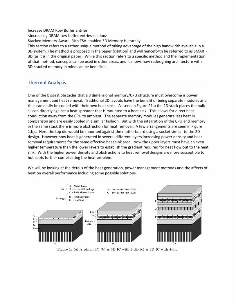
thus can easily be cooled with their own heat sinks. As seen in Figure P1.a the 2D stack places the bulk
silicon directly against a heat spreader that is mounted to a heat sink. This allows for direct heat
conduction away from the CPU to ambient. The separate memory modules generate less heat in
comparison and are easily cooled in a similar fashion. But with the integration of the CPU and memory
in the same stack there is more obstruction for heat removal. A few arrangements are seen in Figure
1.b,c. Here the top die would be mounted against the motherboard using a socket similar to the 2D
design. However now heat is generated in several different layers increasing power density and heat
removal requirements for the same effective heat sink area. Now the upper layers must have an even
higher temperature than the lower layers to establish the gradient required for heat flow out to the heat
sink. With the higher power density and obstructions to heat removal designs are more susceptible to
hot spots further complicating the heat problem.
We will be looking at the details of the heat generation, power management methods and the affects of
heat on overall performance including some possible solutions.
Heat Generation
There are advantages with regard to power requirements of a 3D design due to the fact that
interconnecting wires are shortened. The reduction of interconnecting wires can have a significant
impact in power consumption [P4.5] This is because the shorter wires do not require as large of a driver
and carry a lower power signal over a smaller distance with less electrical resistance. However stacking
the CPU and memory dies comes at the cost of higher power density of the heat generating parts being
in closer proximity to each other. The higher power density combined with greater path for heat
dissipation raises on-chip temperatures. It has been estimated that stacking dies as seen in Figure P1
will17°C result in a 17°C rise in max temperature between the planar 2D (Fig P1.a) and 2 layer
implementation of Figure P1.b. In comparison the 4 layer model (Fig P1.c) saw a 33°C increase in max
temperature compared to the 2D design of the Alpha 21394 processor-memory structure in a 70nm
process with a supply of 0.9 volts. [P4]
Performance Affects
There have been countless testing and simulations done to evaluate the performance
improvements with 3D memory structures. Since simulation of the heat problem is difficult few of
studies have accurately considered heat's affects on system performance.
In an analysis completed at the University of California [P1] these thermal effects were
considered when comparing performance of 2D vs. 3D structures. It was pointed out that previous
studies had under estimated the negative affects of heat on system performance because small scale
processes had not been evaluated. This study simulated 120nm process where leakage power is highly
temperature sensitive since with an exponential relationship. Similar 2D and 3D structures were stacked
up against each other where cache and memory designs were assumed to be identical. The 3D design
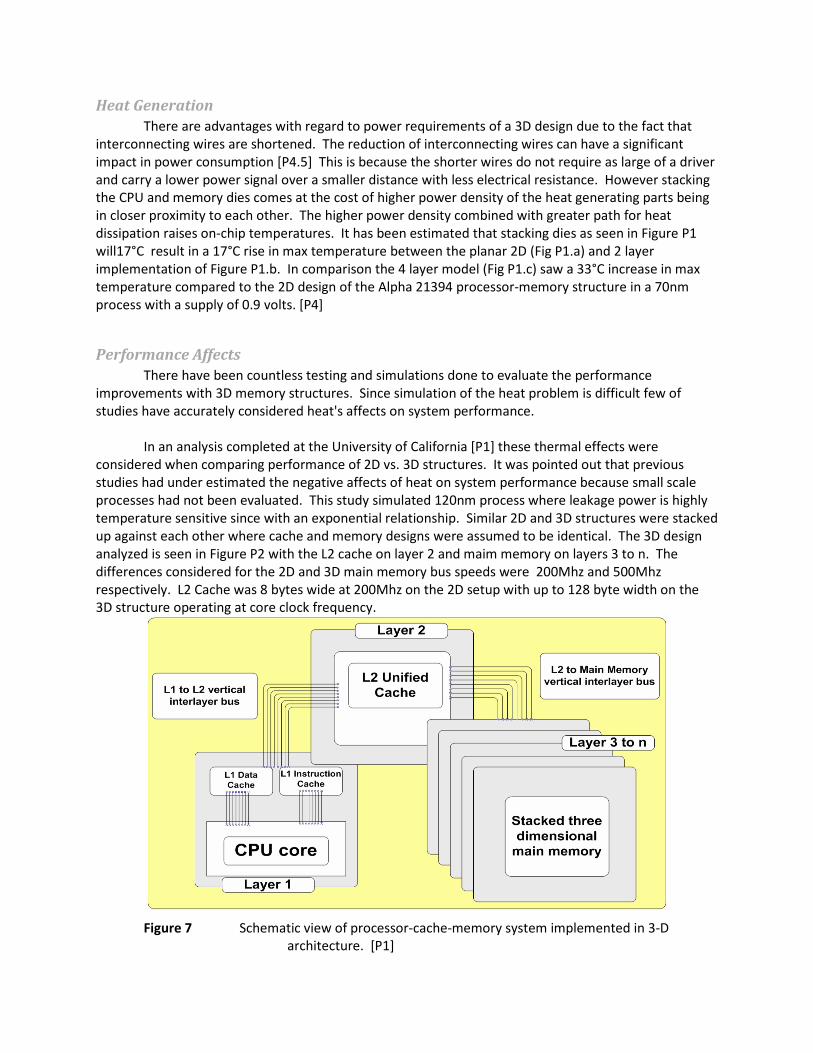
analyzed is seen in Figure P2 with the L2 cache on layer 2 and maim memory on layers 3 to n. The
differences considered for the 2D and 3D main memory bus speeds were 200Mhz and 500Mhz
respectively. L2 Cache was 8 bytes wide at 200Mhz on the 2D setup with up to 128 byte width on the
3D structure operating at core clock frequency.
Figure 7 Schematic view of processor-cache-memory system implemented in 3-D
architecture. [P1]

Figure 8 Performance comparison with frequency adjustments based on operating temperature.

1 Introduction
The continuation of Moore’s law by conventional CMOS scaling is becoming more and more challenging,
requiring huge capital investments. 3D Packaging with 3D TSV interconnects provides another path
towards the “More than Moore”, with relatively smaller capital investments. As current scaling trends
require enormous investments only affordable to a select few, Moore’s Law reaches its limit and three
dimensional integration becomes inevitable. 3D IC solution is the natural evolution for the IC industry; it
is the convergence of performance, power and portability. The economic and technical improvements in
performance, power, form factor, time-to-market and cost will drive the use of 3D systems going
forward. 3D ICs with TSV are being widely developed around the world for two
reasons. First of all, heterogeneous integration of logic, memory, graphics, power and sensor ICs
requires it since these functionalities cannot be integrated into a single chip. Secondly, 3D ICs with TSVs
offer improved electrical performance due to the short interconnect and ultra-high number of TSV
interconnections between stacked ICs to address the perceived engineering limits in leakage and
electrical performance of CMOS ICs beyond 11-16nm. The 3D TSV IC's have superior advantages over
the alternative package choices. By combining the performance and power of system-on-chip (SOC) with
the functionality and time-to-market advantages of system-in-package (SiP), TSV offers the best of both
for achieving very high densities for memory and logic.
Figure 8 SEMATECH's 3D IC research program shows a comparison between 3D TSV and alternatives.
Benefits
In this survey the focus is exclusively on 3D memories. It promises a better solution to problems
that are encountered as feature sizes reduce to below 65 nm.
As processors become faster, latency differences between the processor and memory access is
increasing even more day by day. This brings in the need for faster memories. Also, many processor
architectures now have 3 levels of cache on-chip and the energy consumption for offchip memory
access is considerably high. The problem with having memory on the same die as the user logic is that it
has to be compatible with the user logic (in the same technology). This is inefficient, as many a times,
user logic is designed in a smaller feature size than the memory. Also, having so many memories
increases the die footprint. By going 3D, we alleviate these issues. The logic and memory can be on
separate wafers, thereby reducing complexity and number of process steps. They can be individually
processed in different feature sizes or even on heterogenous materials. Chip to wafer bonding even
allows stacking together chips of different sizes with the base die being the largest.
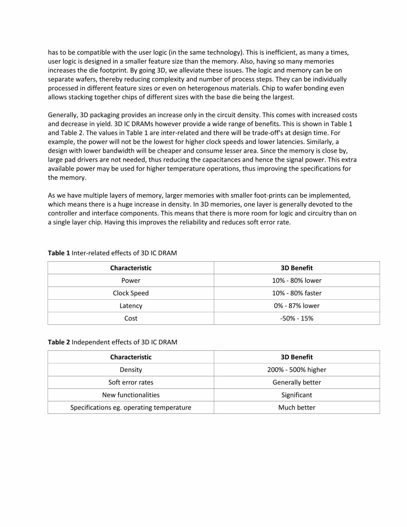
Generally, 3D packaging provides an increase only in the circuit density. This comes with increased costs
and decrease in yield. 3D IC DRAMs however provide a wide range of benefits. This is shown in Table 1
and Table 2. The values in Table 1 are inter-related and there will be trade-off's at design time. For
example, the power will not be the lowest for higher clock speeds and lower latencies. Similarly, a
design with lower bandwidth will be cheaper and consume lesser area. Since the memory is close by,
large pad drivers are not needed, thus reducing the capacitances and hence the signal power. This extra
available power may be used for higher temperature operations, thus improving the specifications for
the memory.
As we have multiple layers of memory, larger memories with smaller foot-prints can be implemented,
which means there is a huge increase in density. In 3D memories, one layer is generally devoted to the
controller and interface components. This means that there is more room for logic and circuitry than on
a single layer chip. Having this improves the reliability and reduces soft error rate.
Table 1 Inter-related effects of 3D IC DRAM
Characteristic 3D Benefit
Power 10% - 80% lower
Clock Speed 10% - 80% faster
Latency 0% - 87% lower
Cost -50% - 15%
Table 2 Independent effects of 3D IC DRAM
Characteristic 3D Benefit
Density 200% - 500% higher
Soft error rates Generally better
New functionalities Significant
Specifications eg. operating temperature Much better

Manufacturing Challenges
Costs vs. Performance
Benefits & Applications
Conclusion
References
DRAM
1. http://en.wikipedia.org/wiki/Random-access_memory
2. http://en.wikipedia.org/wiki/Dynamic_RAM
Dynamic random-access memory (DRAM)
3. Bridging the processor memory gap
4. Platform 2015: Intel® Processor and Platform Evolution for the Next Decade
5. Dram.pdf
6. 3D stacked memory architecture for multi-core processors
Benefirs
1. http://repository.lib.ncsu.edu/ir/bitstream/1840.16/6346/1/etd.pdf
2. http://www.monolithic3d.com/2/post/2011/06/introducing-our-monolithic-3d-dram-
technology.html
3. G. Loi, B. Agrawal, N. Srivastava, S. Lin, T. Sherwood, and K. Banerjee, “A Thermally-Aware
Performance Analysis of Vertically Integrated (3-D) Processor-Memory Hierarchy,” in Design
Automation Conference, 2006, pp. 991-996.


