

Power supply: AC220-240 V, 50 Hz
Power consumption: 13 W +/-1,3W
standby mode: 2W+/-0,4W
Dimensions: 430 (W)×260 (D)×60 (H) mm
(excluding protrusions)
Mass: 2.2 kg
Signal system: PAL625/50, PAL525/60, NTSC
Operating temperature range: +5 to +35°C
Operating humidity range: 5 to 90% RH (no condensation)
Region number: Region No.2
Playable disctype:(1) DVD-Video, DVD-RAM, DVD-Audio, DVD-R (R4.7)
(2) CD-Audio (CD-DA) (3) Video CD
(4) CD-R/CD-RW (CD-DA, Video CD formatted discs)
(5) MP3 (audio), WMA (audio), JPG (picture)
Maximum number of tracks and groups recognizable:
999 tracks and 99 groups
Compatible compression rate: between 32 kbps and 320 kbps
Video output:Output level: 1 Vp-p (75Ω)
Output terminal: Pin jack/ AV
Number of terminals: 1 system
S video output:Y output level: 1 Vp-p (75Ω)
C output level: NTSC: 0.286 Vp-p (75Ω)
PAL: 0.300 Vp-p (75Ω)
Output terminal: S terminal/AV
Number of terminals: 1 system
© 2003 Matsushita Electric Industrial CO., Ltd. Allrights reserved. Unauthorized copying anddistribution is a violation of law.
DVD-S35EDVD-S35EBDVD-S35EGDVD-S31EGColour(S).......................Silver Type(K).......................Black Type
RGB video output:R output level: 0.7 Vp-p (75Ω) +/-10%
G output lebel: 0.7 Vp-p (75Ω) +/-10%
B output level 0.7 Vp-p (75Ω) +/-10%
Output terminal: AV
Number of terminals: 1 system
Audio output:Output level: 2 Vrms (1 kHz, 0 dB)
Output terminal: Pin jack/ AV
Number of terminals: 2CH 1system
Audio performance:(1) Frequency response: DVD (linear audio):
4 Hz-22 kHz (48 kHz sampling)
4 Hz-44 kHz (96 kHz sampling)
CD audio: 4 Hz-20 kHz
(2) S/N ratio: CD audio: 115 dB
(3) Dynamic range: DVD (linear audio): 97 dB
CD audio: 97 dB
(4) Total harmonic distortion: CD audio: 0.0025%
Digital audio output:Optical digital output: Optical terminal
Pickup:Wave length: 658 nm/790 nm
Laser power: CLASS 2/CLASS 1
Note:Specifications are subject to change without notice.
Mass and dimensions are approximate.
DVD Player
Specifications
ORDER NO: MAD0303001C2

1 SAFETY PRECAUTIONS 3 1.1. GENERAL GUIDELINES 3
2 PREVENTION OF ELECTRO STATIC DISCHARGE (ESD) TOELECTROSTATICALLY SENSITIVE (ES) DEVICES 4
3 Precaution of Laser Diode 5 3.1. About lead free solder (PbF) 5
4 General Description 6 4.1. Operating instructions 6
5 PREVENTION OF STATIC ELECTRICITY DISCHARGE 7 5.1. Grounding for electrostatic breakdown prevention 7
5.2. Handling Precautions for Traverse Unit (Optical Pickup) 7
6 Disassembling the Casing and Checking PCBs 8 6.1. Dissasembly Procedure 8
6.2. Casing Parts and PCB Positions 8
6.3. Top Cover 9
6.4. Tray 9
6.5. Front Panel Unit 10
6.6. Rear Panel 10
6.7. Power PCB Unit 10
6.8. Decoder PCB 11
6.9. Mechanism Unit 11
6.10. Terminal PCB 11
6.11. Front Panel PCB Unit 11
6.12. Servicing Position 12
7 OPTICAL PICKUP SELF-DIAGNOSIS AND REPLACEMENTPROCEDURE 13 7.1. Self-diagnosis 13
7.2. Cautions to be used before replacing the Optical Pickup
Unit and Spindle Motor assembly 14
8 Self-Diagnosis Function and Service Modes 15 8.1. Service Mode Table 1 15
8.2. DVD Self Diagnostic Function-Error Code 15
8.3. Last Error Code saved during NO PLAY 16
8.4. Service mode table 2 17
8.5. Overview of each function 19
8.6. Sales demonstration lock function 19
8.7. Handling After Completing Repairs 19
8.8. Service Precautions 20
9 ASSEMBLING AND DISASSEMBLING THE MECHANISM UNIT 21 9.1. Disassembly Procedure 21
9.2. Terminal PCB 21
9.3. Clamp Plate Unit 21
9.4. Tray 22
9.5. FG PCB Unit 23
9.6. Traverse Block 23
9.7. Traverse Gear 24
9.8. Optical Pickup Unit 24
9.9. Disassembling the Middle Chassis 29
9.10. Disassembling the Traverse Gear A 29
9.11. Disassembling the Spindle Motor Unit 29
10 ADJUSTMENT PROCEDURES 30 10.1. Service Tools and Equipment 30
10.2. Important points in adjustment 30
10.3. Storing and Handling Test Discs 30
10.4. Optical adjustment 31
11 Abbreviations 32 12 Voltage Chart 34 13 BLOCK DIAGRAM 37
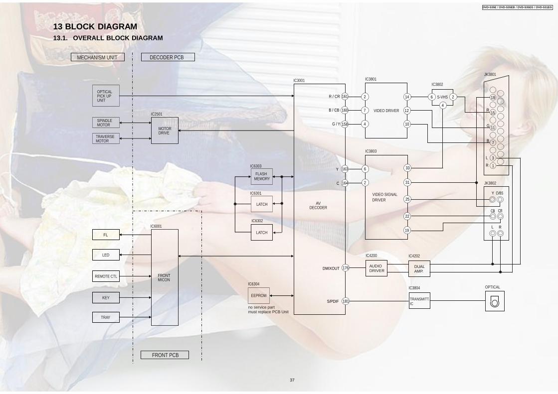
13.1. OVERALL BLOCK DIAGRAM 37
13.2. POWER BLOCK DIAGRAM 38
13.3. FRONT PANEL BLOCK DIAGRAM 39
13.4. SERVO BLOCK DIAGRAM (Decoder PCB) 40
14 SCHEMATIC DIAGRAM 41 14.1. INTERCONNECTION SCHEMATIC DIAGRAM 41
14.2. POWER PCB UNIT 42
14.3. FRONT PANEL PCB UNIT 43
14.4. DECODER INTERCONNECTION 44
14.5. DECODER PCB (AV DECODER) 45
14.6. DECODER DRIVE CONNECTION 46
14.7. DECODER FLASH MEMORY 47
14.8. DECODER AV INTERFACE 48
14.9. DECODER AUDIO DAC 49
14.10. TERMINAL PCB 50
15 PRINT CIRCUIT BOARD 51 15.1. Decoder PCB Unit 51
15.2. Power PCB Unit 52
15.3. TERMINAL PCB 53
15.4. Front PCB Unit 54
16 EXPLODED VIEWS 55 16.1. Casing Parts& Mechanism Section Exploded View 55
16.2. Mechanism Section Exploded View 56
16.3. Packing& Accessories Section Exploded View 57
17 REPLACEMENT PARTS LIST 58 18 All Schematic Diagram for printing with A4 64
CONTENTS Page Page
2
DVD-S35E / DVD-S35EB / DVD-S35EG / DVD-S31EG

1.1.1. LEAKAGE CURRENT COLDCHECK
1. Unplug the AC cord and connect a jumper between the twoprongs on the plug.
2. Measure the resistance value, with an ohmmeter, betweenthe jumpered AC plug and each exposed metallic cabinetpart on the equipment such as screwheads, connectors,control shafts, etc. When the exposed metallic part has areturn path to the chassis, the reading should be between1MΩ and 5.2MΩ.When the exposed metal does not have a return path to
the chassis, the reading must be .
Figure 1
1.1.2. LEAKAGE CURRENT HOT CHECK(See Figure 1)
1. Plug the AC cord directly into the AC outlet. Do not use anisolation transformer for this check.
2. Connect a 1.5kΩ, 10 watts resistor, in parallel with a 0.15µFcapacitor, between each exposed metallic part on the setand a good earth ground such as a water pipe, as shown inFigure 1.
3. Use an AC voltmeter, with 1000 ohms/volt or moresensitivity, to measure the potential across the resistor.
4. Check each exposed metallic part, and measure thevoltage at each point.
5. Reverse the AC plug in the AC outlet and repeat each of theabove measurements.
6. The potential at any point should not exceed 0.75 voltsRMS. A leakage current tester (Simpson Model 229 orequivalent) may be used to make the hot checks, leakagecurrent must not exceed 1/2 milliamp. In case ameasurement is outside of the limits specified, there is apossibility of a shock hazard, and the equipment should berepaired and rechecked before it is returned to thecustomer.
1 SAFETY PRECAUTIONS1.1. GENERAL GUIDELINES 1. When servicing, observe the original lead dress. If a short circuit is found, replace all parts which have been overheated or
damaged by the short circuit. 2. After servicing, see to it that all the protective devices such as insulation barriers, insulation papers shields are properly
installed. 3. After servicing, make the following leakage current checks to prevent the customer from being exposed to shock hazards.
3
DVD-S35E / DVD-S35EB / DVD-S35EG / DVD-S31EG
2 PREVENTION OF ELECTRO STATIC DISCHARGE (ESD)TO ELECTROSTATICALLY SENSITIVE (ES) DEVICES
Some semiconductor (solid state) devices can be damaged easily by static electricity. Such components commonly are calledElectrostatically Sensitive (ES) Devices. Examples of typical ES devices are integrated circuits and some field-effect transistors andsemiconductor "chip" components. The following techniques should be used to help reduce the incidence of component damagecaused by electro static discharge (ESD). 1. Immediately before handling any semiconductor component or semiconductor-equipped assembly, drain off any ESD on your
body by touching a known earth ground. Alternatively, obtain and wear a commercially available discharging ESD wrist strap,which should be removed for potential shock reasons prior to applying power to the unit under test.
2. After removing an electrical assembly equipped with ES devices, place the assembly on a conductive surface such as alminumfoil, to prevent electrostatic charge buildup or exposure of the assembly.
3. Use only a grounded-tip soldering iron to solder or unsolder ES devices. 4. Use only an anti-static solder removal device. Some solder removal devices not classified as "anti-static (ESD protected)" can
generate electrical charge sufficient to damage ES devices. 5. Do not use freon-propelled chemicals. These can generate electrical charges sufficient to damage ES devices. 6. Do not remove a replacement ES device from its protective package until immediately before you are ready to install it. (Most
replacement ES devices are packaged with leads electrically shorted together by conductive foam, aluminium foil orcomparable conductive material).
7. Immediately before removing the protective material from the leads of a replacement ES device, touch the protective materialto the chassis or circuit assembly into which the device will be installed.Caution
Be sure no power is applied to the chassis or circuit, and observe all other safety precautions. 8. Minimize bodily motions when handling unpackaged replacement ES devices. (Otherwise harmless motion such as the
brushing together of your clothes fabric or the lifting of your foot from a carpeted floor can generate static electricity (ESD)sufficient to damage an ES device).
4
DVD-S35E / DVD-S35EB / DVD-S35EG / DVD-S31EG
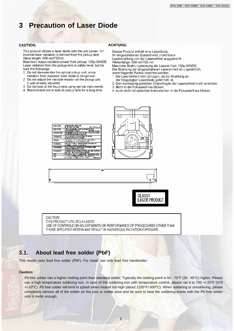
3 Precaution of Laser Diode
3.1. About lead free solder (PbF)This model uses lead free solder (PbF). For repair use only lead free handsolder.
Caution:Pb free solder has a higher melting point than standard solder; Typically the melting point is 50 - 70°F (30 - 40°C) higher. Pleaseuse a high temperature soldering iron. In case of the soldering iron with temperature control, please set it to 700 +/-20°F (370+/-10°C). Pb free solder will tend to splash when heated too high (about 1100°F/ 600°C). When soldering or unsoldering, pleasecompletely remove all of the solder on the pins or solder area and be sure to heat the soldering points with the Pb free solderuntil it melts enough.
5
DVD-S35E / DVD-S35EB / DVD-S35EG / DVD-S31EG

4 General Description4.1. Operating instructions
ENTER
1 2 3
4 5
7 8 9
0
6
DVD PLAYER
N2QAJB000069
A.SRD
CINEMA
D.ENH
GROUP CANCEL
10
SUBTITLE AUDIO ANGLE/PAGE QUICK REPLAY
PLAY MODE ZOOM REPEATPOSITIONMEMORY
DISPLAY RETURN
MENU
PLAY LISTDIRECT NAVIGATOR
TOPMENU
SLEEP SETUP OPEN/CLOSE
S IPK /SLO ARW SE CH
STOPPAUSE PLAY
ENTER to accept the menu function you selected
Cursor keys
The remote control unit
Switches on and off the DVD player from stand-by mode
SLEEP Switches off the unit at the set time
SETUP Displays the DVD player menus
OPEN/CLOSE Opens and closes the disc tray
A.SRD ADVANCED SURROUND: Provides something similar to a surround effect
CINEMA Enhances the contrast of dark scenes
D.ENH DIALOGUE ENHANCER: Puts up the volume of the dialogue tone
GROUP Displays on-screen any groups of MP3 tracks
CANCEL Undoes entries or selections
0...9
Numeric key pad; press 0 to input two-digit numbers
SKIP
Press to skip chapters or CD tracks
SLOW/SEARCH
Slow motion and search function
STOP
Press to stop playback
PAUSE
Press to pause playback
PLAY
Press to start playback
DIRECT NAVIGATOR/
TOP MENU Displays the main menu of a DVD, RAM disc or MP3
PLAY LIST/MENU Displays the menu screen of a DVD or the MP3 menu
DISPLAY Enables the on-screen display
RETURN Hides the menu and resumes playback
SUBTITLE Selects the language of subtitles during playback
AUDIO Changes the sound track language during playback
ANGLE/PAGE Chooses from various camera angles during playback
QUICK REPLAY Repeats the last 7 seconds of a film
PLAY MODE Programme memory
ZOOM ZOOM function during playback
REPEAT REPEAT function
POSITION MEMORY Resumes playback at stored position following an interruption
6
DVD-S35E / DVD-S35EB / DVD-S35EG / DVD-S31EG
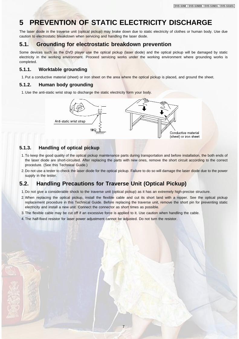
5 PREVENTION OF STATIC ELECTRICITY DISCHARGEThe laser diode in the traverse unit (optical pickup) may brake down due to static electricity of clothes or human body. Use duecaution to electrostatic breakdown when servicing and handling the laser diode.
5.1. Grounding for electrostatic breakdown preventionSome devices such as the DVD player use the optical pickup (laser diode) and the optical pickup will be damaged by staticelectricity in the working environment. Proceed servicing works under the working environment where grounding works iscompleted.
5.1.1. Worktable grounding 1. Put a conductive material (sheet) or iron sheet on the area where the optical pickup is placed, and ground the sheet.
5.1.2. Human body grounding 1. Use the anti-static wrist strap to discharge the static electricity form your body.
5.1.3. Handling of optical pickup 1. To keep the good quality of the optical pickup maintenance parts during transportation and before installation, the both ends of
the laser diode are short-circuited. After replacing the parts with new ones, remove the short circuit according to the correctprocedure. (See this Technical Guide.)
2. Do not use a tester to check the laser diode for the optical pickup. Failure to do so will damage the laser diode due to the powersupply in the tester.
5.2. Handling Precautions for Traverse Unit (Optical Pickup) 1. Do not give a considerable shock to the traverse unit (optical pickup) as it has an extremely high-precise structure. 2. When replacing the optical pickup, install the flexible cable and cut its short land with a nipper. See the optical pickup
replacement procedure in this Technical Guide. Before replacing the traverse unit, remove the short pin for preventing staticelectricity and install a new unit. Connect the connector as short times as possible.
3. The flexible cable may be cut off if an excessive force is applied to it. Use caution when handling the cable. 4. The half-fixed resistor for laser power adjustment cannot be adjusted. Do not turn the resistor.
7
DVD-S35E / DVD-S35EB / DVD-S35EG / DVD-S31EG
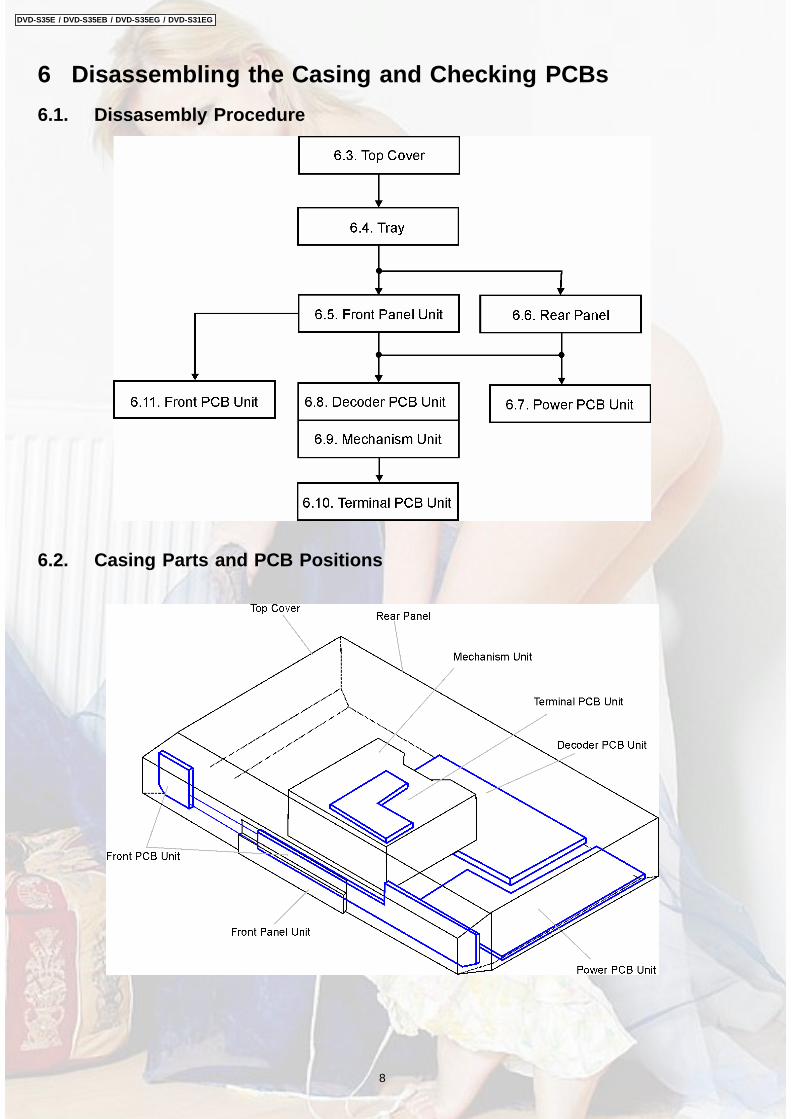
6 Disassembling the Casing and Checking PCBs6.1. Dissasembly Procedure
6.2. Casing Parts and PCB Positions
8
DVD-S35E / DVD-S35EB / DVD-S35EG / DVD-S31EG

6.4. Tray 1. Pull the tray out of the mechanism unit. Remove the gear
and install it onto a screwdriver to make a gear jig. 2. Insert the gear jig into the tray open/close hole. 3. Turn the gear jig counterclockwise to open the tray. 4. Remove the tray dressing from the tray section.
6.3. Top Cover 1. Unscrew the screws.
9
DVD-S35E / DVD-S35EB / DVD-S35EG / DVD-S31EG

6.5. Front Panel Unit 1. Remove the screws.
2. Release the tabs. 3. Release the connector (inside).
6.6. Rear Panel 1. Unscrew the screws 2. Release the tabs.
6.7. Power PCB Unit 1. Unscrew the screws. 2. Remove the connectors. 3. Pull out the Power PCB Unit vertically.
10
DVD-S35E / DVD-S35EB / DVD-S35EG / DVD-S31EG

6.8. Decoder PCB 1. Unscrew the screws. 2. Pull out the Mechanism Unit together with the Decoder PCB
Unit. 3. Unscrew the Screw bottom side of the Decoder PCB Unit.
6.9. Mechanism Unit 1. Remove the connectors between
Mechanism Unit and Decoder PCB Unit.
6.10. Terminal PCB 1. Unscrew the screw. 2. Remove the solders. 3. Remove the connector.
6.11. Front Panel PCB Unit 1. Unscrew the screws. 2. Remove the Chassis Ornament. 3. Remove the Front PCB Unit.
11
DVD-S35E / DVD-S35EB / DVD-S35EG / DVD-S31EG
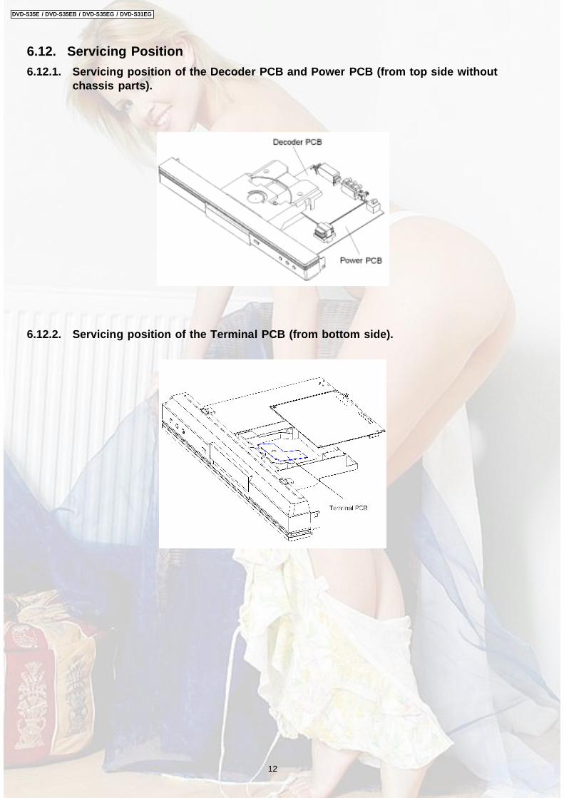
6.12. Servicing Position6.12.1. Servicing position of the Decoder PCB and Power PCB (from top side without
chassis parts).
6.12.2. Servicing position of the Terminal PCB (from bottom side).
12
DVD-S35E / DVD-S35EB / DVD-S35EG / DVD-S31EG

7 OPTICAL PICKUP SELF-DIAGNOSIS ANDREPLACEMENT PROCEDURE
7.1. Self-diagnosisThe optical pickup self-diagnosis function and tilt adjustment check function have been included in this unit. When repairing, usethe following procedure for effective Self-diagnosis and tilt adjustment. Be sure to use the self-diagnosis function before replacingthe optical pickup when "NO DISC" is displayed. As a guideline, you should replace the optical pickup when the value of the laserdrive current is more than 55.Note:
Press the power button to turn on the power, and check the value within three minutes before the unit warms up. (Otherwise,the result will be incorrect.)
13
DVD-S35E / DVD-S35EB / DVD-S35EG / DVD-S31EG

Cautions to be taken when replacing the optical pickupThe optical pickup may break down due to the staticelectricity of human body. Take proper protection measuresagainst static electricity before repairing the parts aroundthe optical pickup. (See the page describing thePREVENTION OF STATIC ELECTRICITYDISCHARGE.) 1. Do not touch the areas around the laser diode and
actuator. 2. Do not judge the laser diode with a tester. (The tester
will be damaged easily.) 3. It is recommended to use a destaticized soldering iron
for short-circuiting or removing the laser diode.
(Recommended soldering iron) HAKKO ESD Product 4. Solder the land of the flexible cable in the optical pickup.
Note: • • • • When using a soldering iron which is not
destaticized, short-circuit the terminal face of theflexible case with a clip. After that, short-circuitthe land.
• • • • After the repairing work is completed, remove thesolder according to the correct procedure shownin this Technical Guide.
7.2. Cautions to be used before replacing the Optical Pickup Unit andSpindle Motor assembly
Before replacing the optical pickup unit and spindle motor assembly, check the total using hours for each of them. The checkingmethod is as follows:
14
DVD-S35E / DVD-S35EB / DVD-S35EG / DVD-S31EG
8 Self-Diagnosis Function and Service Modes8.1. Service Mode Table 1The service modes can be activated by pressing various button combination on the player and remote control unit.
Player buttons Remote control unit buttons Application NotePAUSE
+OPEN/CLOSE
0 Displaying the UHF display F_ _ _ Refer to section 8.2. Self-Diagnosis Function (UHFDisplay).
5 Jitter check, tilt adjustment*Display shows J_xxx_yyy_zz"yyy" and "zz" shown to the right have nothing to do with the jittervalue. "yyy" is the error counter, while "zz" is the focusdrivevalue.Refer to section 10.4. for Optical Pickup Tilt AdjustmentProcedure.
Refer to section 10.4.Optical Pickup TiltAdjustment
6 Checking the region numbers and broadcast system7 Checking the program version9 Lighting Confirmation Function of Display Tube
DISPLAY Checking the laser drive current Refer to section 9Optical PickupReplacement Procedure.
PAUSE Writing the laser drive current value after replacing the opticalpickup (do not use for anything other than optical pickupreplacement)
PAUSESKIP/SEARCH<<
OPEN/CLOSE
Initializing the DVD player(restoring factory preset settings)
Refer to section 8.4.Initializing the DVDplayer.
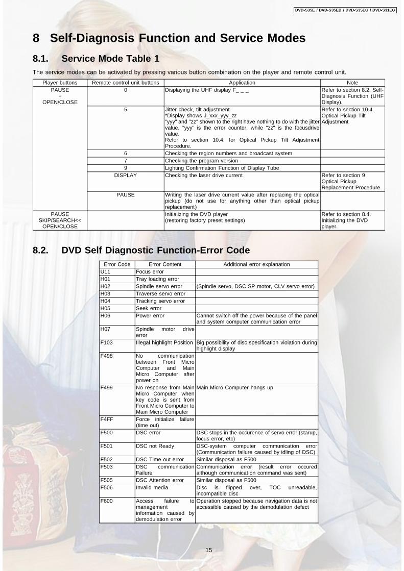
8.2. DVD Self Diagnostic Function-Error CodeError Code Error Content Additional error explanation
U11 Focus errorH01 Tray loading errorH02 Spindle servo error (Spindle servo, DSC SP motor, CLV servo error)H03 Traverse servo errorH04 Tracking servo errorH05 Seek errorH06 Power error Cannot switch off the power because of the panel
and system computer communication errorH07 Spindle motor drive
errorF103 Illegal highlight Position Big possibility of disc specification violation during
highlight displayF498 No communication
between Front MicroComputer and MainMicro Computer afterpower on
F499 No response from MainMicro Computer whenkey code is sent fromFront Micro Computer toMain Micro Computer
Main Micro Computer hangs up
F4FF Force initialize failure(time out)
F500 DSC error DSC stops in the occurence of servo error (starup,focus error, etc)
F501 DSC not Ready DSC-system computer communication error(Communication failure caused by idling of DSC)
F502 DSC Time out error Similar disposal as F500F503 DSC communication
FailureCommunication error (result error occuredalthough communication command was sent)
F505 DSC Attention error Similar disposal as F500F506 Invalid media Disc is flipped over, TOC unreadable,
incompatible discF600 Access failure to
managementinformation caused bydemodulation error
Operation stopped because navigation data is notaccessible caused by the demodulation defect
15
DVD-S35E / DVD-S35EB / DVD-S35EG / DVD-S31EG

Error Code Error Content Additional error explanationF601 Indeterminate sector ID
requestedOperation stopped caused by the request toaccess abnormal ID data
F602 Access failure to LEAD-IN caused bydemodulation error
LEAD IN data unreadable
F603 Access failure toKEYDET caused bydemodulation error
Access failure to CSS data of disc
F610 ODC abnormality No permission for command executionF611 6626 QCODE don’t
read ErrorAccess failure to seek address in CD series
F612 No CRC OK for aspecific time
Access failure to ID data in DVD series
F630 No reply to KEY DETenquiry
(for internal use only)
F631 CPPM KEY DET is notavailable till the FILEterminal
(CPPM file system is unreadable caused byscratches)
F632 CPPM KEY DET is notavailable
Been revoked or falsified
F103 Illegal highlight Position Big possibility of disc specification violation duringhighlight display
F700 MBX overflow When replying message to disc managerF701 Message command
does not endNext message is sent before replying to discmanager
F702 Message commandchanges
Message is changed before it is sent as a reply todisc manager
F880 Task number is notappropriate
Message coming from a non-existing task
F890 Sending message whenmessage is being sentto AV task
Sending message to AV task
F891 Message couldn’t besent to AV task
Begin sending message to AV task
F893 FROM falsificationF894 EEPROM abnormalityF895 Language area
abnormalityFirm version agreement check for factory presetsetting failure prevention
F896 No existence model Firm version agreement check for factory presetsetting failure prevention
F897 Initialize is notcompleted
Initialize completion check for factory presetsetting failure prevention
F8A0 Message command isnot appropriate
Begin sending message to AV task
Note:An error code will be canceled if a power supply is turned OFF.*1: CPPM is the copy guard function beforehand written in the disk for protection of copyrights.
8.3. Last Error Code saved during NO PLAYError code Error Content System computer Setting task System computer internal error code
F0BF 6) Cannot playback becausephysical layer is not recoginizable
PCND_NOPLAY PHYSICAL0x50
DiscManager 0xDOBF
F0C0 8) DVD: Cannot playback because itis not DVD Video/Adio/VR
PCND_NOPLAY VIDEO 0x70 DiscManager 0xDOC0
F0C1 9) DVD: Prohibited by the restrictedregion code
PCND_NOPLAY RCD 0x80 DiscManager 0xDOC1
F0C2 A) DVD: PAL restricted playback PCND_NOPLAY PAL 0x90 DiscManager 0xDOC2F0C3 B) DVD: Parental lock setting
prohibits the playback of the entiretitle
PCND_NOPLAY PTL 0xA0 DiscManager 0xDOC3
F0C4 C) VCD: Prohibited because it is inPHOTO CD fromat
PCND_NOPLAY PHOTO CD0xB0
DiscManager 0xDOC4
F0C5 VCD/CD: Prohibited because it isCDROM without CD-DA
PCND_NOPLAY CDROM 0xC0 DiscManager 0xDOC5
16
DVD-S35E / DVD-S35EB / DVD-S35EG / DVD-S31EG

8.4. Service mode table 2Pressing various button combinations on the player and remote control unit can activate the service modes.
17
DVD-S35E / DVD-S35EB / DVD-S35EG / DVD-S31EG

18
DVD-S35E / DVD-S35EB / DVD-S35EG / DVD-S31EG

8.5.1. Cumulative operation time display
8.5.2. Servo process display
8.5. Overview of each function
1. Operation/display
Key operations are as follows.Laser operation time ............. In STOP mode, main unit PAUSE+FWD-SKIP+ remote controller [5]Spindle motor operation time ..... In STOP mode, main unit PAUSE+FWD-SKIP+ remote controller [6]To reset the timer, perform the following while displaying the time with above key operation.Laser operation time ............. In STOP mode, main unit STOP+FWD-SKIP+ remote controller [5]Spindle motor operation time ..... In STOP mode, main unit STOP+FWD-SKIP+ remote controller [6]
2. How to utilizeReference information in fault diagnosis of laser or spindle motor systemReview of faulty point in repeated repair
1. Operation/displayWhile the player is in STOP mode, perform the specified key operation to display the servo process number on FL.When the display does not change from the error indication, press Open/Close key to show the servo process number.Key operation: In STOP mode, main unit PAUSE+FWD- SKIP+ remote controller [7]
8.6. Sales demonstration lock functionThis function prevents discs from being lost when the unit is used for sales demonstrations by disabling the disc eject function."LOCKED" is displayed on the unit, and ordinary operation is disabled.
8.6.1. SettingThe sales demonstration lock is set by simultaneously pressing STOP button on the player and POWER button on the remotecontrol unit.
8.6.2. CancellationThe lock can be cancelled by the same procedure as used in setting. ("UNLOCKED" is displayed on cancellation. Disconnectingthe power cable from power outlet does not cancel the lock.)
8.7. Handling After Completing RepairsUse the following procedure after completing repairs.
8.7.1. PrecautionsDo not disconnect the power plug from the outlet with the tray still open, then close the tray manually.
8.7.2. MethodConfirm that the power is turned on: 1. Press the "OPEN/CLOSE" button to close the tray.
2. Press the "POWER" button to turn off the power.
3. Disconnect the power plug from the outlet.
19
DVD-S35E / DVD-S35EB / DVD-S35EG / DVD-S31EG
8.8. Service PrecautionsRecovery after the dvd player is repairedWhen an FROM or an EEPROM on the decoder PCB has replaced, carry out the recovery disc processing to optimize the drive.Playback the disk to process the recovery automatically.Note:
This unit requires no initialization process carried out after the traditional DVD players were repaired.When the recovery measures are taken, the customer setting will return to the factory setting as same as the proceduredescribed in item of "Initialization". Write down the contents of the setting before recovery processing and reset the player.
8.8.1. Firmware version-up of the DVD playerThe firmware of the DVD player may be renewed to improve the quality including operationability and playability to the substandarddiscs processing to optimize the drive.Note:
If the AC power supply is shut out during version-up due to a power failure, the version-up is improperly carried out. In such acase, replace the FROM and carry out the version-up again. The product number of the version-up disc will be noticed whenit is supplied.
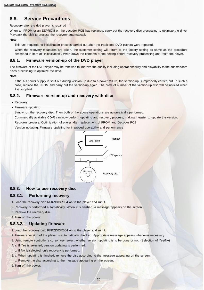
8.8.2. Firmware version-up and recovery with disc • • • • Recovery • • • • Firmware updating
Simply run the recovery disc. Then both of the above operations are automatically performed.Commercially available CD-R can now perform updating and recovery process, making it easier to update the version.Recovery process: Optimization of player after replacement of FROM and Decoder PCB.Version updating: Firmware updating for improved operability and performance
8.8.3. How to use recovery disc8.8.3.1. Performing recovery 1. Load the recovery disc RFKZD03R004 on to the player and run it. 2. Recovery is performed automatically. When it is finished, a message appears on the screen. 3. Remove the recovery disc. 4. Turn off the power.
8.8.3.2. Updating firmware 1. Load the recovery disc RFKZD03R004 on to the player and run it. 2. Firmware version of the player is automatically checked. Appropriate message appears whenever necessary. 3. Using remote controller´s cursor key, select whether version updating is to be done or not. (Selection of Yes/No) 4. a. If Yes is selected, version updating is performed.
b. If No is selected, only recovery is performed. 5. a. When updating is finished, remove the disc according to the message appearing on the screen.
b. Remove the disc according to the message appearing on the screen. 6. Turn off the power.
20
DVD-S35E / DVD-S35EB / DVD-S35EG / DVD-S31EG

9 ASSEMBLING ANDDISASSEMBLING THEMECHANISM UNIT
9.1. Disassembly Procedure
9.2. Terminal PCB 1. Unscrew the screws. 2. Remove the solders. 3. Remove the connectors.
9.3. Clamp Plate Unit 1. Push the stopper with hand to slide the tabs and remove
the clamp plate unit.
21
DVD-S35E / DVD-S35EB / DVD-S35EG / DVD-S31EG
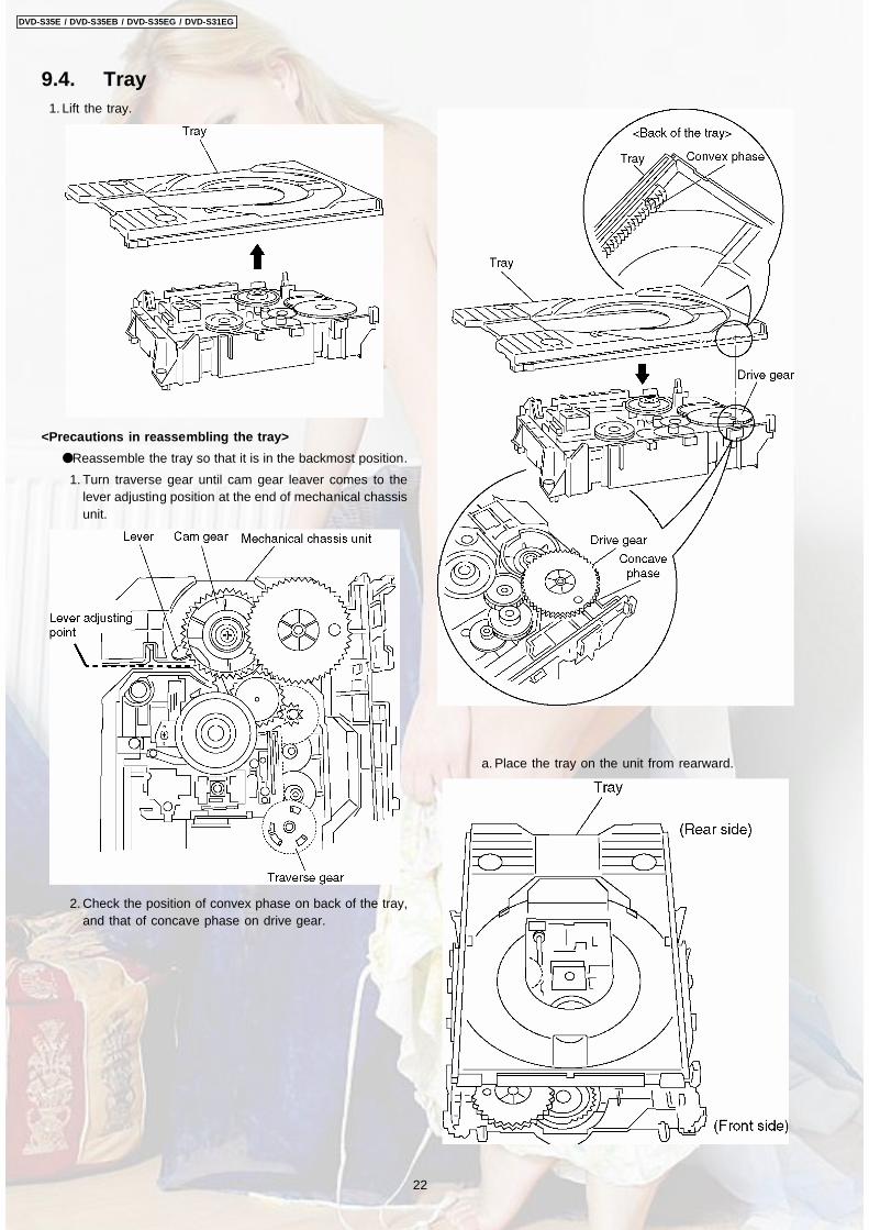
9.4. Tray 1. Lift the tray.
<Precautions in reassembling the tray> Reassemble the tray so that it is in the backmost position. 1. Turn traverse gear until cam gear leaver comes to the
lever adjusting position at the end of mechanical chassisunit.
2. Check the position of convex phase on back of the tray,and that of concave phase on drive gear.
a. Place the tray on the unit from rearward.
22
DVD-S35E / DVD-S35EB / DVD-S35EG / DVD-S31EG

b. Inch the tray frontward until convex phase andconcave phase mate.
Caution:Make sure to mate convex phase and concave phaseproperly, so that the gap between turntable and traybecomes 5mm or less.
9.5. FG PCB Unit 1. Unscrew the screw. 2. Remove the FG PCB Unit.
9.6. Traverse Block 1. Lift the traverse block while spreading the hook of the
mechanical chassis unit. 2. Disengage the tabs from the holes of the mechanical
chassis unit.
23
DVD-S35E / DVD-S35EB / DVD-S35EG / DVD-S31EG
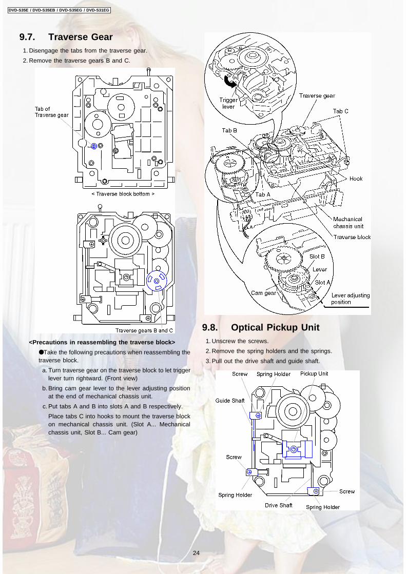
9.7. Traverse Gear 1. Disengage the tabs from the traverse gear. 2. Remove the traverse gears B and C.
<Precautions in reassembling the traverse block> Take the following precautions when reassembling thetraverse block. a. Turn traverse gear on the traverse block to let trigger
lever turn rightward. (Front view) b. Bring cam gear lever to the lever adjusting position
at the end of mechanical chassis unit. c. Put tabs A and B into slots A and B respectively.
Place tabs C into hooks to mount the traverse blockon mechanical chassis unit. (Slot A... Mechanicalchassis unit, Slot B... Cam gear)
9.8. Optical Pickup Unit 1. Unscrew the screws. 2. Remove the spring holders and the springs. 3. Pull out the drive shaft and guide shaft.
24
DVD-S35E / DVD-S35EB / DVD-S35EG / DVD-S31EG

9.8.1. Precautions in optical pickup replacementThe optical pickup can be damaged by static electricity from your body. Be sure to take static electricity countermeasureswhen working around the optical pickup. (Refer to the related page in this Manual about the countermeasures.) 1. Do not touch laser diode, actuator and their peripheries. 2. Do not use tester to check laser diode. (Laser diode can be damaged easily.) 3. The use of soldering iron with anti-static feature is recommended when providing short-circuit to laser diode or when removing
it. 4. Solder the land on flexible cable of optical pickup unit.
Caution • • • • When using the soldering iron without anti-static feature, short-circuit the flexible cable terminal with a clip before short-
circuiting the land. • • • • After intended repair is finished, remove the solder for short-circuit of laser diode in a correct way following the
procedures described in this Manual.
25
DVD-S35E / DVD-S35EB / DVD-S35EG / DVD-S31EG
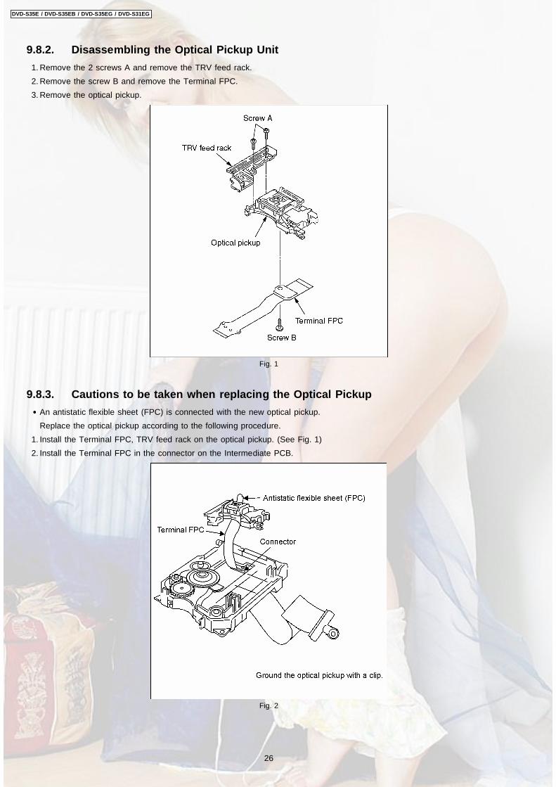
9.8.2. Disassembling the Optical Pickup Unit 1. Remove the 2 screws A and remove the TRV feed rack. 2. Remove the screw B and remove the Terminal FPC. 3. Remove the optical pickup.
Fig. 1
9.8.3. Cautions to be taken when replacing the Optical Pickup • • • • An antistatic flexible sheet (FPC) is connected with the new optical pickup.
Replace the optical pickup according to the following procedure. 1. Install the Terminal FPC, TRV feed rack on the optical pickup. (See Fig. 1) 2. Install the Terminal FPC in the connector on the Intermediate PCB.
Fig. 2
26
DVD-S35E / DVD-S35EB / DVD-S35EG / DVD-S31EG

3. Install the optical pickup unit, spring, drive shaft, guide shaft, rubber cushion, and spring holder on the traverse block.
Fig. 3
Cautions to be taken when assembling the unit: Install the pickup unit so that it is located at the rear end of the guide shaft.
27
DVD-S35E / DVD-S35EB / DVD-S35EG / DVD-S31EG

4. Cut the antistatic flexible sheet for the optical pickup unit.
Fig. 4
28
DVD-S35E / DVD-S35EB / DVD-S35EG / DVD-S31EG

9.9. Disassembling the MiddleChassis
1. Remove the holder pins. 2. Remove the tab. 3. It lifts while pulling it in the direction of the arrow.
9.10. Disassembling the TraverseGear A
1. Unscrew the screw. 2. Remove the traverse gear A.
9.11. Disassembling the SpindleMotor Unit
1. Remove the floating rubbers.
29
DVD-S35E / DVD-S35EB / DVD-S35EG / DVD-S31EG

10 ADJUSTMENT PROCEDURES10.1. Service Tools and Equipment
Application Name NumberTilt adjustment DVD test disc DVDT-S15 or DVDT-S01
Hex wrench Available on sales route.Others Screw lock RZZ0L01
Grease (1) RFKXGAK152Grease (2) RFKXPG641Oil (1) RFKXGA1280
Confirmation CD test disc PVCD-K06 or any other commerciallyavailable disc
VCD test disc PVCD-K06 or any other commerciallyavailable disc
10.2. Important points in adjustment10.2.1. Important points in optical adjustment • • • • Before starting optical adjustment, be sure to take anti-static measures. • • • • Optical pickup tilt adjustment is needed after replacement of the following components. 1. Optical pickup unit 2. Spindle motor unit 3. Optical pickup peripheral parts (such as rail)Notes
Adjustment is generally unnecessary after replacing other parts of the traverse unit. However, make adjustment if there is anoticeable degradation in picture quality. Optical adjustments cannot be made inside the optical pickup. Adjustment is generallyunnecessary after replacing the traverse unit.
10.2.2. Important points in electrical adjustment • • • • Follow the adjustment procedures described in this Manual.
10.3. Storing and Handling Test Discs • • • • Surface precision is vital for DVD test discs. Be sure to store and handle them carefully. 1. Do not place discs directly onto the workbench, etc., after use. 2. Handle discs carefully in order to maintain their flatness. Place them into their case after use and store them vertically. Store
discs in a cool place where they are not exposed to direct sunlight or air from air conditioners. 3. Accurate adjustment will not be possible if the disc is warped when placed on a surface made of glass, etc. If this happens, use
a new test disc to make optical adjustments. 4. If adjustment is done using a warped disc, the adjustment will be incorrect and some discs will not be playable.
30
DVD-S35E / DVD-S35EB / DVD-S35EG / DVD-S31EG

10.4.1.1. Adjustment procedure 1. While pressing PAUSE and OPEN/CLOSE buttons on the
main unit, press "5" on the remote control unit. 2. Confirm that "J_xxx_yyy_zz" is shown on the front display.
For your information:"yyy" and "zz" shown to the right have nothing to do withthe jitter value. "yyy" is the error counter, while "zz" isthe focus drive value.
Note:Jitter value appears on the front display.
3. Play test disc T01 (inner periphery). 4. Adjust tangential adjustment screw so that the jitter value is
minimized. 5. Play test disc T43 (outer periphery). 6. Adjust tilt adjustment screw 1 so that the jitter value is
minimized. 7. Play test disc T43 (outer periphery). 8. Adjust tilt adjustment screw 2 so that the jitter value is
minimized. 9. Repeat adjusting tilt adjustment screws 1 and 2 alternately
until the jitter value is minimized.
10.4.1.2. Important points 1. Make tangential adjustment first, and then make tilt
adjustment. 2. Repeat adjusting two or three times to find the optimum
point. 3. Finish the procedure with tilt adjustment.
Jitter value depends on the model: 1. If the jitter value changes like B, the optimum point is easy to
find.
2. If the jitter value changes like A, set the optimum point near themiddle.
10.4.1.3. Check after adjustmentPlay test disc or any other disc to make sure there is no picturedegradation in the inner, middle and outer peripheries, and noaudio skipping. After adjustment is finished, lock eachadjustment screw in position using screw lock.
10.4.1.4. Procedure for screw lock 1. After adjustment, remove top cover, tray, clamper base and
traverse unit in this sequence. 2. Lay the traverse unit upside down, and fix adjustment screw
with screw lock. 3. After fixing, reassemble traverse unit, clamper base, tray
and top cover.
10.4. Optical adjustment10.4.1. Optical pickup tilt adjustment
Measurement point Adjustment point Mode DiscTangential adjustment screwTilt adjustment screw
T01 (inner periphery) playT43 (outer periphery) play
DVDR-S15 or DVDT-S01
Measuring equipment Adjustment valueNone (Main unit display for servicing is used.) Adjust to the minimum jitter value.
31
DVD-S35E / DVD-S35EB / DVD-S35EG / DVD-S31EG

INITIAL/LOGO ABBREVIATIONSA A0~UP
ACLKAD0~UPADATAALEAMUTEAREQARFASIASOASYNC
ADDRESSAUDIO CLOCKADDRESS BUSAUDIO PES PACKET DATAADDRESS LATCH ENABLEAUDIO MUTEAUDIO PES PACKET REQUESTAUDIO RFSERVO AMP INVERTED INPUTSERVO AMPOUTPUTAUDIO WORD DISTINCTION SYNC
B BCKBCKINBDOBLKCKBOTTOMBYPBYTCK
BIT CLOCK (PCM)BIT CLOCK INPUTBLACK DROP OUTSUB CODE BLOCK CLOCKCAP. FOR BOTTOM HOLDBYPATHBYTE CLOCK
C CAVCBDOCDCDSCKCDSRDATACDRFCDVCHNDATACKSLCLVCOFTRCPACPCSCPDTCPUADRCPUADTCPUIRQCPRDCPWRCSCSYNCINCSYNCOUT
CONSTANT ANGULAR VELOCITYCAP. BLACK DROP OUTCOMPACT DISCCD SERIAL DATA CLOCKCD SERIAL DATACD RF (EFM) SIGNALCOMPACT DISC-VIDEOCHANNEL DATASYSTEM CLOCKSELECTCONSTANT LINEAR VELOCITYCAP. OFF TRACKCPU ADDRESSCPU CHIP SELECTCPU DATACPU ADDRESS LATCHCPU ADDRESS DATA BUSCPU INTERRUPT REQUESTCPU READ ENABLECPU WRITE ENABLECHIPSELECTCOMPOSITE SYNC INCOMPOSITE SYNC OUT
D DACCKDEEMPDEMPHDIG0~UPDINDMSRCKDMUTEDODOUT0~UPDRFDRPOUTDREQDRESPDSCDSLFDVD
D/A CONVERTER CLOCKDEEMPHASIS BIT ON/OFFDEEMPHASIS SWITCHINGFL DIGIT OUTPUTDATA INPUTDM SERIAL DATA READ CLOCKDIGITAL MUTE CONTROLDROP OUTDATAOUTPUTDATA SLICE RF (BIAS)DROP OUT SIGNALDATA REQUESTDATA RESPONSEDIGITAL SERVO CONTROLLERDATA SLICE LOOP FILTERDIGITAL VIDEO DISC
INITIAL/LOGO ABBREVIATIONSE EC
ECR
ENCSELETMCLKETSCLK
ERROR TORQUE CONTROLERROR TORQUE CONTROLREFERENCEENCODER SELECTEXTERNAL M CLOCK (81MHz/40.5MHz)EXTERNAL S CLOCK (54MHz)
F FBALFCLKFEFFIFEOFGFSCFSCK
FOCUS BALANCEFRAME CLOCKFOCUS ERRORFOCUS ERROR AMP INVERTED INPUTFOCUS ERROR AMP OUTPUTFREQUENCY GENERATORFREQUENCY SUB CARRIERFS (384 OVER SAMPLING) CLOCK
G GND COMMON GROUNDING (EARTH)H HA0~UP
HD0~UPHINTHRXW
HOST ADDRESSHOST DATAHOST INTERRUPTHOST READ/WRITE
I IECOUTIPFRAGIREFISEL
IEC958 FORMAT DATA OUTPUTINTERPOLATION FLAGI (CURRENT) REFERENCEINTERFACE MODE SELECT
L LDONLPCLRCK
LASER DIODE CONTROLLASER POWER CONTROLL CH/R CH DISTINCTION CLOCK
M MA0~UPMCKMCKIMCLKMDATAMDQ0~UPMDQMMLDMPEG
MEMORY ADDRESSMEMORY CLOCKMEMORY CLOCK INPUTMEMORY SERIAL COMMAND CLOCKMEMORY SERIAL COMMAND DATAMEMORY DATA INPUT/OUTPUTMEMORY DATA I/O MASKMEMORYSERIAL COMMAND LOADMOVING PICTURE EXPERTS GROUP
O ODCOFTROSCIOSCOOSD
OPTICAL DISC CONTROLLEROFF TRACKINGOSCILLATOR INPUTOSCILLATOR OUTPUTON SCREEN DISPLAY
P P1~UPPCDPCKPDVDPEAKPLLCLKPLLOKPWMCTLPWMDAPWMOA, B
PORTCD TRACKING PHASE DIFFERENCEPLL CLOCKDVD TRACKING PHASE DIFFERENCECAP. FOR PEAK HOLDCHANNEL PLL CLOCKPLL LOCKPWM OUTPUT CONTROLPULSE WAVE MOTOR DRIVEAPULSE WAVE MOTOR OUT A, B
11 Abbreviations
32
DVD-S35E / DVD-S35EB / DVD-S35EG / DVD-S31EG
INITIAL/LOGO ABBREVIATIONSR RE
RFENVRFORSRSELRSTRSV
READ ENABLERF ENVELOPERF PHASE DIFFERENCE OUTPUT(CD-ROM) REGISTER SELECTRF POLARITY SELECTRESETRESERVE
S SBI0, 1SBO0SBT0, 1SCKSCKRSCLSCLKSDASEG0~UPSELCLKSENSIN1, 2SOUT1, 2SPDISPDOSPENSPRCLKSPWCLKSQCKSQCXSRDATASRMADRSRMDT0~7SSSTATSTCLKSTD0~UPSTENABLESTSELSTVALIDSUBCSBCKSUBQSYSCLK
SERIAL DATA INPUTSERIAL DATA OUTPUTSERIAL CLOCKSERIAL DATA CLOCKAUDIO SERIAL CLOCK RECEIVERSERIAL CLOCKSERIAL CLOCKSERIAL DATAFL SEGMENT OUTPUTSELECTCLOCKSERIAL PORT ENABLESERIAL DATA INSERIAL DATA OUTSERIAL PORT DATA INPUTSERIAL PORT DATA OUTPUTSERIAL PORT R/W ENABLESERIAL PORT READ CLOCKSERIAL PORT WRITE CLOCKSUB CODE Q CLOCKSUBCODE Q DATA READ CLOCKSERIAL DATASRAM ADDRESS BUSSRAM DATA BUS 0~7START/STOPSTATUSSTREAM DATA CLOCKSTREAM DATASTREAM DATA INPUT ENABLESTREAM DATA POLARITY SELECTSTREAM DATAVALIDITYSUB CODE SERIALSUB CODE CLOCKSUB CODE Q DATASYSTEM CLOCK
T TETIBALTIDTINTIPTISTPSNTPSOTPSPTRCRSTRONTRSON
TRACKING ERRORBALANCE CONTROLBALANCE OUTPUT 1BALANCE INPUTBALANCE INPUTBALANCE OUTPUT 2OP AMP INPUTOP AMP OUTPUTOP AMP INVERTED INPUTTRACK CROSSSIGNALTRACKING ONTRAVERSE SERVO ON
INITIAL/LOGO ABBREVIATIONSV VBLANK
VCC
VCDCONT
VDDVFBVREFVSS
V BLANKINGCOLLECTOR POWER SUPPLYVOLTAGEVIDEO CD CONTROL (TRACKINGBALANCE)DRAIN POWER SUPPLY VOLTAGEVIDEO FEED BACKVOLTAGE REFERENCESOURCE POWER SUPPLYVOLTAGE
W WAITWDCKWEHWSR
BUS CYCLE WAITWORD CLOCKWRITE ENABLE HIGHWORD SELECT RECEIVER
X XXALEXAREQXCDROMXCSXCSYNCXDSXHSYNCOXHINTXIXINTXMWXOXREXSRMCEXSRMOEXSRMWEXVCSXVDSXVSYNCO
X´ TALX ADDRESS LATCH ENABLEX AUDIO DATA REQUESTX CD ROM CHIP SELECTX CHIP SELECTX COMPOSITE SYNCX DATA STROBEX HORIZONTAL SYNC OUTPUTXH INTERRUPTREQUESTX´ TAL OSCILLATOR INPUTX INTERRUPTX MEMORY WRITE ENABLEX´ TAL OSCILLATOR OUTPUTX READ ENABLEX SRAM CHIP ENABLEX SRAM OUTPUT ENABLEX SRAM WRITE ENABLEX V-DEC CHIPSELECTX V-DEC CONTROL BUS STROBEX VERTICAL SYNC OUTPUT
33
DVD-S35E / DVD-S35EB / DVD-S35EG / DVD-S31EG
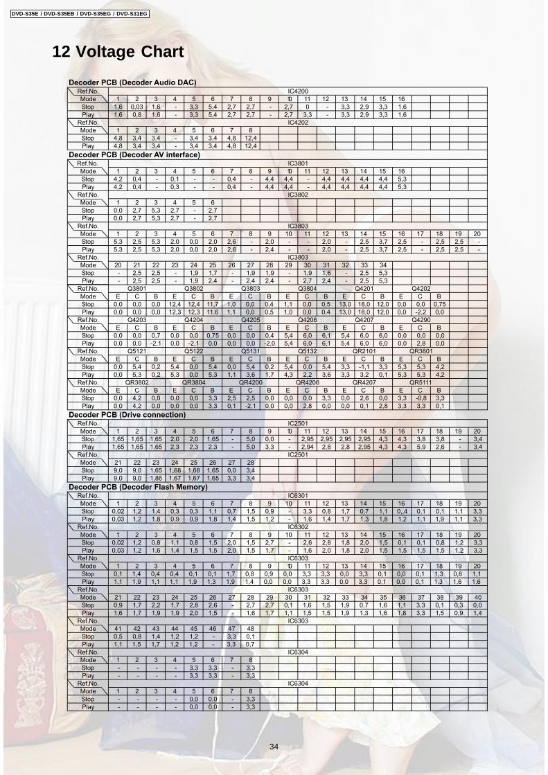
12 Voltage ChartDecoder PCB (Decoder Audio DAC)
Ref.No.
Mode 1 2 3 4 5 6 7 8 9 10 11 12 13 14 15 16
Stop 1,6 0,03 1,6 - 3,3 5,4 2,7 2,7 - 2,7 0 - 3,3 2,9 3,3 1,6
Play 1,6 0,8 1,6 - 3,3 5,4 2,7 2,7 - 2,7 3,3 - 3,3 2,9 3,3 1,6
Ref.No.
Mode 1 2 3 4 5 6 7 8
Stop 4,8 3,4 3,4 - 3,4 3,4 4,8 12,4
Play 4,8 3,4 3,4 - 3,4 3,4 4,8 12,4
Decoder PCB (Decoder AV interface)Ref.No.
Mode 1 2 3 4 5 6 7 8 9 10 11 12 13 14 15 16
Stop 4,2 0,4 - 0,1 - - 0,4 - 4,4 4,4 - 4,4 4,4 4,4 4,4 5,3
Play 4,2 0,4 - 0,3 - - 0,4 - 4,4 4,4 - 4,4 4,4 4,4 4,4 5,3
Ref.No.
Mode 1 2 3 4 5 6
Stop 0,0 2,7 5,3 2,7 - 2,7
Play 0,0 2,7 5,3 2,7 - 2,7
Ref.No.
Mode 1 2 3 4 5 6 7 8 9 10 11 12 13 14 15 16 17 18 19 20
Stop 5,3 2,5 5,3 2,0 0,0 2,0 2,6 - 2,0 - - 2,0 - 2,5 3,7 2,5 - 2,5 2,5 -
Play 5,3 2,5 5,3 2,0 0,0 2,0 2,6 - 2,4 - - 2,0 - 2,5 3,7 2,5 - 2,5 2,5 -
Ref.No.
Mode 20 21 22 23 24 25 26 27 28 29 30 31 32 33 34
Stop - 2,5 2,5 - 1,9 1,7 - 1,9 1,9 - 1,9 1,6 - 2,5 5,3
Play - 2,5 2,5 - 1,9 2,4 - 2,4 2,4 - 2,7 2,4 - 2,5 5,3
Ref.No.
Mode E C B E C B E C B E C B E C B E C B
Stop 0,0 0,0 0,0 12,4 12,4 11,7 1,0 0,0 0,4 1,1 0,0 0,5 13,0 18,0 12,0 0,0 0,0 0,75
Play 0,0 0,0 0,0 12,3 12,3 11,6 1,1 0,0 0,5 1,0 0,0 0,4 13,0 18,0 12,0 0,0 -2,2 0,0
Ref.No.
Mode E C B E C B E C B E C B E C B E C B
Stop 0,0 0,0 0,7 0,0 0,0 0,75 0,0 0,0 0,4 5,4 6,0 6,1 5,4 6,0 6,0 0,0 0,0 0,0
Play 0,0 0,0 -2,1 0,0 -2,1 0,0 0,0 0,0 -2,0 5,4 6,0 6,1 5,4 6,0 6,0 0,0 2,8 0,0
Ref.No.
Mode E C B E C B E C B E C B E C B E C B
Stop 0,0 5,4 0,2 5,4 0,0 5,4 0,0 5,4 0,2 5,4 0,0 5,4 3,3 -1,1 3,3 5,3 5,3 4,2
Play 0,0 5,3 0,2 5,3 0,0 5,3 1,1 3,6 1,7 4,3 2,2 3,6 3,3 3,2 0,1 5,3 5,3 4,2
Ref.No.
Mode E C B E C B E C B E C B E C B E C B
Stop 0,0 4,2 0,0 0,0 0,0 3,3 2,5 2,5 0,0 0,0 0,0 3,3 0,0 2,6 0,0 3,3 -0,8 3,3
Play 0,0 4,2 0,0 0,0 0,0 3,3 0,1 -2,1 0,0 0,0 2,8 0,0 0,0 0,1 2,8 3,3 3,3 0,1
Decoder PCB (Drive connection)Ref.No.
Mode 1 2 3 4 5 6 7 8 9 10 11 12 13 14 15 16 17 18 19 20
Stop 1,65 1,65 1,65 2,0 2,0 1,65 - 5,0 0,0 - 2,95 2,95 2,95 2,95 4,3 4,3 3,8 3,8 - 3,4
Play 1,65 1,65 1,65 2,3 2,3 2,3 - 5,0 3,3 - 2,94 2,8 2,8 2,95 4,3 4,3 5,9 2,6 - 3,4
Ref.No.
Mode 21 22 23 24 25 26 27 28
Stop 9,0 9,0 1,65 1,68 1,68 1,65 0,0 3,4
Play 9,0 9,0 1,86 1,67 1,67 1,65 3,3 3,4
Decoder PCB (Decoder Flash Memory)Ref.No.
Mode 1 2 3 4 5 6 7 8 9 10 11 12 13 14 15 16 17 18 19 20
Stop 0,02 1,2 1,4 0,3 0,3 1,1 0,7 1,5 0,9 - 3,3 0,8 1,7 0,7 1,1 0,,4 0,1 0,1 1,1 3,3
Play 0,03 1,2 1,8 0,9 0,9 1,8 1,4 1,5 1,2 - 1,6 1,4 1,7 1,3 1,8 1,2 1,1 1,9 1,1 3,3
Ref.No.
Mode 1 2 3 4 5 6 7 8 9 10 11 12 13 14 15 16 17 18 19 20
Stop 0,02 1,2 0,8 1,1 0,8 1,5 2,0 1,5 2,7 - 2,6 2,8 1,8 2,0 1,5 0,1 0,1 0,8 1,2 3,3
Play 0,03 1,2 1,6 1,4 1,5 1,5 2,0 1,5 1,7 - 1,6 2,0 1,8 2,0 1,5 1,5 1,5 1,5 1,2 3,3
Ref.No.
Mode 1 2 3 4 5 6 7 8 9 10 11 12 13 14 15 16 17 18 19 20
Stop 0,1 1,4 0,4 0,4 0,1 0,1 1,7 0,8 0,9 0,0 3,3 3,3 0,0 3,3 0,1 0,0 0,1 1,3 0,8 1,1
Play 1,1 1,9 1,1 1,1 1,9 1,3 1,9 1,4 0,0 0,0 3,3 3,3 0,0 3,3 0,1 0,0 0,1 1,3 1,6 1,6
Ref.No.
Mode 21 22 23 24 25 26 27 28 29 30 31 32 33 34 35 36 37 38 39 40
Stop 0,9 1,7 2,2 1,7 2,8 2,6 - 2,7 2,7 0,1 1,6 1,5 1,9 0,7 1,6 1,1 3,3 0,1 0,3 0,0
Play 1,6 1,7 1,9 1,9 2,0 1,5 - 1,6 1,7 1,1 1,5 1,5 1,9 1,3 1,6 1,8 3,3 1,5 0,9 1,4
Ref.No.
Mode 41 42 43 44 45 46 47 48
Stop 0,5 0,8 1,4 1,2 1,2 - 3,3 0,1
Play 1,1 1,5 1,7 1,2 1,2 - 3,3 0,7
Ref.No.
Mode 1 2 3 4 5 6 7 8
Stop - - - - 3,3 3,3 - 3,3
Play - - - - 3,3 3,3 - 3,3
Ref.No.
Mode 1 2 3 4 5 6 7 8
Stop - - - - 0,0 0,0 - 3,3
Play 0,0 0,0 3,3
IC4200
IC4202
IC3801
IC3802
Q4205 Q4206
IC3803
IC3803
Q3801 Q3802 Q3803 Q3804 Q4201 Q4202
Q4207 Q4290
Q5121 Q5122 Q5131 Q5132 QR2101 QR3801
Q4203 Q4204
QR4207 QR5111
IC2501
IC2501
QR3802 QR3804 QR4200 QR4206
IC6303
IC6304
IC6304
IC6301
IC6302
IC6303
IC6303
- - - - -
DVD-S35E / DVD-S35EB / DVD-S35EG / DVD-S31EG
34

Decoder PCB (AV-Decoder)Ref.No.
Mode 1 2 3 4 5 6 7 8 9 10 11 12 13 14 15 16
Stop 3,3 - 1,6 1,6 3,3 - 1,6 1,6 - 1,6 - 3,3 1,6 3,3 1,6 3,3
Play 3,3 - 1,6 1,6 3,3 - 1,6 1,6 - 1,6 - 3,3 1,6 3,3 1,6 3,3
Ref.No.
Mode 1 2 3 4 5 6 7 8 9 10 11 12 13 14 15 16 17 18 19 20
Stop 3,3 - 3,3 - 3,3 1,5 - 0,0 3,3 2,7 0,8
Play 3,3 - 3,3 - 3,3 1,5 - 0,0 3,3 1,7 1,5
Ref.No.
Mode 21 22 23 24 25 26 27 28 29 30 31 32 33 34 35 36 37 38 39 40
Stop 0,7 0,1 1,3 - 0,1 0,0 1,4 0,1 0,0 - 0,1 1,8 2,3 1,6 1,1 0,1 1,5 0,1 0,1 0,1
Play 1,1 1,1 1,3 - 0,1 0,0 1,7 1,4 0,0 - 1,5 1,8 1,6 1,6 1,4 1,4 1,5 1,3 0,1 0,0
Ref.No.
Mode 41 42 43 44 45 46 47 48 49 50 51 52 53 54 55 56 57 58 59 60
Stop 0,1 3,3 - 1,4 1,5 2,7 0,0 0,0 3,3 0,0 3,3 0,0 3,3 3,3 3,3 3,3 - - 2,9 3,3
Play 1,8 3,3 - 1,4 1,6 1,7 0,0 0,0 0,0 0,0 3,3 0,0 3,3 3,3 3,3 3,3 - - 2,9 3,3
Ref.No.
Mode 61 62 63 64 65 66 67 68 69 70 71 72 73 74 75 76 77 78 79 80
Stop 1,1 2,9 2,7 0,9 3,3 3,3 1,5 3,3 - 1,6 1,6 0,0 3,3 0,0 3,3 3,3 0,0 3,3 3,3 -
Play 1,1 2,9 2,7 0,9 3,3 0,9 1,5 3,3 - 1,6 2,3 0,0 0,0 3,3 0,0 3,3 0,0 3,3 3,3 -
Ref.No.
Mode 81 82 83 84 85 86 87 88 89 90 91 92 93 94 95 96 97 98 99 100
Stop 3,3 0,0 3,3 - 0,0 0,0 0,0 0,0 0,0 0,0 3,3 1,6 - - - - - 1,5 - -
Play 3,3 0,0 3,3 - 0,0 0,0 0,0 0,0 0,0 0,0 3,3 1,6 - - - - - 1,5 - -
Ref.No.
Mode 101 102 103 104 105 106 107 108 109 110 111 112 113 114 115 116 117 118 119 120
Stop - - - 3,3 0,8 - 0,7 1,5 2,0 2,5 1,9 1,1 2,0 2,0 1,8 1,4 1,0 3,3 - 1,8
Play - - - 3,3 0,8 - 0,7 1,5 2,0 2,5 1,9 1,1 2,0 1,7 1,8 1,4 1,0 3,3 - 1,8
Ref.No.
Mode 121 122 123 124 125 126 127 128 129 130 131 132 133 134 135 136 137 138 139 140
Stop 1,8 2,2 2,2 2,2 2,2 2,2 2,2 2,2 2,2 2,2 2,2 0,0 0,2 0,0 0,0 2,2 1,6 - 1,2 1,6
Play 1,8 2,2 2,2 2,2 2,2 2,2 2,2 2,2 2,2 2,2 2,2 0,5 1,7 0,0 0,0 2,2 1,6 - 1,6 1,6
Ref.No.
Mode 141 142 143 144 145 146 147 148 149 150 151 152 153 154 155 156 157 158 159 160
Stop 1,6 1,6 0,7 1,5 3,3 2,6 1,6 1,6 3,3 1,6 - 1,6 3,3 1,3 - 2,1 3,3 0,1 - 0,4
Play 1,6 1,6 0,8 1,5 3,3 2,3 1,6 2,2 3,3 1,6 - 1,6 3,3 1,3 - 2,1 3,3 0,1 - 0,4
Ref.No.
Mode 161 162 163 164 165 166 167 168 169 170 171 172 173 174 175 176 177 178 179 180
Stop 0,4 0,0 2,3 0,8 1,6 3,3 - 0,0 - 1,6 3,3 1,6 - 1,6 1,6 0,0 - - - 0,0
Play 0,4 0,0 2,3 0,8 1,6 3,3 - 0,0 - 1,6 3,3 1,6 - 1,6 1,6 0,8 - - - 0,8
Ref.No.
Mode 181 182 183 184 185 186 187 188 189 190 191 192 193 194 195 196 197 198 199 200
Stop 1,6 3,3 - 2,5 2,2 1,5 2,5 2,5 3,3 2,5 2,5 2,5 - 3,3 -
Play 1,6 3,3 - 2,5 3,0 1,5 2,5 2,5 3,3 2,5 2,2 3,2 - 3,3 -
Ref.No.
Mode 201 202 203 204 205 206 207 208 209 210 211 212 213 214 215 216 217 218 219 220
Stop 3,3 - 2,5 3,3 - 0,0 1,6 0,3 - 0,0 1,6 0,1 3,3 1,5
Play 3,3 - 2,5 3,3 - 0,0 1,6 0,6 - 0,0 1,7 0,3 3,3 1,5
Ref.No.
Mode 221 222 223 224 225 226 227 228 229 230 231 232 233 234 235 236 237 238 239 240
Stop - 0,0 1,8 - 1,8 3,3 0,0 0,0 0,0 - 0,1 3,1 3,3 1,5 3,3 - 1,6 2,9 3,1 3,3
Play - 0,0 1,8 - 1,8 3,3 0,1 0,0 0,0 - 0,1 3,1 3,3 1,5 3,3 - 1,6 2,7 3,1 3,3
Ref.No.
Mode 241 242 243 244 245 246 247 248 249 250 251 252 253 254 255 256
Stop - 3,0 1,5 - 2,1 - 3,3 -
Play - 3,0 1,5 - 1,7 - 3,3 -
Ref.No.
Mode 1 2 3 4 5 6 7 8 9 10 11 12 13 14 15 16 17 18 19 20
Stop 3,3 3,3 - 3,3 - - 3,3 3,1 3,1 0,0 2,7
Play 3,3 3,3 - 3,3 - - 3,3 3,1 3,1 0,7 27,7
Ref.No.
Mode 21 22 23 24 25 26 27 28 29 30 31 32 33 34 35 36 37 38 39 40
Stop 0,0 1,5 1,5 0,0 0,0 0,1 0,1 3,3 1,4 - 3,3 -
Play 0,0 1,5 1,5 0,0 0,1 0,2 0,0 3,3 1,4 - 3,3 -
Ref.No.
Mode 41 42 43 44 45 46 47 48 49 50 51 52 53 54 55 56 57 58 59 60
Stop 3,3 3,3 - - 3,3 - 3,3 - - 1,6
Play 3,3 3,3 - - 3,3 - 3,3 - - 1,6
Ref.No.
Mode 61 62 63 64 65 66 67 68 69 70 71 72 73 74 75 76 77 78 79 80
Stop 1,6 1,6 1,5 0,0 0,0 0,0 3,3 1,8 1,5 1,3 - - 3,3 -
Play 1,6 1,6 1,,5 0,0 0,0 0,0 3,3 1,8 0,0 1,3 - - 3,3 -
Ref.No.
Mode 81 82 83 84 85 86
Stop 3,3 - -
Play 3,3 - -
Ref.No.
Mode 1 2 3 4 5
Stop - - - 3,3 3,3
Play - - - 3,3 3,3
IC2002
IC2002
IC2003
IC3001
IC2002
IC2002
IC2002
IC3001
IC3001
IC3001
IC3001
IC3001
IC3001
IC3001
IC3001
IC3001
IC3001
IC3001
IC3001
IC6561
DVD-S35E / DVD-S35EB / DVD-S35EG / DVD-S31EG
35

Front Panel PCB UnitRef.No.
Mode 1 2 3 4 5 6 7 8 9 10 11 12 13 14 15 16 17 18 19 20
Stop -22 -22 -22 -22 -22 -22 -22 -22 3,5 -21,9 -22 -23,5 -0,1 -23,5 -20,8 -23,5 -0,1 -0,1 -0,1 -0,1
Play -22 -22 -22 -22 -22 -22 -22 -22 3,5 -22 -22 0,0 0,0 -23,5 -23,5 -23,5 12 -24,2 0,05 -0,1
Ref.No.
Mode 21 22 23 24 25 26 27 28 29 30 31 32 33 34 35 36 37 38 39 40
Stop -0,1 -0,1 -0,1 -21 -21 -21 3,5 -0,6 -23,8 -1,3 3,5 0,0 3,5 3,3 3,5 3,5 2,7 2,9 3,5 3,5
Play -21 -0,06 - -0,1 -21 -21 3,5 0,0 -0,1 0,0 3,5 0,0 3,5 3,3 3,5 0,0 2,7 2,9 3,5 3,5
Ref.No.
Mode 41 42 43 44 45 46 47 48 49 50 51 52 53 54 55 56 57 58 59 60
Stop 1,7 1,7 3,5 - 3,5 3,5 3,5 3,5 -0,02 0,7 0,3 0,0 0,0 3,5 3,5 3,3 - 1,7 1,9 3,5
Play 1,7 1,7 3,5 - 3,5 3,5 3,5 3,5 -0,03 0,7 0,3 0,0 0,0 3,5 3,5 3,3 - 1,7 1,9 3,5
Ref.No.
Mode 61 62 63 64
Stop - 3,5 0,4 3,3
Play - 3,5 3,5 3,3
Ref.No.
Mode E C B E C B E C B
Stop -20,4 -20,0 -19,7 -3,5 13,4 -3,5 0,0 0,0 3,4
Play -20,6 -20,6 -20,0 -3,5 13,5 -3,5 0,0 0,0 3,4
Q6091 QR6081 QR6101
IC6001
IC6001
IC6001
IC6001
Power PCBRef.No.
Mode 1 2 3 4 5 6 7 8 9 10 11 12 13 14 15 16 17 18 19 20
Stop 0,0 0,0 0,0 ~145 ~145 - 0,0 -
Play 0,0 0,0 0,0 ~145 ~145 - 0,0 -
Ref.No.
Mode 1 2 3 4 5 6 7 8 9 10 11 12 13 14 15 16 17 18
Stop - 3,3 3,3 1,7 3,3 3,3 2,9 2,7 - 1,0 0,0 3,3 3,3 - - -16,9 -24 -20,5
Play - 3,3 3,3 1,7 3,3 3,3 2,9 2,7 - 0,0 0,0 3,3 3,3 - - -16,9 -24 -20,5
Ref.No.
Mode 1 2 3 4 5 6 7 8 9 10 11 12 13 14 15 16 17 18 19
Stop - 3,3 3,3 3,3 1,7 1,5 - 9,0 - 5,0 - 6,0 - 18 0,0 0,0 2,9 2,7 0,0
Play - 3,3 3,3 3,3 1,7 1,5 - 9,0 - 5,0 - 6,0 - 18 0,0 0,0 2,9 2,7 0,0
Ref.No.
Mode E C B E C B E C B E C B E C B E C B
Stop 5,1 5,3 5,9 12 9,1 12 3,5 6,0 4,0 1,9 2,7 2,5 1,5 2,5 1,9 0,0 12,0 0,0
Play 5,1 5,3 5,8 11,6 9,1 11,6 3,5 6,0 4,0 1,9 2,5 2,7 1,5 2,5 1,9 0,0 11,6 0,0
IC1001
PS1102
Q1101 Q1102 Q1170 Q1172 Q1173
PP1101
QR1101
DVD-S35E / DVD-S35EB / DVD-S35EG / DVD-S31EG
36
13 BLOCK DIAGRAM13.1. OVERALL BLOCK DIAGRAM
FRONT PCB
MOTORTRAVERSE
TRAY
IC6302IC6001
IC2501
MECHANISM UNIT DECODER PCB
IC3001 IC3801JK3801
JK3802
IC3803
IC4200
IC3804
IC4202
OPTICAL
DECODERAV
MICONFRONT
KEY
REMOTE CTL
LED
FL
IC6303
FLASH
LATCH
LATCH
MEMORY
IC6301
DRIVEMOTOR
VIDEO DRIVER
VIDEO SIGNAL
MOTORSPINDLE
UNITPICK UPOPTICAL
161 2
1R
R
R / CR
Y
DMIXOUT
S/PDIF
GG / Y
B
B / CB
C
L
L
CB CR
Y CVBS
R
3
7
19
15
11
14 6 2
4
33
22
6
7 12
25
19
2
4 10
31
160
158
163
164
176
181
IC3802
S-VHS
DRIVER
EEPROM
AUDIODRIVER
DUALAMP.
TRANSMITT.IC
IC6304
no service partmust replace PCB Unit
DVD-S35E / DVD-S35EB / DVD-S35EG / DVD-S31EG
37

13.2. POWER BLOCK DIAGRAM
+
SECONDARY CIRCUITPRIMARY CIRCUIT
Q1001
IC1001
CONTROLVOLTAGECONSTANT
NSW+5.6V
FLH-
FLH+
M+9V
NSW +3.3V
FL-24.6V
SW 1.5V
D+5V
NSW+16V
REG.SHUNT IC1102
15
16
Q1101
Q1102
Q1170
11
18
17
12
14
REG.13
10
TRANSFORMERPOWER
T1001
D1101
D1102
D1104
D1107
D1108
D1106
C1117
C1001,C1013
D1001, D1002D1003, D1004
RECTIFIER
L1001
FILTERLINE
D1007
KILLERSURGE
F1001
AC SOCKET
P1001
REG.
REG.
COUPLERPHOTO
DVD-S35E / DVD-S35EB / DVD-S35EG / DVD-S31EG
38

13.3. FRONT PANEL BLOCK DIAGRAM
S6052 S6051 S6050
S6062 S6061 S6060
04S6 1
S6101
D6101
IC6101
FRONT LEFT PCB
SMALL ZOOM RVS-SKIP FWD-SKIP
STOP PLAY PAUSE
D6081
ZOOM-LED
STBY-LED
POWER
IR RECIVER
FRONT RIGHT PCB
S6053S6054
LARGE
NOPE /CLOSE
X6001
ZOOM-LEDDRIVE
63
43
46
64
47
48
58
59
IC6001
FIP
DL6001
1
20
12
11
26
28
29
16
P1 - P2
REMOCON
WIDE (H)
CF1
CF2
AN2
AN1
AN0
POFF (L)
P3 - P9
P12 - P16
1G - 10G
DVD-S35E / DVD-S35EB / DVD-S35EG / DVD-S31EG
39
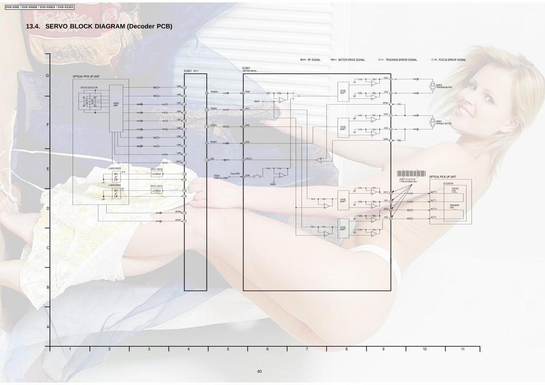
13.4. SERVO BLOCK DIAGRAM (Decoder PCB)
BIAS1
BIAS2
-+
SHIFT
-
LEVEL
+
+-
+-
SHIFT
-
LEVEL
+
-+
+-
SHIFT
-
LEVEL
+
+-
+-
SHIFTLEVEL
-+
+-
+-
OPIN-5
OPIN+4
SPINDLE MOTORM2601
TRAVERS MOTORM2602
IC6001-41,42PINFROM LDIN
24
OPOUT6
AD0
1.2Vp-p(0.5usec./div.)IC2511-11,12,13,14
RF SIGNAL MOTOR DRIVE SIGNAL TRACKING ERROR SIGNAL FOCUS ERROR SIGNAL
VIN3
VIN2
VIN1
TRIN
SPDRV
FODRV
TRDRV
TRSDRV
VO2-
VO2+
VO1-
VO1+
VO3-
VO3+
VO4-
VO4+
71
70
2
26
11
12
13
14
18
17
16
15
23
3
(MOTOR DRIVE)IC2501
ACT F-
ACT F+
ACT T-
ACT T+
OPTICAL PICK UP UNIT
ACTUATOR
COILTRACKING
COILFOCUS
RFINN
RFINP
LASER DIODE Q5121, Q5122
LD DRIVE
VIN10
VIN9
VIN4
VIN3
VIN2
VIN1
VIN8
VIN7
VIN6
VIN5
OPTICAL PICK UP UNIT
PHOTO DETECTOR
B3B4
B2B1
A3
A2
A4
A1
LASER DIODE
AMPHEAD
Q5131, Q5132
LD DRIVE
122
(DV1)IC3001
123
124
125
126
127
128
129
130
131
133
132
135
134
120
121
148
152
150
F
G
E
D
C
B
A
54321 9 10876 11
DVD
CD
Tray DRV
DVD-S35E / DVD-S35EB / DVD-S35EG / DVD-S31EG
40

14 SCHEMATIC DIAGRAM14.1. INTERCONNECTION SCHEMATIC DIAGRAM
F
G
E
D
C
B
A
54321 9 10876 11
1 TRAY-SW(-)2 D GND
5
DT
R-
S
P-M
OO
SP - O OD M T R-
FG3
T
R6
S
PD
-MO
O+
SPD- O OM T R+
FG2
7 T
RV
-T
R-
MO
O
V- O OTR M T R-
FG2
8
RV
-T
R
TM
OO
+
V- O O +TR M T R
FG1
4
N(F
G
D
G2
)
2)GND (FG
2
F
G3
FG3
R
-3
T
VS
W
V- WTR S
5
1
6
2
7
3
8
4
4
3
2
1
JK3802 IC3804P1001
COX
JK3801
Terminal PCB Unit
FG PCB Unit
Mechanism Unit
FP5101
FP2501
T(+)
F(+)
F(-)
T(-)
3.3V HFM
GND
LD(+)(DVD)
GND
GND
RF P
RF N
F1(DVD)
F2(DVD)
GAIN H/L
P IN(DVD)
V REF2.2(DVD)
TA(DVD)
TD(DVD)
TC(DVD)
TB(DVD)
VCC 5V
FE1
GND
LD(+)(CD)
T1(CD)
V REF2.2(CD)
FE2(CD)
T2(CD)
P IN(CD)
GND
30
29
28
27
26
25
24
23
22
21
20
19
18
17
16
15
14
13
12
11
9
10
8
7
6
5
4
3
2
1
SWITCHOPENTRAY
Decoder PCB Unit
Power PCB Unit
Front PCB Unit
PS
2001
PP
1101
FIP
9
DG
ND
DG
ND
7
DS
PC
LK
DS
PC
LK
8 S
TA
TS
TA
T
9 10
12
11
13
14
15
16
17
187 8
PS
1102
PP
6001
11
D
GN
DD
GN
D
6 T
RA
Y-M
UT
ET
RA
Y-M
UT
E
5 T
RA
Y/T
RV
-SW
TR
AY
/TR
V-S
W
4
TR
AY
DR
VT
RA
YD
RV
2 T
RA
Y-C
LO
SE
TR
AY
-CL
OS
E
3 T
RA
Y-O
PE
NT
RA
Y-O
PE
N
6542 3
Optical Pickup Unit
Front PCB Unit PP6101
P1103
FC6101
FP2601
FP2602
1 F
G1
FG1
10
C
MD
CM
D
11
N
P-M
UT
EN
P-M
UT
E
12
N
SW
+3
.3V
NS
W+
3.3
V
13
P
OF
F (
L)
PO
FF
(L
)
14
D
GN
DD
GN
D
15
D
GN
DD
GN
D
16
F
LH
+F
LH
+
17
F
L-2
4.6
VF
L-2
4.6
V
18
F
-LH
-F
-LH
-
1
5
4
2
3
1
5
4
2
3
STBLEDSTBLEDNSW+3.3VNSW+3.3VPOWER-SWPOWER-SWREMOCONREMOCONDGNDDGND
66
55
44
33
22
11
77
88
99
10
10
11
11
12
12
13
13
14
14
15
15
16
16
17
17
18
18
19
19
SW
+1
.5V
SW
+1
.5V
GN
DG
ND
NS
W+
16
VN
SW
+1
6V
GN
DG
ND
D+
5V
D+
5V
GN
DG
ND
M+
9V
M+
9V
GN
DG
ND
CM
DC
MD
DS
PC
LK
DS
PC
LK
STA
TU
SS
TA
TU
SN
P_M
UT
EN
P_M
UT
E
NS
W+
5.6
VN
SW
+5
.6V
TR
AY
-MU
TE
TR
AY
-MU
TE
TR
AY
TR
V-S
WT
RA
YT
RV
-SW
TR
AY
DR
VT
RA
YD
RV
TR
AY
-CLO
SE
TR
AY
-CLO
SE
M9V
-CT
LM
9V
-CT
L
GN
DG
ND
DVD-S35E / DVD-S35EB / DVD-S35EG / DVD-S31EG
41

14.2. POWER PCB UNIT
GND
R1001*(spare)
L1001ELF15N004A
D11
50
VW
J00
23
=5
D1151VWJ0023=5
D1152
VW
J00
23
=5
1 2
3
456
7
8
SoftS FB
VCC
D1D2N.C.
Isense
GND
IC1001ICE2A165
M9V-CTLM9V-CTL
GND
D1006ERA22-04V5
C110125V120 [RJB]
NP-MUTE
TRAY-CLOSE
L110210u
TRAYDRV
TRAYTRV-SW
TRAY-MUTE
NP-MUTE
NP-MUTE
TRAY-MUTE
R1102
10 [0.5W]
TRAY-MUTE
C1103
2200p
TRAYTRV-SW
TRAYTRV-SWTRAYDRV
TRAYDRVTRAY-CLOSE
TRAY-CLOSE
R110610 [1W]
L1103
10u
DSPCLKSTAT
CMD
N_SW+16V
CMD
NSW5.6V
DSPCLKSTAT
D+5V
GND
SW+1.5V
DGNDTRAY-OPEN
DGND
DGND
POFF(L)
D1107
ERA22-04V5
TRAY-CLOSE
TRAY-OPEN
FL-24.6V
NSW+3.3V
DGND
FLH-
FLH+
R1116*(spare)
CMD
DSPCLK
STAT
NP-MUTE
TRAY-MUTE
TRAY/TRV-SW
TRAYDRV
654321
789101112131415161718
PS1102
TMC-D18X-A1
M+9V
C111725V120 [RJB]
L1105VWJ0023=5
R1117*(spare)
D1008*(spare)
DZ1001*(spare)
R1101*(spare)
GND
!
GND
GND
GND
STATUS
DSPCLK
CMD
C1014*(spare)
!
C1005*(spare)
!
AC220-240V, 50Hz
!
!
!
!
GA
P1005
!GA
P1004
GAP1001
!
!
!
!
P2
P1
B1
B2
!
12
Q1001APC123FY2
S1
S2
S3
S4A
S5
S4B
S6
S7
S8
R1114
*(spare)
DGND
654321
78910111213141516171819
PP1101
TWG-P19P-A1
TW1101
TW1104
TW1103TW1125
TW1133
TW1116 TW1109 TW1105 TW1106
(2.5V/500..700mA)
(500..800mA)
L
N
P1001HSC0609-010010
D111
0*(s
par
e)
R11
03
*(s
par
e)
R11
05
*(s
par
e)
R11091K[0.25W]
R111
22
K[0
.25
W]
R11
08
3K
3[0
.25
W]
R1004470K[0.25W]
R1003470K[0.25W]
R1
00
26
8K
[2W
]
R11
22
11
,8K
[0.2
5W
;1%
]
R1006
*(spare)
R11131K2[0.25W;1%]
R1107*(spare)
D1
00
5A
P0
1C
V
43
Q1001B
PC123FY2
L1101
220uH
C1
00
14
00
V3
3
C1006
*(spare)
C10090.01
C10100.068
C10110.068
C10121000p
C10131000p
C11060.01
C1110*(spare)
C1115
*(spare)C1116*(spare)
D1007ERZVA5V471
D1104
1N5822-C2
D1170
MAZ40390HF
IN5
SW2
1
SENS4
OUT3
IC1150SI-3090FLF1113
L1002EXCELDR35V
C10020.047
54321
P1104
*B5B-PH-K-S
CMD
DSPCLK
STATDGND
CMD
STATUS
DSPCLK
NSW+3.3V
(to Front R)
(to Mecha)
(to AV Decoder PCB)
F1001
T1.6 AL 250V
ZA1011VMC1359
ZA1102GND2
ZA1101GND1
(ERZVA5Z471)
R1007
1R0[0.5W]
Q11702SD1992ARA
D1101ERA22-04V5
12
P1103
B2B-PH-K
D1001
1N4007E-G3
D1002
1N4007E-G3
D1004
1N4007E-G3
D1003
1N4007E-G3
C100735V47 [RJB]
D1160
1N4007E-G3
L1003
EXCELDR35V
R1110100[0.25W]
R11
70
22
0[0
.25
W]
2
1
4
7
5
6
10
13
15
16
12
14
17
11
18
T1001ETS33KH176AG
Q11022SB14170JA
D1102SR360-M21
R1150
330[0.25W]
R1115
100K[0.25W]
R1192
68[0.25W]
Q1171 2SD1996
Q11722SD1996
R1174220[0.25W]
R1173
220[0.25W] R11751500[0.25W]
R11761K[0.25W]
R1153
2K2[0.25W]
R1152
150[0.25W]
D115311ES1-TA1B2
C1113
25V330 [RJB]
C11180.1 [ECQV]
C11720.1 [ECQV]
D1108
11EQS06TA1
C11
70
0.1
[E
CQ
V]
D11
03
11
EF
S2
-TA
1B
2
D1106
RL2ZPLF-C4
Q11732SD1992ARA
ZA1001 ZA1002
QR1101
UNR421300A
C11626V100 [RJB]
C11716V100 [RJB]
R1171 1R2 [0.5W]
R1172 1R2 [0.5W]
C11
51
16
V4
7 [
RJB
]
R1177220[0.25W]
L1104
VWJ0023=5
L1106VWJ0023=5
C1008
50V0.47 [RJH]
C1108
16V47 [RJB]
C111435V220 [RJB]
C110225V47 [RJB]
C1104
10V820 [RJB]
C11
05
25
V4
7 [
RJB
]
C1107
10V820 [RJB]
C1111
25
V2
20
[R
JB]
R10081M[0.25W, F]
R10091M[0.25W, F]
C111
91
6V
47
[R
JB]
IC11
02
MM
14
31
AT
T
Q11012SD2177-R(TA)
R11
51
39
0[0
.5W
]
PR1105
ICP-N20
R11
04
47
0[0
.25
W]
C10151000p
!
PR1101
*(spare)
PR1102
*(spare)
PR1106
*(spare)
PR1107
*(spare)
PR1103*(spare)
PR1104
ICP-N15
K1101
VWJ0023=5
K1102
VWJ0023=5
K1106
VWJ0023=5
K1107
VWJ0023=5
K1103
VWJ0023=5
R1111
43
20
[0
.25
W;1
%]
K111
4*(s
par
e)
K111
5*(s
par
e)
K111
6*(s
par
e)
K1119*(spare)
K1120
*(spare)
C1109
0.1
IC1171MM1530ATT
Note: Marked *(spare) parts are not assembled
Important Safety Notice:Components identified with the mark have the special characteristics for safety.When replacing any of these components use only the same type.
F
G
E
D
C
B
A
54321 9876 1110
DVD-S35E / DVD-S35EB / DVD-S35EG / DVD-S31EG
42
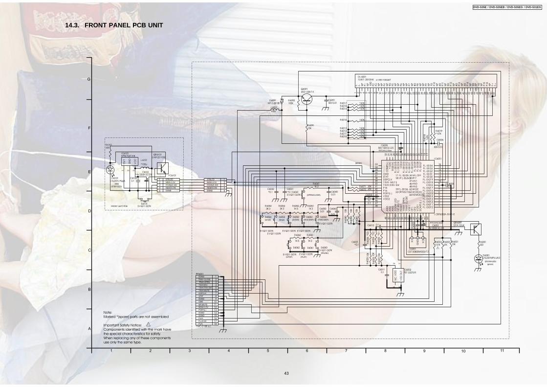
14.3. FRONT PANEL PCB UNIT
R6025
10K
R602110K
R6023
10K
C6002
0.1
C6012 0.1
C60110.1
R6003*47K
R600247K
C6021*0.1
C6003
0.1
S6052
EV Q11 G07K
S6051
EV Q11 G07K
S6050
EV Q11 G07K
S6062
EV Q11 G07K
S6061
EV Q11 G07K
S6060EV Q11 G07K
R6061
1K 2
R60511K 2
R60521K 5
R6062
1K 5
R60532K 2
R60543K 3
R6092100K
S6041EV Q11 G07K
R60411K 2
R6040
10K
R6060
10K
R6050
10KC6060
0.01
C60500.01
C60400.01
TRAYDRV
TRAY/TRV-SW
TRAY-MUTE
C6031
*0.1
C6032
*0.1
NP-MUTE
STAT
DSPCLK
CMD
C60040.1
C609150V 0.01
R6018
*47K
R 6019*47K
STBLEDSTBLED
NSW+3.3VNSW+3.3V
POWER-SWPOWER-SW
REMOCON REMOCON
DGND DGND
OU
T1
GN
D2
VC
C3
I C6101RPM7237-H8
C61020.1
S6101EV Q11 G07K
D6101L NJ201L PQJA
FRONT LEFT PCB
FLH+
FLH-
DGND
NSW+3.3V
FL-24.6V
L 6001
100U
TRAY-OPEN
TRAY-CLOSE
POFF(L)
DGND
DGND
(small) (ZOOM) (RVS-SKIP) (FWD-SKIP)
(STOP) (PLAY)
(PAUSE)
QR6081DT A123JK
D6081L NJ301MPU JAD
(ZOOM-LED)
(green)
(red)
(STBY-LED)
DGND
S6053
EV Q11 G07K
S6054
EV Q11 G07K
(large)
PITCH=2.5mm
PITCH=2.5mm
R6081330
R6101330
C600550V 10[K S]-2.5
C60014V 220[K S]-2.5
(OPEN/CLOSE)
654321
789
101112131415161718
PP6001
T MC-D18P-A1
C6101*4V 220[K S]-2.5
R609110K
Q60912SD1328-T X
C6006
50V 0.01
L 6101
*100u
R6017 *47KR6015 *47KR6014 *47K
R6016 *47K
R6013 *47KR6012 *47KR6011 *47KR6010 *47K
54321
54321
FC6101
XO
GN
DXI
321
X 6001CST S0800MG03-T 2
D6091MT Z J3R3B T A
F-
1
NP
5
10G
6
P2
7
P3
8
NP
9
NP
10
P4
11
NP
12
9G
13
P5
14
NP
15
NP
16
P6
17
NP
18
NP
19
P7
20
NP
21
8G
22
P8
23
NP
24
NP
25
P9
26
NP
27
P10
29
7G
28
NP
30
6G
31
P11
32
NP
33
5G
34
F-
2
NP
3
P1
4
P12
35
NP
36
4G
37
P13
38
NP
39
3G
40
P14
41
NP
42
2G
43
NP
44
1G
45
NP
46
P15
47
P16
48
NP
49
F+
50
F+
51
DL 600110-B T -251GNK
R600110K
QR6101U NR221100L
FL -DGT 01
FL -DGT 12
FL -DGT 23
FL -DGT 34
FL -DGT 45
FL -DGT 56
FL -DGT 67
FL -DGT 78
V DD39
FL -DGT 810
FL -DGT 911
FL -SEG012
FL -SEG113
FL -SEG214
FL -SEG315
FL -SEG416
17
18
19
FL
-SE
G7
20
FL
-SE
G8
21
FL
-SE
G9
22
FL
-SE
G10
23
FL
-SE
G11
24
FL
-SE
G12
25
FL
-SE
G13
26
VD
D4
27
FL
-SE
G14
28
FL
-SE
G15
29
RG
B(H
)30
YC
(H)
31
CO
MP(L
)32
333435
CMD36
ST AT37
DSPCL K38
T RAY -MU T E39
T RAY /DRV -SW40
P1541
P1642
POFF(L )43
V SS244
V DD245464748
AN
349
AN
450
AN
551
ZO
OM
LE
D52
NP-M
UT
E53
RE
SE
T54
TR
AY
OPE
N55
TR
AY
CL
OSE
56
VSS1
57
CF1
58
CF2
59
VD
D1
60
SC
AR
T(L
)61
62
63
64
17 FL -SEG518 V P (-30,6V )
19 FL -SEG633 OFFMU T E
34 NFL OFF35 PF7
46 AN047 AN1
48 AN262 W IDE63 W IDE(H)64 REMOCON
I C6001
L C876332A-51A1-E
(MASK)
or HNV-10SS26T
R6072 47KR6071 30K
VSS
4
VD
D2
NC
3
OU
T1
I C6002PST 3327U R
R6022
*S1
R6024
*S2
R6026
*S3
1
!
Note: Marked *(spare) parts are not assembled
Important Safety Notice:
Components identified with the mark have the special characteristics for safety.When replacing any of these components use only the same type.
F
G
E
D
C
B
A
54321 876 11109
DVD-S35E / DVD-S35EB / DVD-S35EG / DVD-S31EG
43

14.4. DECODER INTERCONNECTION
EXADT[0..15]EXADR[16..20]
NEXWE
TRCDATA0TRCDATA1
NEXCENEXOE
TRCCLK
TRCDATA2TRCDATA3
TRCST
DR
V3
DR
V4
DR
V7
DR
V8
PNRSTSCLOCK
EXTRG0SDATA
D+3.3V
TR
V-S
WS
PD
RV
TR
DR
VF
OD
RV
TR
SD
RV
AD
0
AD
2V
HA
LF
LP
C2
VIN
6V
IN9
VIN
10
VIN
5V
IN4
VIN
3V
IN2
VIN
1V
RE
FH
LP
C1
VIN
8V
IN7
RF
INN
RF
INP
LP
CO
2L
PC
O1
GND
EX
TC
LK
1
S/PDIF
V_GND
YCG/YB/CBR/CR
SR
CK
LR
CK
DM
IXO
UT
DGNDD+1.5V
P[0
..1
5]
D+5V
ST
AT
US
DS
PC
LK
CM
D
RGB(H)YC(H)
WIDE(L)
M9V
-CT
L
FG
FG
EN
B
V_GND1
DV1DV1.sch
EXADT[0..15]EXADR[16..20]NEXWE
TRCDATA0TRCDATA1
NEXCENEXOE
P[0
..1
5]
TRCCLK
TRCDATA2TRCDATA3TRCST
PNRSTSCLOCK
EXTRG0SDATA
D+3.3V
DG
ND
FLASH MEMORYFMEM.sch
AV DECODERFLASH MEMORY
TR
V-S
WS
PD
RV
TR
DR
VF
OD
RV
TR
SD
RV
AD
0
AD
2V
HA
LF
LP
C2
VIN
10
VIN
6V
IN9
VIN
5V
IN4
A+5V
VIN
3V
IN2
LP
C1
VR
EF
HV
IN1
VIN
8V
IN7
RF
INN
RF
INP
LP
CO
2L
PC
O1
D+5V
GND
D+3.3V
HF
MO
NM
UT
E3
GA
IN H
/LM
UT
E1
2
M+9V
M_GND
TRAY/TRVTRAY-MUTE
TRAYDRVTRV-SW
DGND FG
FG
EN
B
DRIVE CONNECTIONPRE.sch
DRIVE CONNECTION
A_GND
D+3.3V
DGND
DM
IXO
UT
EX
TC
LK
1
LAUD_CINCHLAUD L
RC
K
NSW+12V
NSW+16V
RAUD_CINCHRAUD
P[0
..1
5]
SR
CK
SW+5V
NSW+5.6V
GND
V_GND
M+9V
NP_MUTE
AUDIO DACADAC.sch
AUDIO DAC
SW
+5
V
A_GNDV_GND
YC
G/YB/CBR/CR
LA
UD
LA
UD
_C
INC
H
RA
UD
RA
UD
_C
INC
H
NSW+12V
RGB(H)YC(H)
WIDE(L)
D+5V
DGND
S/PDIF
V_GND1
AV INTERFACEIO_AV_nop.Sch
AV INTERFACE
TP
30
02
TP
3003
TP
3001
TP
3005
TP
3007
TP
3009
TP
3011
TP
3013
TP
3017
TP
3018
TP
3019
TP
3020
TP
30
00
TP
3006
R3
00
90
R3
00
10
R3
00
20
R3
00
30
R3
00
40
R3
00
50
R3
00
60
R3
00
70
R3
00
80
6 5 4 3 2 178910
11
12
13
14
15
16
17
18
19
PS2001TWG-P19X-B1
SW
+1
.5V
GN
D
NS
W+
16
V
GN
DD
+5
V
GN
DM
+9
V
GN
D
CM
DD
SP
CL
KS
TA
TU
SN
P_M
UT
E
NS
W+
5.6
V
TR
AY
-MU
TE
TR
AY
TR
V-S
W
TR
AY
DR
VT
RA
Y-C
LO
SE
M9V
-CT
L
GN
D
TP
30
10
K3
00
3
M_GND
GN
DDG
ND
A_GND
V_GND
K3
00
2
*
K20
*(s
chem
atic
only
)
K10
*(s
chem
atic
only
)
!
Note: Marked *(spare) parts are not assembled
Important Safety Notice:Components identified with the mark have the special characteristics for safety.When replacing any of these components use only the same type.
F
G
E
D
C
B
A
54321 876 119 10
DVD-S35E / DVD-S35EB / DVD-S35EG / DVD-S31EG
44

14.5. DECODER PCB (AV DECODER)
C2035
0.0
1
C2034
0.0
1
C2028
0.0
1
C2023
0.0
1
C2019
0.0
1
C2018
0.0
1
C2016
0.0
1
C2014
0.0
1
C2013
0.0
1
C2011
0.0
1
C2010
0.0
1
C2001
0.01
C20020.01
C20080.01
C20040.01
C20050.01
C20060.01
C2007 0.01
C20030.01
C20380.01
C20390.01
C2040
0.01
C2041 0.01
C2020
0.1
C2033
0.1
C2046 0.1C2045 0.1
GND
C20430.1
C20420.1
C2044 0.1
C2022
33P
V IN1VIN2VIN3
VIN8VIN7VIN6VIN5RFINPRFINN
GND shield
V IN4VIN9V IN10L PC1
L PCO1L PC2
L PCO2
R2011
68K
GND shield
C20531500P[K ]
V HAL FV REFH
R2010 1K
AD0
AD2
R20131.3K [0.5%]
R20122K [0.5%]
C20540.1
G/Y
B /CBR/CR
YC
S/PDIF
DMIX OU T
SRCKL RCK
C2061*0.1
C2062
*0.1
C2063
*0.1
C2069
*22P
R2014 100
RA
2009
82 X
4
RA
2008
82 X
4
RA
2007
82 X
4
RA
2005
82 X
4
RA2006
82 X
4
RA
2003
82 X
4
RA
2004
82 X
4
MDQ0
MDQ1
MDQ2
MDQ3
MD
Q4
MD
Q5
MD
Q6
MD
Q7
MD
Q8
MD
Q9
MD
Q10
MD
Q1
1
MDQ12
MDQ13
MDQ14
MDQ15
MD
Q16
MD
Q1
7
MD
Q1
8
MD
Q1
9
MDQ20
MDQ21
MDQ22MDQ23MDQ24
MDQ25
MDQ26
MDQ27
MD
Q28
MD
Q2
9
MD
Q3
0
MD
Q3
1
MA
0
MA
1
MA
2
MA
3M
A4
MA
5
MA
6
MA
7
MA
8
MA
9
MA
10
MA
11
C2084
0.0
1
C2078
0.0
1
C2059
0.0
1
C2055
0.0
1
C2049
0.01
C2052
0.01
C2058
0.01
C2060
0.0
1
C2072
0.01
C2080
0.01
C2085
0.01
C2086
0.01
MD
Q0
MD
Q1
MD
Q2
MD
Q3
MD
Q4
MD
Q5
MD
Q6
MD
Q7
MD
Q8
MD
Q9
MD
Q10
MD
Q1
1M
DQ
12
MD
Q1
3M
DQ
14
MD
Q1
5
MD
Q1
6
MD
Q1
7M
DQ
18
MD
Q1
9M
DQ
20
MD
Q2
1M
DQ
22
MD
Q2
3M
DQ
24
MD
Q2
5M
DQ
26
MD
Q2
7M
DQ
28
MD
Q2
9M
DQ
30
MD
Q3
1
MA
0M
A1
MA
2M
A3
MA
4M
A5
MA
6M
A7
MA
8M
A9
MA
10
MA
11
DQ
M0
DQ
M1
DQ
M2
DQ
M3
BS
0BS1
NW
E
NC
SN
RA
SN
CA
S
NC
AS
NRA
SN
CS
NW
E
DQ
M0
DQ
M1
DQ
M2
DQ
M3
BS
0
BS1
EX ADR16
EX ADR17
EX ADR18
EX ADR19
EX ADR20EX ADR[16..20]
EXADR[16..20]
EX ADT 0
EX ADT 1
EX ADT 2
EX ADT 3
EX ADT 4
EX ADT 5
EX ADT 6
EX ADT 7
EX ADT 8
EX ADT 9
EX ADT 10
EX ADT 11
EX ADT 12
EX ADT 13
EX ADT 14
EX ADT 15
EX ADT [0..15]EX ADT [0..15]
NEX WE
NEX CE
NEX OE
P8P9P10
P13
P[0..15]P[0..15]
KMODESCLSDA
P0
SBT1SBO1
PNRST
DRV 4
DRV7DRV8
T RSDRVSPDRV
DRV 3
TR
SD
RV
T RSDRVSPDRV
SPD
RV
DR
V3
DRV4
DRV7
DRV8
DRV 3
DRV 4
DRV 7DRV 8
TR
V-S
W
T RV -SWTRV-SW
R2033 1K R2036
*1K
R2035
*1K
R2034 1K
SCL OCKEX T RG0SDAT A
T RCCL KT RCDAT A0TRCDATA1TRCDATA2TRCDATA3
T RCST
R2037
33DGND shield
L 2005
10U /155MA
C2073
6V 100(K A)
DGND
L 2003
ERJ6GEY 0R00V
V _GND
C20826V 100(K A)
L 2001
10U /155MAL 2002
10U /155MA
C2071
6V 100(K A)C20706V 100(K A)
GND
C65660.1
L B 6561B K 1608HM601-T
L B 6564B K 1608HM601-T
L B 6562J0JCC0000062
L B 6563*B K 1608HS121-T L B 6567
B K 1608HM601-T
R656310K
R6565 47
C65670.1
C65640.1
L B 6565B K 1608HS121-T
C2099
0.1
X 650136.864MHZ
C650315P
C6505*12p
P5P6
CLKSEL
33MHZ
54MHZ
SC
LK
SCLK
VGND shield
EX T CL K 1
C209810V 10 - [T ]
D+5V
D+3.3V
AMUTE
STBDAC
R6561*10K
R656410
DQ
713
NC
14
VC
C15
DQ
M0
16
WE
17
CA
S18
RA
S19
CS
20
NC
21
BS
022
BS
123
A10/A
P24
A0
25
A1
26
A2
27
DQ
M2
28
VC
C29
NC
30
DQ
16
31
VS
SQ
32
DQ
17
33
DQ
18
34
VC
CQ
35
DQ
19
36
DQ
20
37
VS
SQ
38
DQ
21
39
DQ
22
40
VC
CQ
41
DQ
23
42
VC
C43
VC
C1
DQ
02
VC
CQ
3
DQ
14
DQ
25
VS
SQ
6
DQ
37
DQ
48
VC
CQ
9
DQ
510
DQ
611
VS
SQ
12
DQ
31
56
NC
57
VS
S58
DQ
M3
59
A3
60
A4
61
A5
62
A6
63
A7
64
A8
65
A9
66
CK
E67
CL
K68
NC
69
NC
70
DQ
M1
71
VS
S72
NC
73
DQ
874
DQ
976
DQ
10
77
VSSQ
78
DQ
1179
DQ
12
80
VC
CQ
81
DQ
13
82
DQ
14
83
VSSQ
84
DQ
15
85
VS
S86
VS
S44
DQ
24
45
VSSQ
46
DQ
25
47
DQ
26
48
VC
CQ
49
DQ
27
50
DQ
28
51
VSSQ
52
DQ
29
53
DQ
30
54
VC
CQ
55
VC
CQ
75
IC2002MT 48L C4M32B 2T G
C20871000p
C20882200p
V DD11
V SS12
MO13
MO24
V DD25
V SS26
X T I7
X T O8
AO19
AO210
V SS311
V DD312
SO113
FSEL14
SO215
CE16
IC6561
B U 2286FV
V CC5
GND3
OU T4
M/R1
SU B2
IC2003
PST 596JNR
DSPCL KST AT U S
CMD
R2095
10K
R2096
10K
R2097
10K
P15
C2047220P
R2009*510 0.5%
R2008 30K 0.5%
C2031
5600P[K
]C
2030
0.0
18u[K
]
T P6563
TP6564
TP6565
TP6561
R2016 8K 2
R2018 8K 2C2096820P
C20951000P
R2015 0
R2017 0
FODRV
TRDRV
GND
GND
R2091 15K
R2093 15K
C2093
1000PC2083
4700P[K ]
R2044 7K 5
R2042 7K 5
R2043 0
R2041 0
R2090 10K
R2002
RGB (H)
Y C(H)WIDE(L )
M9V
-CT
LM9V -CT LM9V-CTL
C2092
*
C20970.1
T P2001
C20500.01u[K ]C20510.1u[K ]
C2027
0.0
1u[K
]
C2021
0.0
33u[K
]
C2064
0.1
u[K
]
C2065
0.1
u[K
]
C2089100P
D+1.5V
C2090*10V 10 - [T ]
C2079*6V 100(K A)
C2017
0.1
C2015
0.1
C2012
0.1
C2009
0.1
R20014K 7
C2066
0.1
RA
2012
82 X
2
R200333
R6562220
R2099
47K
R2098*
C20361u[K ]
C2037
1u[K ]
C20481u[K ]
L 6561
NL FV 25T -220K
L 6562NL FV 25T -220K
GN
D5
IN1
ON/OFF2
OU T3
NC4
IC2005PQ3DZ 13U
C2032
0.1u[K ]
R20050
FG
EN
B
FGENBFGENB
FG
V DD331
MDQ112
MDQ33
V SS4
MDQ125
MDQ26
V DD337
MDQ138
MDQ19
MDQ1410
V SS11
MDQ012
MDQ1513
V DD3314
V DD1515
V SS16
EX ADR2017
NEX WE18
EX ADT 019
EX ADT 420
EX ADT 821
EX ADT 1222
V DD3323
V SS24
EX ADR1625
EX ADR1826
EX ADT 1427
EX ADT 1028
V DD3329
V SS30
EX ADT 631
EX ADT 232
NEX CE33
EX ADT 134
EX ADT 535
EX ADT 936
EX ADT 1337
EX ADR1738
EX ADR1939
EX ADT 1540
EX ADT 1141
V DD3342
V SS43
EX ADT 744
EX ADT 345
NEX OE46
P1547
P1448
P1349
P1250
P1151
P1052
P953
P854
P755
V DD356
MMOD57
V SS58
P659
P560
P461
P362
P263
P164
P0
65
FG
66
VD
D15
67
NR
ST
68
VSS
69
DR
V0
70
DR
V1
71
DR
V2
72
DR
V3
73
DR
V4
74
DR
V5
75
DR
V6
76
DR
V7
77
DR
V8
78
VD
D33
79
VSS
80
SC
LO
CK
81
EX
TR
G0
82
SD
ATA
83
EX
TR
G1
84
TR
CC
LK
85
TR
CD
ATA
086
TR
CD
ATA
187
TR
CD
ATA
288
TR
CD
ATA
389
TR
CST
90
VD
D33
91
OSC
I92
VSS
93
MO
NI7
94
MO
NI6
95
MO
NI5
96
MO
NI4
97
VD
D15
98
VSS
99
MO
NI3
100
MO
NI2
101
MO
NI1
102
MO
NI0
103
AV
DD
D104
PL
FIL
1105
AV
SS
D106
PL
FIL
2107
VR
EFA
108
VR
EFB
109
VR
EFC
110
VC
011
1
RE
SI
112
AN
AM
ON
I11
3
PO
FLT
114
CD
ATA
115
CC
APA
116
CG
D11
7
AV
DD
C11
8
AV
SSC
119
RFIN
N120
RFIN
P121
VIN
5122
VIN
6123
VIN
7124
VIN
8125
VIN
1126
VIN
2127
VIN
3128
V IN4129
V IN9130
V IN10131
L PC1132
L PCO1133
L PC2134
L PCO2135
V REFH136
V HAL F137
AV SSB138
CT K C139
CSL FLT140
CWB L OU T141
CWB L IN142
V COF143
RV I144
AV DDB145
AD2146
AD1147
AD0148
AV DDA149
DAC1150
AV SSA151
DAC0152
AV DDE153
IREF2154
AV SSE155
COMP1156
AV DDF157
DAC1OU T158
AV SSF159
DAC2OU T160
DAC3OU T161
V REF162
DAC4OU T163
DAC5OU T164
AV DDG165
IREF1166
AV SSG167
COMP2168
V SS169
B ECL K170
V DD33171
EX T CK172
PHCOMPO173
L RCK174
SRCK175
ADOU T 3176
V SS177
ADOU T 2178
ADOU T 1179
ADOU T 0180
IECOU T181
V DD33182
V SS183
MDQ24184
MDQ23185
V DD15186
MDQ22187
MDQ25188
V DD33189
MDQ26190
MDQ21191
MDQ27192
MD
Q20
193
VS
S194
VD
D33
195
MQ
D28
196
MQ
D19
197
VS
S198
MQ
D29
199
MQ
D18
200
MQ
D30
201
VD
D33
202
MQ
D17
203
MQ
D31
204
MQ
D16
205
VS
S206
DQ
M3
207
DQ
M2
208
VD
D33
209
MA
3210
VS
S211
MA
4212
VD
D15
213
MA
2214
VS
S215
MA
5216
MA
1217
VD
D33
218
MA
6219
MA
0220
VS
S221
VD
D15
222
MC
KI
223
VS
S224
MC
K225
VD
D33
226
MA
7227
MA
10
228
MA
8229
VS
S230
MA
11231
NW
E232
VD
D33
233
BA
0234
MA
9235
VS
S236
BA
1237
NC
SM
238
NRA
S239
VD
D33
240
VS
S241
NC
AS
242
DQ
M0
243
VD
D15
244
VS
S245
DQ
M1
246
MD
Q7
247
VS
S248
MD
Q8
249
VD
D33
250
MD
Q6
251
MD
Q9
252
MD
Q5
253
VS
S254
MD
Q10
255
MD
Q4
256
IC3001
MN2DS0002AP1
C2029
180p
C205610V 1
C205710V 1
C2024
0.1
C2026
0.1
C2025
0.1
C6561
6,3V 330[K A ]
C6563
6V 330[K A]
C2067*100P
shie
ld w
ith D
GN
D
R2019*0
R200715K (0.5%)
R2004
3.9
K[1
%]
RA2002
82 X 4
RA2001
82 X 4
RA2011
82 X 4
RA2010
82 X 4
R2020
33
K 2001
V _GND1V_GND1
R202210K
C20812200P[K ]
R200615K (0.5%)
R2021 82R2023 82
!
Note: Marked *(spare) parts are not assembled
Important Safety Notice:Components identified with the mark have the special characteristics for safety.When replacing any of these components use only the same type.
Audio Signal Path
Video Signal Path
F
G
E
D
C
B
A
54321 876 119 10
DVD-S35E / DVD-S35EB / DVD-S35EG / DVD-S31EG
45
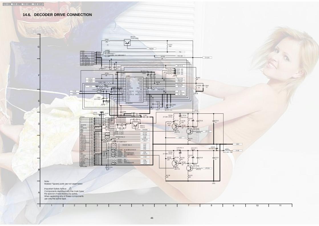
14.6. DECODER DRIVE CONNECTION
B IAS11
V IN12
V IN23
OPIN+4
OPIN-5
OPOU T6
GND(Pre)7
V CC(ch1.2)8
MU T 129
GND(ch1.2)10
MU T E420
L DIN24
B IAS225
T R IN26
MU T E327
L DCNT28
V O4+15
V O4-16
GND(ch3.4)19
V O1-13
V O1+14
V IN323
PREV CC22
V CC(ch3.4)21
V O2-11
V O2+12
V O3+17
V O3-18
FIN FIN
IC2501
B A5833FM
V HAL FT RDRVFODRV
AD0
D+5V
DGND
R2512 82K
R2513 82K
R2515
100
C2503
16V 22 - K A
MU T E12
T RAY /T RVMU T E3
T RSDRV
T RAY DRVSPDRV
M+9V
M_GNDT RAY -MU T E
L B 2521 B K 1608HM601-T
GND(FG2)T RV -SW
SPD-MOT OR+SPD-MOT OR-
T RV -MOT OR+T RV -MOT OR-
T RV -SWR2102
47KD+3.3V
T +F+F-T -3.3V HFMGNDL D+(DV D)GNDGNDRFPRFNF1(DV D)F2(DV D)GAIN H/LPIN(DV D)V REF2.2(DV D)T A (DV D)T D(DV D)T C(DV D)T B (DV D)V CC5VFE1GNDL D+(CD)T 1(CD)V REF2.2(CD)FE2(CD)T 2(CD)PIN(CD)GND
L B 5111 MCR03EZHJ000L B 5110 MCR03EZHJ000L B 5109 MCR03EZHJ000L B 5122 MCR03EZHJ000L B 5107
B K 1608HM601-T
L B 5106B K 1608HM601-T
L B 5102 B K 1608HM601-T
L B 5101 MCR03EZHJ000
L B 5103 MCR03EZHJ000
D5111 MA728-T X
K 5112 *
QR5111U N2121
18273645
RA5101 56 x 4
RA5103 56 x 2
RA5102 56 x 2
R51064K 7
R5105 1K
L B 5105 B K 1608HS121-T
R5103 2K 2
R5104 56
R5102 56R5101 2K 2
K 5111*
HFMON
RFINPRFINNV IN7VIN8
GAIN H/LL PC1
V IN1VIN2VIN3VIN4
VIN5V REFH
V IN9
VIN6V IN10L PC2
K 2501K2502 *
K 2503
Q51322SB 1115
R5134
56
R51352R2
C5134
6,3V 47-K A
R51310
R5137
47K
L PCO1
Q51222SB 1115
R5124
56
R51252R2
C5124
6,3V 47-K A
R51210
R5127
47K
L PCO2
R512822K
A+5V
GND
GND
AD2
R513627 0.5W [1812]
R512627 0.5W [1812]
D2512 *
D2511 *
C5133*
C5123*
C2506
0.1
C25050.1
C51210.1
C51310.1
C2512
0.1
C25080.1
C25210.1
C25220.1
C51040.1
C2507
0.1
C25040.1
C25110.1
C5102
0.1
C51030.1
Q5121
2SD1819A
Q5131
2SD1819A
L B 5133 B L M18PG121SN1D
L B 5104 B L M18PG121SN1D
C250216V 47 - K A
C5141 0.1u[K ]C5142 0.1u[K ]
R2532
1K
C25310.1
R25312K
R2516 47KR2517 47KR2518 47KR2519 47K
C512016V 47[K A]
C51226.3V 4.7[T ]
C51326.3V 4.7[T ]
C25016,3V 330[K A ]
151413121110
987654321
16
3029282726252423222120191817
FP5101
52976-3092
T P5101TP5102TP5103TP5104TP5105
TP5106
TP5107TP5108TP5109TP5110TP5111TP5112TP5113TP5114TP5115TP5116TP5117TP5118TP5119
TP5120TP5121TP5122TP5123TP5124TP5125TP5126
TP2501TP2502TP2503TP2504TP2505TP2506
TP5127
TP5128
C51016V 47(K S)
R51221K
R51321K
R5123330
R5133330
FG3FG1
R2511
15K
T P2507TP2508
L B 2522
*B K 1608HM601-T
FGENB
FG
R2101*82K
QR2101*U N511M00L
R2514 15K
C25090.1
R2501 6R8[0805]
654321
78
FP2501
52793-0890 (MOL EX )
L 5121
NL FV 25T -100K
R2521
*220
1
!
Note: Marked *(spare) parts are not assembled
Important Safety Notice:Components identified with the mark have the special characteristics for safety.When replacing any of these components use only the same type.
F
G
E
D
C
B
A
54321 8 10976 11
DVD-S35E / DVD-S35EB / DVD-S35EG / DVD-S31EG
46

14.7. DECODER FLASH MEMORY
EXADT[0..15]
EXADT 15EXADT 14EXADT 13EXADT 12EXADT 11EXADT 10EXADT 9EXADT 8
EXADT 7EXADT 6EXADT 5
EXADT 3EXADT 2EXADT 1EXADT 0
EXADT 15EXADT 7EXADT 14EXADT 6EXADT 13EXADT 5EXADT 12EXADT 4
EXADT 11EXADT 3EXADT 10EXADT 2EXADT 9EXADT 1EXADT 8EXADT 0
FADR15FADR14FADR13FADR12FADR11FADR10FADR9FADR8
FADR7FADR6FADR5FADR4FADR3FADR2FADR1FADR0
FADR[0..15]
FADR15FADR14FADR13FADR12FADR11FADR10FADR9FADR8EXADR19EXADR20
EXADR18EXADR17
FADR7FADR6FADR5FADR4FADR3FADR2FADR1
EXADR16
FADR0
EXADR[16..20]NEXWENEXCENEXOE
PNRST
D+3.3V
DGND
R6302
4K7
R6303
4K7
R6301100
T RCCL K
EX T RG0
T RCDATA0
SDATA
T RCDATA1
TRCDATA2
TRCDATA3
T RCST
GNDTRCCLKGND
P10
GNDTRCDATA[0]GNDTRCDATA[1]GNDTRCDATA[2]GNDTRCDATA[3]GNDTRCSTGND
P[0..15]
P9P8
S CLS DA
KMODE
SCLOCK
EXADT 4
DGND
A151
A142
A133
A124
A115
A106
A97
A88
A199
NC(A20)10
/WE11
RDY, /B SY15
A1816
A1717
DQ10 34
DQ4 38DQ12 39DQ5 40
DQ6 42
DQ13 41
DQ14 43DQ7 44DQ15A-1 45V SS 46/B Y T E 47A16 48
A718
A619
A520 DQ0 29DQ8 30DQ1 31DQ9 32DQ2 33
/RESET12
NC13
NC(WP)14
VDD 37
DQ11 36
DQ3 35
A421
A322
A223
A124
/OE 28
V SS 27
/CE 26
A0 25
IC6303
M29W160DT (M29W320DT )
/OE1
D02
D13
D24
D35
D46
D57
D68
D79
GND10 L E 11Q7 12
Q5 14
Q6 13
Q4 15Q3 16Q2 17Q1 18Q0 19VCC 20IC6302
T C74VHC573FT (EL )
/OE1
D02
D13
D24
D35
D46
D57
D68
D79
GND10 L E 11Q7 12
Q5 14
Q6 13
Q4 15Q3 16Q2 17Q1 18Q0 19VCC 20IC6301
T C74VHC573FT (EL )
DGND
987654321
10
PS6301
10FLT -SM1-T B
P15
T P6301TP6302
TP6303
TP6304
TP6305TP6306TP6307
C63030.1
C63040.1
C6301 0.1
C63050.1
C6302 0.1
987654321
1011121314
PS6302
14FLT -SM1-T B
R6304 4K 7
R6305 4K 7
L B 6301
R6306 10K
R6307 10K
DGND
SCLOCK
DGND
PNRST
KMODE
EXT RG0DGND
S DAT A
DGND
D+3.3V
A01
A12
A23
GND4 SDA 5SCL 6WP 7VCC 8IC6304
M24C16-WMN6T
!
Note: Marked *(spare) parts are not assembled
Important Safety Notice:Components identified with the mark have the special characteristics for safety.When replacing any of these components use only the same type.
F
G
E
D
C
B
A
54321 8 9 1076 11
no service partmust replace PCB Unit
DVD-S35E / DVD-S35EB / DVD-S35EG / DVD-S31EG
47

14.8. DECODER AV INTERFACE
WIDE(L )
NSW +12V
SW +5V
V _GND1
L AUD
S/PDI F
D+5V
DGND
G/Y
RGB (H)
RAUD
Y C(H)
C38110.1
R3833
75
R3829
220
R3828
220
R3834
470[D]
L 3809
*470uL 3808
*470u
C3825
6V 47(K A)
R3831
220
R3830220
L AU D_CINCHRAU D_CINCH
L 3801
22U
C3829*100P
R3805
47K
R3806
47K
A_GND
SW1
OU T2
V CC3
IN24
GND5
IN16
IC3802
MM1505X NRE
C3801
0.01
C3809
0.1
C38100.1
C38286V 100[K A]
C3835 6V 100[K A ]
C3836 6V 100[K A ]
Q38032SB 709A
Q38042SB 709A
QR3801U N5111
QR3802U N5213
Q38012SD601A
Q38022SB 709A
D3801 MA111-T X
R3804
10K
R3839
22K
R383710K (G)
R383822K
R3841
18K [G]
C38080.1
R3840
12K [G]
L 3807
22U /280MA
C38036V 100(K A )
MU T E1
INA2
GND3
INB4
GND5
NC6
INC7
GND8
OU T C29
OU T C110
NC11
OU T B 212
OU T B 113
OUT A214
OUT A115
V CC16
IC3801
B A7660FS-E2
C38060.1
R38172K 2
R38182K 2
R38192K 2
C38220.1
MU
TE
(H)
C3812
ERJ3GEY 0R00V
L 3810
*10U /155MAC3813
*22P
B /CB
R3809*150[0.5%]
C
Y
R/CR
R3807*150[0.5%]
N
C3826
6V 47(N)
R3810*75[0.5%]
R3812*75[0.5%]
R381575[0.5%]
R381675[0.5%]
QR3803*U N5213
R384510K
R3832
75
C383416V 22(K A )
C3802
0.01u[K ]
C3824
*100P
R38013K 3[0.5%]
R38023K 3[0.5%]
R384275[0.5%]
R384375[0.5%]
C3843 6V 1000(FW )
C3840 6V 1000(FW )
C3804 6,3V 330[K A ]
C3805 6,3V 330[K A ]
R3846
0
L B 3801
*B K 1608HM601-T
L B 3802
*B K 1608HM601-T
L B 3803
*B K 1608HM601-T
L B 3804
*B K 1608HM601-T
V in3
V cc2
GND1
IC3804
T OT X 179
L 3802
*5.6u
L 3803
*5.6u
L 3804
*5.6u
R3811*75[0.5%]
V CC11
CIN2
MU T E13
V IN14
Y C-MIX5
Y IN6
B IAS7
GND18
NC9
GND110
NC11
CY IN12
CL P13
MU T E215
CRIN16
GND217
CB IN14
CRSAG18
CROU T19
GND220
CB SAG21
CB OU T22
GND223
CY SAG24
GND226
Y SAG27
Y OU T28
GND229
V SAG30
V OU T31
GND232
COU T33
V CC34
CY OU T25
IC3803
MM1567B JB E
SW1
OU T2
V CC3
IN24
GND5
IN16
IC3805
*MM1507X NREK 3801R3803
*1M
R3813*1M
K 3802*
K 3803
1 3
5 7
91
11
31
51
71
92
12
01
81
61
41
21
0 8
6 4
2 0
0JK 3801
12012 (GRAVAL OS)or YKF41-5040 (JALCO)
R3820
75[0.5%]
R3821
75[0.5%]
R3822
75[0.5%]
R3823
75[0.5%]
R3824
75[0.5%]
R3826
75[0.5%]
R3825
75[0.5%]
R3827
75[0.5%]
C383216V 22(SW )
C383316V 22(SW )
C383116V 22(SW )
C3821
*16V 1[Z ]
C3820
*16V 1[Z ]
C3807 *0.1
R3808*150[0.5%]
C3814*68p
C3817*68p
C3815*68p
C3818*68p
C3816*68p
C3819*68p
QR3804U N5213
R38144K 7
V _GND1V _GND
C3830*12P
YC
RC
B
3
CV
BS
2
1
6
5
4
LR
9
8
7
rw
rb
ygn
JK 3802
MSD-246V -70NI L F
K 3804*
K 3805*
K 3806*
!
Note: Marked *(spare) parts are not assembled
Important Safety Notice:Components identified with the mark have the special characteristics for safety.When replacing any of these components use only the same type.
Audio Signal Path
Video Signal Path
F
G
E
D
C
B
A
54321 8 9 1076 11
DVD-S35E / DVD-S35EB / DVD-S35EG / DVD-S31EG
48
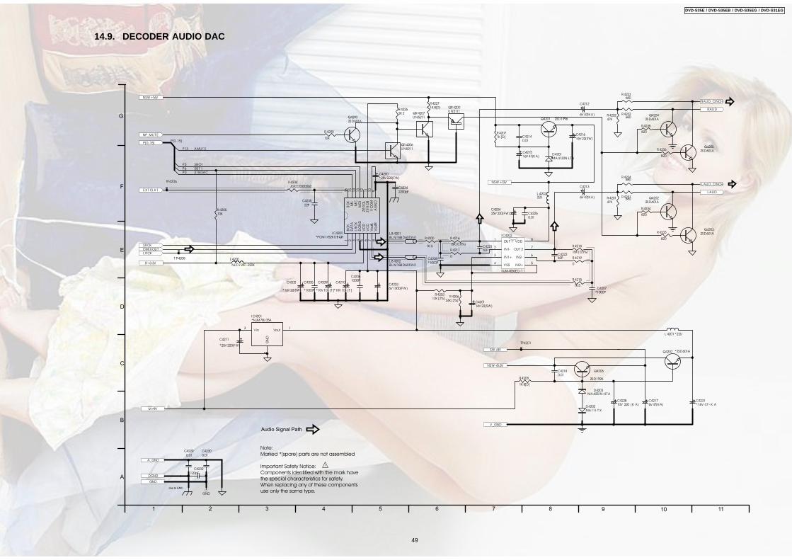
14.9. DECODER AUDIO DAC
SRCKDMIX OU T
EX T CL K 1
L RCK
NSW +12V
A_GND
DGND
D+3.3V
C42260.01
RAU D
NSW +16VR4223
680
QR4206U N5211
R42262K 2 QR4207
U N5211
QR4200U N5111
Q42052SD601AR4236
820
Q42042SD601A
R4232680
R4235
820
RAU D_CINCH
R420247K
L 4201 *22U
L 420222U
C4205
*1000P
C42061000P
C4207*1000P
C4208*1000P
C4209
*10V 10 - [T ]
C4210
*10V 10 - [T ]
C4229
0.01
BC
K1
DA
TA
2
LR
CK
3
DG
ND
4M
DI
13
MC
14
ML
15
SC
K16
ZE
RO
L12
ZE
RO
R11
VC
OM
10
AG
ND
9
VD
D5
VC
C6
VoutL
7
VoutR
8
I C4200*PCM1752K DB QR
L AU D
R4224680
Q42032SD601AR4233
820
Q42022SD601A
R4231680
R4234
820
L AU D_CINCH
R420147K
P[0..15]
P5P6
SB O1SB T 1
Q4201 2SD1996
D4201MA4130N-LT A
C421516V 47(K A)
R42071K [D]
SW +5V
NSW+5.6V
Q4206
2SD1996
C42180.01
Q4207 *2SD601A
C422810V 220 (K A )
D4202MA111-T X
P0 ST B DAC
P13 AMU T E
P[0..15]
GND
GND
C4230
0.01
M+9V
NP_MU T E
Q42902SD601A
R4290
10K
V _GND
C42140.01
C42342200pF
T P4208
TP4201
TP4206
C4231*16V 47 - K A
R4204J0JCC0000062
R4208
1K 8[D]
R42271K 8[D]
C4200*25V 220(FW )
C42036V 1000(FW )
C420425V 220(FW )
Vout1
V in3
GN
D2
IC4201*NJM78L 05A
C4211
*25V 220(FW )
L B 4202B L M18B D601SN1
L B 4201B L M18B D601SN1
C42176V 47(K A)
C4212
6V 47(K A)
C4213
6V 47(K A)
OU T 11
IN1-2
IN1+3
V SS4
IN2+5
IN2-6
OU T 27
V DD8
IC4202
NJM4580ED-T 1
L 4200
NL FV 25T -220K
C420116V 22(SW )
C4202
*16V 22(SW )
C421616V 22(SW )
C4235
22P
R420510K
due to EMC
C4232
120pF
R4217
0 R4219
0
R4200
7K 5
R4215
7K 5
R4216
15K (0.5%)R4218
15K (0.5%)
C422182P
C422282P
D4203MA4051N-HT A
R420312K [2%]
R420624K [2%]
!
Note: Marked *(spare) parts are not assembled
Important Safety Notice:Components identified with the mark have the special characteristics for safety.When replacing any of these components use only the same type.
Audio Signal Path
F
G
E
D
C
B
A
54321 8 9 1076 11
DVD-S35E / DVD-S35EB / DVD-S35EG / DVD-S31EG
49
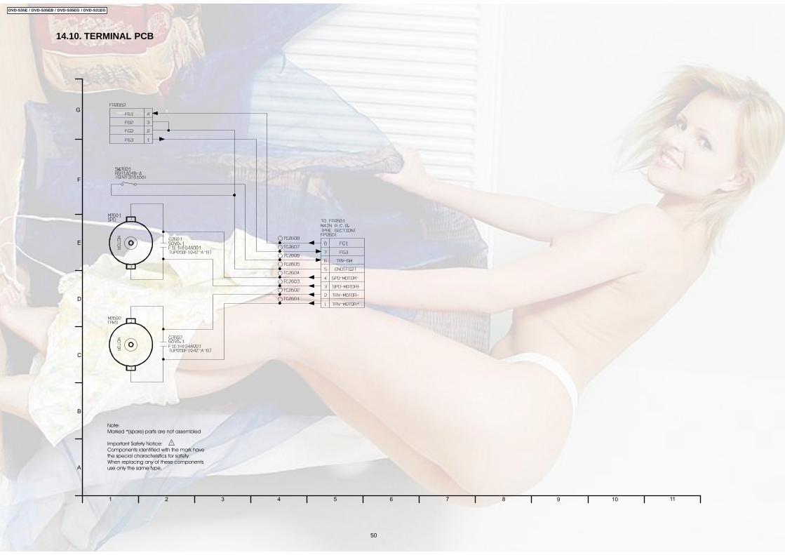
14.10. TERMINAL PCB
!
Note: Marked *(spare) parts are not assembled
Important Safety Notice:Components identified with the mark have the special characteristics for safety.When replacing any of these components use only the same type.
F
G
E
D
C
B
A
54321 8 976 1110
DVD-S35E / DVD-S35EB / DVD-S35EG / DVD-S31EG
50

15 PRINT CIRCUIT BOARD15.1. Decoder PCB Unit
DVD-S35E / DVD-S35EB / DVD-S35EG / DVD-S31EG
51
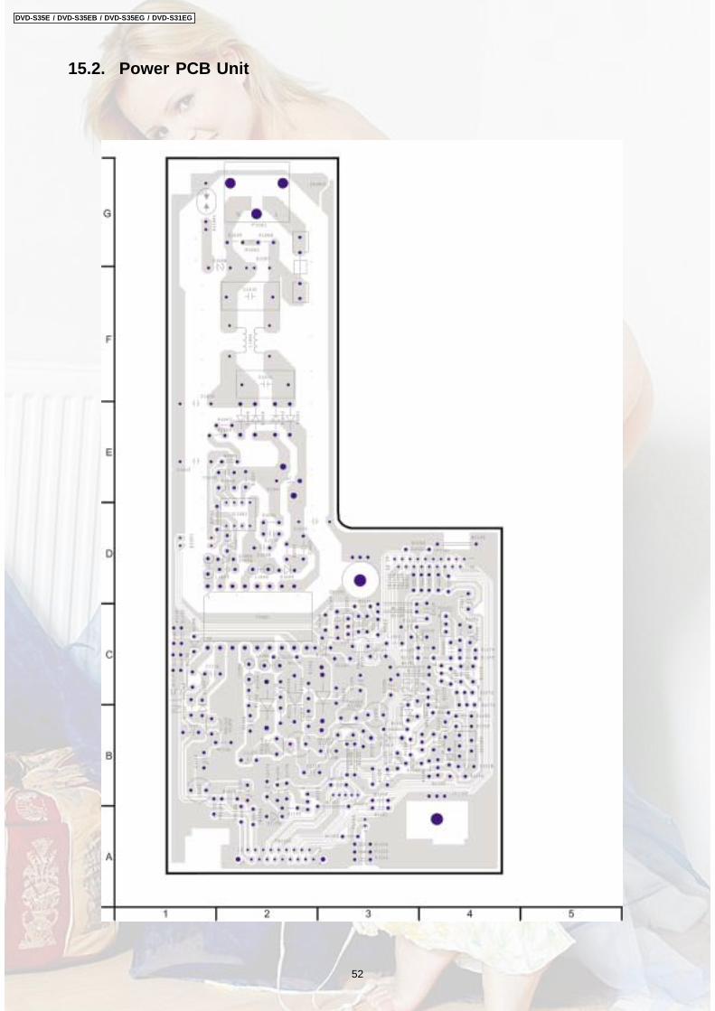
15.2. Power PCB Unit
DVD-S35E / DVD-S35EB / DVD-S35EG / DVD-S31EG
52
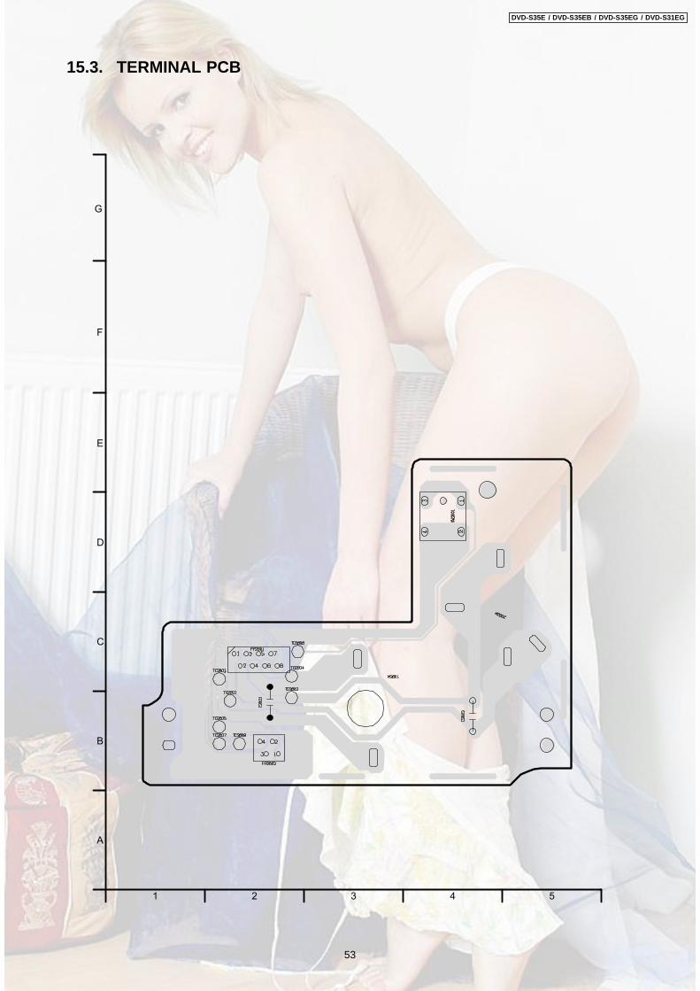
15.3. TERMINAL PCB
F
G
E
D
C
B
A
54321
DVD-S35E / DVD-S35EB / DVD-S35EG / DVD-S31EG
53

15.4. Front PCB Unit
DVD-S35E / DVD-S35EB / DVD-S35EG / DVD-S31EG
54
16 EXPLODED VIEWS16.1. Casing Parts& Mechanism Section Exploded View
55
DVD-S35E / DVD-S35EB / DVD-S35EG / DVD-S31EG

16.2. Mechanism Section Exploded View
56
DVD-S35E / DVD-S35EB / DVD-S35EG / DVD-S31EG
16.3. Packing& Accessories Section Exploded View
57
DVD-S35E / DVD-S35EB / DVD-S35EG / DVD-S31EG
17 REPLACEMENT PARTSLIST
Notes:*Important safety notice:Components identified by mark have specialcharacteristics important for safety.Furthermore, special parts which have purposes of fire-retardant (resistors), high-quality sound (capacitors), low-noise (resistors), etc. are used.When replacing any of components, be sure to use onlymanufactures specified parts shown in the parts list.*Warning: This product uses a laser diode. Refer to cautionstatements.*ACHTUNG: Die Lasereinheit nicht zerlegen. DieLasereinheit darf nur gegen eine vom Herstellerspezifizierte Einheit ausgetauscht werden.*Capacity values are in microfarads (µF) unless specifiedotherwise, P=Pico-farads (pF), F=Farads (F).*Resistance values are in ohms, unless specified otherwise,1K=1,000 (OHM), 1M=1,000k (OHM).*The marking (RTL) indicates the retention time is limitedfor this item. After the discontinuation of this assembly inproduction, it will no longer be available.
Ref.No.
Part No. Part Name Pcs Remarks
Casing Parts
1 RYPD00011A-S Front Panel Assy 1 DVD-S35E-SDVD-S35EB-SDVD-S35EG-S
1 RYPD00011B-K Front Panel Assy 1 DVD-S35E-KDVD-S35EB-KDVD-S35EG-K
1 RYPD00012A-S Front Panel Assy 1 DVD-S31EG-S
1 RYPD00012B-K Front Panel Assy 1 DVD-S31EG-K
2 RKWD0003-R FL Window 1
3 VGB0560 Brand Badge Panas. 1
4 RYFD0001-S Tray Ornament Unit 1 DVD-S35E-SDVD-S35EB-SDVD-S35EG-SDVD-S31EG-S
4 RYFD0001-K Tray Ornament Unit 1 DVD-S35E-KDVD-S35EB-KDVD-S35EG-KDVD-S31EG-K
5 RMAD0003 Front support angle 1
6 XTBS26+10J Screw 8 Front PCBUnit
7 RKMD0003-S Topcase 1 DVD-S35E-SDVD-S35EB-SDVD-S35EG-SDVD-S31EG-S
7 RKMD0003-K Topcase 1 DVD-S35E-KDVD-S35EB-KDVD-S35EG-KDVD-S31EG-K
8 VHD1094 Screw 2 DVD-S35E-SDVD-S35EB-SDVD-S35EG-SDVD-S31EG-S
8 VHD1041 Screw 2 DVD-S35E-KDVD-S35EB-KDVD-S35EG-KDVD-S31EG-K
9 XTBS3+8JFZ1 Screw 3 Topcase rear
10 RXKD0005 Chassis Unit 1
11 RGKD0008-K Chassis ornament 2
12 RKA0132-K Set Leg Unit 2
13 XTB3+6JFZ Screw 2 Set Leg Unit
14 RKA0137-K Rubber Cushion 2
Ref.No.
Part No. Part Name Pcs Remarks
15 RGRD0003A-1A Rear Panel 1 DVD-S35E-SDVD-S35E-KDVD-S35EB-SDVD-S35EB-KDVD-S35EG-SDVD-S35EG-K
15 RGRD0003A-1B Rear Panel 1 DVD-S31EG-SDVD-S31EG-K
16 XTBS26+8J Screw 7 Rear Panel
17 RHD30102 Screw 4 MechaChassis
18 REPD0006A Front PCB Unit 1 DVD-S35E-SDVD-S35E-KDVD-S35EB-SDVD-S35EB-KDVD-S35EG-SDVD-S35EG-K
18 REPD0006B Front PCB Unit 1 DVD-S31EG-SDVD-S31EG-K
19 XTBS3+8JFZ1 Screw 2 Power Unit
20 REXD0001 2PIN Cable 1
21 RHD30090 Screw 1 Decoder Unit
22 RHDC0002 Screw 1 Mecha-Decoder
23 REYD0007 8PIN FFC 1
24 REPD0005A Decoder PCB 1 (RTL)
25 REPD0007A Power PCB 1 (RTL)
Mecha Chassis Unit
101 RXQ1016A Spindle Motor Assy 1
102 RMR1323-K Middle Chassis 1
103 RMS0712 Fixed Pin 2
106 REP3501A-C Terminal PCB 1 (RTL)
107 XTN2+6G Screw 1
108 RMG0545-A1 Floating Rubber 4
112 RDGC0499-J Traverse Gear (A) 1
113 RMC0415 Adjust SpringHolder 1
3
116 RMEC0320 Adjust Spring 3
119 RMM0251 Traverse Drive Rack 1
120 RMSC0710 Guide Shaft (1) 1
121 RMSC0711 Guide Shaft (2) 1
122 RHD17045 Screw 2
123 VHD1224-C Screw 3
124 RDG0500 Traverse Gear (B) 1
125 RDG0501 Traverser Gear (C) 1
126 RMEC0319 Traverse Gear Spring 1
128 RGQ0280-K5 Tray 1
129 RXQ0727 Mecha Chassis Assy 1
129-1 XTW3+12S Screw 1
129-2 RSH1A049-U Open Switch 1 K0F111E00093
130 JSMC0048 Magnet 1
131 RMR1445-K Clamp Plate 1
132 RMR1447-X Magnet Holder 1
133 XWG6FFY Washer 1
134 RMR1446-X Clamper 1
138 RAF3023A Optical Pick-Up 1
139 RJB2309A Interface FPC 1
141 RMG0561-T Cushion Rubber 1
143 RQLCA0141 Laser Caution Label 1
146 RHD14108 Screw 1
147 REP3081A FG PCB 1 (RTL)
148 XTN2+6G SCREW 1
Packing Parts
A1 RPQFD0003 Accessory Box 1
A2 N2QAJB00069 Remote Control 1
A3 RJA0043-1C Powercord 1DVD-S35E-SDVD-S35E-KDVD-S35EG-SDVD-S35EG-K
A3 RJA0044-3C Powercord 1DVD-S35EB-SDVD-S35EB-K
A4 K2KA6CA00001 AV-Cord 1
58
DVD-S35E / DVD-S35EB / DVD-S35EG / DVD-S31EG

Ref.No.
Part No. Part Name Pcs Remarks
A5 RQTD0054-D O/I Book 1DVD-S35EG-SDVD-S35EG-KDVD-S31EG-SDVD-S31EG-K(German)
A5 RQTD0055-H O/I Book 1DVD-S35EG-SDVD-S35EG-KDVD-S31EG-SDVD-S31EG-K(Dutch)
A5 RQTD0056-J O/I Book 1DVD-S35EG-SDVD-S35EG-KDVD-S31EG-SDVD-S31EG-K(Danish)
A5 RQTD0057-Z O/I Book 1DVD-S35EG-SDVD-S35EG-KDVD-S31EG-SDVD-S31EG-K(Swedish)
A5 RQTD0058-F O/I Book 1DVD-S35EG-SDVD-S35EG-KDVD-S31EG-SDVD-S31EG-K(French)
A5 RQTD0059-V O/I Book 1DVD-S35EG-SDVD-S35EG-KDVD-S31EG-SDVD-S31EG-K(Italian)
A5 RQTD0060-A O/I Book 1DVD-S35E-SDVD-S35E-K(English)
A5 RQTD0061-M O/I Book 1DVD-S35E-SDVD-S35E-K(Spanish)
A5 RQTD0062-Q O/I Book 1DVD-S35E-SDVD-S35E-K(Polish)
A5 RQTD0063-B O/I Book 1DVD-S35EB-SDVD-S35EB-K(English-UK)
PC1 RPGD0002 Carton Box 1 DVD-S35E-SDVD-S35EB-SDVD-S35EG-S
PC1 RPGD0003 Carton Box 1 DVD-S35E-KDVD-S35EB-KDVD-S35EG-K
PC1 RPGD0006 Carton Box 1 DVD-S31EG-S
PC1 RPGD0007 Carton Box 1 DVD-S31EG-K
PC2 RPND0003 Cushion Set 1
PC3 VZZ0025-A PE-Protection Bag 1
Decoder PCB Unit
C2001 F1H1H103A220 50V 0.01F 1
C2002 F1H1H103A220 50V 0.01F 1
C2003 F1H1H103A220 50V 0.01F 1
C2004 F1H1H103A220 50V 0.01F 1
C2005 F1H1H103A220 50V 0.01F 1
C2006 F1H1H103A220 50V 0.01F 1
C2007 F1H1H103A220 50V 0.01F 1
C2008 F1H1H103A220 50V 0.01F 1
C2009 F1H1E104A030 25V 0.1F 1
C2010 F1H1H103A220 50V 0.01F 1
C2011 F1H1H103A220 50V 0.01F 1
C2012 F1H1E104A030 25V 0.1F 1
C2013 F1H1H103A220 50V 0.01F 1
C2014 F1H1H103A220 50V 0.01F 1
C2015 F1H1E104A030 25V 0.1F 1
C2016 F1H1H103A220 50V 0.01F 1
C2017 F1H1E104A030 25V 0.1F 1
C2018 F1H1H103A220 50V 0.01F 1
Ref.No.
Part No. Part Name Pcs Remarks
C2019 F1H1H103A220 50V 0.01F 1
C2020 F1H1E104A030 25V 0.1F 1
C2021 F1H1C333A059 25V 0.033F 1
C2022 F1H1H330A230 50V 33pF 1
C2023 F1H1H103A220 50V 0.01F 1
C2024 F1H1E104A030 25V 0.1F 1
C2025 F1H1E104A030 25V 0.1F 1
C2026 F1H1E104A030 25V 0.1F 1
C2027 ECUV1E103KBV 25V 0.01F 1
C2028 F1H1H103A220 50V 0.01F 1
C2029 F1H1H181A230 50V 180pF 1
C2030 ECJ1VB1E183K 25V 0.018F 1
C2031 ECUV1H562KBV 50V 5600pF 1
C2032 F1H1C104A071 16V 0.1F 1
C2033 F1H1E104A030 25V 0.1F 1
C2034 F1H1H103A220 50V 0.01F 1
C2035 F1H1H103A220 50V 0.01F 1
C2036 F1J1A1050024 10V 1F 1
C2037 F1J1A1050024 10V 1F 1
C2038 F1H1H103A220 50V 0.01F 1
C2039 F1H1H103A220 50V 0.01F 1
C2040 F1H1H103A220 50V 0.01F 1
C2041 F1H1H103A220 50V 0.01F 1
C2042 F1H1E104A030 25V 0.1F 1
C2043 F1H1E104A030 25V 0.1F 1
C2044 F1H1E104A030 25V 0.1F 1
C2045 F1H1E104A030 25V 0.1F 1
C2046 F1H1E104A030 25V 0.1F 1
C2047 F1H1H221A736 50V 220pF 1
C2048 F1J1A1050024 10V 1F 1
C2049 F1H1H103A220 50V 0.01F 1
C2050 ECUV1E103KBV 25V 0.01F 1
C2051 F1H1C104A071 16V 0.1F 1
C2052 F1H1H103A220 50V 0.01F 1
C2053 F1H1H152A219 50V 1500pF 1
C2054 F1H1E104A030 25V 0.1F 1
C2055 F1H1H103A220 50V 0.01F 1
C2056 ECJ1VF1A105Z 10V 1F 1
C2057 ECJ1VF1A105Z 10V 1F 1
C2058 F1H1H103A220 50V 0.01F 1
C2059 F1H1H103A220 50V 0.01F 1
C2060 F1H1H103A220 50V 0.01F 1
C2062 F1H1H470A230 50V 47pF 1
C2064 F1H1C104A071 16V 0.1F 1
C2065 F1H1C104A071 16V 0.1F 1
C2066 F1H1E104A030 25V 0.1F 1
C2070 ECEA0JKA101B 6,3V 100pF 1
C2071 F2A0J1010063 6,3V 100F 1
C2072 F1H1H103A220 50V 0.01F 1
C2073 ECEA0JKA101B 6,3V 100pF 1
C2078 F1H1H103A220 50V 0.01F 1
C2080 F1H1H103A220 50V 0.01F 1
C2081 F1H1H222A219 50V 2200pF 1
C2082 ECEA0JKA101B 6,3V 100pF 1
C2083 F1H1H472A219 50V 4700pF 1
C2084 F1H1H103A220 50V 0.01F 1
C2085 F1H1H103A220 50V 0.01F 1
C2086 F1H1H103A220 50V 0.01F 1
C2087 F1H1H102A009 50V 1000pF 1
C2088 F1H1H222A219 50V 2200pF 1
C2089 F1H1H101A736 50V 100pF 1
C2093 F1H1H102A009 50V 1000pF 1
C2095 F1H1H102A009 50V 1000pF 1
C2096 ECJ1VC1H821J 50V 820pF 1
C2097 F1H1E104A030 25V 0.1F 1
C2098 F3F1A1060002 10V 10F 1
C2099 F1H1H470A230 50V 47pF 1
C2501 ECEA0JKA331Q 6,3V 330F 1
C2502 ECEA1CKA470B 16V 47F 1
C2503 ECEA1CKA220B 16V 22F 1
C2504 F1H1E104A030 25V 0.1F 1
C2505 F1H1E104A030 25V 0.1F 1
C2506 F1H1E104A030 25V 0.1F 1
59
DVD-S35E / DVD-S35EB / DVD-S35EG / DVD-S31EG

Ref.No.
Part No. Part Name Pcs Remarks
C2507 F1H1E104A030 25V 0.1F 1
C2508 F1H1E104A030 25V 0.1F 1
C2509 F1H1E104A030 25V 0.1F 1
C2511 F1H1E104A030 25V 0.1F 1
C2512 F1H1E104A030 25V 0.1F 1
C2521 F1H1E104A030 25V 0.1F 1
C2522 F1H1E104A030 25V 0.1F 1
C2531 F1H1E104A030 25V 0.1F 1
C3801 F1H1H103A220 50V 0.01F 1
C3802 ECUV1E103KBV 25V 0.01F 1
C3803 ECEA0JKA101B 6,3V 100pF 1
C3804 ECEA0JKA331Q 6,3V 330F 1
C3805 ECEA0JKA331Q 6,3V 330F 1
C3806 F1H1E104A030 25V 0.1F 1
C3808 F1H1E104A030 25V 0.1F 1
C3809 F1H1E104A030 25V 0.1F 1
C3810 F1H1E104A030 25V 0.1F 1
C3811 F1H1E104A030 25V 0.1F 1
C3812 ERJ3GEY0R00V 1/16W 0 1
C3822 F1H1E104A030 25V 0.1F 1
C3824 F1H1H101A736 50V 100pF 1
C3825 ECEA0JKA470B 6,3V 47F 1
C3826 ECEA1AKN470B 10V 47F 1
C3828 ECEA0JKA101B 6,3V 100pF 1
C3829 F1H1H101A736 50V 100pF 1
C3831 F2A1C220A234 16V 22F 1
C3832 F2A1C220A234 16V 22F 1
C3833 F2A1C220A234 16V 22F 1
C3834 ECEA1CKA220B 16V 22F 1
C3835 ECEA0JKA101B 6,3V 100pF 1
C3836 ECEA0JKA101B 6,3V 100pF 1
C3840 F2A0J102A247 6,3V 1000F 1
C3843 F2A0J102A247 6,3V 1000F 1
C4200 F2A1E221A205 25V 220F 1
C4201 F2A1C220A234 16V 22F 1
C4202 F2A1C220A234 16V 22F 1
C4203 F2A0J102A247 6,3V 1000F 1
C4204 F2A1E221A205 25V 220F 1
C4205 F1H1H102A009 50V 1000pF 1
C4206 F1H1H102A009 50V 1000pF 1
C4209 F3F1A1060002 10V 10F 1
C4210 F3F1A1060002 10V 10F 1
C4212 ECEA0JKA470B 6,3V 47F 1
C4213 ECEA0JKA470B 6,3V 47F 1
C4214 F1H1H103A220 50V 0.01F 1
C4215 ECEA1CKA470B 16V 47F 1
C4216 F2A1C220A234 16V 22F 1
C4217 ECEA0JKA470B 6,3V 47F 1
C4218 F1H1H103A220 50V 0.01F 1
C4221 F1H1H820A230 50V 82pF 1
C4222 F1H1H820A230 50V 82pF 1
C4226 F1H1H103A220 50V 0.01F 1
C4228 ECEA1AKA221Q 10V 220F 1
C4234 F1H1H222A219 50V 2200pF 1
C4235 ERJ3GEYJ681V 1/16W 680 1
C5101 ECEA0JKS470B 6,3V 47F 1
C5102 F1H1E104A030 25V 0.1F 1
C5103 F1H1E104A030 25V 0.1F 1
C5104 F1H1E104A030 25V 0.1F 1
C5120 ECEA1CKA470B 16V 47F 1
C5121 F1H1E104A030 25V 0.1F 1
C5122 ECST0JY475R 6,3V 4.7F 1
C5124 ECEA0JKA470B 6,3V 47F 1
C5131 F1H1E104A030 25V 0.1F 1
C5132 ECST0JY475R 6,3V 4.7F 1
C5134 ECEA0JKA470B 6,3V 47F 1
C5141 F1H1C104A071 16V 0.1F 1
C5142 F1H1C104A071 16V 0.1F 1
C6301 F1H1E104A030 25V 0.1F 1
C6302 F1H1E104A030 25V 0.1F 1
C6303 F1H1E104A030 25V 0.1F 1
C6304 F1H1E104A030 25V 0.1F 1
C6305 F1H1E104A030 25V 0.1F 1
Ref.No.
Part No. Part Name Pcs Remarks
C6503 ECJ1VC1H050C 50V 5pF 1
C6505 ECJ1VC1H390J 50V 39pF 1
C6561 ECEA0JKA331Q 6,3V 330F 1
C6563 ECEA0JKA331Q 6,3V 330F 1
C6564 F1H1E104A030 25V 0.1F 1
C6566 F1H1E104A030 25V 0.1F 1
C6567 F1H1E104A030 25V 0.1F 1
D3801 MA2J11100L Chip Diode 1
D4201 MAZ4130NLF Diode 1
D4202 MA2J11100L Chip Diode 1
D4203 MAZ4051NHF Diode 1
D5111 MA2J72800L Diode 1
FP2501 K1MN08B00066 8 PinFFC Connector Female
1
FP5101 K1MN30B00025 30 PinFFC Connector Female
1
IC2002 C3ABQJ000001 IC 1
IC2003 C0EBE0000070 IC 1
IC2005 C0CBCBF00001 IC 1
IC2501 C0GBG0000033 IC 1
IC3001 MN2DS0002AP1 IC 1
IC3801 C9ZB00000282 IC 1
IC3802 C1AB00001731 IC 1
IC3802 MM1505XNRE IC 1
IC3803 C9ZB00000430 IC 1
IC3804 B3RAE0000021 IC 1
IC3804 K7AABA000001 IC 1
IC4200 C0FBBK000035 IC 1
IC4202 C0ABBB000125 IC 1
IC6301 C0JBAH000074 IC 1
IC6302 C0JBAH000074 IC 1
IC6303 C3FBMD000130 IC 1
IC6304 REPD0005A Decoder PCB Unit 1 must replacePCB Unit
IC6561 C1DB00000582 IC 1
JK3801 K1FB121B0006 21 Pin Scart 1
JK3802 K2HA306B0070 6 Cinch Terminal 1
K2001 ERJ3GEY0R00V 1/16W 0 1
K2501 ERJ3GEY0R00V 1/16W 0 1
K2503 ERJ3GEY0R00V 1/16W 0 1
K3003 ERJ6GEY0R00Z 1/10W 0 1
K3801 ERJ3GEY0R00V 1/16W 0 1
K3803 ERJ3GEY0R00V 1/16W 0 1
K3804 ERJ3GEY0R00V 1/16W 0 1
K3806 ERJ3GEY0R00V 1/16W 0 1
L2001 G1C100KA0019 Chip Coil 1
L2002 G1C100KA0019 Chip Coil 1
L2003 G1C100KA0019 Chip Coil 1
L2005 G1C100KA0019 Chip Coil 1
L3801 G0C220JA0019 Choke Coil Axial 1
L3802 ERJ6GEY0R00Z Chip Resistor 1
L3803 ERJ6GEY0R00Z Chip Resistor 1
L3804 ERJ6GEY0R00Z Chip Resistor 1
L3807 G0C220JA0019 Choke Coil Axial 1
L3808 G0C471JA0003 COIL 1
L3809 G0C471JA0003 COIL 1
L4200 ERJ6GEY0R00V 1/16W 0 1
L4202 G0C220JA0019 Choke Coil Axial 1
L5121 G1C100KA0019 Chip Coil 1
L6561 G1C220K00013 Chip Coil 1
L6562 G1C220K00013 Chip Coil 1
LB2521 J0JBC0000015 Bead Core 1
LB2522 J0JBC0000015 Bead Core 1
LB3801 J0JBC0000015 Bead Core 1
LB3802 J0JBC0000015 Bead Core 1
LB3803 J0JBC0000015 Bead Core 1
LB3804 J0JBC0000015 Bead Core 1
LB4201 J0JCC0000062 Bead Core 1
LB4202 J0JCC0000062 Bead Core 1
LB5101 ERJ3GEY0R00V 1/16W 0 1
LB5102 J0JBC0000015 Bead Core 1
LB5103 ERJ3GEY0R00V 1/16W 0 1
LB5104 J0JHC0000045 Bead Core 1
LB5105 J0JCC0000119 Ferrite Core 1
60
DVD-S35E / DVD-S35EB / DVD-S35EG / DVD-S31EG

Ref.No.
Part No. Part Name Pcs Remarks
LB5106 J0JBC0000015 Bead Core 1
LB5107 J0JBC0000015 Bead Core 1
LB5109 ERJ3GEY0R00V 1/16W 0 1
LB5110 ERJ3GEY0R00V 1/16W 0 1
LB5111 ERJ3GEY0R00V 1/16W 0 1
LB5122 ERJ3GEY0R00V 1/16W 0 1
LB5133 J0JHC0000045 Bead Core 1
LB6301 J0JCC0000062 Bead Core 1
LB6561 J0JBC0000015 Bead Core 1
LB6562 ERJ3GEYJ820V 1/16W 82 1
LB6564 ERJ3GEYJ101Z 1/16W 100 1
LB6565 J0JCC0000119 Ferrite Core 1
LB6567 J0JBC0000015 Bead Core 1
PS2001 K1KB19A00011 16PinConnector Female
1
Q3801 2SD0601ARN Transistor 1
Q3802 2SB0709ARL Transistor 1
Q3803 2SB0709ARL Transistor 1
Q3804 2SB0709ARL Transistor 1
Q4201 2SD19960SA Transistor 1
Q4202 2SD0601ARN Transistor 1
Q4203 2SD0601ARN Transistor 1
Q4204 2SD0601ARN Transistor 1
Q4205 2SD0601ARN Transistor 1
Q4206 2SD19960SA Transistor 1
Q4207 2SD0601ARN Transistor 1
Q4290 2SD0601ARN Transistor 1
Q5121 2SD1819ARL Transistor 1
Q5122 B1BDBF000004 Transistor 1
Q5131 2SD1819ARL Transistor 1
Q5132 B1BDBF000004 Transistor 1
QR2101 UNR511M00L Transistor 1
QR3801 UNR511100L Transistor 1
QR3802 UNR521300L Transistor 1
QR3804 UNR521300L Transistor 1
QR4200 UNR511100L Transistor 1
QR4206 UNR521100L Transistor 1
QR4207 UNR521100L Transistor 1
QR5111 UNR212100L Transistor 1
R2001 ERJ3GEYJ472V 1/16W 4.7k 1
R2002 ERJ3GEYJ101Z 1/16W 100 1
R2003 ERJ3GEYJ101Z 1/16W 100 1
R2004 ERJ3GEYF392V 1/16W 3.9k 1
R2005 ERJ3GEY0R00V 1/16W 0 1
R2006 ERJ3RBD153V 1/16W 15k 1
R2007 ERJ3RBD153V 1/16W 15k 1
R2008 ERJ3RBD303V 1/16W 30k 1
R2010 ERJ3GEYJ102V 1/16W 1k 1
R2011 ERJ3GEYJ683V 1/16W 68k 1
R2012 ERJ3RBD202V 1/16W 2k 1
R2013 ERJ3RBD132V 1/16W 1.3k 1
R2014 ERJ3GEYJ101Z 1/16W 100 1
R2015 ERJ3GEY0R00V 1/16W 0 1
R2016 ERJ3GEYJ822V 1/16W 8.2k 1
R2017 ERJ3GEY0R00V 1/16W 0 1
R2018 ERJ3GEYJ822V 1/16W 8.2k 1
R2019 ERJ3GEYJ334V 1/16W 330k 1
R2020 ERJ3GEYJ330V 1/16W 33 1
R2021 ERJ3GEYJ221V 1/16W 220 1
R2022 ERJ3GEYJ103V 1/16W 10k 1
R2023 ERJ3GEYJ101Z 1/16W 100 1
R2033 ERJ3GEYJ102V 1/16W 1k 1
R2034 ERJ3GEYJ102V 1/16W 1k 1
R2037 ERJ3GEYJ330V 1/16W 33 1
R2041 ERJ3GEY0R00V 1/16W 0 1
R2042 ERJ3GEYJ752V 1/16W 7.5k 1
R2043 ERJ3GEY0R00V 1/16W 0 1
R2044 ERJ3GEYJ752V 1/16W 7.5k 1
R2090 ERJ3GEYJ103V 1/16W 10k 1
R2091 ERJ3GEYJ153V 1/16W 15k 1
R2093 ERJ3GEYJ153V 1/16W 15k 1
R2095 ERJ3GEYJ103V 1/16W 10k 1
R2096 ERJ3GEYJ103V 1/16W 10k 1
Ref.No.
Part No. Part Name Pcs Remarks
R2097 ERJ3GEYJ103V 1/16W 10k 1
R2098 ERJ3GEYJ473V 1/16W 47k 1
R2101 ERJ3GEYJ823V 1/16W 82k 1
R2102 ERJ3GEYJ473V 1/16W 47k 1
R2501 ERJ6GEYJ6R8V 1/10W 6.8 1
R2511 ERJ3GEYJ153V 1/16W 15k 1
R2512 ERJ3GEYJ823V 1/16W 82k 1
R2513 ERJ3GEYJ823V 1/16W 82k 1
R2514 ERJ3GEYJ153V 1/16W 15k 1
R2515 ERJ3GEYJ101Z 1/16W 100 1
R2516 ERJ3GEYJ473V 1/16W 47k 1
R2517 ERJ3GEYJ473V 1/16W 47k 1
R2518 ERJ3GEYJ473V 1/16W 47k 1
R2519 ERJ3GEYJ473V 1/16W 47k 1
R2521 ERJ3GEYJ221V 1/16W 220 1
R2531 ERJ3GEYJ202V 1/16W 2k 1
R2532 ERJ3GEYJ102V 1/16W 1k 1
R3001 ERJ3GEY0R00V 1/16W 0 1
R3002 ERJ3GEY0R00V 1/16W 0 1
R3003 ERJ3GEY0R00V 1/16W 0 1
R3004 ERJ3GEY0R00V 1/16W 0 1
R3005 ERJ3GEY0R00V 1/16W 0 1
R3006 ERJ3GEY0R00V 1/16W 0 1
R3007 ERJ3GEY0R00V 1/16W 0 1
R3008 ERJ3GEY0R00V 1/16W 0 1
R3009 ERJ3GEY0R00V 1/16W 0 1
R3801 ERJ3RBD332V 1/16W 3.3k 1
R3802 ERJ3RBD332V 1/16W 3.3k 1
R3804 ERJ3GEYJ103V 1/16W 10k 1
R3805 ERJ3GEYJ473V 1/16W 47k 1
R3806 ERJ3GEYJ473V 1/16W 47k 1
R3810 ERJ3RED750V 1/16W 75 1
R3811 ERJ3RED750V 1/16W 75 1
R3812 ERJ3RED750V 1/16W 75 1
R3814 ERJ3GEYJ472V 1/16W 4.7k 1
R3815 ERJ3RED750V 1/16W 75 1
R3816 ERJ3RED750V 1/16W 75 1
R3817 ERJ3GEYJ222V 1/16W 2.2k 1
R3818 ERJ3GEYJ222V 1/16W 2.2k 1
R3819 ERJ3GEYJ222V 1/16W 2.2k 1
R3820 ERJ3RED750V 1/16W 75 1
R3821 ERJ3RED750V 1/16W 75 1
R3822 ERJ3RED750V 1/16W 75 1
R3823 ERJ3RED750V 1/16W 75 1
R3824 ERJ3RED750V 1/16W 75 1
R3825 ERJ3RED750V 1/16W 75 1
R3826 ERJ3RED750V 1/16W 75 1
R3827 ERJ3RED750V 1/16W 75 1
R3828 ERJ3GEYJ221V 1/16W 220 1
R3829 ERJ3GEYJ221V 1/16W 220 1
R3830 ERJ3GEYJ221V 1/16W 220 1
R3831 ERJ3GEYJ221V 1/16W 220 1
R3832 ERJ3GEYJ750V 1/16W 75 1
R3833 ERJ3GEYJ750V 1/16W 75 1
R3834 ERDS2TJ471T 1/4W 470 1
R3837 ERJ3GEYG103V 1/16W 10k 1
R3838 ERJ3GEYJ223V 1/16W 22k 1
R3839 ERJ3GEYJ223V 1/16W 22k 1
R3840 ERJ3GEYG123V 1/16W 12k 1
R3841 ERJ3GEYG183V 1/16W 18k 1
R3842 ERJ3RED750V 1/16W 75 1
R3843 ERJ3RED750V 1/16W 75 1
R3845 ERJ3GEYJ103V 1/16W 10k 1
R3846 ERJ3GEY0R00V 1/16W 0 1
R4200 ERJ3GEYJ752V 1/16W 7.5k 1
R4201 ERJ3GEYJ473V 1/16W 47k 1
R4202 ERJ3GEYJ473V 1/16W 47k 1
R4203 ERJ3GEYG123V 1/16W 12k 1
R4204 J0JBC0000019 Bead Core 1
R4205 ERJ3GEYJ103V 1/16W 10k 1
R4206 ERJ3GEYG243V 1/16W 24k 1
R4207 ERDS2TJ102T 1/4W 1k 1
R4208 ERDS2TJ182T 1/4W 1.8k 1
61
DVD-S35E / DVD-S35EB / DVD-S35EG / DVD-S31EG

Ref.No.
Part No. Part Name Pcs Remarks
R4215 ERJ3GEYJ752V 1/16W 7.5k 1
R4216 ERJ3RBD153V 1/16W 15k 1
R4217 ERJ3GEY0R00V 1/16W 0 1
R4218 ERJ3RBD153V 1/16W 15k 1
R4219 ERJ3GEY0R00V 1/16W 0 1
R4223 ERJ3GEYJ681V 1/16W 680 1
R4224 ERJ3GEYJ681V 1/16W 680 1
R4226 ERJ3GEYJ222V 1/16W 2.2k 1
R4227 ERDS2TJ182T 1/4W 1.8k 1
R4231 ERJ3GEYJ681V 1/16W 680 1
R4232 ERJ3GEYJ681V 1/16W 680 1
R4233 ERJ3GEYJ821V 1/16W 820 1
R4234 ERJ3GEYJ821V 1/16W 820 1
R4235 ERJ3GEYJ681V 1/16W 820 1
R4236 ERJ3GEYJ821V 1/16W 820 1
R4290 ERJ3GEYJ103V 1/16W 10k 1
R5101 ERJ3GEYJ222V 1/16W 2.2k 1
R5102 ERJ3GEYJ560V 1/16W 56 1
R5103 ERJ3GEYJ222V 1/16W 2.2k 1
R5104 ERJ3GEYJ560V 1/16W 56 1
R5105 ERJ3GEYJ102V 1/16W 1k 1
R5106 ERJ3GEYJ472V 1/16W 4.7k 1
R5121 ERJ3GEY0R00V 1/16W 0 1
R5122 ERJ3GEYJ102V 1/16W 1k 1
R5123 ERJ3GEYJ331V 1/16W 330 1
R5124 ERJ3GEYJ560V 1/16W 56 1
R5125 ERJ3GEYJ2R2V 1/16W 2.2 1
R5126 ERJ12YJ270U 1/2W 27 1
R5127 ERJ3GEYJ473V 1/16W 47k 1
R5128 ERJ3GEYJ223V 1/16W 22k 1
R5131 ERJ3GEY0R00V 1/16W 0 1
R5132 ERJ3GEYJ102V 1/16W 1k 1
R5133 ERJ3GEYJ331V 1/16W 330 1
R5134 ERJ3GEYJ560V 1/16W 56 1
R5135 ERJ3GEYJ2R2V 1/16W 2.2 1
R5136 ERJ12YJ270U 1/2W 27 1
R5137 ERJ3GEYJ473V 1/16W 47k 1
R6301 ERJ3GEYJ101Z 1/16W 100 1
R6302 ERJ3GEYJ472V 1/16W 4.7k 1
R6303 ERJ3GEYJ472V 1/16W 4.7k 1
R6304 ERJ3GEYJ472V 1/16W 4.7k 1
R6305 ERJ3GEYJ472V 1/16W 4.7k 1
R6306 ERJ3GEYJ103V 1/16W 10k 1
R6307 ERJ3GEYJ103V 1/16W 10k 1
R6562 ERJ3GEYJ271V 1/16W 270 1
R6563 ERJ3GEYJ103V 1/16W 10k 1
R6564 ERJ3GEYJ100V 1/16W 10 1
R6565 ERJ3GEYJ470V 1/16W 47 1
RA2001 EXBV8V820JV Resistor Array 0603 1
RA2002 EXBV8V820JV Resistor Array 0603 1
RA2003 EXBV8V820JV Resistor Array 0603 1
RA2004 EXBV8V820JV Resistor Array 0603 1
RA2005 EXBV8V820JV Resistor Array 0603 1
RA2006 EXBV8V820JV Resistor Array 0603 1
RA2007 EXBV8V820JV Resistor Array 0603 1
RA2008 EXBV8V820JV Resistor Array 0603 1
RA2009 EXBV8V820JV Resistor Array 0603 1
RA2010 EXBV8V820JV Resistor Array 0603 1
RA2011 EXBV8V820JV Resistor Array 0603 1
RA2012 EXBV4V820JV Resistor Array 0603 1
RA5101 EXBV8V560JV Chip Resistor Array 1
RA5102 EXBV4V560JV Resistor Array 0603 1
RA5103 EXBV4V560JV Resistor Array 0603 1
X6501 H0J368500001 Crystal 1
Front PCB Unit
C6001 ECEA0GKS221I 4V 220F 1
C6002 F1H1E104A030 25V 0.1F 1
C6003 F1H1E104A030 25V 0.1F 1
C6004 F1H1E104A030 25V 0.1F 1
C6005 ECEA1HKS100I 50V 10F 1
C6006 F1H1H103A220 50V 0.01F 1
C6011 F1H1E104A030 25V 0.1F 1
Ref.No.
Part No. Part Name Pcs Remarks
C6012 F1H1E104A030 25V 0.1F 1
C6040 F1H1H103A220 50V 0.01F 1
C6050 F1H1H103A220 50V 0.01F 1
C6060 F1H1H103A220 50V 0.01F 1
C6091 F1H1H103A220 50V 0.01F 1
C6102 F1H1E104A030 25V 0.1F 1
D6081 LNJ301MPUJAD LED (GREEN) 1
D6091 MTZJ3R3BTA Diode 1
D6101 LNJ201LPQJA LED (RED) 1
DL6001 A2BB00000113 FL Display 1
FC6101 REZD0008 Flat Cable (5P) 1
IC6001 C2BBGE000655 IC 1
IC6002 C0EBE0000274 IC 1
IC6101 B3RAD0000049 IC 1
L6001 G0C101JA0019 Choke Coil Axial 1
L6001 G0C101JA0019 Choke Coil Axial 1
PP6001 K1KA18B00027 18Pin Connector Male 1
Q6091 2SD132800L Chip Transistor 1
QR6081 B1GDCFEM0002 Digital Tranistor 1
QR6101 B1GBCFJJ0002 Transistor 1
R6001 ERJ3GEYJ103V 1/16W 10k 1
R6002 ERJ3GEYJ473V 1/16W 47k 1
R6021 ERJ3GEYJ103V 1/16W 10k 1
R6022 ERJ3GEY0R00V 1/16W 0 1
R6023 ERJ3GEYJ103V 1/16W 10k 1
R6024 ERJ3GEYJ272V 1/16W 2.7k 1 DVD-S35E-SDVD-S35E-KDVD-S35EB-SDVD-S35EB-KDVD-S35EG-SDVD-S35EG-K
R6024 ERJ3GEYJ822V 1/16W 8.2k 1 DVD-S31EG-SDVD-S31EG-K
R6025 ERJ3GEYJ103V 1/16W 10k 1
R6026 ERJ3GEYJ122V 1/16W 1.2k 1
R6040 ERJ3GEYJ103V 1/16W 10k 1
R6041 ERJ3GEYJ122V 1/16W 1.2k 1
R6050 ERJ3GEYJ103V 1/16W 10k 1
R6051 ERJ3GEYJ122V 1/16W 1.2k 1
R6052 ERJ3GEYJ152V 1/16W 1.5k 1
R6053 ERJ3GEYJ222V 1/16W 2.2k 1
R6054 ERJ3GEYJ332V 1/16W 3.3k 1
R6060 ERJ3GEYJ103V 1/16W 10k 1
R6061 ERJ3GEYJ122V 1/16W 1.2k 1
R6062 ERJ3GEYJ152V 1/16W 1.5k 1
R6071 ERJ3GEYJ303V 1/16W 30k 1
R6072 ERJ3GEYJ473V 1/16W 47k 1
R6081 ERJ3GEYJ331V 1/16W 330 1
R6091 ERJ3GEYJ103V 1/16W 10k 1
R6092 ERJ3GEYJ104V 1/16W 100k 1
R6101 ERJ3GEYJ331V 1/16W 330 1
S6041 EVQ11G07K Switch 1
S6050 EVQ11G07K Switch 1
S6051 EVQ11G07K Switch 1
S6052 EVQ11G07K Switch 1
S6053 EVQ11G07K Switch 1
S6054 EVQ11G07K Switch 1
S6060 EVQ11G07K Switch 1
S6061 EVQ11G07K Switch 1
S6062 EVQ11G07K Switch 1
S6101 EVQ11G07K Switch 1
W6001 ERJ3GEY0R00V 1/16W 0 1
X6001 H2D800400009 Ceramic Oszillator 1
Power PCB Unit
C1001 F2B2W330A012 400V 33F 1
C1002 F0C2G473A022 400V 0,047F 1
C1007 F2A1V470A071 35V 47F 1
C1008 F2A1HR47A150 10V 0.47F 1
C1009 VCF1JAH103K 63V 0.01F 1
C1010 VCF2AAF683M 100V 0,068F 1
C1011 VCF2AAF683M 100V 0,068F 1
C1012 F1BAF1020020 250V 1000pF 1
C1013 F1BAF1020020 250V 1000pF 1
62
DVD-S35E / DVD-S35EB / DVD-S35EG / DVD-S31EG

Ref.No.
Part No. Part Name Pcs Remarks
C1015 F1BAF1020020 250V 1000pF 1
C1101 F2A1E121A078 25V 120F 1
C1102 F2A1E470A075 25V 47F 1
C1103 ECKR2H222KB5 500V 2200pF 1
C1104 F2A1E821A084 25V 820pF 1
C1105 F2A1E470A075 25V 47F 1
C1106 ECKR1H103ZF5 50V 0.01F 1
C1107 F2A1E821A084 25V 820pF 1
C1108 F2A1C5600011 16V 56F 1
C1109 VCF1JAH104K 63V 0,1F 1
C1111 F2A1V221A074 35V 220F 1
C1113 F2A1E331A081 25V 330F 1
C1114 F2A1V221A074 35V 220F 1
C1117 F2A1E121A078 25V 120F 1
C1118 ECQV1H104JL2 50V 0.1F 1
C1119 F2A1C5600011 16V 56F 1
C1151 F2A1C5600011 16V 56F 1
C1162 F2A0J1010063 6,3V 100F 1
C1170 ECQV1H104JL2 50V 0.1F 1
C1171 F2A0J1010063 6,3V 100F 1
C1172 ECQV1H104JL2 50V 0.1F 1
D1001 B0EAKV000015 Diode 1
D1002 B0EAKV000015 Diode 1
D1003 B0EAKV000015 Diode 1
D1004 B0EAKV000015 Diode 1
D1005 B0HADV000001 Diode 1
D1006 B0AAGP000004 Diode 1
D1007 ERZVA5V471 Surge Absorber 1
D1101 B0AAGP000004 Diode 1
D1102 B0EAMP000019 Diode 1
D1102 B0JAPG000019 Diode 1
D1103 B0HAMM000029 Diode 1
D1104 B0EAME000002 Diode 1
D1106 B0EALM000002 Diode Hand 1
D1106 B0JAML000007 Diode 1
D1107 B0AAGP000004 Diode 1
D1108 B0JAMG000010 Diode 1
D1153 B0EAKL000031 Diode 1
D1160 B0EAKV000015 Diode 1
D1170 MAZ40390HF Zener Diode 1
F1001 K5D162BL0007 Miniature Fuse 1
IC1001 C0DACZZ00005 IC 1
IC1102 C0DAEMZ00001 IC 1
IC1150 C0DAZHG00032 IC 1
IC1171 C0CAAYA00005 IC 1
L1001 ELF15N004A Line Filter 1
L1002 EXCELDR35V Bead Core 1
L1003 EXCELDR35V Bead Core 1
L1101 G0C221JA0019 Choke Coil Axial 1
L1102 G0A100H00010 Fixed Inductor 1
L1103 G0A100H00010 Fixed Inductor 1
P1001 K2AA2B000004 AC Inlet 1
P1103 K1KA02A00229 2P Connector Female 1
PP1101 K1KA19Z00001 16P Connector Male 1
PR1104 B1ZAZ0000034 IC 1
PR1105 B1ZAZ0000036 IC 1
PS1102 K1KB18B00017 18P Connector Female 1
Q1001 B3PAA0000012 Photo Coupler 1
Q1101 2SD21770RA Transistor 1
Q1102 2SB14170QA Transistor 1
Q1170 2SD1992ARA Transistor 1
Q1171 2SD19960SA Transistor 1
Q1172 2SD19960SA Transistor 1
Q1173 2SD1992ARA Transistor 1
QR1101 UNR421300A Transistor 1
R1001 ERC12UGK225C 2.2M 1
R1002 ERG2SJ683E 2W 68k 1
R1003 ERDS2TJ474T 1/4W 470k 1
R1004 ERDS2TJ474T 1/4W 470k 1
R1007 ERX12SJ1R0E 1/2W 1 1
R1008 ERDS2FJ105T 1/4W 1M 1
R1009 ERDS2FJ105T 1/4W 1M 1
R1102 ERG12SJ100E 1/2W 10 1
Ref.No.
Part No. Part Name Pcs Remarks
R1104 ERDS2TJ471T 1/4W 470 1
R1106 ERG1SJ100E 1W 10 1
R1108 ERDS2TJ332T 1/4W 3.3k 1
R1109 ERDS2TJ102T 1/4W 1K 1
R1110 ERDS2TJ101T 1/2W 100 1
R1111 EROS2THF4321 1/4W 4.3k 1
R1112 ERDS2TJ202T 1/4W 2k 1
R1113 EROS2THF1201 1/4W 1.2k 1
R1115 ERDS2TJ104T 1/4W 100k 1
R1122 EROS2THF1182 1/4W 11,8k 1
R1150 ERDS2TJ331T 1/4W 330 1
R1151 ERDS1VJ391T 1/2W 390 1
R1152 ERDS2TJ151T 1/4W 150 1
R1153 ERDS2TJ222T 1/4W 2.2k 1
R1170 ERDS2TJ221T 1/4W 220 1
R1171 ERDS1VJ1R2T 1/2W 1.2 1
R1172 ERDS1VJ1R2T 1/2W 1.2 1
R1173 ERDS2TJ221T 1/4W 220 1
R1174 ERDS2TJ221T 1/4W 220 1
R1175 ERDS2TJ152T 1/4W 1.5k 1
R1176 ERDS2TJ102T 1/4W 1k 1
R1177 ERDS2TJ221T 1/4W 220 1
R1192 ERDS2TJ680T 1/4W 68 1
T1001 ETS33KH176BG Transformer 1
ZA1001 EYF52BC Fuse Holder 1
ZA1002 EYF52BC Fuse Holder 1
ZA1011 VMC1359 Earth Spring 1
ZA1101 K9ZZ00000424 Earth Terminal 1
ZA1102 K9ZZ00000424 Earth Terminal 1
Terminal PCB Unit
FP2601 8PinConnector Female
1
FP2602 4Pin Connector Male 1
C2601 F1E1H104A001 50V 0.1F 1
C2602 F1E1H104A001 50V 0.1F 1
SW2601 RSH1A04B-A Traverse Switch 1
63
DVD-S35E / DVD-S35EB / DVD-S35EG / DVD-S31EG

18 All Schematic Diagram for printing with A4
13 BLOCK DIAGRAM13.1. OVERALL BLOCK DIAGRAM
FRONT PCB
MOTORTRAVERSE
TRAY
IC6302IC6001
IC2501
MECHANISM UNIT DECODER PCB
IC3001
MICONFRONT
KEY
REMOTE CTL
LED
FL
IC6303
FLASH
LATCH
LATCH
MEMORY
IC6301
DRIVEMOTOR
MOTORSPINDLE
UNITPICK UPOPTICAL
EEPROM
IC6304
no service partmust replace PCB Unit
+
+
DVD-S35E / DVD-S35EB / DVD-S35EG / DVD-S31EG
64
IC3001 IC3801JK3801
JK3802
IC3803
IC4200
IC3804
IC4202
OPTICAL
DECODERAV
VIDEO DRIVER
VIDEO SIGNAL
161 2
1R
R
R / CR
Y
DMIXOUT
S/PDIF
GG / Y
B
B / CB
C
L
L
CB CR
Y CVBS
R
3
7
19
15
11
14 6 2
4
33
22
6
7 12
25
19
2
4 10
31
160
158
163
164
176
181
IC3802
S-VHS
DRIVER
AUDIODRIVER
DUALAMP.
TRANSMITT.IC
Unit
+
+
DVD-S35E / DVD-S35EB / DVD-S35EG / DVD-S31EG
65
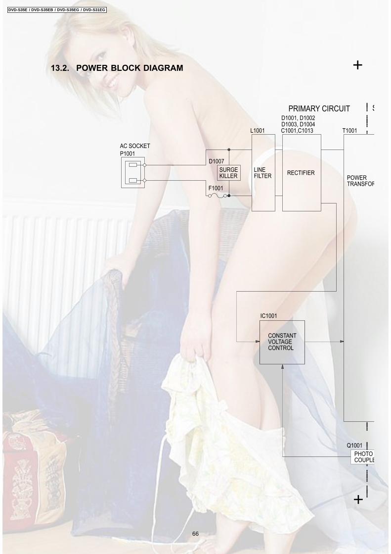
13.2. POWER BLOCK DIAGRAM
SPRIMARY CIRCUIT
Q1001
IC1001
CONTROLVOLTAGECONSTANT
TRANSFORPOWER
T1001C1001,C1013
D1001, D1002D1003, D1004
RECTIFIER
L1001
FILTERLINE
D1007
KILLERSURGE
F1001
AC SOCKET
P1001
COUPLEPHOTO
+
+
DVD-S35E / DVD-S35EB / DVD-S35EG / DVD-S31EG
66
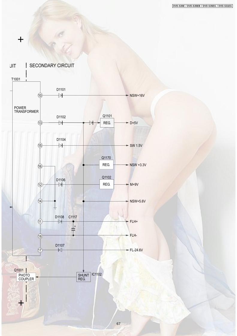
+
SECONDARY CIRCUITUIT
Q1001
NSW+5.6V
FLH-
FLH+
M+9V
NSW +3.3V
FL-24.6V
SW 1.5V
D+5V
NSW+16V
REG.SHUNT IC1102
15
16
Q1101
Q1102
Q1170
11
18
17
12
14
REG.13
10
TRANSFORMERPOWER
T1001
D1101
D1102
D1104
D1107
D1108
D1106
C1117
REG.
REG.
COUPLERPHOTO
+
+
DVD-S35E / DVD-S35EB / DVD-S35EG / DVD-S31EG
67
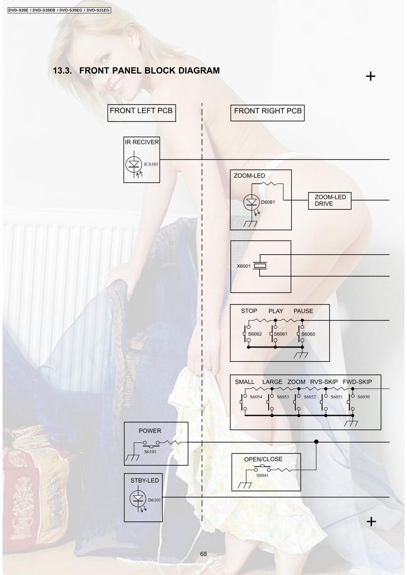
13.3. FRONT PANEL BLOCK DIAGRAM
S6052 S6051 S6050
S6062 S6061 S6060
04S6 1
S6101
D6101
IC6101
FRONT LEFT PCB
SMALL ZOOM RVS-SKIP FWD-SKIP
STOP PLAY PAUSE
D6081
ZOOM-LED
STBY-LED
POWER
IR RECIVER
FRONT RIGHT PCB
S6053S6054
LARGE
NOPE /CLOSE
X6001
ZOOM-LEDDRIVE
+
+
DVD-S35E / DVD-S35EB / DVD-S35EG / DVD-S31EG
68
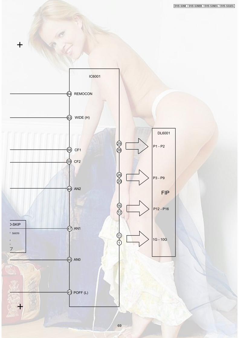
S6050
D-SKIP
63
43
46
64
47
48
58
59
IC6001
FIP
DL6001
1
20
12
11
26
28
29
16
P1 - P2
REMOCON
WIDE (H)
CF1
CF2
AN2
AN1
AN0
POFF (L)
P3 - P9
P12 - P16
1G - 10G
+
+
DVD-S35E / DVD-S35EB / DVD-S35EG / DVD-S31EG
69

13.4. SERVO BLOCK DIAGRAM (Decoder PCB)
BIAS1
BIA
IC6001-41,42PINFROM LDIN
24
OPOUT6
AD0
VIN3
VIN2
VIN1
TRIN
SPDRV
FODRV
TRDRV
TRSDRV
71
70
2
26
23
3
(MOTOR DRIVE)IC2501
RFINN
RFINP
LASER DIODE Q5121, Q5122
LD DRIVE
VIN10
VIN9
VIN4
VIN3
VIN2
VIN1
VIN8
VIN7
VIN6
VIN5
OPTICAL PICK UP UNIT
PHOTO DETECTOR
B3B4
B2B1
A3
A2
A4
A1
LASER DIODE
AMPHEAD
Q5131, Q5132
LD DRIVE
122
(DV1)IC3001
123
124
125
126
127
128
129
130
131
133
132
135
134
120
121
148
152
150
F
G
E
D
C
B
A
54321 6
DVD
CD
Tray DRV
+
DVD-S35E / DVD-S35EB / DVD-S35EG / DVD-S31EG
70
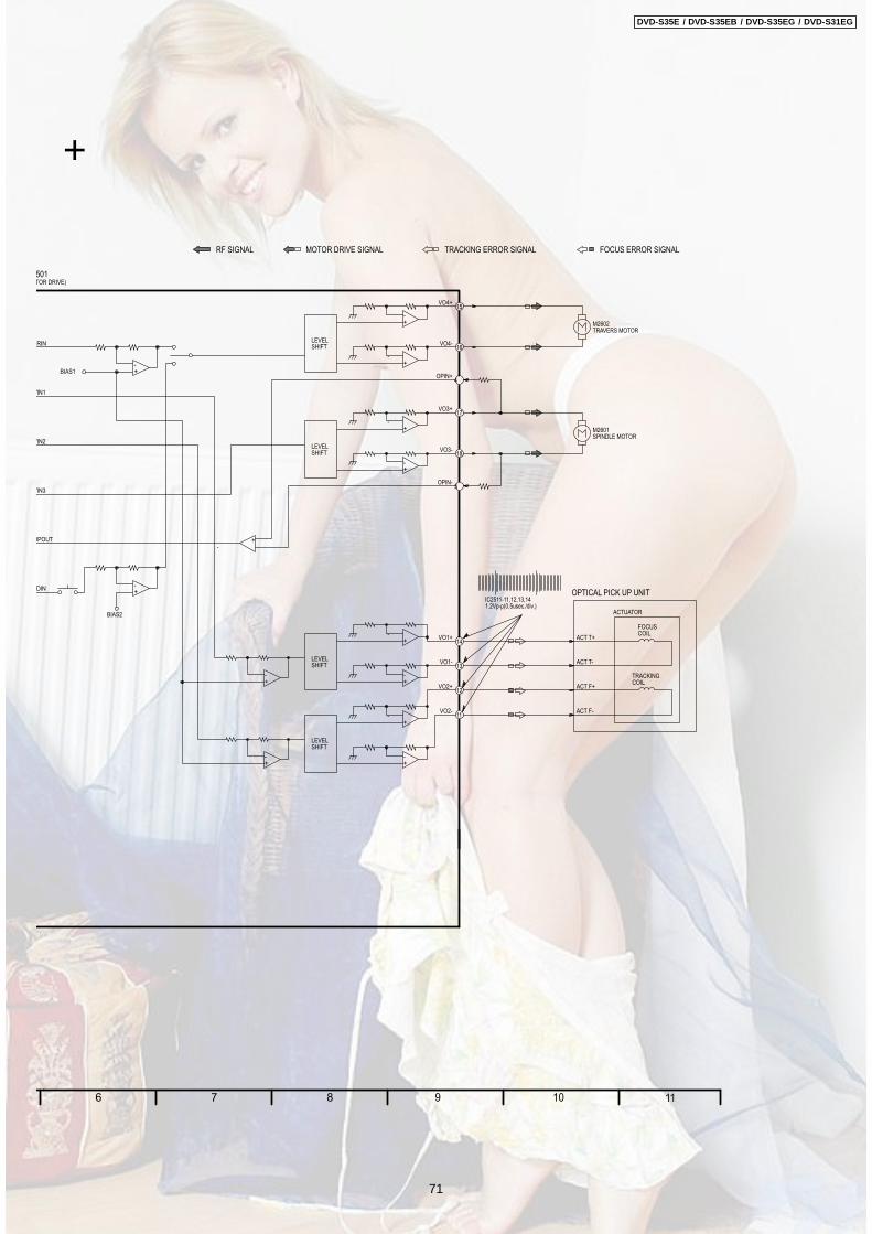
BIAS1
BIAS2
-+
SHIFT
-
LEVEL
+
+-
+-
SHIFT
-
LEVEL
+
-+
+-
SHIFT
-
LEVEL
+
+-
+-
SHIFTLEVEL
-+
+-
+-
OPIN-5
OPIN+4
SPINDLE MOTORM2601
TRAVERS MOTORM2602
DIN
OPOUT
1.2Vp-p(0.5usec./div.)IC2511-11,12,13,14
RF SIGNAL MOTOR DRIVE SIGNAL TRACKING ERROR SIGNAL FOCUS ERROR SIGNAL
VIN3
VIN2
VIN1
RIN
VO2-
VO2+
VO1-
VO1+
VO3-
VO3+
VO4-
VO4+
11
12
13
14
18
17
16
15
TOR DRIVE)501
ACT F-
ACT F+
ACT T-
ACT T+
OPTICAL PICK UP UNIT
ACTUATOR
COILTRACKING
COILFOCUS
9 10876 11
+
DVD-S35E / DVD-S35EB / DVD-S35EG / DVD-S31EG
71

14 SCHEMATIC DIAGRAM14.1. INTERCONNECTION SCHEMATIC DIAGRAM
F
G
E
D
C
B
A
54321 6
1 TRAY2 D GN
5
DT
R-
S
P-M
OO
SP - O OD M T R-
FG3
T
R6
S
PD
-MO
O+
SPD- O OM T R+
FG2
7 T
RV
-T
R-
MO
O
V- O OTR M T R-
FG2
8
RV
-T
R
TM
OO
+
V- O O +TR M T R
FG1
4
N(F
G
D
G2
)
2)GND (FG
2
F
G3
FG3
R
-3
T
VS
W
V- WTR S
5
1
6
2
7
3
8
4
4
3
2
1
JK3801
Terminal PCB Unit
FG PCB Unit
Mechanism Unit
FP5101
FP2501
T(+)
F(+)
F(-)
T(-)
3.3V HFM
GND
LD(+)(DVD)
GND
GND
RF P
RF N
F1(DVD)
F2(DVD)
GAIN H/L
P IN(DVD)
V REF2.2(DVD)
TA(DVD)
TD(DVD)
TC(DVD)
TB(DVD)
VCC 5V
FE1
GND
LD(+)(CD)
T1(CD)
V REF2.2(CD)
FE2(CD)
T2(CD)
P IN(CD)
GND
30
29
28
27
26
25
24
23
22
21
20
19
18
17
16
15
14
13
12
11
9
10
8
7
6
5
4
3
2
1
SWITCHOPENTRAY
Decoder PCB Unit
Front PC
F
Optical Pickup Unit
Front PCB Unit PP6101
P1
FC6101
FP2601
FP2602
1
FG
1
FG1
1
5
4
2
3
1
5
4
2
3
STBLEDSTBLEDNSW+3.3VNSW+3.3VPOWER-SWPOWER-SWREMOCONREMOCONDGNDDGND
+
DVD-S35E / DVD-S35EB / DVD-S35EG / DVD-S31EG
72
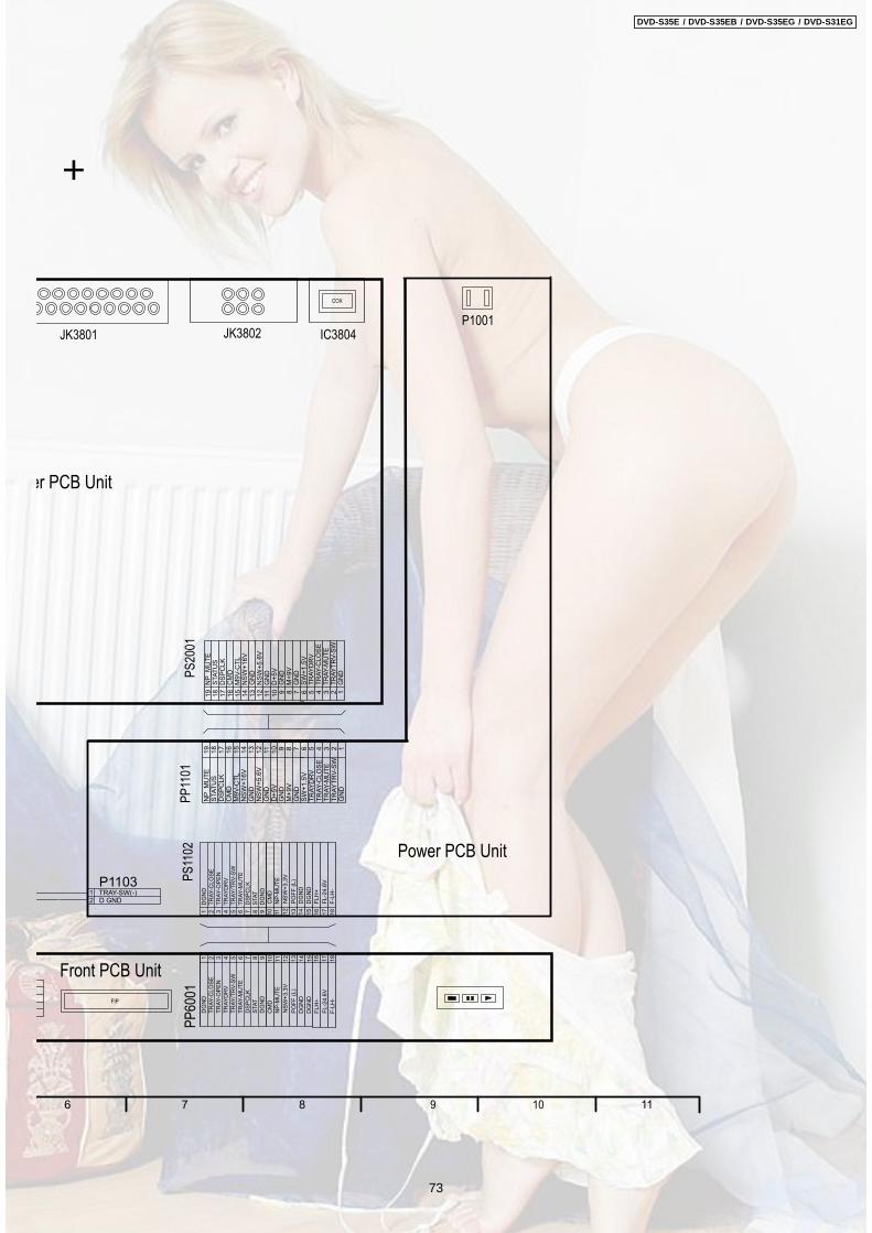
9 10876 11
1 TRAY-SW(-)2 D GND
JK3802 IC3804P1001
COX
JK3801
er PCB Unit
Power PCB Unit
Front PCB Unit
PS
2001
PP
1101
FIP
9
DG
ND
DG
ND
7
DS
PC
LK
DS
PC
LK
8
STA
TS
TA
T
9 10
12
11
13
14
15
16
17
187 8
PS
1102
PP
6001
11
D
GN
DD
GN
D
6
TR
AY
-MU
TE
TR
AY
-MU
TE
5
TR
AY
/TR
V-S
WT
RA
Y/T
RV
-SW
4
TR
AY
DR
VT
RA
YD
RV
2
TR
AY
-CL
OS
ET
RA
Y-C
LO
SE
3
TR
AY
-OP
EN
TR
AY
-OP
EN
6542 3
P1103
10
C
MD
CM
D
11
N
P-M
UT
EN
P-M
UT
E
12
N
SW
+3
.3V
NS
W+
3.3
V
13
P
OF
F (
L)
PO
FF
(L
)
14
D
GN
DD
GN
D
15
D
GN
DD
GN
D
16
F
LH
+F
LH
+
17
F
L-2
4.6
VF
L-2
4.6
V
18
F
-LH
-F
-LH
-
66
55
44
33
22
11
77
88
99
10
10
11
11
12
12
13
13
14
14
15
15
16
16
17
17
18
18
19
19
SW
+1
.5V
SW
+1
.5V
GN
DG
ND
NS
W+
16
VN
SW
+1
6V
GN
DG
ND
D+
5V
D+
5V
GN
DG
ND
M+
9V
M+
9V
GN
DG
ND
CM
DC
MD
DS
PC
LK
DS
PC
LK
STA
TU
SS
TA
TU
SN
P_M
UT
EN
P_M
UT
E
NS
W+
5.6
VN
SW
+5
.6V
TR
AY
-MU
TE
TR
AY
-MU
TE
TR
AY
TR
V-S
WT
RA
YT
RV
-SW
TR
AY
DR
VT
RA
YD
RV
TR
AY
-CLO
SE
TR
AY
-CLO
SE
M9V
-CT
LM
9V
-CT
L
GN
DG
ND
+
DVD-S35E / DVD-S35EB / DVD-S35EG / DVD-S31EG
73
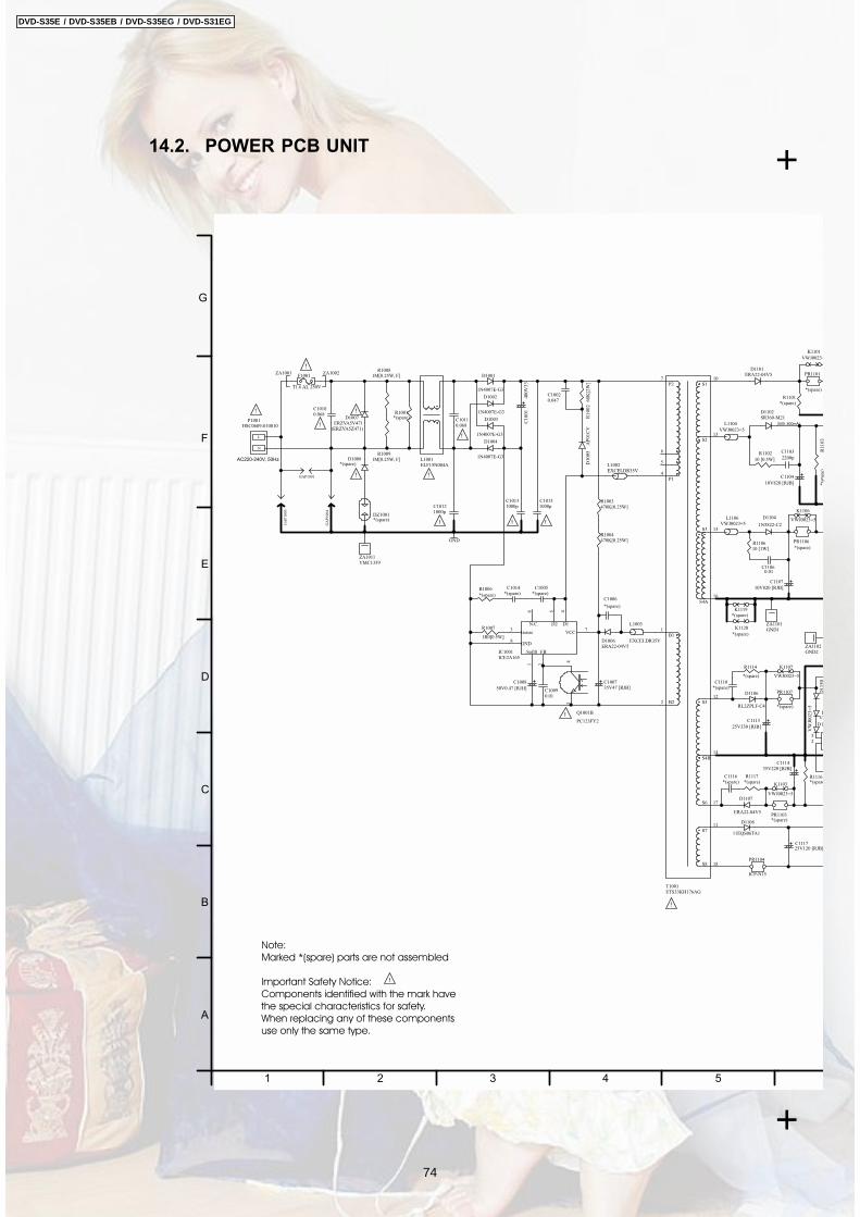
14.2. POWER PCB UNIT
GND
R1001*(spare)
L1001ELF15N004A
D11
50
DVW
D1
VW
J00
23
=5
1 2
3
456
7
8
SoftS FB
VCC
D1D2N.C.
Isense
GND
IC1001ICE2A165
D1006ERA22-04V5
R1102
10 [0.5W]
C1103
2200p
R110610 [1W]
D1107
ERA22-04V5
R1116*(spare
C111725V120 [RJB]
R1117*(spare)
D1008*(spare)
DZ1001*(spare)
R1101*(spare)
!
C1014*(spare)
!
C1005*(spare)
!
AC220-240V, 50Hz
!
!
!
GA
P1
00
5
!GA
P1
00
4
GAP1001
!
!
!
!
P2
P1
B1
B2
!
S1
S2
S3
S4A
S5
S4B
S6
S7
S8
R1114
*(spare)
(500..800mA)
L
N
P1001HSC0609-010010
R11
03
*(s
par
e)
R1004470K[0.25W]
R1003470K[0.25W]
R1
00
26
8K
[2W
]R1006
*(spare)
D1
00
5A
P0
1C
V
43
Q1001B
PC123FY2
C1
00
14
00
V3
3
C1006
*(spare)
C10090.01
C10100.068
C10110.068
C10121000p
C10131000p
C11060.01
C1110*(spare)
C1116*(spare)
D1007ERZVA5V471
D1104
1N5822-C2
52
L1002EXCELDR35V
C10020.047
F1001
T1.6 AL 250V
ZA1011VMC1359
ZA1102GND2
ZA1101GND1
(ERZVA5Z471)
R1007
1R0[0.5W]
D1101ERA22-04V5D1001
1N4007E-G3
D1002
1N4007E-G3
D1004
1N4007E-G3
D1003
1N4007E-G3
C100735V47 [RJB]
L1003
EXCELDR35V
2
1
4
7
5
6
10
13
15
16
12
14
17
11
18
T1001ETS33KH176AG
D1102SR360-M21
C1113
25V330 [RJB]
D1108
11EQS06TA1
D1106
RL2ZPLF-C4
ZA1001 ZA1002
L1104
VWJ0023=5
L1106VWJ0023=5
C1008
50V0.47 [RJH]
C111435V220 [RJB]
C1104
10V820 [RJB]
C1107
10V820 [RJB]
R10081M[0.25W, F]
R10091M[0.25W, F]
C10151000p
!
PR1101
*(spare)
PR1106
*(spare)
PR1107
*(spare)
PR1103*(spare)
PR1104
ICP-N15
K1101
VWJ0023=
K1106
VWJ0023=5
K1107
VWJ0023=5
K1103
VWJ0023=5
K1119*(spare)
K1120
*(spare)
Note: Marked *(spare) parts are not assembled
Important Safety Notice:Components identified with the mark have the special characteristics for safety.When replacing any of these components use only the same type.
F
G
E
D
C
B
A
54321
+
+
DVD-S35E / DVD-S35EB / DVD-S35EG / DVD-S31EG
74

D11
50
VW
J00
23
=5
D1151VWJ0023=5
D1152
VW
J00
23
=5
M9V-CTLM9V-CTL
GND
C110125V120 [RJB]
NP-MUTE
TRAY-CLOSE
L110210u
TRAYDRV
TRAYTRV-SW
TRAY-MUTE
NP-MUTE
NP-MUTE
TRAY-MUTE
R1102
10 [0.5W]
TRAY-MUTE
C1103
2200p
TRAYTRV-SW
TRAYTRV-SWTRAYDRV
TRAYDRVTRAY-CLOSE
TRAY-CLOSE
R110610 [1W]
L1103
10u
DSPCLKSTAT
CMD
N_SW+16V
CMD
NSW5.6V
DSPCLKSTAT
D+5V
GND
SW+1.5V
DGNDTRAY-OPEN
DGND
DGND
POFF(L)
07
2-04V5
TRAY-CLOSE
TRAY-OPEN
FL-24.6V
NSW+3.3V
DGND
FLH-
FLH+
R1116*(spare)
CMD
DSPCLK
STAT
NP-MUTE
TRAY-MUTE
TRAY/TRV-SW
TRAYDRV
654321
789101112131415161718
PS1102
TMC-D18X-A1
M+9V
C111725V120 [RJB]
L1105VWJ0023=5
R1117spare)
R1101*(spare)
GND
GND
GND
GND
STATUS
DSPCLK
CMD
!
12
Q1001APC123FY2
1114
spare)
DGND
654321
78910111213141516171819
PP1101
TWG-P19P-A1
TW1101
TW1104
TW1103TW1125
TW1133
TW1116 TW1109 TW1105 TW1106
(2.5V/500..700mA)
(500..800mA)
D111
0*(s
par
e)
R11
03
*(s
par
e)
R11
05
*(s
par
e)
R11091K[0.25W]
R111
22
K[0
.25
W]
R11
08
3K
3[0
.25
W]
R11
22
11
,8K
[0.2
5W
;1%
]
R11131K2[0.25W;1%]
R1107*(spare)
L1101
220uH
C11060.01
C1115
*(spare)
D1104
1N5822-C2
D1170
MAZ40390HF
IN5
SW2
1
SENS4
OUT3
IC1150SI-3090FLF1113
54321
P1104
*B5B-PH-K-S
CMD
DSPCLK
STATDGND
CMD
STATUS
DSPCLK
NSW+3.3V
(to Front R)
(to Mecha)
(to AV Decoder PCB)
ZA1102GND2
ZA1101GND1
Q11702SD1992ARA
D1101RA22-04V5
12
P1103
B2B-PH-K
D1160
1N4007E-G3
R1110100[0.25W]
R11
70
22
0[0
.25
W]
Q11022SB14170JA
D1102SR360-M21
R1150
330[0.25W]
R1115
100K[0.25W]
R1192
68[0.25W]
Q1171 2SD1996
Q11722SD1996
R1174220[0.25W]
R1173
220[0.25W] R11751500[0.25W]
R11761K[0.25W]
R1153
2K2[0.25W]
R1152
150[0.25W]
D115311ES1-TA1B2
C1113
[RJB]
C11180.1 [ECQV]
C11720.1 [ECQV]
108
06TA1
C11
70
0.1
[E
CQ
V]
D11
03
11
EF
S2
-TA
1B
2
D1106
ZPLF-C4
Q11732SD1992ARA
QR1101
UNR421300A
C11626V100 [RJB]
C11716V100 [RJB]
R1171 1R2 [0.5W]
R1172 1R2 [0.5W]
C11
51
16
V4
7 [
RJB
]
R1177220[0.25W]
C1108
16V47 [RJB]
C111435V220 [RJB]
C110225V47 [RJB]
C1104
10V820 [RJB]
C11
05
25
V4
7 [
RJB
]
C1107
10V820 [RJB]
C1111
25
V2
20 [
RJB
]
C111
91
6V
47
[R
JB]
IC11
02
MM
14
31
AT
T
Q11012SD2177-R(TA)
R11
51
39
0[0
.5W
]
PR1105
ICP-N20
R11
04
47
0[0
.25
W]
PR1101
*(spare)
PR1102
*(spare)
PR1106
*(spare)
PR1107
*(spare)
PR1103*(spare)
PR1104
ICP-N15
K1101
VWJ0023=5
K1102
VWJ0023=5
K1106
VWJ0023=5
K1107
VWJ0023=5
K1103
VWJ0023=5
R1111
43
20 [
0.2
5W
;1%
]
K111
4*(s
par
e)
K111
5*(s
par
e)
K111
6*(s
par
e)
)
C1109
0.1
IC1171MM1530ATT
9876 1110
+
+
DVD-S35E / DVD-S35EB / DVD-S35EG / DVD-S31EG
75
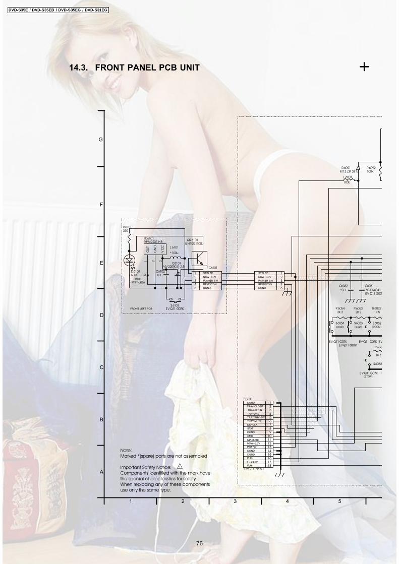
14.3. FRONT PANEL PCB UNIT
S6052
EV Q11 G07K EV
S6062
EV Q11 G07K E
R60521K 5
R606
1K 5
R60532K 2
R60543K 3
R6092100K
S6041EV Q11 G07K
TRAYDRV
TRAY/TRV-SW
TRAY-MUTE
C6031
*0.1
C6032
*0.1
NP-MUTE
STAT
DSPCLK
CMD
STBLEDSTBLED
NSW+3.3VNSW+3.3V
POWER-SWPOWER-SW
REMOCON REMOCON
DGND DGND
OU
T1
GN
D2
VC
C3
I C6101RPM7237-H8
C61020.1
S6101EV Q11 G07K
D6101L NJ201L PQJA
FRONT LEFT PCB
FLH+
FLH-
DGND
NSW+3.3V
FL-24.6V
L 6001
100U
TRAY-OPEN
TRAY-CLOSE
POFF(L)
DGND
DGND
(small) (ZOOM)
(STOP)
(red)
(STBY-LED)
DGND
S6053
EV Q11 G07K
S6054
EV Q11 G07K
(large)
R6101330
654321
789
101112131415161718
PP6001
T MC-D18P-A1
C6101*4V 220[K S]-2.5
L 6101
*100u
54321
54321
FC6101
D6091MT Z J3R3B T A
QR6101U NR221100L
!
Note: Marked *(spare) parts are not assembled
Important Safety Notice:
Components identified with the mark have the special characteristics for safety.When replacing any of these components use only the same type.
F
G
E
D
C
B
A
54321
+
DVD-S35E / DVD-S35EB / DVD-S35EG / DVD-S31EG
76

R6025
10K
R602110K
R6023
10K
C6002
0.1
C6012 0.1
C60110.1
R6003*47K
R600247K
C6021*0.1
C6003
0.1
S6052
EV Q11 G07K
S6051
EV Q11 G07K
S6050
EV Q11 G07K
S6062
EV Q11 G07K
S6061
EV Q11 G07K
S6060EV Q11 G07K
R6061
1K 2
R60511K 2
R60521K 5
R6062
1K 5
R60532K 2
R6092100K
S6041EV Q11 G07K
R60411K 2
R6040
10K
R6060
10K
R6050
10KC6060
0.01
C60500.01
C60400.01
C6031
*0.1
2
C60040.1
C609150V 0.01
R6018
*47K
R 6019*47K
001
0U
(ZOOM) (RVS-SKIP) (FWD-SKIP)
(STOP) (PLAY)
(PAUSE)
QR6081DT A123JK
D6081L NJ301MPU JAD
(ZOOM-LED)
(green)
S6053
1 G07K
(large)
PITCH=2.5mm
PITCH=2.5mm
R6081330
C600550V 10[K S]-2.5
C60014V 220[K S]-2.5
(OPEN/CLOSE)
R609110K
Q60912SD1328-T X
C6006
50V 0.01
R6017 *47KR6015 *47KR6014 *47K
R6016 *47K
R6013 *47KR6012 *47KR6011 *47KR6010 *47K
XO
GN
DXI
321
X 6001CST S0800MG03-T 2
091J3R3B T A
F-
1
NP
5
10G
6
P2
7
P3
8
NP
9
NP
10
P4
11
NP
12
9G
13
P5
14
NP
15
NP
16
P6
17
NP
18
NP
19
P7
20
NP
21
8G
22
P8
23
NP
24
NP
25
P9
26
NP
27
P10
29
7G
28
NP
30
6G
31
P11
32
NP
33
5G
34
F-
2
NP
3
P1
4
P12
35
NP
36
4G
37
P13
38
NP
39
3G
40
P14
41
NP
42
2G
43
NP
44
1G
45
NP
46
P15
47
P16
48
NP
49
F+
50
F+
51
DL 600110-B T -251GNK
R600110K
FL -DGT 01
FL -DGT 12
FL -DGT 23
FL -DGT 34
FL -DGT 45
FL -DGT 56
FL -DGT 67
FL -DGT 78
V DD39
FL -DGT 810
FL -DGT 911
FL -SEG012
FL -SEG113
FL -SEG214
FL -SEG315
FL -SEG416
17
18
19
FL
-SE
G7
20
FL
-SE
G8
21
FL
-SE
G9
22
FL
-SE
G10
23
FL
-SE
G11
24
FL
-SE
G12
25
FL
-SE
G13
26
VD
D4
27
FL
-SE
G14
28
FL
-SE
G15
29
RG
B(H
)30
YC
(H)
31
CO
MP(L
)32
333435
CMD36
ST AT37
DSPCL K38
T RAY -MU T E39
T RAY /DRV -SW40
P1541
P1642
POFF(L )43
V SS244
V DD245464748
AN
349
AN
450
AN
551
ZO
OM
LE
D52
NP-M
UT
E53
RE
SE
T54
TR
AY
OPE
N55
TR
AY
CL
OSE
56
VSS1
57
CF1
58
CF2
59
VD
D1
60
SC
AR
T(L
)61
62
63
64
17 FL -SEG518 V P (-30,6V )
19 FL -SEG633 OFFMU T E
34 NFL OFF35 PF7
46 AN047 AN1
48 AN262 W IDE63 W IDE(H)64 REMOCON
I C6001
L C876332A-51A1-E
(MASK)
or HNV-10SS26T
R6072 47KR6071 30K
VSS
4
VD
D2
NC
3
OU
T1
I C6002PST 3327U R
R6022
*S1
R6024
*S2
R6026
*S3
1
876 11109
+
DVD-S35E / DVD-S35EB / DVD-S35EG / DVD-S31EG
77
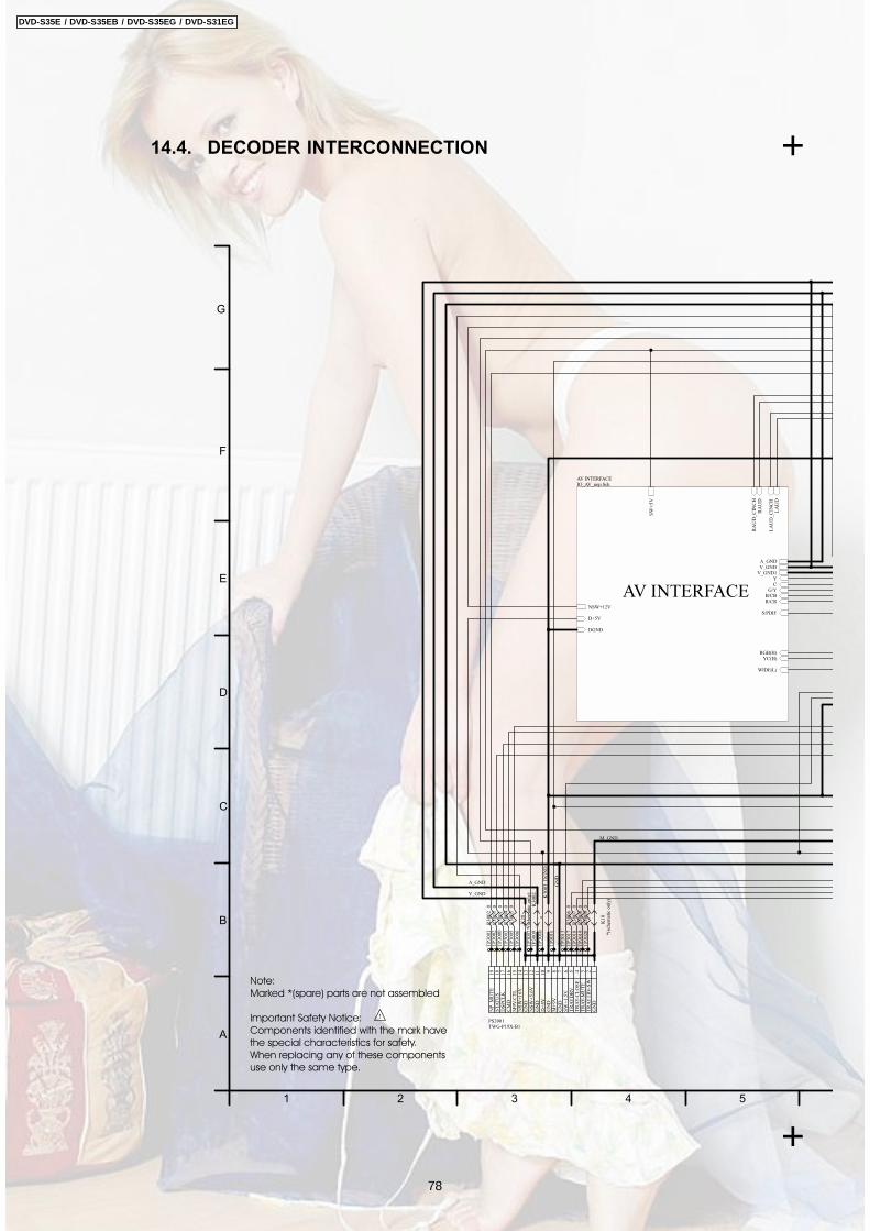
14.4. DECODER INTERCONNECTION
SW
+5
V
A_GNDV_GND
YC
G/YB/CBR/CR
LA
UD
LA
UD
_C
INC
H
RA
UD
RA
UD
_C
INC
H
NSW+12V
RGB(H)YC(H)
WIDE(L)
D+5V
DGND
S/PDIF
V_GND1
AV INTERFACEIO_AV_nop.Sch
AV INTERFACE
TP
30
02
TP
3003
TP
3001
TP
3005
TP
3007
TP
3009
TP
3011
TP
3013
TP
3017
TP
3018
TP
3019
TP
3020
TP
30
00
TP
3006
R3
00
90
R3
00
10
R3
00
20
R3
00
30
R3
00
40
R3
00
50
R3
00
60
R3
00
70
R3
00
80
6 5 4 3 2 178910
11
12
13
14
15
16
17
18
19
PS2001TWG-P19X-B1
SW
+1
.5V
GN
D
NS
W+
16
V
GN
DD
+5
V
GN
DM
+9
V
GN
D
CM
DD
SP
CL
KS
TA
TU
SN
P_M
UT
E
NS
W+
5.6
V
TR
AY
-MU
TE
TR
AY
TR
V-S
W
TR
AY
DR
VT
RA
Y-C
LO
SE
M9V
-CT
L
GN
D
TP
30
10
K3
00
3
M_GND
GN
DDG
ND
A_GND
V_GND
K3
00
2
*
K20
*(s
chem
atic
only
)
K10
*(s
chem
atic
only
)
!
Note: Marked *(spare) parts are not assembled
Important Safety Notice:Components identified with the mark have the special characteristics for safety.When replacing any of these components use only the same type.
F
G
E
D
C
B
A
54321
+
+
DVD-S35E / DVD-S35EB / DVD-S35EG / DVD-S31EG
78

EXADT[0..15]EXADR[16..20]
NEXWE
TRCDATA0TRCDATA1
NEXCENEXOE
TRCCLK
TRCDATA2TRCDATA3
TRCST
DR
V3
DR
V4
DR
V7
DR
V8
PNRSTSCLOCK
EXTRG0SDATA
D+3.3V
TR
V-S
WS
PD
RV
TR
DR
VF
OD
RV
TR
SD
RV
AD
0
AD
2V
HA
LF
LP
C2
VIN
6V
IN9
VIN
10
VIN
5V
IN4
VIN
3V
IN2
VIN
1V
RE
FH
LP
C1
VIN
8V
IN7
RF
INN
RF
INP
LP
CO
2L
PC
O1
GND
EX
TC
LK
1
S/PDIF
V_GND
YCG/YB/CBR/CR
SR
CK
LR
CK
DM
IXO
UT
DGNDD+1.5V
P[0
..1
5]
D+5V
ST
AT
US
DS
PC
LK
CM
D
RGB(H)YC(H)
WIDE(L)
M9V
-CT
L
FG
FG
EN
B
V_GND1
DV1DV1.sch
EXADT[0..15]EXADR[16..20]NEXWE
TRCDATA0TRCDATA1
NEXCENEXOE
P[0
..1
5]
TRCCLK
TRCDATA2TRCDATA3TRCST
PNRSTSCLOCK
EXTRG0SDATA
D+3.3V
DG
ND
FLASH MEMORYFMEM.sch
AV DECODERFLASH MEMORY
TR
V-S
WS
PD
RV
TR
DR
VF
OD
RV
TR
SD
RV
AD
0
AD
2V
HA
LF
LP
C2
VIN
10
VIN
6V
IN9
VIN
5V
IN4
A+5V
VIN
3V
IN2
LP
C1
VR
EF
HV
IN1
VIN
8V
IN7
RF
INN
RF
INP
LP
CO
2L
PC
O1
D+5V
GND
D+3.3V
HF
MO
NM
UT
E3
GA
IN H
/LM
UT
E1
2
M+9V
M_GND
TRAY/TRVTRAY-MUTE
TRAYDRVTRV-SW
DGND FG
FG
EN
B
DRIVE CONNECTIONPRE.sch
DRIVE CONNECTION
A_GND
D+3.3V
DGND
DM
IXO
UT
EX
TC
LK
1
LAUD_CINCHLAUD L
RC
K
NSW+12V
NSW+16V
RAUD_CINCHRAUD
P[0
..1
5]
SR
CK
SW+5V
NSW+5.6V
GND
V_GND
M+9V
NP_MUTE
AUDIO DACADAC.sch
AUDIO DAC
A_GNDV_GND
YC
G/YB/CBR/CR
LA
UD
LA
UD
_C
INC
H
RA
UD
RGB(H)YC(H)
WIDE(L)
S/PDIF
V_GND1
876 119 10
+
+
DVD-S35E / DVD-S35EB / DVD-S35EG / DVD-S31EG
79
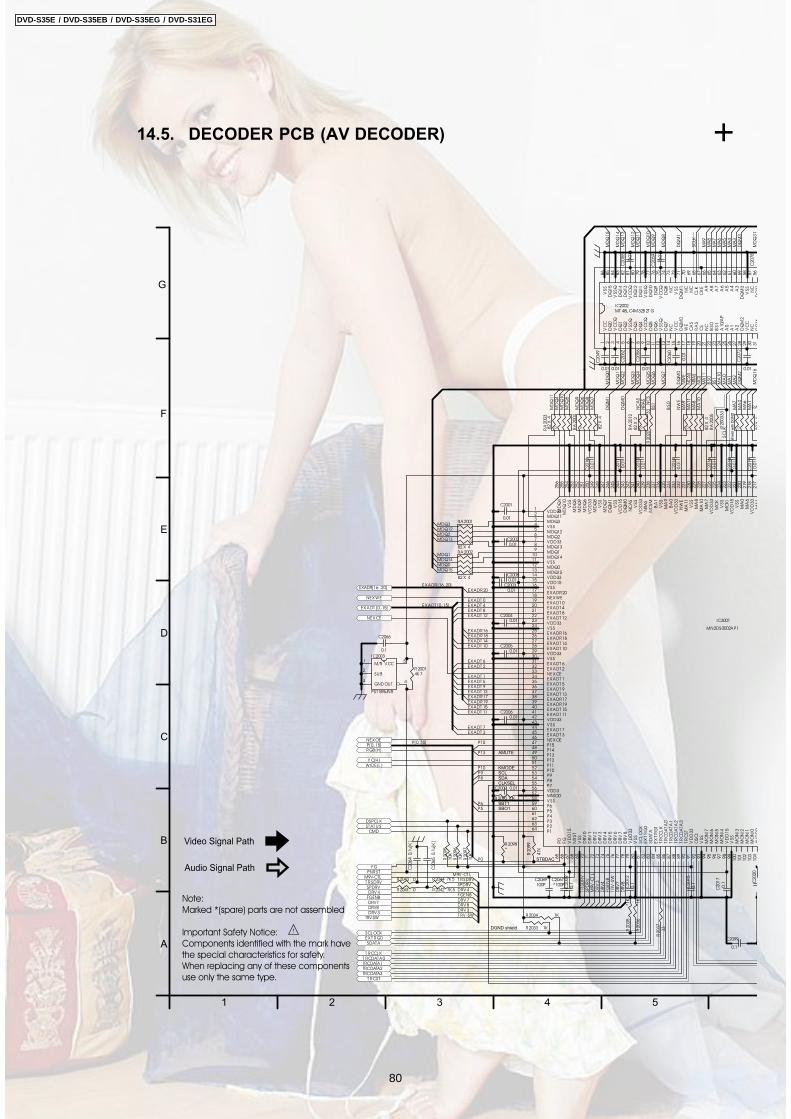
14.5. DECODER PCB (AV DECODER)
C2019
0.0
1
C2018
0.0
1
C2016
0.0
1
C2014
0.0
1
C2013
0.0
1
C2011
0.0
1
C2010
0.0
1
C2001
0.01
C20020.01
C20080.01
C20040.01
C20050.01
C20060.01
C2007 0.01
C20030.01
C2020
01
RA
2005
82 X
4
RA
82
X4
RA
2003
82 X
4
RA
2004
82 X
4
MDQ0
MDQ1
MDQ2
MDQ3
MD
Q4
MD
Q5
MD
Q6
MD
Q7
MD
Q8
MD
Q9
MD
Q10
MD
Q1
1
MDQ12
MDQ13
MDQ14
MDQ15
MA
0
MA
1M
A6
MA
7
MA
8
MA
9
MA
10
MA
11
C2078
C2059
0.0
1
C2055
0.0
1
C2049
0.01
C2052
0.01
C2058
0.01
C2060
0.0
1
C2072
0.01
MD
Q0
MD
Q1
MD
Q2
MD
Q3
MD
Q4
MD
Q5
MD
Q6
MD
Q7
MD
Q8
MD
Q9
MD
Q10
MD
Q1
1M
DQ
12
MD
Q1
3M
DQ
14
MD
Q1
5
MD
Q1
6M
DQ
31
MA
0M
A1
MA
2M
A3
MA
4M
A5
MA
6M
A7
MA
8M
A9
MA
10
MA
11
DQ
M0
DQ
M1
DQ
M2
DQ
M3
BS
0BS1
NW
E
NC
SN
RA
SN
CA
S
NC
AS
NRA
SN
CS
NW
E
DQ
M0
DQ
M1
BS
0
BS1
EX ADR16
EX ADR17
EX ADR18
EX ADR19
EX ADR20EX ADR[16..20]
EXADR[16..20]
EX ADT 0
EX ADT 1
EX ADT 2
EX ADT 3
EX ADT 4
EX ADT 5
EX ADT 6
EX ADT 7
EX ADT 8
EX ADT 9
EX ADT 10
EX ADT 11
EX ADT 12
EX ADT 13
EX ADT 14
EX ADT 15
EX ADT [0..15]EX ADT [0..15]
NEX WE
NEX CE
NEX OE
P8P9P10
P13
P[0..15]P[0..15]
KMODESCLSDA
P0
SBT1SBO1
PNRST
DRV 4
DRV7DRV8
T RSDRVSPDRV
DRV 3
TR
SD
RV
T RSDRVSPDRV
SPD
RV
DR
V3
DRV4
DRV7
DRV8
DRV 3
DRV 4
DRV 7DRV 8
TR
V-S
W
T RV -SWTRV-SW
R2033 1K R2036
*1K
R2035
*1K
R2034 1K
SCL OCKEX T RG0SDAT A
T RCCL KT RCDAT A0TRCDATA1TRCDATA2TRCDATA3
T RCST
R2037
33DGND shield
C2099
0.1
P5P6
CLKSEL
SC
LK
SCLK
AMUTE
STBDAC
DQ
713
NC
14
VC
C15
DQ
M0
16
WE
17
CA
S18
RA
S19
CS
20
NC
21
BS
022
BS
123
A10/A
P24
A0
25
A1
26
A2
27
DQ
M2
28
VC
C29
NC
30
DQ
16
31
VC
C1
DQ
02
VC
CQ
3
DQ
14
DQ
25
VS
SQ
6
DQ
37
DQ
48
VC
CQ
9
DQ
510
DQ
611
VS
SQ
12
DQ
31
56
NC
57
VS
S58
DQ
M3
59
A3
60
A4
61
A5
62
A6
63
A7
64
A8
65
A9
66
CK
E67
CL
K68
NC
69
NC
70
DQ
M1
71
VS
S72
NC
73
DQ
874
DQ
976
DQ
10
77
VSSQ
78
DQ
1179
DQ
12
80
VC
CQ
81
DQ
13
82
DQ
14
83
VSSQ
84
DQ
15
85
VS
S86
VC
CQ
75
IC2002MT 48L C4M32B 2T G
V CC5
GND3
OU T4
M/R1
SU B2
IC2003
PST 596JNR
DSPCL KST AT U S
CMD
R2095
10K
R2096
10K
R2097
10K
P15
R2044 7K 5
R2042 7K 5
R2043 0
R2041 0
R2090 10K
RGB (H)
Y C(H)WIDE(L )
M9V
-CT
LM9V -CT LM9V-CTL
C2064
0.1
u[K
]
C2065
0.1
u[K
]
C2089100P
C2017
0.1
C2015
0.1
C2012
0.1
C2009
0.1
R20014K 7
C2066
0.1
RA
2012
82 X
2
R200333
R2099
47K
R2098*
FG
EN
B
FGENBFGENB
FG
V DD331
MDQ112
MDQ33
V SS4
MDQ125
MDQ26
V DD337
MDQ138
MDQ19
MDQ1410
V SS11
MDQ012
MDQ1513
V DD3314
V DD1515
V SS16
EX ADR2017
NEX WE18
EX ADT 019
EX ADT 420
EX ADT 821
EX ADT 1222
V DD3323
V SS24
EX ADR1625
EX ADR1826
EX ADT 1427
EX ADT 1028
V DD3329
V SS30
EX ADT 631
EX ADT 232
NEX CE33
EX ADT 134
EX ADT 535
EX ADT 936
EX ADT 1337
EX ADR1738
EX ADR1939
EX ADT 1540
EX ADT 1141
V DD3342
V SS43
EX ADT 744
EX ADT 345
NEX OE46
P1547
P1448
P1349
P1250
P1151
P1052
P953
P854
P755
V DD356
MMOD57
V SS58
P659
P560
P461
P362
P263
P164
P0
65
FG
66
VD
D15
67
NR
ST
68
VSS
69
DR
V0
70
DR
V1
71
DR
V2
72
DR
V3
73
DR
V4
74
DR
V5
75
DR
V6
76
DR
V7
77
DR
V8
78
VD
D33
79
VSS
80
SC
LO
CK
81
EX
TR
G0
82
SD
ATA
83
EX
TR
G1
84
TR
CC
LK
85
TR
CD
ATA
086
TR
CD
ATA
187
TR
CD
ATA
288
TR
CD
ATA
389
TR
CST
90
VD
D33
91
OSC
I92
VSS
93
MO
NI7
94
MO
NI6
95
MO
NI5
96
MO
NI4
97
VD
D15
98
VSS
99
MO
NI3
100
MO
NI2
101
MO
NI1
102
MO
NI0
103
AV
DD
D104
MA
1217
VD
D33
218
MA
6219
MA
0220
VS
S221
VD
D15
222
MC
KI
223
VS
S224
MC
K225
VD
D33
226
MA
7227
MA
10
228
MA
8229
VS
S230
MA
11231
NW
E232
VD
D33
233
BA
0234
MA
9235
VS
S236
BA
1237
NC
SM
238
NRA
S239
VD
D33
240
VS
S241
NC
AS
242
DQ
M0
243
VD
D15
244
VS
S245
DQ
M1
246
MD
Q7
247
VS
S248
MD
Q8
249
VD
D33
250
MD
Q6
251
MD
Q9
252
MD
Q5
253
VS
S254
MD
Q10
255
MD
Q4
256
IC3001
MN2DS0002AP1
C2067*100P
shie
ld w
ith D
GN
D
RA2002
82 X 4
RA2001
82 X 4
R2020
33
!
Note: Marked *(spare) parts are not assembled
Important Safety Notice:Components identified with the mark have the special characteristics for safety.When replacing any of these components use only the same type.
Audio Signal Path
Video Signal Path
F
G
E
D
C
B
A
54321
+
DVD-S35E / DVD-S35EB / DVD-S35EG / DVD-S31EG
80
C2035
0.0
1
C2034
0.0
1
C2028
0.0
1
C2023
0.0
1
C2019
0.0
1
C2018
0.0
1
C2016
0.0
1
C20380.01
C20390.01
C2040
0.01
C2041 0.01
C2020
0.1
C2033
0.1
C2046 0.1C2045 0.1
GND
C20430.1
C20420.1
C2044 0.1
C2022
33P
V IN1VIN2VIN3
VIN8VIN7VIN6VIN5RFINPRFINN
GND shield
V IN4VIN9V IN10L PC1
L PCO1L PC2
L PCO2
R2011
68K
GND shield
C20531500P[K ]
V HAL FV REFH
R2010 1K
AD0
AD2
R20131.3K [0.5%]
R20122K [0.5%]
C20540.1
G/Y
B /CBR/CR
YC
S/PDIF
DMIX OU T
SRCKL RCK
C2061*0.1
C2062
*0.1
C2063
*0.1
C2069
*22P
R2014 100
RA
2009
82 X
4
RA
2008
82 X
4
RA
2007
82 X
4
RA
2005
82 X
4
RA2006
82 X
4
MD
Q16
MD
Q1
7
MD
Q1
8
MD
Q1
9
MDQ20
MDQ21
MDQ22MDQ23MDQ24
MDQ25
MDQ26
MDQ27
MD
Q28
MD
Q2
9
MD
Q3
0
MD
Q3
1
MA
0
MA
1
MA
2
MA
3M
A4
MA
5
MA
6
MA
7
MA
8M
A10
MA
11
C2084
0.0
1
C2078
0.0
1
C2072
0.01
C2080
0.01
C2085
0.01
C2086
0.01
MD
Q1
6
MD
Q1
7M
DQ
18
MD
Q1
9M
DQ
20
MD
Q2
1M
DQ
22
MD
Q2
3M
DQ
24
MD
Q2
5M
DQ
26
MD
Q2
7M
DQ
28
MD
Q2
9M
DQ
30
MD
Q3
1
MA
0M
A1
MA
2M
A3
MA
4M
A5
MA
6M
A7
MA
8M
A9
MA
10
MA
11
DQ
M2
DQ
M3
BS
0BS1
NC
SN
RA
SN
CA
S
DQ
M2
DQ
M3
L 2005
10U /155MA
C2073
6V 100(K A)
DGND
L 2003
ERJ6GEY 0R00V
V _GND
C20826V 100(K A)
L 2001
10U /155MAL 2002
10U /155MA
C2071
6V 100(K A)C20706V 100(K A)
GND
C65660.1
L B 6561B K 1608HM601-T
L B 6564B K 1608HM601-T
L B 6562J0JCC0000062
L B 6563*B K 1608HS121-T L B 6567
B K 1608HM601-T
R656310K
R6565 47
C65670.1
C65640.1
L B 6565B K 1608HS121-T
C2099
0.1
X 650136.864MHZ
C650315P
C6505*12p
33MHZ
54MHZ
SC
LK
SCLK
VGND shield
EX T CL K 1
C209810V 10 - [T ]
D+5V
D+3.3V
R6561*10K
R656410
CA
S18
RA
S19
CS
20
NC
21
BS
022
BS
123
A10/A
P24
A0
25
A1
26
A2
27
DQ
M2
28
VC
C29
NC
30
DQ
16
31
VS
SQ
32
DQ
17
33
DQ
18
34
VC
CQ
35
DQ
19
36
DQ
20
37
VS
SQ
38
DQ
21
39
DQ
22
40
VC
CQ
41
DQ
23
42
VC
C43
DQ
31
56
NC
57
VS
S58
DQ
M3
59
A3
60
A4
61
A5
62
A6
63
A7
64
A8
65
A9
66
CK
E67
CL
K68
NC
69
VS
S44
DQ
24
45
VSSQ
46
DQ
25
47
DQ
26
48
VC
CQ
49
DQ
27
50
DQ
28
51
VSSQ
52
DQ
29
53
DQ
30
54
VC
CQ
55
C20871000p
C20882200p
V DD11
V SS12
MO13
MO24
V DD25
V SS26
X T I7
X T O8
AO19
AO210
V SS311
V DD312
SO113
FSEL14
SO215
CE16
IC6561
B U 2286FV
C2047220P
R2009*510 0.5%
R2008 30K 0.5%
C2031
5600P[K
]C
2030
0.0
18u[K
]
T P6563
TP6564
TP6565
TP6561
R2016 8K 2
R2018 8K 2C2096820P
C20951000P
R2015 0
R2017 0
FODRV
TRDRV
GND
GND
R2091 15K
R2093 15K
C2093
1000PC2083
4700P[K ]
R2002
C2092
*
C20970.1
T P2001
C20500.01u[K ]C20510.1u[K ]
C2027
0.0
1u[K
]
C2021
0.0
33u[K
]
D+1.5V
C2090*10V 10 - [T ]
C2079*6V 100(K A)
C2017
0.1
C2015
0.1
R200333
R6562220
C20361u[K ]
C2037
1u[K ]
C20481u[K ]
L 6561
NL FV 25T -220K
L 6562NL FV 25T -220K
GN
D5
IN1
ON/OFF2
OU T3
NC4
IC2005PQ3DZ 13U
C2032
0.1u[K ]
R20050
VD
D33
91
OSC
I92
VSS
93
MO
NI7
94
MO
NI6
95
MO
NI5
96
MO
NI4
97
VD
D15
98
VSS
99
MO
NI3
100
MO
NI2
101
MO
NI1
102
MO
NI0
103
AV
DD
D104
PL
FIL
1105
AV
SS
D106
PL
FIL
2107
VR
EFA
108
VR
EFB
109
VR
EFC
110
VC
011
1
RE
SI
112
AN
AM
ON
I11
3
PO
FLT
114
CD
ATA
115
CC
APA
116
CG
D11
7
AV
DD
C11
8
AV
SSC
119
RFIN
N120
RFIN
P121
VIN
5122
VIN
6123
VIN
7124
VIN
8125
VIN
1126
VIN
2127
VIN
3128
V IN4129
V IN9130
V IN10131
L PC1132
L PCO1133
L PC2134
L PCO2135
V REFH136
V HAL F137
AV SSB138
CT K C139
CSL FLT140
CWB L OU T141
CWB L IN142
V COF143
RV I144
AV DDB145
AD2146
AD1147
AD0148
AV DDA149
DAC1150
AV SSA151
DAC0152
AV DDE153
IREF2154
AV SSE155
COMP1156
AV DDF157
DAC1OU T158
AV SSF159
DAC2OU T160
DAC3OU T161
V REF162
DAC4OU T163
DAC5OU T164
AV DDG165
IREF1166
AV SSG167
COMP2168
V SS169
B ECL K170
V DD33171
EX T CK172
PHCOMPO173
L RCK174
SRCK175
ADOU T 3176
V SS177
ADOU T 2178
ADOU T 1179
ADOU T 0180
IECOU T181
V DD33182
V SS183
MDQ24184
MDQ23185
V DD15186
MDQ22187
MDQ25188
V DD33189
MDQ26190
MDQ21191
MDQ27192
MD
Q20
193
VS
S194
VD
D33
195
MQ
D28
196
MQ
D19
197
VS
S198
MQ
D29
199
MQ
D18
200
MQ
D30
201
VD
D33
202
MQ
D17
203
MQ
D31
204
MQ
D16
205
VS
S206
DQ
M3
207
DQ
M2
208
VD
D33
209
MA
3210
VS
S211
MA
4212
VD
D15
213
MA
2214
VS
S215
MA
5216
MA
1217
VD
D33
218
MA
6219
MA
0220
VS
S221
VD
D15
222
MC
KI
223
VS
S224
MC
K225
VD
D33
226
MA
7227
MA
10
228
MA
8229
VS
S230
IC3001
MN2DS0002AP1
C2029
180p
C205610V 1
C205710V 1
C2024
0.1
C2026
0.1
C2025
0.1
C6561
6,3V 330[K A ]
C6563
6V 330[K A]
shie
ld w
ith D
GN
D
R2019*0
R200715K (0.5%)
R2004
3.9
K[1
%]
RA2011
82 X 4
RA2010
82 X 4
K 2001
V _GND1V_GND1
R202210K
C20812200P[K ]
R200615K (0.5%)
R2021 82R2023 82
876 119 10
+
DVD-S35E / DVD-S35EB / DVD-S35EG / DVD-S31EG
81

14.6. DECODER DRIVE CONNECTION
B IAS11
V IN12
V IN23
OPIN+4
OPIN-5
OPOU T6
GND(Pre)7
V CC(ch1.2)8
MU T 129
GND(ch1.2)10
MU T E420
L DIN24
B IAS225
T R IN26
MU T E327
L DCNT28
V O4+15
V O4-16
GND(ch3.4)19
V O1-13
V O1+14
V IN323
PREV CC22
V CC(ch3.4)21
V O2-11
V O2+12
V O3+17
V O3-18
FIN FIN
IC2501
B A5833FM
V HAL FT RDRVFODRV
AD0
D+5V
DGND
R2512 82K
R2513 82K
R2515
100
C2503
16V 22 - K A
L B 2521 B K 1608HM601-T
GND(FG2)T RV -SW
SPD-MOT OR+SPD-MOT OR-
T RV -MOT OR+T RV -MOT OR-
T +F+F-T -3.3V HFMGNDL D+(DV D)GNDGNDRFPRFNF1(DV D)F2(DV D)GAIN H/LPIN(DV D)V REF2.2(DV D)T A (DV D)T D(DV D)T C(DV D)T B (DV D)V CC5VFE1GNDL D+(CD)T 1(CD)V REF2.2(CD)FE2(CD)T 2(CD)PIN(CD)GND
L B 5111 MCR03EZHJ000L B 5110 MCR03EZHJ000L B 5109 MCR03EZHJ000L B 5122 MCR03EZHJ000L B 5107
B K 1608HM601-T
L B 5106B K 1608HM601-T
L B 5102 B K 1608HM601-T
L B 5101 MCR03EZHJ000
L B 5103 MCR03EZHJ000
D5111 MA728-T X
K 5112 *
QR5111U N2121
18273645
RA5101 56 x 4
RA5103 56 x 2
RA5102 56 x 2
R51064K 7
R5105 1K
L B 5105 B K 1608HS121-T
R5103 2K 2
R5104 56
R5102 56R5101 2K 2
K 5111*
HFMON
RFINPRFINNV IN7VIN8
GAIN H/LL PC1
V IN1VIN2VIN3VIN4
VIN5V REFH
V IN9
VIN6V IN10L PC2
K 2501K2502 *
K 2503
D2512
D2511
C2506
0.1
C2512
0.1
C25080.1
C25210.1
C25220.1
C51040.1
C2507
0.1
C25040.1
C25110.1
C5102
0.1
C51030.1
L B 5133 B L M18PG121SN1D
L B 5104 B L M18PG121SN1D
C5141 0.1u[K ]C5142 0.1u[K ]
C25016,3V 330[K A ]
151413121110
987654321
16
3029282726252423222120191817
FP5101
52976-3092
T P5101TP5102TP5103TP5104TP5105
TP5106
TP5107TP5108TP5109TP5110TP5111TP5112TP5113TP5114TP5115TP5116TP5117TP5118TP5119
TP5120TP5121TP5122TP5123TP5124TP5125TP5126
TP2501TP2502TP2503TP2504TP2505TP2506
C51016V 47(K S)
FG3FG1
R2511
15K
T P2507TP2508
L B 2522
*B K 1608HM601-T
FGENB
QR2101*U N511M00L
R2514 15K
C25090.1
R2501 6R8
654321
78
FP2501
52793-0890 (MOL EX )
R2521
*220
1
!
Note: Marked *(spare) parts are not assembled
Important Safety Notice:Components identified with the mark have the special characteristics for safety.When replacing any of these components use only the same type.
F
G
E
D
C
B
A
54321
+
DVD-S35E / DVD-S35EB / DVD-S35EG / DVD-S31EG
82

20
2425262728
1516
19
2322
21
1718
R2515
100
503
2 - K A
MU T E12
T RAY /T RVMU T E3
T RSDRV
T RAY DRVSPDRV
M+9V
M_GNDT RAY -MU T E
T RV -SWR2102
47KD+3.3V
11
MON
FINPFINNIN7N8N H/LPC1
IN1N2N3N4
N5REFH
IN9
N6N10PC2
2501
Q51322SB 1115
R5134
56
R51352R2
C5134
6,3V 47-K A
R51310
R5137
47K
L PCO1
Q51222SB 1115
R5124
56
R51252R2
C5124
6,3V 47-K A
R51210
R5127
47K
L PCO2
R512822K
A+5V
GND
GND
AD2
R513627 0.5W [1812]
R512627 0.5W [1812]
D2512 *
D2511 *
C5133*
C5123*
C2506
0.1
C25050.1
C51210.1
C51310.1
C2512
0.1
Q5121
2SD1819A
Q5131
2SD1819A
C250216V 47 - K A
R2532
1K
C25310.1
R25312K
R2516 47KR2517 47KR2518 47KR2519 47K
C512016V 47[K A]
C51226.3V 4.7[T ]
C51326.3V 4.7[T ]
TP5127
TP5128
R51221K
R51321K
R5123330
R5133330
FGENB
FG
R2101*82K
R2501 6R8[0805]
L 5121
NL FV 25T -100K
8 10976 11
+
DVD-S35E / DVD-S35EB / DVD-S35EG / DVD-S31EG
83

EXADT[0..15]
EX ADT 15EX ADT 14EX ADT 13EX ADT 12EX ADT 11EX ADT 10EX ADT 9EX ADT 8
EX ADT 7EX ADT 6EX ADT 5
EX ADT 3EX ADT 2EX ADT 1EX ADT 0
EX ADR[16..20]NEX WENEXCENEXOE
D+3.3V
DGND
R6302
4K
7R
6303
4K
7
R6301100
T RCCL K
TRCDATA0
TRCDATA1
TRCDATA2
TRCDATA3
T RCST
GNDTRCCLKGNDGNDTRCDATA[0]GNDTRCDATA[1]GNDTRCDATA[2]GNDTRCDATA[3]GNDTRCSTGND
P[0..15]
P9P8
S CLS DA
EX ADT 4
/OE1
D02
D13
D24
D35
D46
D57
D68
D79
GND10
L E11
Q712
Q514
Q613
Q415
Q316
Q217
Q118
Q019
V CC20
IC6302
T C74V HC573FT (EL )
/OE1
D02
D13
D24
D35
D46
D57
D68
D79
GND10
L E11
Q712
Q514
Q613
Q415
Q316
Q217
Q118
Q019
V CC20
IC6301
T C74V HC573FT (EL )
DGND
C6301 0.1
C6305
0.1
C6302 0.1
987654321
1011121314
PS6302
14FLT -SM1-T B
L B 6301
R6306 10K
R6307 10K
A01
A12
A23
GND4
SDA5
SCL6
W P7
V CC8
IC6304
M24C16-W MN6T
!
Note:
Marked *(spare) parts are not assembled
Important Safety Notice:Components identified with the mark have
the special characteristics for safety.When replacing any of these components
use only the same type.
F
G
E
D
C
B
A
54321
no service partmust replace PCB Unit
+
+14.7. DECODER FLASH MEMORY
DVD-S35E / DVD-S35EB / DVD-S35EG / DVD-S31EG
84
EX ADT 15EX ADT 7EX ADT 14EX ADT 6EX ADT 13EX ADT 5EX ADT 12EX ADT 4
EX ADT 11EX ADT 3EX ADT 10EX ADT 2EX ADT 9EX ADT 1EX ADT 8EX ADT 0
FADR15FADR14FADR13FADR12FADR11FADR10
FADR9FADR8
FADR7FADR6FADR5FADR4FADR3FADR2FADR1FADR0
FADR[0..15]
FADR15FADR14FADR13FADR12FADR11FADR10FADR9FADR8EX ADR19EX ADR20
EX ADR18EX ADR17
FADR7FADR6FADR5FADR4FADR3FADR2FADR1
EX ADR16
FADR0
PNRST
EX T RG0SDATA
P10KMODE
SCL OCKDGND
A151
A142
A133
A124
A115
A106
A97
A88
A199
NC(A20)10
/WE11
RDY, /B SY15
A1816
A1717
DQ1034
DQ438
DQ1239
DQ540
DQ642
DQ1341
DQ1443
DQ744
DQ15A-145
V SS46
/B Y T E47
A1648
A718
A619
A520
DQ029
DQ830
DQ131
DQ932
DQ233
/RESET12
NC13
NC(WP)14
V DD37
DQ1136
DQ335
A421
A322
A223
A124
/OE28
V SS27
/CE26
A025
IC6303
M29W160DT (M29W320DT )
OED0D1D2D3D4D5D6D7GND L E
11Q7
12
Q514
Q613
Q415
Q316
Q217
Q118
Q019
V CC20
6302
C74V HC573FT (EL )
OED0D1D2D3D4D5D6D7GND L E
11Q7
12
Q514
Q613
Q415
Q316
Q217
Q118
Q019
V CC20
6301
C74V HC573FT (EL )
987654321
10
PS6301
10FLT -SM1-T B
P15
T P6301TP6302
TP6303
TP6304
TP6305TP6306TP6307
C63030.1
C63040.1
C6301 0.1
C6302 0.1
R6304 4K 7
R6305 4K 7
DGND
S CLOCK
DGND
PNRST
KMODE
E XT R G0DGND
S DATA
DGND
D+3.3V
8 9 1076 11
+
+
DVD-S35E / DVD-S35EB / DVD-S35EG / DVD-S31EG
85
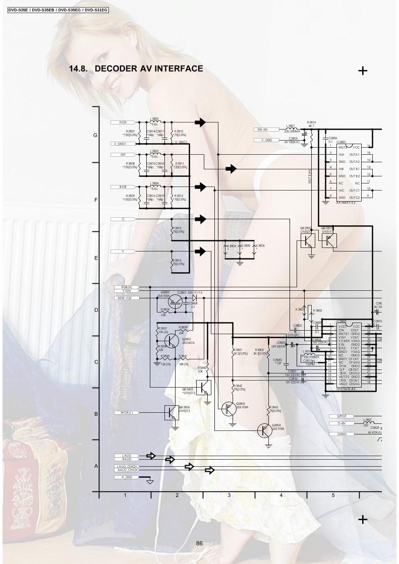
14.8. DECODER AV INTERFACE
WIDE(L )
NSW +12V
SW +5V
V _GND1
L AUD
S/PDI F
D+5V
DGND
G/Y
RGB (H)
RAUD
Y C(H)
C3825
6V 47(K A)
L AU D_CINCHRAU D_CINCH
L 3801
22U
A_GND
C3809
0.1
C38100.1
C3826V 100
C38
C383
Q38032SB 709A
Q38042SB 709A
QR3801U N5111
QR3802U N5213
Q38012SD601A
Q38022SB 709A
D3801 MA111-T X
R3804
10K
R3839
22K
R383710K (G)
R383822K
R3841
18K [G]
C38080.1
R3840
12K [G]
L 3807
22U /280MA
C38036V 100(K A )
MU T E1
INA2
GND3
INB4
GND5
NC6
INC7
GND8
OU T C29
OU T C110
NC11
OU T B 212
OU T B 113
OUT A214
OUT A115
V CC16
IC3801
B A7660FS-E2
C38060.1
MU
TE
(H)
L 3810
*10U /155MAC3813
*22P
B /CB
R3809*150[0.5%]
C
Y
R/CR
R3807*150[0.5%]
R3810*75[0.5%]
R3812*75[0.5%]
R381575[0.5%]
R381675[0.5%]
QR3803*U N5213
R384510K
C383416V 22(K A )
C3802
0.01u[K ]
R38013K 3[0.5%]
R38023K 3[0.5%]
R384275[0.5%]
R384375[0.5%]
L 3802
*5.6u
L 3803
*5.6u
L 3804
*5.6u
R3811*75[0.5%]
V CC11
CIN2
MU T E13
V IN14
Y C-MIX5
Y IN6
B IAS7
GND18
NC9
GND110
NC11
CY IN12
CL P13
MU T E215
CRIN16
GND217
CB IN14
CRSAG18
CROU T19
GND220
CB SAG21
CB OU T22
GND223
CY SAG24
GND226
Y SAG27
Y OU T28
GND229
V SAG30
V OU T31
GND232
COU T33
V CC34
CY OU T25
IC3803
MM1567B JB E
K 3802*
K 3803
C383216V 22(SW )
C383316V 22(SW )
C383116V 22(SW )
R3808*150[0.5%]
C3814*68p
C3817*68p
C3815*68p
C3818*68p
C3816*68p
C3819*68p
QR3804U N5213
R38144K 7
V _GND1V _GND
C3830*12P
K 3804*
K 3805*
K 3806*
F
G
E
D
C
B
A
54321
+
+
DVD-S35E / DVD-S35EB / DVD-S35EG / DVD-S31EG
86
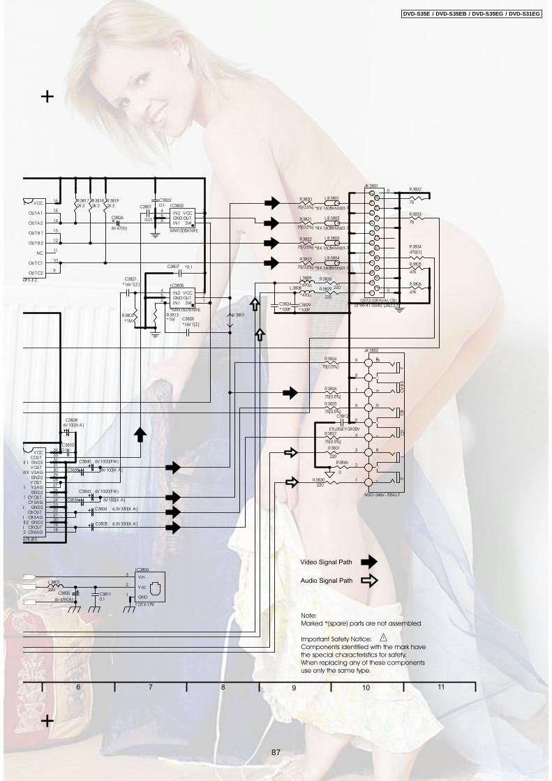
F
D
C38110.1
R3833
75
R3829
220
R3828
220
R3834
470[D]
L 3809
*470uL 3808
*470u
C3825
6V 47(K A)
R3831
220
R3830220
L 3801
22U
C3829*100P
R3805
47K
R3806
47K
SW1
OU T2
V CC3
IN24
GND5
IN16
IC3802
MM1505X NRE
C3801
0.01
C38100.1
C38286V 100[K A]
C3835 6V 100[K A ]
C3836 6V 100[K A ]
E
OU T C29
OU T C110
NC11
OU T B 212
OU T B 113
OUT A214
OUT A115
V CC16
60FS-E2
R38172K 2
R38182K 2
R38192K 2
C38220.1
C3812
ERJ3GEY 0R00V
N
C3826
6V 47(N)
R3832
75
C3824
*100P
C3843 6V 1000(FW )
C3840 6V 1000(FW )
C3804 6,3V 330[K A ]
C3805 6,3V 330[K A ]
R3846
0
L B 3801
*B K 1608HM601-T
L B 3802
*B K 1608HM601-T
L B 3803
*B K 1608HM601-T
L B 3804
*B K 1608HM601-T
V in3
V cc2
GND1
IC3804
T OT X 179
1
E1
MIX
1
1
N
E2N2
N
CRSAG18
CROU T19
GND220
CB SAG21
CB OU T22
GND223
CY SAG24
GND226
Y SAG27
Y OU T28
GND229
V SAG30
V OU T31
GND232
COU T33
V CC34
CY OU T25
3
67B JB E
SW1
OU T2
V CC3
IN24
GND5
IN16
IC3805
*MM1507X NREK 3801R3803
*1M
R3813*1M
1 3
5 7
91
11
31
51
71
92
12
01
81
61
41
21
0 8
6 4
2 0
0JK 3801
12012 (GRAVAL OS)or YKF41-5040 (JALCO)
R3820
75[0.5%]
R3821
75[0.5%]
R3822
75[0.5%]
R3823
75[0.5%]
R3824
75[0.5%]
R3826
75[0.5%]
R3825
75[0.5%]
R3827
75[0.5%]
C3821
*16V 1[Z ]
C3820
*16V 1[Z ]
C3807 *0.1
YC
RC
B
3
CV
BS
2
1
6
5
4
LR
9
8
7
rw
rb
ygn
JK 3802
MSD-246V -70NI L F
!
Note: Marked *(spare) parts are not assembled
Important Safety Notice:Components identified with the mark have the special characteristics for safety.When replacing any of these components use only the same type.
Audio Signal Path
Video Signal Path
8 9 1076 11
+
+
DVD-S35E / DVD-S35EB / DVD-S35EG / DVD-S31EG
87
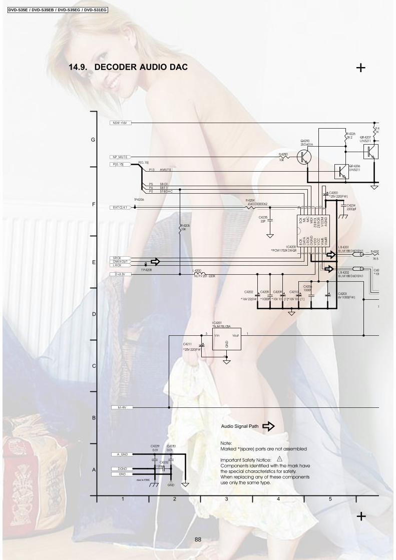
14.9. DECODER AUDIO DAC
SRCKDMIX OU T
EX T CL K 1
L RCK
A_GND
DGND
D+3.3V
NSW +16V
QR4206U N5211
R42262K 2 QR4207
U N5211
C4205
*1000P
C42061000P
C420*100
C4209
*10V 10 - [T ]
C4210
*10V 10 - [T ]
C4229
0.01
BC
K1
DA
TA
2
LR
CK
3
DG
ND
4M
DI
13
MC
14
ML
15
SC
K16
ZE
RO
L12
ZE
RO
R11
VC
OM
10
AG
ND
9
VD
D5
VC
C6
VoutL
7
VoutR
8
I C4200*PCM1752K DB QR
P[0..15]
P5P6
SB O1SB T 1
P0 ST B DAC
P13 AMU T E
P[0..15]
GND
GND
C4230
0.01
M+9V
NP_MU T E
Q42902SD601A
R4290
10K
C42342200pF
T P4208
TP4206 R4204J0JCC0000062
R41K
C4200*25V 220(FW )
C42036V 1000(FW )
Vout1
V in3
GN
D2
IC4201*NJM78L 05A
C4211
*25V 220(FW )
L B 4202B L M18B D601SN1
L B 4201B L M18B D601SN1
L 4200
NL FV 25T -220K
C4202
*16V 22(SW )
C4235
22P
R420510K
due to EMC
C4232
120pF
R4200
7K 5
1
!
Note: Marked *(spare) parts are not assembled
Important Safety Notice:Components identified with the mark have the special characteristics for safety.When replacing any of these components use only the same type.
Audio Signal Path
F
G
E
D
C
B
A
54321
+
+
DVD-S35E / DVD-S35EB / DVD-S35EG / DVD-S31EG
88

NSW +12V
C42260.01
RAU D
R4223680
QR4206U N5211
R42262K 2 QR4207
U N5211
QR4200U N5111
Q42052SD601AR4236
820
Q42042SD601A
R4232680
R4235
820
RAU D_CINCH
R420247K
L 4201 *22U
L 420222U
C4207*1000P
C4208*1000P
L AU D
R4224680
Q42032SD601AR4233
820
Q42022SD601A
R4231680
R4234
820
L AU D_CINCH
R420147K
Q4201 2SD1996
D4201MA4130N-LT A
C421516V 47(K A)
R42071K [D]
SW +5V
NSW+5.6V
Q4206
2SD1996
C42180.01
Q4207 *2SD601A
C422810V 220 (K A )
D4202MA111-T X
V _GND
C42140.01
C42342200pF
TP4201
C4231*16V 47 - K A
R4208
1K 8[D]
R42271K 8[D]
W )
03000(FW )
C420425V 220(FW )
202M18B D601SN1
201M18B D601SN1
C42176V 47(K A)
C4212
6V 47(K A)
C4213
6V 47(K A)
OU T 11
IN1-2
IN1+3
V SS4
IN2+5
IN2-6
OU T 27
V DD8
IC4202
NJM4580ED-T 1
C420116V 22(SW )
C421616V 22(SW )
R4217
0 R4219
0
R4200
7K 5
R4215
7K 5
R4216
15K (0.5%)R4218
15K (0.5%)
C422182P
C422282P
D4203MA4051N-HT A
R420312K [2%]
R420624K [2%]
8 9 1076 11
+
+
DVD-S35E / DVD-S35EB / DVD-S35EG / DVD-S31EG
89

14.10. TERMINAL PCB
!
Note: Marked *(spare) parts are not assembled
Important Safety Notice:Components identified with the mark have the special characteristics for safety.When replacing any of these components use only the same type.
F
G
E
D
C
B
A
54321 6
DVD-S35E / DVD-S35EB / DVD-S35EG / DVD-S31EG
90


