

VORAGO Tech Brief
Page 1
RADIATION HARDENED SYSTEM CONTROL BOARD FOR CUBESATS
THE CHALLENGE
CubeSats are very popular and growing in importance to
fulfill more and more commercial space missions. The
bulk of the ready-to-use CPU cards for the CubeSat
market use commercial-off-the-shelf (COTS)
semiconductor devices. While these have been shown to
be at times sufficient up to 10 kRads, more and more
missions are experiencing higher levels of radiation over
their life span than COTs devices can survive or reliably
operate. There have also been reports of devices
exhibiting latch-up susceptibility to single event effects
such as high energy neutron or proton strikes.
The challenge is to provide a cost-effective radiation
hardened system control board / compute module that can
be used in the standard form factor of CubeSat modules.
THE SOLUTION
VORAGO Technologies partnered with COSMIAC (a
University of New Mexico research center), based on the
expertise they bring in reconfigurable microsystems and
the history they have in CubeSat electronics and radiation
effects for spacecraft, to create a hardened compute
module. The module is called “HARDSAT Compute
Module” in reference to the underlying VORAGO
technologies’ silicon process used to combat ill effects of
radiation.
The HARDSAT compute module (CM) and associated
board stack were developed to allow rapid development, a
high degree of configurability, a small form factor and a
highly robust system for small satellite applications.
VORAGO Technologies already has proven radiation
hardened ARM® Cortex®-M0 based Microcontroller
Units (MCUs). The latest VORAGO Technologies’
MCU with 128kbytes of code space is used for this
project. It is envisioned that future modules using the
same form factor and interconnect can include higher
performance MCUs with more available memory. A
compute module and an interface board to the CubeSat kit
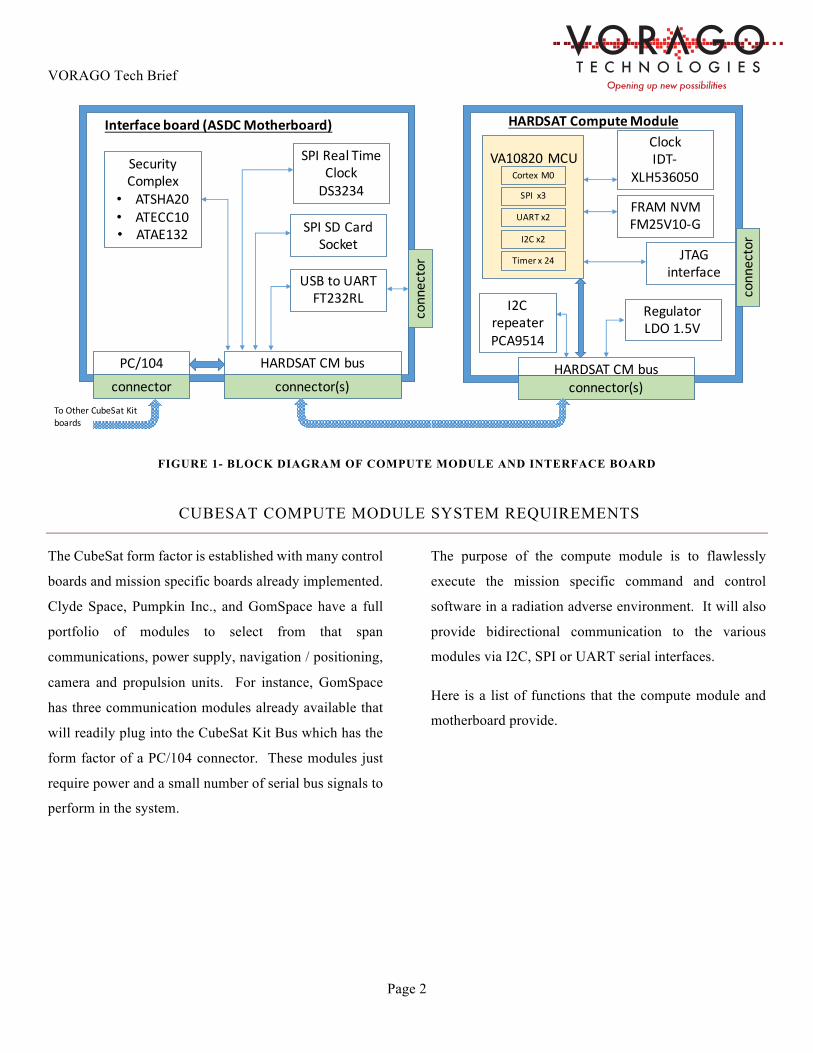
bus was developed and prototyped. See Figure 1 for
block diagrams of both boards. The rest of this brief
provides more details of the solution.
VORAGO Tech Brief
Page 2
FIGURE 1- BLOCK DIAGRAM OF COMPUTE MODULE AND INTERFACE BOARD
CUBESAT COMPUTE MODULE SYSTEM REQUIREMENTS
The CubeSat form factor is established with many control
boards and mission specific boards already implemented.
Clyde Space, Pumpkin Inc., and GomSpace have a full
portfolio of modules to select from that span
communications, power supply, navigation / positioning,
camera and propulsion units. For instance, GomSpace
has three communication modules already available that
will readily plug into the CubeSat Kit Bus which has the
form factor of a PC/104 connector. These modules just
require power and a small number of serial bus signals to
perform in the system.
The purpose of the compute module is to flawlessly
execute the mission specific command and control
software in a radiation adverse environment. It will also
provide bidirectional communication to the various
modules via I2C, SPI or UART serial interfaces.
Here is a list of functions that the compute module and
motherboard provide.
SPIRealTimeClockDS3234
SPISDCardSocket
USBtoUARTFT232RL
ClockIDT-
XLH536050
RegulatorLDO1.5V
JTAGinterface
SecurityComplex• ATSHA20• ATECC10• ATAE132
FRAMNVMFM25V10-G
PC/104 HARDSATCMbus HARDSATCMbus
VA10820MCUCortexM0
SPI x3
UARTx2
I2Cx2
Timerx24
I2CrepeaterPCA9514
connector(s)connector
connector
connector(s)
connector
ToOtherCubeSatKitboards
Interfaceboard(ASDCMotherboard) HARDSATComputeModule

VORAGO Tech Brief
Page 3
Category Compute Mod Motherboard
Processor 50 MHz,
Cortex®-M0® None
Memory 128k SPI
FRAM SD Card
Security None SHA and RNG
Timers 24 – 32-bit
timers
RTC with
battery
Serial
interfaces
2 x I2C, 3 x
SPI, 2 x UART
USB to UART
converter
TABLE 1- LIST OF FUNCTIONS FOR THE COMPUTE MODULE AND MOTHERBOARD
IMPLEMENTATION STRATEGY
The main purpose of this project was to provide satellite
developers with a scalable and cost-effective radiation
hardened compute module for small satellite projects.
VORAGO Technologies already has proven radiation
hardened Cortex M0-based MCUs. The latest version
with 128kbyte of program space is used in this project.
The dimensions of the compute module were selected to
sit inside the cube satellite chassis to allow both a means
to connect to the CubeSat PC/104 bus and have its own
set of board-to-board connections allowing stacking of
either compute modules or yet to be developed
application specific daughter cards (ASDC). The first
ASDC contains an SD memory card, a security platform
for encryption and authentication, a real-time clock and a
connector for interfacing a to the CubeSat Kit bus. It is
referred to as a “motherboard” since it replaces much of
the Pumpkin CubeSat motherboard.
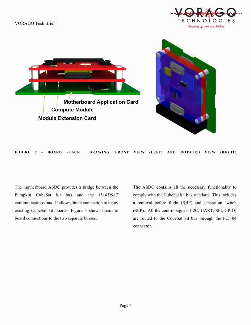
See Figure 2 for a drawing of the board stack.
VORAGO Tech Brief
Page 4
FIGURE 2 - BOARD STACK DRAWING, FRONT VIEW (LEFT) AND ROTATED VIEW (RIGHT)
The motherboard ASDC provides a bridge between the
Pumpkin CubeSat kit bus and the HARDSAT
communications bus. It allows direct connection to many
existing CubeSat kit boards. Figure 3 shows board to
board connections to the two separate busses.
The ASDC contains all the necessary functionality to
comply with the CubeSat kit bus standard. This includes
a removal before flight (RBF) and separation switch
(SEP). All the control signals (I2C, UART, SPI, GPIO)
are routed to the CubeSat kit bus through the PC/104
connector.
VORAGO Tech Brief
Page 5
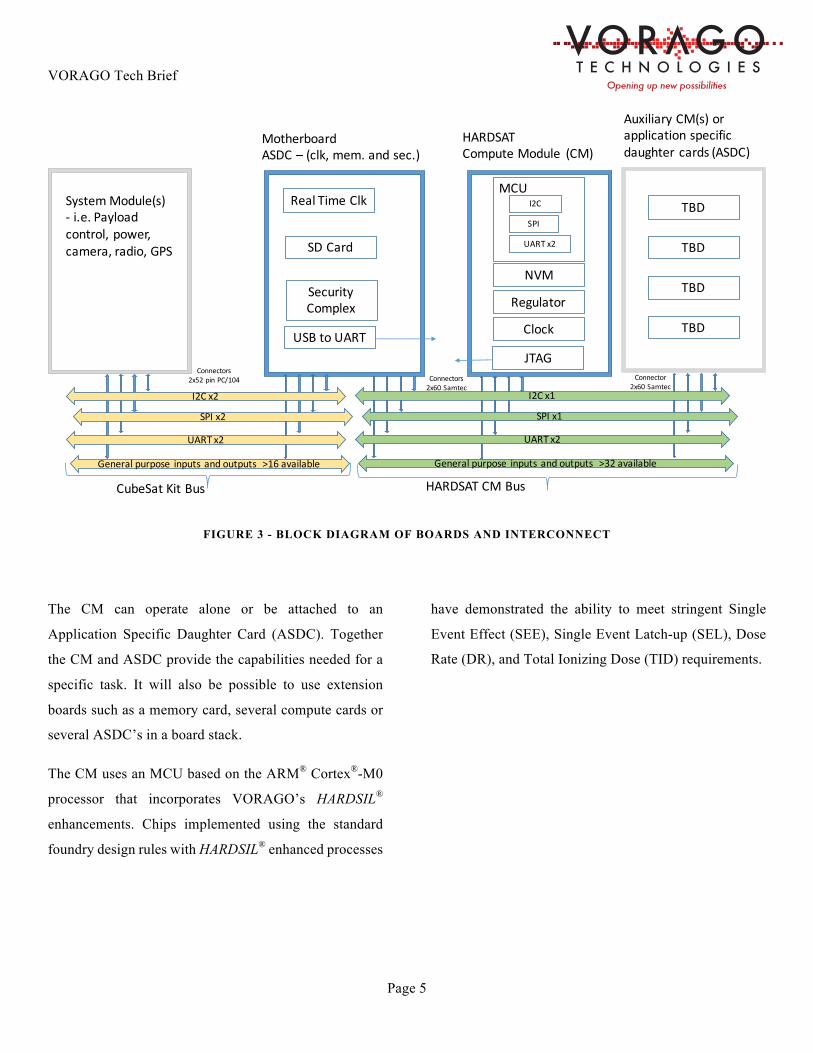
FIGURE 3 - BLOCK DIAGRAM OF BOARDS AND INTERCONNECT
The CM can operate alone or be attached to an
Application Specific Daughter Card (ASDC). Together
the CM and ASDC provide the capabilities needed for a
specific task. It will also be possible to use extension
boards such as a memory card, several compute cards or
several ASDC’s in a board stack.
The CM uses an MCU based on the ARM® Cortex®-M0
processor that incorporates VORAGO’s HARDSIL®
enhancements. Chips implemented using the standard
foundry design rules with HARDSIL® enhanced processes
have demonstrated the ability to meet stringent Single
Event Effect (SEE), Single Event Latch-up (SEL), Dose
Rate (DR), and Total Ionizing Dose (TID) requirements.
HARDSATCMBus
SystemModule(s)- i.e.Payloadcontrol,power,camera,radio,GPS
MotherboardASDC– (clk,mem.andsec.)
HARDSATComputeModule (CM)
AuxiliaryCM(s)orapplicationspecificdaughtercards(ASDC)
RealTimeClk
SDCard
USBtoUART
MCUTBD
Clock
Regulator
JTAG
TBD
TBD
TBD
Connectors2x52pinPC/104 Connectors
2x60Samtec
SecurityComplex
I2C
SPI
UARTx2
I2Cx1
SPIx1
UARTx2
Generalpurpose inputs andoutputs >32available
Connector2x60Samtec
NVM
I2Cx2
SPIx2
UARTx2
Generalpurpose inputs andoutputs >16available
CubeSatKitBus

VORAGO Tech Brief
Page 6
INNOVATION
The key innovations of this program relating to the
Compute module are listed here.
• Allows for state-of-the-art commercial firmware and
software to be used without the additional expense of
coding for radiation effects.
• Reduces development time and cost given the CM
uses standard interfaces that are well understood
(I2C, SPI and UART).
• Describes the connector pin out which provides both
pass-through signals and unique card identification
depending on the position of the board in the stack.
• The CM allows for the developer to quickly adapt
current designs to a more robust radiation hardened
platform.
• Reduces the dependency on decades old radiation
hardened parts.
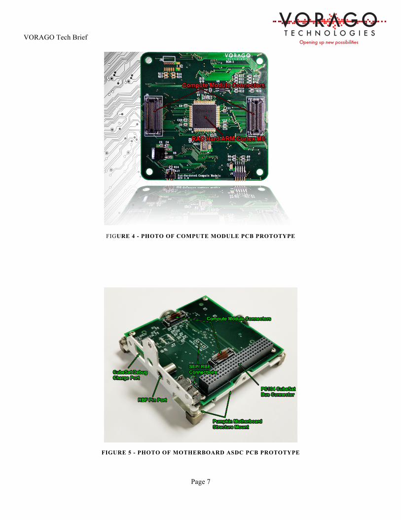
PROTOTYPE RESULTS
Figure 4 shows the functioning prototype of the compute
modules. Figure 5 shows the functioning motherboard.
Software was developed to communicate with the
peripheral chips on the I2C, SPI and UART interfaces.
This software was further refined and is now available as
part of the board support package for the REB1
development board that can be found at:
http://www.voragotech.com/products/reb1. Application
notes with software for FreeRTOS, timers and SPI
examples can be found at
http://www.voragotech.com/resources
VORAGO Tech Brief
Page 7
FIGURE 4 - PHOTO OF COMPUTE MODULE PCB PROTOTYPE
FIGURE 5 - PHOTO OF MOTHERBOARD ASDC PCB PROTOTYPE
VORAGO Tech Brief
Page 8
SUMMARY
As the CubeSat markets and their applications increase,
the need for similar components will continue to increase
to keep these projects affordable. This implementation
leverages the similarities in most CubeSats by applying a
modular approach to the spacecraft main electronics, the
motherboard.
The real power of this modular design concept is in giving
the engineer a wide variety of design options with a single
development environment. The motherboard is not the
only component in a spacecraft. By providing a CM that
is self-contained and has a standard interface, the
engineer can add a radiation hardened, secure, and robust
computation element to any subsystem or payload. The
only requirement is connecting a CM to an ASDC that
was created for the subsystem. In addition, the cost and
time to develop a new subsystem is greatly reduced since
manufacturing costs for the CM will decrease as more
units are fabricated per run. The cost and development
time of the ASDCs will also be reduced since the ASDC
will be designed to route the connections of the CM that
are needed. There is really no limit to what system can
take advantage of the CMs features.
This modular approach allows for a radiation hardened
single development environment for any size project. For
example, a CM can provide a radiation hardened
computation solution for an attitude control system
ASDC, or an electrical power system ASDC. This
modular approach shall significantly reduce development
time and increase reliability.
VORAGO TECHNOLOGIES INFORMATION
Address: 1501 South MoPac Expressway
Suite 350
Austin, TX 78746
Phone: (512) 633-7992
Email: [email protected]
VORAGO Tech Brief
Page 9
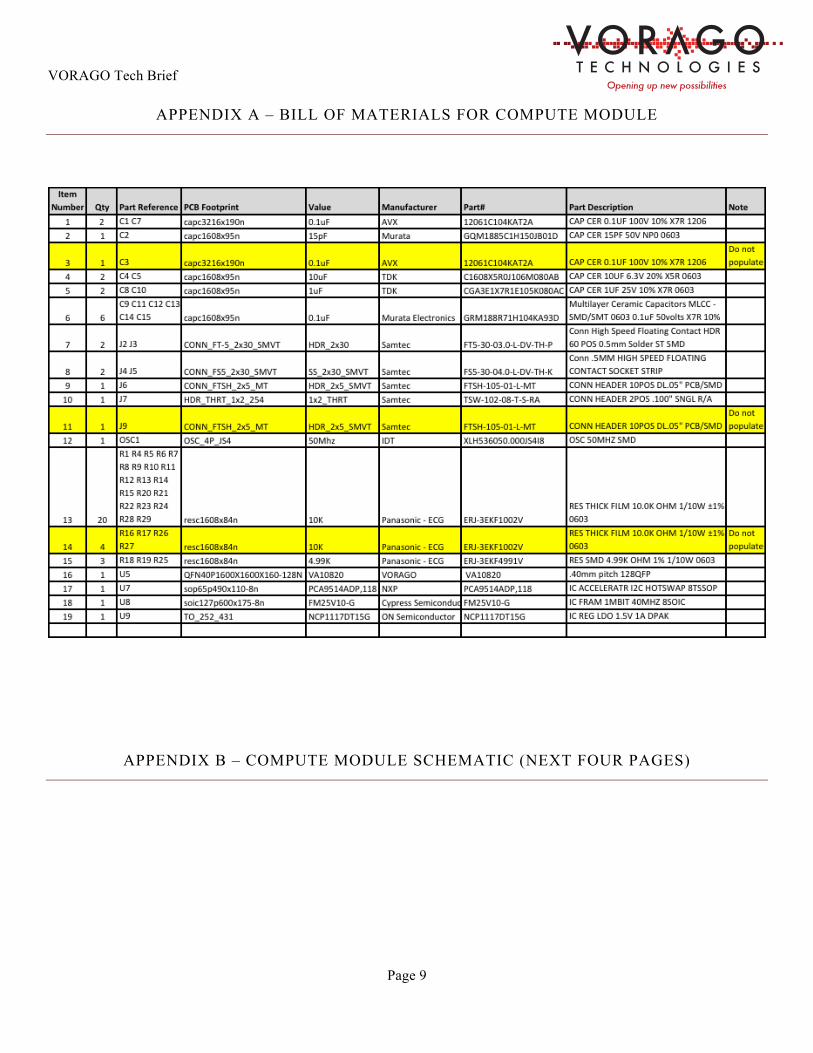
APPENDIX A – BILL OF MATERIALS FOR COMPUTE MODULE
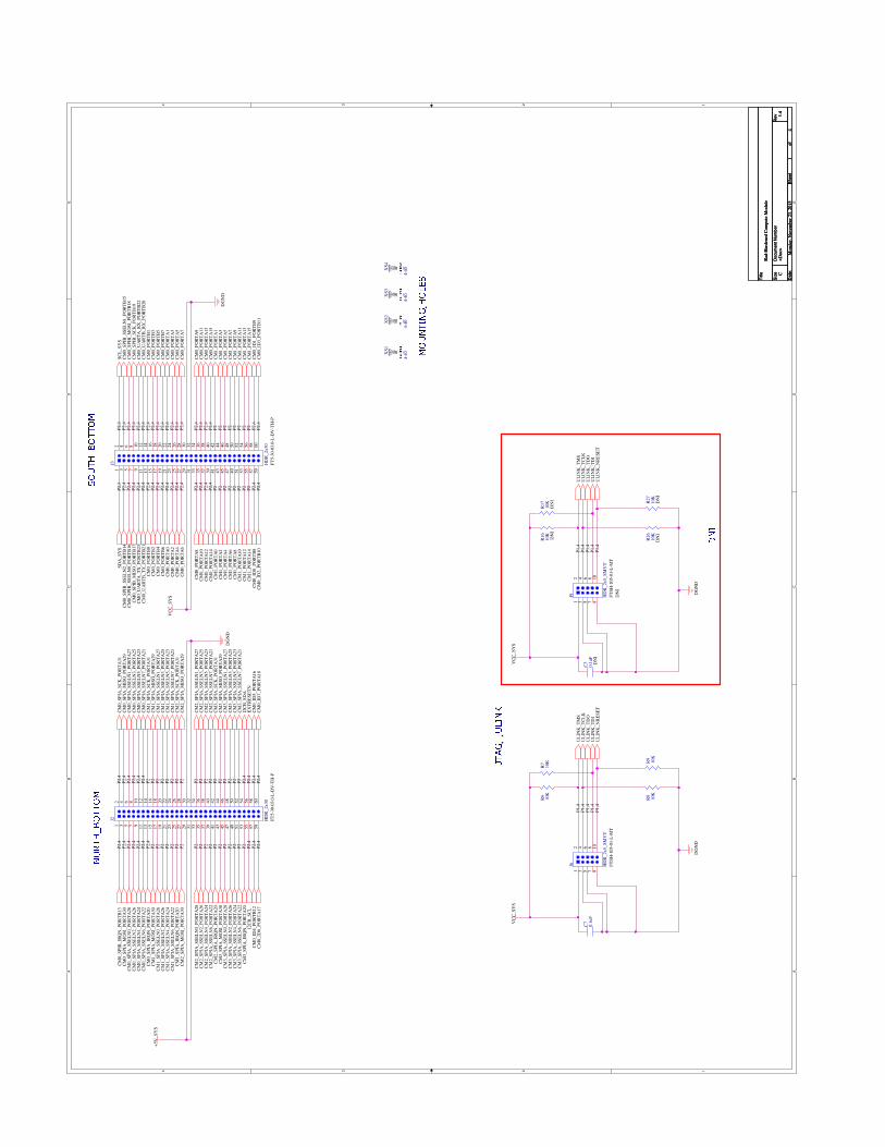
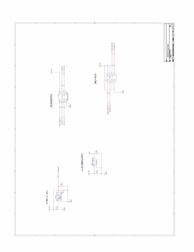
APPENDIX B – COMPUTE MODULE SCHEMATIC (NEXT FOUR PAGES)
A A
B B
C C
D D
E E
44
33
22
11
CM0_
SPIB
_SSE
LN2_
PORT
B14
P2,4
CM0_
SPIB
_SSE
LN1_
PORT
B15
P2,4
CM0_
SPIB
_SSE
LN0_
PORT
B16
P2,4
CM0_
SPIB
_MO
SI_P
ORT
B18
P2,4
CM0_
SPIB
_MIS
O_P
ORT
B17
P2,4
CM0_
UA
RTA
_TX
_PO
RTB2
3P2
,4CM
0_U
ART
B_TX
_PO
RTB2
1P2
,4CM
0_PO
RTB0
P2,4
CM0_
PORT
B2P2
,4CM
0_PO
RTB4
P2,4
CM0_
PORT
B6P2
,4CM
0_PO
RTA
0P2
,4CM
0_PO
RTA
2P2
,4CM
0_PO
RTA
4P2
,4CM
0_PO
RTA
6P2
,4
CM0_
PORT
A8
P2,4
CM0_
PORT
A10
P2,4
CM0_
PORT
A12
P2,4
CM0_
PORT
A14
P2,4
CM1_
PORT
A0
P2CM
1_PO
RTA
2P2
CM1_
PORT
A4
P2CM
1_PO
RTA
6P2
CM1_
PORT
A8
P2CM
1_PO
RTA
10P2
CM1_
PORT
A12
P2CM
1_PO
RTA
14P2
CM0_
ID0_
PORT
B8P2
,4
CM0_
SPIB
_SCK
_PO
RTB1
9P2
,4CM
0_U
ART
A_R
X_P
ORT
B22
P2,4
CM0_
UA
RTB_
RX_P
ORT
B20
P2,4
CM0_
PORT
B1P2
,4CM
0_PO
RTB3
P2,4
CM0_
PORT
B5P2
,4CM
0_PO
RTB7
P2,4
CM0_
PORT
A1
P2,4
CM0_
PORT
A3
P2,4
CM0_
PORT
A5
P2,4
CM0_
PORT
A7
P2,4
CM0_
PORT
A9
P2,4
CM0_
PORT
A11
P2,4
CM0_
PORT
A13
P2,4
CM0_
PORT
A15
P2,4
CM1_
PORT
A1
P2CM
1_PO
RTA
3P2
CM1_
PORT
A5
P2CM
1_PO
RTA
7P2
CM1_
PORT
A9
P2CM
1_PO
RTA
11P2
CM1_
PORT
A13
P2CM
1_PO
RTA
15P2
CM0_
ID1_
PORT
B9P2
,4
CM0_
SPIA
_MO
SI_P
ORT
A30
P2,4
CM0_
SPIA
_SSE
LN0_
PORT
A28
P2,4
CM0_
SPIA
_SSE
LN2_
PORT
A26
P2,4
CM0_
SPIA
_SSE
LN4_
PORT
A24
P2,4
CM0_
SPIA
_SSE
LN6_
PORT
A22
P2,4
CM0_
SPIA
_IRQ
N_P
ORT
A20
P2,4
CM1_
SPIA
_MO
SI_P
ORT
A30
P2CM
1_SP
IA_S
SELN
0_PO
RTA
28P2
CM1_
SPIA
_SSE
LN2_
PORT
A26
P2CM
1_SP
IA_S
SELN
4_PO
RTA
24P2
CM1_
SPIA
_SSE
LN6_
PORT
A22
P2CM
1_SP
IA_I
RQN
_PO
RTA
20P2
CM2_
SPIA
_MO
SI_P
ORT
A30
P2
CM2_
SPIA
_SSE
LN0_
PORT
A28
P2CM
2_SP
IA_S
SELN
2_PO
RTA
26P2
CM2_
SPIA
_SSE
LN4_
PORT
A24
P2CM
2_SP
IA_S
SELN
6_PO
RTA
22P2
CM2_
SPIA
_IRQ
N_P
ORT
A20
P2CM
3_SP
IA_M
OSI
_PO
RTA
30P2
CM3_
SPIA
_SSE
LN0_
PORT
A28
P2CM
3_SP
IA_S
SELN
2_PO
RTA
26P2
CM3_
SPIA
_SSE
LN4_
PORT
A24
P2CM
3_SP
IA_S
SELN
6_PO
RTA
22P2
CM3_
SPIA
_IRQ
N_P
ORT
A20
P2I2
CB_S
CLP2
,4CM
0_ID
4_PO
RTB1
2P2
,4CM
0_ID
5_PO
RTA
16P2
,4EX
TRES
ETN
P2,4
I2CB
_SD
AP2
,4CM
3_SP
IA_S
SELN
7_PO
RTA
21P2
CM3_
SPIA
_SSE
LN5_
PORT
A23
P2CM
3_SP
IA_S
SELN
3_PO
RTA
25P2
CM3_
SPIA
_SSE
LN1_
PORT
A27
P2CM
3_SP
IA_M
ISO
_PO
RTA
29P2
CM3_
SPIA
_SCK
_PO
RTA
31P2
CM2_
SPIA
_SSE
LN7_
PORT
A21
P2CM
2_SP
IA_S
SELN
5_PO
RTA
23P2
CM2_
SPIA
_SSE
LN3_
PORT
A25
P2CM
2_SP
IA_S
SELN
1_PO
RTA
27P2
CM2_
SPIA
_MIS
O_P
ORT
A29
P2CM
2_SP
IA_S
CK_P
ORT
A31
P2CM
1_SP
IA_S
SELN
7_PO
RTA
21P2
CM1_
SPIA
_SSE
LN5_
PORT
A23
P2CM
1_SP
IA_S
SELN
3_PO
RTA
25P2
CM1_
SPIA
_SSE
LN1_
PORT
A27
P2CM
1_SP
IA_M
ISO
_PO
RTA
29P2
CM1_
SPIA
_SCK
_PO
RTA
31P2
CM0_
SPIA
_SSE
LN7_
PORT
A21
P2,4
CM0_
SPIA
_SSE
LN5_
PORT
A23
P2,4
CM0_
SPIA
_SSE
LN3_
PORT
A25
P2,4
CM0_
SPIA
_SSE
LN1_
PORT
A27
P2,4
CM0_
SPIA
_MIS
O_P
ORT
A29
P2,4
SDA
_SY
SP2
,3SC
L_SY
SP2
,3
CM0_
ID2_
PORT
B10
P2,4
CM0_
ID3_
PORT
B11
P2,4
CM0_
SPIB
_IRQ
N_P
ORT
B13
P2,4
CM0_
SPIA
_SCK
_PO
RTA
31P2
,4
CM0_
ID6_
PORT
A17
P2,4
CM0_
ID7_
PORT
A18
P2,4
ULI
NK
_TM
SP1
,4U
LIN
K_T
CLK
P1,4
ULI
NK
_TD
OP1
,4U
LIN
K_T
DI
P1,4
ULI
NK
_NRE
SET
P1,4
ULI
NK
_TM
SP1
,4U
LIN
K_T
CLK
P1,4
ULI
NK
_TD
OP1
,4U
LIN
K_T
DI
P1,4
ULI
NK
_NRE
SET
P1,4
DG
ND
DG
ND
VCC
_SY
S
+5V
_SY
S
VCC
_SY
S
DG
ND
VCC
_SY
S
DG
ND
Title
Size
Doc
umen
t Num
ber
Rev
Dat
e:Sh
eet
of
<Doc
>1.
4
Rad-
Har
dene
d Co
mpu
te M
odul
e
C
14
Mon
day,
Nov
embe
r 23,
201
5
Title
Size
Doc
umen
t Num
ber
Rev
Dat
e:Sh
eet
of
<Doc
>1.
4
Rad-
Har
dene
d Co
mpu
te M
odul
e
C
14
Mon
day,
Nov
embe
r 23,
201
5
Title
Size
Doc
umen
t Num
ber
Rev
Dat
e:Sh
eet
of
<Doc
>1.
4
Rad-
Har
dene
d Co
mpu
te M
odul
e
C
14
Mon
day,
Nov
embe
r 23,
201
5
J2 HD
R_2x
30FT
5-30
-03.
0-L-
DV
-TH
-P
1 32 4
56
78
9 1110 12
13 15 17 19 21 25
14 16 18 20 22 24 2623
2827 29
3031
3233
3435 37 39 41 43
36 38 40 42 4445 47 49 51 53 55 57 59
46 48 50 52 54 56 58 60 R8 10K
R26
10K
DN
I
C7 0.1u
FC3 0.
1uF
DN
I
XS1
4-40
XS2
4-40
R7 10K
J6 HD
R_2x
5_SM
VT
FTSH
-105
-01-
L-M
T
1 32 4
56
78
910
R17
10K
DN
I
XS3
4-40
R6 10K
R16
10K
DN
I
J3 HD
R_2x
30FT
5-30
-03.
0-L-
DV
-TH
-P
1 32 4
56
78
9 1110 12
13 15 17 19 21 25
14 16 18 20 22 24 2623
2827 29
3031
3233
3435 37 39 41 43
36 38 40 42 4445 47 49 51 53 55 57 59
46 48 50 52 54 56 58 60
XS4
4-40
R9 10K
J9 HD
R_2x
5_SM
VT
FTSH
-105
-01-
L-M
TD
NI
1 32 4
56
78
910
R27
10K
DN
I

A A
B B
C C
D D
E E
44
33
22
11
Rev
isio
ns:
1.0
- Cre
ated
Sch
emat
ic1.
1 - C
hang
ed 5
K to
4.9
K1.
2 - R
emov
ed o
ne E
FUSE
1.3
- DN
I JTA
G (o
ne)
1.4
- Add
2 0
.1uf
on
1.5V
and
3.3
V (V
CC
_SYS
)
CM1_
PORT
A6
P1CM
1_PO
RTA
7P1
CM1_
PORT
A8
P1CM
1_PO
RTA
9P1
CM1_
PORT
A10
P1CM
1_PO
RTA
11P1
CM1_
PORT
A12
P1CM
1_PO
RTA
13P1
CM1_
PORT
A14
P1CM
1_PO
RTA
15P1
CM0_
PORT
A0
P1,4
CM0_
PORT
A1
P1,4
CM0_
PORT
A2
P1,4
CM0_
PORT
A3
P1,4
CM0_
PORT
A4
P1,4
CM0_
PORT
A5
P1,4
CM0_
PORT
A6
P1,4
CM0_
PORT
A7
P1,4
CM0_
PORT
A8
P1,4
CM0_
PORT
A9
P1,4
CM0_
PORT
A10
P1,4
CM0_
PORT
A11
P1,4
CM0_
PORT
A12
P1,4
CM0_
PORT
A13
P1,4
CM0_
PORT
A14
P1,4
CM0_
PORT
A15
P1,4
CM0_
ID1_
PORT
B9P1
,4CM
0_ID
2_PO
RTB1
0P1
,4
SDA
_SY
SP1
,3SC
L_SY
SP1
,3
CM0_
SPIB
_SSE
LN0_
PORT
B16
P1,4
CM0_
SPIB
_MO
SI_P
ORT
B18
P1,4
CM0_
SPIB
_MIS
O_P
ORT
B17
P1,4
CM0_
SPIB
_SCK
_PO
RTB1
9P1
,4
CM0_
ID3_
PORT
B11
P1,4
CM0_
ID4_
PORT
B12
P1,4
CM0_
SPIB
_IRQ
N_P
ORT
B13
P1,4
CM1_
SPIA
_SCK
_PO
RTA
31P1
CM0_
ID7_
PORT
A18
P1,4
CM0_
ID0_
PORT
B8P1
,4
TORC
H_E
FUSE
_BU
RN_E
NN
P2,4
CM1_
SPIA
_MO
SI_P
ORT
A30
P1CM
1_SP
IA_M
ISO
_PO
RTA
29P1
CM1_
SPIA
_SSE
LN0_
PORT
A28
P1CM
1_SP
IA_S
SELN
1_PO
RTA
27P1
CM1_
SPIA
_SSE
LN2_
PORT
A26
P1CM
1_SP
IA_S
SELN
3_PO
RTA
25P1
CM1_
SPIA
_SSE
LN4_
PORT
A24
P1CM
1_SP
IA_S
SELN
5_PO
RTA
23P1
CM1_
SPIA
_SSE
LN6_
PORT
A22
P1CM
1_SP
IA_S
SELN
7_PO
RTA
21P1
CM1_
SPIA
_IRQ
N_P
ORT
A20
P1CM
2_SP
IA_S
CK_P
ORT
A31
P1CM
2_SP
IA_M
OSI
_PO
RTA
30P1
CM2_
SPIA
_MIS
O_P
ORT
A29
P1CM
2_SP
IA_S
SELN
0_PO
RTA
28P1
CM2_
SPIA
_SSE
LN1_
PORT
A27
P1CM
2_SP
IA_S
SELN
2_PO
RTA
26P1
CM2_
SPIA
_SSE
LN3_
PORT
A25
P1CM
2_SP
IA_S
SELN
4_PO
RTA
24P1
CM2_
SPIA
_SSE
LN5_
PORT
A23
P1CM
2_SP
IA_S
SELN
6_PO
RTA
22P1
CM2_
SPIA
_SSE
LN7_
PORT
A21
P1CM
2_SP
IA_I
RQN
_PO
RTA
20P1
CM3_
SPIA
_SCK
_PO
RTA
31P1
CM3_
SPIA
_MO
SI_P
ORT
A30
P1CM
3_SP
IA_M
ISO
_PO
RTA
29P1
CM3_
SPIA
_SSE
LN0_
PORT
A28
P1CM
3_SP
IA_S
SELN
1_PO
RTA
27P1
CM3_
SPIA
_SSE
LN2_
PORT
A26
P1CM
3_SP
IA_S
SELN
3_PO
RTA
25P1
CM3_
SPIA
_SSE
LN4_
PORT
A24
P1CM
3_SP
IA_S
SELN
5_PO
RTA
23P1
CM3_
SPIA
_SSE
LN6_
PORT
A22
P1CM
3_SP
IA_S
SELN
7_PO
RTA
21P1
CM3_
SPIA
_IRQ
N_P
ORT
A20
P1CM
0_SP
IA_S
CK_P
ORT
A31
P1,4
CM0_
SPIA
_MO
SI_P
ORT
A30
P1,4
CM0_
SPIA
_MIS
O_P
ORT
A29
P1,4
CM0_
SPIA
_SSE
LN0_
PORT
A28
P1,4
CM0_
SPIA
_SSE
LN1_
PORT
A27
P1,4
CM0_
SPIA
_SSE
LN2_
PORT
A26
P1,4
CM0_
SPIA
_SSE
LN3_
PORT
A25
P1,4
CM0_
SPIA
_SSE
LN4_
PORT
A24
P1,4
CM0_
SPIA
_SSE
LN5_
PORT
A23
P1,4
CM0_
SPIA
_SSE
LN6_
PORT
A22
P1,4
CM0_
SPIA
_SSE
LN7_
PORT
A21
P1,4
CM0_
SPIA
_IRQ
N_P
ORT
A20
P1,4
I2CB
_SD
AP1
,4I2
CB_S
CLP1
,4EX
TRES
ETN
P1,4
CM0_
ID5_
PORT
A16
P1,4
CM0_
ID6_
PORT
A17
P1,4
CM0_
SPIB
_SSE
LN2_
PORT
B14
P1,4
CM0_
SPIB
_SSE
LN1_
PORT
B15
P1,4
CM0_
UA
RTA
_TX
_PO
RTB2
3P1
,4CM
0_U
ART
A_R
X_P
ORT
B22
P1,4
CM0_
UA
RTB_
TX_P
ORT
B21
P1,4
CM0_
UA
RTB_
RX_P
ORT
B20
P1,4
CM0_
PORT
B0P1
,4CM
0_PO
RTB1
P1,4
CM0_
PORT
B2P1
,4CM
0_PO
RTB3
P1,4
CM0_
PORT
B4P1
,4CM
0_PO
RTB5
P1,4
CM0_
PORT
B6P1
,4CM
0_PO
RTB7
P1,4
CM1_
PORT
A0
P1CM
1_PO
RTA
1P1
CM1_
PORT
A2
P1CM
1_PO
RTA
3P1
CM1_
PORT
A4
P1CM
1_PO
RTA
5P1
VCC
_SY
S
DG
ND
+5V
_SY
S
DG
ND
DG
ND
Title
Size
Doc
umen
t Num
ber
Rev
Dat
e:Sh
eet
of
<Doc
>1.
4
Rad-
Har
dene
d Co
mpu
te M
odul
e
C
24
Mon
day,
Nov
embe
r 23,
201
5
Title
Size
Doc
umen
t Num
ber
Rev
Dat
e:Sh
eet
of
<Doc
>1.
4
Rad-
Har
dene
d Co
mpu
te M
odul
e
C
24
Mon
day,
Nov
embe
r 23,
201
5
Title
Size
Doc
umen
t Num
ber
Rev
Dat
e:Sh
eet
of
<Doc
>1.
4
Rad-
Har
dene
d Co
mpu
te M
odul
e
C
24
Mon
day,
Nov
embe
r 23,
201
5
J4 SS_2
x30_
SMV
TFS
5-30
-04.
0-L-
DV
-TH
-K
1 32 4
56
78
9 1110 12
13 15 17 19 21 25
14 16 18 20 22 24 2623
2827 29
3031
3233
3435 37 39 41 43
36 38 40 42 4445 47 49 51 53 55 57 59
46 48 50 52 54 56 58 60
J5 SS_2
x30_
SMV
TFS
5-30
-04.
0-L-
DV
-TH
-K
1 32 4
56
78
9 1110 12
13 15 17 19 21 25
14 16 18 20 22 24 2623
2827 29
3031
3233
3435 37 39 41 43
36 38 40 42 4445 47 49 51 53 55 57 59
46 48 50 52 54 56 58 60
J7 1x2_
THRT
12
A A
B B
C C
D D
E E
44
33
22
11
I2CA
_SD
AP4
SDA
_SY
SP1
,2
I2CA
_SCL
P4
SCL_
SYS
P1,2
TORC
H_C
LKP4
BUF_
ENA
BLE
P4
TORC
H_R
OM
_CSN
P4
SDI0
_RO
M_S
IP4
SCK
0_RO
M_S
CKP4
SDO
0_RO
M_S
OP4
DG
ND
VCC
_SY
S
DG
ND
DG
ND
VCC
_SY
S
VCC
_SY
S
DG
ND
DG
ND
VCC
_SY
S+1
.5V
Title
Size
Doc
umen
t Num
ber
Rev
Dat
e:Sh
eet
of
<Doc
>1.
4
Rad-
Har
dene
d Co
mpu
te M
odul
e
C
34
Mon
day,
Nov
embe
r 23,
201
5
Title
Size
Doc
umen
t Num
ber
Rev
Dat
e:Sh
eet
of
<Doc
>1.
4
Rad-
Har
dene
d Co
mpu
te M
odul
e
C
34
Mon
day,
Nov
embe
r 23,
201
5
Title
Size
Doc
umen
t Num
ber
Rev
Dat
e:Sh
eet
of
<Doc
>1.
4
Rad-
Har
dene
d Co
mpu
te M
odul
e
C
34
Mon
day,
Nov
embe
r 23,
201
5
C2 15pF
U8
CSN
1
SO2
WPN
3
VSS
4SI
5SC
K6
HO
LDN
7V
DD
8
OSC
1
50M
hzX
LH53
6050
.000
JS4I
8
VD
D4
OU
T3
GN
D2
ED1
U7
PCA
9514
AD
P,11
8
EN1
SCLO
UT
2
SCLI
N3
GN
D4
VCC
8
SDA
OU
T7
SDA
IN6
RDY
5
U9
NCP
1117
DT1
5GO
UT
4IN
3
AD
J/GN
D1
C4 10uF
C1 0.1u
F
C5 10uF
R1 10K

A A
B B
C C
D D
E E
44
33
22
11
CM0_
PORT
B0P1
,2CM
0_PO
RTB1
P1,2
CM0_
PORT
B2P1
,2CM
0_PO
RTB3
P1,2
CM0_
PORT
B4P1
,2CM
0_PO
RTB5
P1,2
CM0_
PORT
B6P1
,2CM
0_PO
RTB7
P1,2
CM0_
ID0_
PORT
B8P1
,2CM
0_ID
1_PO
RTB9
P1,2
CM0_
ID2_
PORT
B10
P1,2
CM0_
ID3_
PORT
B11
P1,2
CM0_
ID4_
PORT
B12
P1,2
CM0_
SPIB
_IRQ
N_P
ORT
B13
P1,2
CM0_
SPIB
_SSE
LN2_
PORT
B14
P1,2
CM0_
SPIB
_SSE
LN1_
PORT
B15
P1,2
CM0_
SPIB
_SSE
LN0_
PORT
B16
P1,2
CM0_
SPIB
_MIS
O_P
ORT
B17
P1,2
CM0_
SPIB
_MO
SI_P
ORT
B18
P1,2
CM0_
SPIB
_SCK
_PO
RTB1
9P1
,2CM
0_U
ART
B_RX
_PO
RTB2
0P1
,2CM
0_U
ART
B_TX
_PO
RTB2
1P1
,2CM
0_U
ART
A_R
X_P
ORT
B22
P1,2
CM0_
UA
RTA
_TX
_PO
RTB2
3P1
,2
I2CA
_SCL
P3,4
I2CA
_SD
AP3
,4
I2CB
_SCL
P1,2
I2CB
_SD
AP1
,2
SCK
0_RO
M_S
CKP3
SDO
0_RO
M_S
OP3
TORC
H_R
OM
_CSN
P3,4
ULI
NK
_TD
OP1
TORC
H_C
LKP3
EXTR
ESET
NP1
,2
CM0_
PORT
A0
P1,2
CM0_
PORT
A1
P1,2
CM0_
PORT
A2
P1,2
CM0_
PORT
A3
P1,2
CM0_
PORT
A4
P1,2
CM0_
PORT
A5
P1,2
CM0_
PORT
A6
P1,2
CM0_
PORT
A7
P1,2
CM0_
PORT
A8
P1,2
CM0_
PORT
A9
P1,2
CM0_
PORT
A10
P1,2
CM0_
PORT
A11
P1,2
CM0_
PORT
A12
P1,2
CM0_
PORT
A13
P1,2
CM0_
PORT
A14
P1,2
CM0_
PORT
A15
P1,2
CM0_
ID5_
PORT
A16
P1,2
CM0_
ID6_
PORT
A17
P1,2
CM0_
SPIA
_IRQ
N_P
ORT
A20
P1,2
,4CM
0_SP
IA_S
SELN
7_PO
RTA
21P1
,2,4
CM0_
SPIA
_SSE
LN6_
PORT
A22
P1,2
,4CM
0_SP
IA_S
SELN
5_PO
RTA
23P1
,2,4
CM0_
SPIA
_SSE
LN4_
PORT
A24
P1,2
,4CM
0_SP
IA_S
SELN
3_PO
RTA
25P1
,2,4
CM0_
SPIA
_SSE
LN2_
PORT
A26
P1,2
,4CM
0_SP
IA_S
SELN
1_PO
RTA
27P1
,2,4
CM0_
SPIA
_SSE
LN0_
PORT
A28
P1,2
,4CM
0_SP
IA_M
ISO
_PO
RTA
29P1
,2,4
CM0_
SPIA
_MO
SI_P
ORT
A30
P1,2
,4CM
0_SP
IA_S
CK_P
ORT
A31
P1,2
,4
SDI0
_RO
M_S
IP3
ULI
NK
_TCL
KP1
ULI
NK
_TD
IP1
ULI
NK
_TM
SP1
ULI
NK
_NRE
SET
P1
TORC
H_E
FUSE
_BU
RN_E
NN
P2,4
TORC
H_D
STPO
RP4
CM0_
ID7_
PORT
A18
P1,2
BUF_
ENA
BLE
P3,4
I2CA_SDAP3,4
I2CA_SCLP3,4
CM0_SPIA_MISO_PORTA29P1,2,4
CM0_SPIA_SSELN0_PORTA28P1,2,4
CM0_SPIA_SSELN1_PORTA27P1,2,4
CM0_SPIA_SSELN2_PORTA26P1,2,4
CM0_SPIA_SSELN3_PORTA25P1,2,4
CM0_SPIA_SSELN4_PORTA24P1,2,4
CM0_SPIA_SSELN5_PORTA23P1,2,4
CM0_SPIA_SSELN6_PORTA22P1,2,4
CM0_SPIA_SSELN7_PORTA21P1,2,4
CM0_SPIA_IRQN_PORTA20P1,2,4
TORCH_EFUSE_BURN_ENNP2,4
TORCH_ROM_CSNP3,4
TORCH_DSTPORP4
CM0_SPIA_SCK_PORTA31P1,2,4
BUF_ENABLEP3,4
CM0_SPIA_MOSI_PORTA30P1,2,4
DG
ND
VCC
_SY
S
VCC
_SY
S
VCC
_SY
S
+1.5
VV
CC_S
YS
DG
ND
VCC
_SY
S+1
.5V
DG
ND
DG
ND Title
Size
Doc
umen
t Num
ber
Rev
Dat
e:Sh
eet
of
<Doc
>1.
4
Rad-
Har
dene
d Co
mpu
te M
odul
e
C
44
Mon
day,
Nov
embe
r 23,
201
5
Title
Size
Doc
umen
t Num
ber
Rev
Dat
e:Sh
eet
of
<Doc
>1.
4
Rad-
Har
dene
d Co
mpu
te M
odul
e
C
44
Mon
day,
Nov
embe
r 23,
201
5
Title
Size
Doc
umen
t Num
ber
Rev
Dat
e:Sh
eet
of
<Doc
>1.
4
Rad-
Har
dene
d Co
mpu
te M
odul
e
C
44
Mon
day,
Nov
embe
r 23,
201
5
C14
0.1u
FC1
20.
1uF
R4 10K
R19
4.99
KR1
210
K
R23
10K
C10
1uF
R15
10K
R13
10K
R24
10K
R25
4.99
K
R10
10K
C15
0.1u
FC1
30.
1uF
R20
10K
U5CL
K13
EXTR
ESET
N79
DST
POR
11
PORT
A[0
]90
PORT
A[1
]93
PORT
A[2
]10
4PO
RTA
[3]
105
PORT
A[4
]10
6
PORT
A[5
]10
7PO
RTA
[6]
109
PORT
A[7
]11
1PO
RTA
[8]
112
PORT
A[9
]11
3
PORT
A[1
0]11
5PO
RTA
[11]
116
PORT
A[1
2]11
7PO
RTA
[13]
118
PORT
A[1
4]12
0
PORT
A[1
5]12
2PO
RTA
[16]
123
PORT
A[1
7]12
4PO
RTA
[18]
126
PORT
A[1
9]15
PORT
A[2
0]17
PORT
A[2
1]19
PORT
A[2
2]23
PORT
A[2
3]25
PORT
A[2
4]38
PORT
A[2
5]40
PORT
A[2
6]41
PORT
A[2
7]42
PORT
A[2
8]43
PORT
A[2
9]45
PORT
A[3
0]47
PORT
A[3
1]48
ROM
_SI
77
TCK
6TD
I9
TMS
7TR
STN
8
EFU
SE_B
URN
_EN
N28
PORT
B[0]
49PO
RTB[
1]51
PORT
B[2]
52
PORT
B[3]
53PO
RTB[
4]54
PORT
B[5]
56PO
RTB[
6]58
PORT
B[7]
59
PORT
B[8]
60PO
RTB[
9]68
PORT
B[10
]98
PORT
B[11
]10
0PO
RTB[
12]
101
PORT
B[13
]10
2PO
RTB[
14]
127
PORT
B[15
]12
8PO
RTB[
16]
1PO
RTB[
17]
34
PORT
B[18
]36
PORT
B[19
]37
PORT
B[20
]62
PORT
B[21
]63
PORT
B[22
]64
PORT
B[23
]65
I2CA
_SCL
83I2
CA_S
DA
85
I2CB
_SCL
88I2
CB_S
DA
89
ROM
_SCK
70RO
M_S
O75
ROM
_CSN
72
TDO
5
VDD33_194 VDD33_1816 VDD33_1726 VDD33_1627 VDD33_1533 VDD33_1439 VDD33_1344 VDD33_1250 VDD33_1155 VDD33_1061 VDD33_967 VDD33_876 VDD33_786 VDD33_697 VDD33_5103 VDD33_4108 VDD33_3114 VDD33_2119
VDD33_1125
VDD15_918 VDD15_835 VDD15_746 VDD15_657 VDD15_569 VDD15_478 VDD15_399 VDD15_2110 VDD15_1121
VSS_272VSS_263VSS_25
10VSS_2412VSS_2314VSS_2220VSS_2121VSS_2022VSS_1924VSS_1829VSS_1730VSS_1631VSS_1532VSS_1466VSS_1371VSS_1273VSS_1174VSS_1080VSS_981VSS_882VSS_784VSS_687VSS_591VSS_492VSS_394VSS_295VSS_196
R29
10K
R21
10K
C9 0.1u
F
R18
4.99
K
C8 1uF
R14
10K
R28
10K
R22
10K
R11
10K
C11
0.1u
F
R5 10K


