

Reconfigurable RF Receiver Frontends for Multi-Standard Radios
by
Hossein Noori
A thesis submitted to the Graduate Faculty of
Auburn University
in partial fulfillment of the
requirements for the Degree of
Master of Science
Auburn, Alabama
May 9, 2011
Keywords: Reconfigurable Radio, Multi-Standard Radio, Receiver Frontend,
Multiband Radio, Low-Noise Amplifier (LNA), Noise Cancellation
Copyright 2011 by Hossein Noori
Approved by
Fa Foster Dai, Chair, Professor of Electrical and Computer Engineering
Richard C. Jaeger, Professor of Electrical and Computer Engineering
Bogdan M. Wilamowski, Professor of Electrical and Computer Engineering

ii
Abstract
Several Wireless Communication Standards have been developed over the past few
decades to address the growing and varying needs of the users. For example, while cellular
access technologies such as GSM and CDMA have satisfied the Wide-Area needs for voice and
moderate-speed data communication, the IEEE 802.11 series of standards have satisfied the
Local-Area demands for high-speed network access. Furthermore, the ability to establish a
Private-Area Network (PAN) has been made possible by the introduction of the Bluetooth
standard.
While these and other wireless standards were individually developed and optimized for a
specific need, the users expect most, if not all, of them to be incorporated and available to them
on a single device; i.e., their handsets. To fulfill this requirement, a new approach to the design
of Radio-Frequency (RF) receivers and transmitters shall be adopted in order to accommodate
the current and have the capability of handling the future wireless standards.
This document presents the review of current state-of-the-art Multi-Standard Receiver
Frontend architectures as well as the Design, Analysis, and Simulation results for a
Reconfigurable Multi-standard CMOS Low-Noise Amplifier (LNA) covering the DCS1800,
PCS1900, AWS1700, and IMT2100 frequency bands; utilizing positive feedback to improve
gain and provide flexibility in input power matching [5], cross-coupling noise cancellation
technique [6], and on-chip transistor-based current source. The simulation has been carried out
using a 0.12µm CMOS technology and Cadence’s Virtuoso Spectre simulation software.
iii
Acknowledgments
I would like to express my sincere gratitude to Dr. Fa Foster Dai, my academic advisor,
for his instrumental support and encouragement as well as insightful instructions from the
inception to the completion of this work. His directions at various stages of this effort were
crucial in overcoming the hurdles and entertaining other ideas for the purpose of enhancement of
the design and creation of a fruitful outcome.
I would also like to thank my committee members, Dr. Richard C Jaeger and Dr. Bogdan
M. Wilamowski, for their gracious support and discussions.
Finally, I would like to extend a special thank to Mr. Feng Zhao for providing an
opportunity for productive technical discussions at various phases of the design.
iv
Table of Contents
Abstract ........................................................................................................................................... ii
Acknowledgments.......................................................................................................................... iii
List of Tables ................................................................................................................................ vii
List of Figures .............................................................................................................................. viii
List of Abbreviations ..................................................................................................................... xi
1 Introduction ............................................................................................................................. 1
1.1 Background ...................................................................................................................... 1
1.2 Current Receiver Frontend Design Architectures ............................................................ 2
1.2.1 Narrowband Receiver Frontend Architecture ........................................................... 3
1.2.2 Wideband Receiver Frontend Architecture .............................................................. 4
1.3 Reconfigurable Receiver Frontend................................................................................... 6
1.4 Signal Characteristics and Receiver Requirements .......................................................... 8
1.5 Organization of the Thesis ............................................................................................... 9
2 Available Topologies for Reconfigurable Receiver Frontends ............................................. 10
2.1 Low-Noise Amplifier (LNA) Topologies ...................................................................... 10
2.1.1 Common-Source LNA ............................................................................................ 11
2.1.2 Common-Gate LNA................................................................................................ 13
2.1.3 Feedback Amplifiers ............................................................................................... 15
2.2 Down-Conversion Mixers .............................................................................................. 21
2.2.1 Receiver Architectures ............................................................................................ 21

v
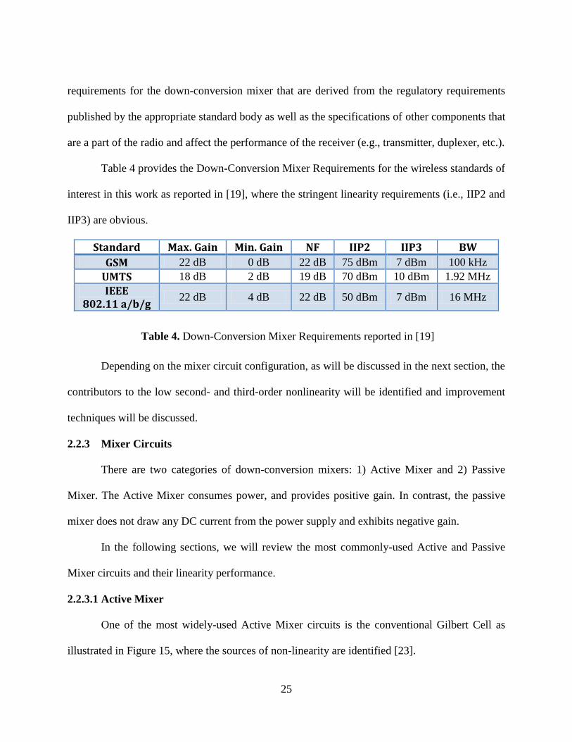
2.2.2 Mixer Requirements................................................................................................ 24
2.2.3 Mixer Circuits ......................................................................................................... 25
3 Available Noise Cancellation Techniques............................................................................. 34
3.1 Introduction .................................................................................................................... 34
3.2 Capacitive Cross-Coupling Noise Cancellation ............................................................. 34
3.3 Cross-Coupling Noise Cancellation Technique ............................................................. 36
4 Proposed LNA Circuit Topology and its Analysis ................................................................ 38
4.1 Proposed Circuit Topology ............................................................................................ 38
4.2 Input Matching and Gain................................................................................................ 40
4.3 Noise Figure ................................................................................................................... 44
4.4 LNA Design Parameters................................................................................................. 49
5 Simulation Results ................................................................................................................. 50
5.1 Gain, Matching, and Isolation ........................................................................................ 50
5.1.1 Conversion Gain ..................................................................................................... 50
5.1.2 Matching ................................................................................................................. 51
5.1.3 Isolation................................................................................................................... 53
5.2 Noise Performance ......................................................................................................... 56
5.2.1 Noise Figure ............................................................................................................ 56
5.2.2 Minimum Noise Figure ........................................................................................... 58
5.3 Stability Analysis ........................................................................................................... 60
5.3.1 Load Stability Circles ............................................................................................. 60
vi
5.3.2 Source Stability Circles........................................................................................... 63
5.4 Linearity Analysis .......................................................................................................... 66
5.4.1 Input-Referred 1dB Compression Point.................................................................. 67
5.4.2 Input-Referred Second-Order Intercept Point (IIP2) .............................................. 69
5.4.3 Input-Referred Third-Order Intercept Point (IIP3) ................................................. 72
5.5 LNA Performance Summary .......................................................................................... 75
5.6 Performance Comparison ............................................................................................... 76
6 Conclusion and Future Work................................................................................................. 78
6.1 Conclusion ...................................................................................................................... 78
6.2 Future Work ................................................................................................................... 78
References ..................................................................................................................................... 80

vii
List of Tables
Table 1. Frequency Bands of DCS1800, PCS1900, AWS1700, and IMT2100 ............................. 8
Table 2. GSM Signal Characteristics and Receiver Specifications [20] ........................................ 8
Table 3. UMTS Signal Characteristics and Receiver Specifications [20] ...................................... 9
Table 4. Down-Conversion Mixer Requirements reported in [19] ............................................... 25
Table 5. Optimum Device Parameters obtained from simulation................................................. 49
Table 6. Performance Characteristics of the Proposed LNA ........................................................ 76
Table 7. Comparison of the Performance Characteristics with [5] ............................................... 76

viii
List of Figures
Figure 1. Global Multi-Standard Frequency Spectrum................................................................... 2
Figure 2. Multi-Standard Frontend using Multiple Narrowband Receivers ................................... 4
Figure 3. Multi-Standard Frontend using Wideband Receiver Frontend ....................................... 5
Figure 4. Reconfigurable Receiver Frontend .................................................................................. 7
Figure 5. Concurrent dual-band LNA proposed in [7] ................................................................. 10
Figure 6. Inductively-Degenerated Tuned Common-Source Amplifier ....................................... 11
Figure 7. Multi-Standard Inductively-Degenerated LNA ............................................................. 13
Figure 8. Tuned Common-Gate Amplifier ................................................................................... 14
Figure 9. Negative Voltage-Voltage Feedback Topology as proposed in [13] ............................ 16
Figure 10. Differential Implementation of the Negative Feedback LNA in [13] ......................... 17
Figure 11. Positive Voltage-Current Feedback Topology as proposed in [5] .............................. 19
Figure 12. Complete Differential LNA as proposed in [5]. .......................................................... 20
Figure 13. Superheterodyne Receiver Architecture ...................................................................... 22
Figure 14. Direct Down-Conversion (Zero IF) Receiver Architecture......................................... 23
Figure 15. Gilbert Cell [23] .......................................................................................................... 26
Figure 16. Switching Pair equivalent model for 2nd
-order IM Distortion analysis ....................... 27
Figure 17. Pseudo-Differential Transconductor to improve linearity [23] ................................... 28
Figure 18. Mitigation of Switching Pair non-linearity [23] .......................................................... 29
Figure 19. Generic Configuration of Passive Mixer from [24] .................................................... 30
Figure 20. Passive Mixer loaded with Common-Gate Buffer [24] ............................................... 31
Figure 21. Passive Mixer loaded with OpAmp-based Current Buffer [24] .................................. 32

ix
Figure 22. LNA as Transconductor in Passive Mixer [24] ........................................................... 32
Figure 23. Capacitive Cross-Coupling Technique in [16] ............................................................ 34
Figure 24. LNA with Capacitive Cross-Coupling in [16]............................................................. 35
Figure 25. Cross-Coupling Noise Cancellation Technique as employed in [6] ........................... 36
Figure 26. Proposed Multiband LNA Architecture ...................................................................... 39
Figure 27. Half-Circuit Topology for the Proposed Multiband LNA ........................................... 41
Figure 28. Proposed LNA core for Noise Calculation .................................................................. 45
Figure 29. Conversion Gain of the proposed LNA ....................................................................... 50
Figure 30. Conversion Gain of the proposed LNA (Close up view) ............................................ 51
Figure 31. Input Return Loss, , of the proposed LNA ........................................................... 52
Figure 32. Input Return Loss, , of the proposed LNA (Close up view)................................. 53
Figure 33. Output-to-Input Isolation, , of the proposed LNA ................................................ 54
Figure 34. Output-to-Input Isolation, , of the proposed LNA (Close up view) ..................... 55
Figure 35. Noise Figure curves of the proposed LNA .................................................................. 57
Figure 36. Noise Figure curves of the proposed LNA (Close up view) ....................................... 58
Figure 37. Minimum Noise Figure curves of the proposed LNA ................................................. 59
Figure 38. Minimum Noise Figure curves of the proposed LNA (Close up view) ...................... 59
Figure 39. Load Stability circles of the proposed LNA for the DCS1800 band. .......................... 61
Figure 40. Load Stability circles of the proposed LNA for the PCS1900 band ........................... 62
Figure 41. Load Stability circles of the proposed LNA for the IMT2100 band ........................... 63
Figure 42. Source Stability circles of the proposed LNA for the DCS1800 band ........................ 64
Figure 43. Source Stability circles of the proposed LNA for the PCS1900 band ........................ 65
Figure 44. Source Stability circles of the proposed LNA for the IMT2100 band ........................ 66
x
Figure 45. Input-Referred 1dB Compression Point for the DCS1800 band ................................. 67
Figure 46. Input-Referred 1dB Compression Point for the PCS1900 band .................................. 68
Figure 47. Input-Referred 1dB Compression Point for the IMT2100 band ................................. 69
Figure 48. Input-Referred IP2 of the proposed LNA for the DCS1800 band ............................... 70
Figure 49. Input-Referred IP2 of the proposed LNA for the PCS1900 band ............................... 71
Figure 50. Input-Referred IP2 of the proposed LNA for the IMT2100 band ............................... 72
Figure 51. Input-Referred IP3 of the proposed LNA for the DCS1800 band ............................... 73
Figure 52. Input-Referred IP3 of the proposed LNA for the PCS1900 band ............................... 74
Figure 53. Input-Referred IP3 of the proposed LNA for the IMT2100 band ............................... 75

xi
List of Abbreviations
AC Alternating Current
ADC Analog-to-Digital Converter
AM Amplitude Modulation
ANT. Antenna
AWS Advanced Wireless Services
BiCMOS Bipolar Complementary Metal-Oxide Semiconductor
BPF Band-Pass Filter
CDMA Code-Division Multiple-Access
CMOS Complementary Metal-Oxide Semiconductor
DC Direct Current
DCS Digital Communication System
DVB-H Digital Video Broadcast - Handheld
E-GSM Enhanced Global System for Mobile Communications
GPS Global Positioning System
GSM Global System for Mobile Communications
HBT Heterojunction Bipolar Transistor
IEEE Institute of Electrical and Electronics Engineers
IF Intermediate Frequency
IM2 Second-order Inter-Modulation
IIP2 Input-referred second-order Intercept Point
IIP3 Input-referred third-order Intercept Point

xii
IMT International Mobile Telecommunications
I/Q In-phase/Quadrature-phase
KCL Kirchhoff's Current Law
KVL Kirchhoff's Voltage Law
LAN Local-Area Network
LPF Low-Pass Filter
LNA Low-Noise Amplifier
LO Local Oscillator
MOS Metal-Oxide Semiconductor
NF Noise Figure
OpAmp Operational Amplifier
PAN Private-Area Network
PCS Personal Communication System
PLL Phase-Locked Loop
RF Radio Frequency
SAW Surface Acoustic Wave
SDR Software-Defined Radio
SMD Surface-Mount Device
UMTS Universal Mobile Telephone System
VCO Voltage-Controlled Oscillator
VGA Variable-Gain Amplifier
WCDMA Wideband Code-Division Multiple-Access
WiFi Wireless Fidelity

xiii
WiMax Worldwide Interoperability for Microwave Access
WLAN Wireless Local-Area Network
1
1 Introduction
1.1 Background
The evolution of mobile wireless communication standards over the past three (3)
decades has been unimaginable. Almost every technology that has been introduced continues to
exist and evolve while new standards are being added. These standards, while some were
developed for a specific geographic region, have spread to the rest of the world. For example,
CDMA2000 was developed in the USA; however, it enjoys hundreds of millions of subscribers
across the world [1]. Similarly, GSM was a trans-European standard; nevertheless, it is currently
operational in almost every country in the world [2].
In addition to the multitude of these standards (e.g., Bluetooth, GPS, IEEE 802.11,
WiMax, and DVB-H), a given standard generally operates on different frequency bands
depending on the country or the region. For example, GSM operates in 900MHz and 1800MHz
bands (also known as E-GSM and DCS1800, respectively) in Europe and Asia, while 850MHz
and 1900MHz bands (also known as Cellular and PCS1900, respectively) are primarily used in
North America. Similarly, the UMTS (WCDMA) operates in the 2.1/1.7GHz (Downlink/Uplink)
band (known as AWS1700) in North America while the 2.1/1.9GHz (Downlink/Uplink) band
(known as IMT2100) is utilized in the rest of the world.
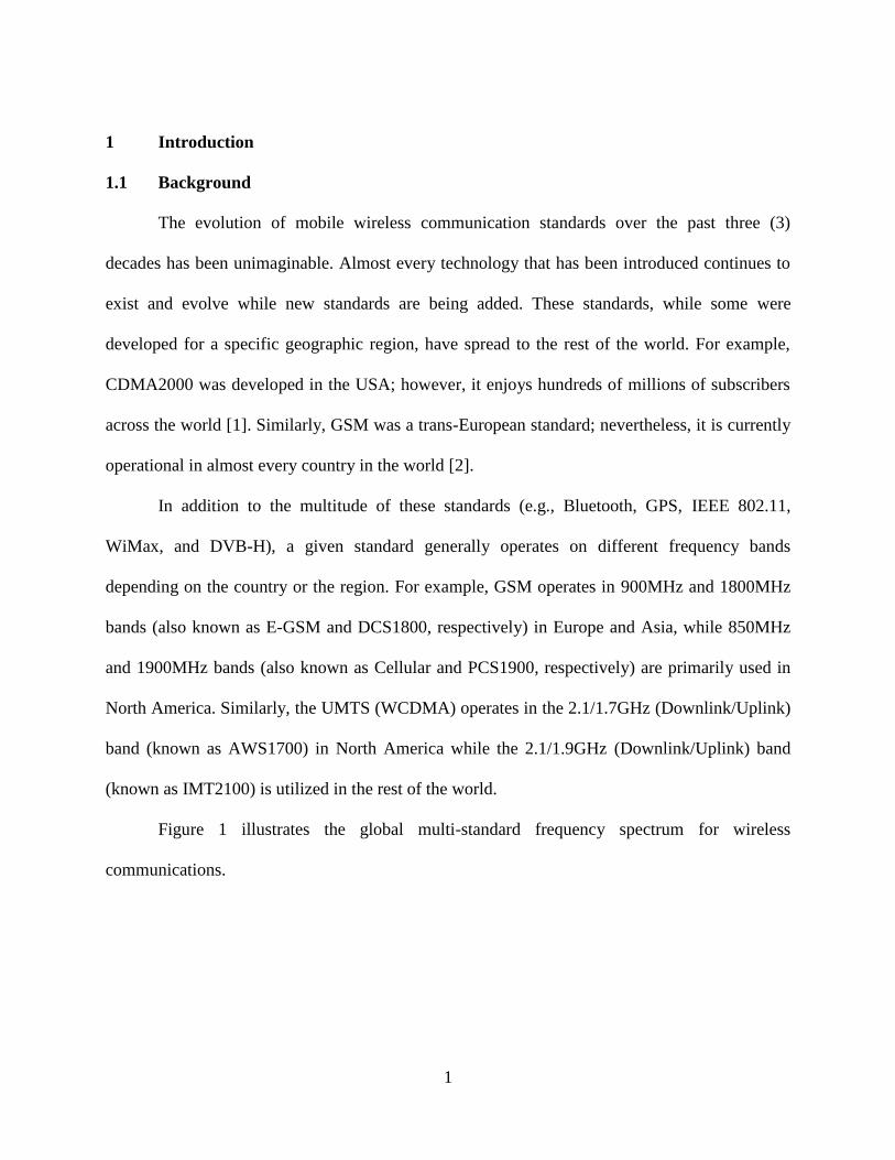
Figure 1 illustrates the global multi-standard frequency spectrum for wireless
communications.

2
0 1 Freq. (GHz)2 3 4 5 6
GS
M / C
DM
A2
00
0
GS
M / C
DM
A2
00
0
UM
TS
GP
S
DV
B-H
DV
B-H
Blu
eto
oth
/ IE
EE
80
2.1
1b
/g/n
WiM
ax
IEE
E8
02.1
1a
Figure 1. Global Multi-Standard Frequency Spectrum
This amalgamate of standards and their associated frequency spectrums have created an
ongoing and increasingly challenging situation for mobile handset manufacturers, as they have to
incorporate as many of these standards in their product as possible due to consumer and network
operators’ demands; the latter arising from the need for seamless and interoperable
communication for users in this increasingly mobile world.
Given that the current trend in manufacturing multi-standard mobile handsets does not
scale due to utilizing a dedicated chipset for each standard, a new design approach is required
that incorporates all wireless standards and frequency bands with maximum sharing of the
hardware among the standards in order to minimize the circuit area and power consumption and
be feasible for production, hence the need for multi-standard and reconfigurable radio; also
known as Software-Defined Radio (SDR).
The design of the receiver and the transmitter of the SDR is very challenging and is
currently the subject of on-going research. As such, in this work, we will solely focus on the
Receiver Frontend.
1.2 Current Receiver Frontend Design Architectures

3
Currently, there are two (2) major approaches in the design of the Multi-Standard
Receiver Frontend: 1) Narrowband Frontend, which is the conventional method of handling
multiple frequency bands or standards, and 2) Wideband Frontend, which has become of great
interest recently, and several publications have been released to address the challenges associated
with the topology.
We will first discuss these two architectures in detail and then present the Reconfigurable
Receiver Frontend architecture as a practical approach between the above-mentioned two (2)
extremes of the Frontend topology.
1.2.1 Narrowband Receiver Frontend Architecture
Figure 2 illustrates the spectrum selection and circuit architecture for the Multi-Standard
Receiver utilizing Narrowband Frontend topology.
0 1 Freq. (GHz)2 3 4 5 6

4
LPF 1
LO 1
Narrowband
RF LNA 1
Single-Band
ANT. (f1) Mixer
VGA 1
ADC 1
Digital Domain
Signal 1
LPF n
LO n
Narrowband
RF LNA n
Single-Band
ANT. (fn) Mixer
VGA n
ADC n
Digital Domain
Signal n
Figure 2. Multi-Standard Frontend using Multiple Narrowband Receivers
As is evident, this type of receiver selects the desired frequency band only [4].
Furthermore, for each frequency band or standard, a dedicated frontend path is utilized. As such,
the topology occupies significant silicon die area and is not scalable as more standards are
introduced. The Narrowband Receiver Frontend provides frequency selectivity and is immune to
out-of-band interference; therefore, it has superior linearity. Furthermore, due to narrow-band
input matching requirement, excellent return loss and noise figure may be achieved. Ultimately,
this approach consumes less power, as each receiver path is optimized to operate for a specific
band.
1.2.2 Wideband Receiver Frontend Architecture

5
Figure 3 illustrates the spectrum selection and circuit architecture for the Wideband
Receiver Frontend, where all wireless standards are simultaneously received and the baseband
circuitry selects the desired signal [3], [11], and [12].
0 1 Freq. (GHz)2 3 4 5 6
Figure 3. Multi-Standard Frontend using Wideband Receiver Frontend
While the Wideband Receiver Frontend allows concurrent reception of more than one
standard, it is not an optimum approach to meet the regulatory requirements of each standard.
Furthermore, due to the very wide band of operation, the odd- and even-order inter-modulation
products of the desired frequency may fall on other desired frequencies. For example, the third-
order inter-modulation products generated by strong DCS1800 or PCS1900 signals may fall on
top of the 5GHz WLAN signal [19]. In order to sustain operation in the presence of such
blockers, the wideband receiver frontend must have extremely high linearity. The following
example from [19] demonstrates the severity of this issue with practical data:
In order to demodulate a 16MHz WLAN signal with a 9dB NF receiver, the input-
referred noise floor at 5GHz can be calculated as:

6
Assuming 0dBm power for the DCS or PCS blocker signal and in order for the third-
order inter-modulation product to be below the noise floor, the wideband receiver IIP3 may be
calculated as follows:
Obviously, achieving such a high IIP3 is not practical in Integrated Circuits. This simple
example demonstrates how critical the issue of out-of-band blockers and consequently high
linearity requirement is for the wideband receiver frontend.
Despite the above discouraging statements, the wideband receiver frontend is one of the
dominant architectures for the realization of Software-Defined Radio Receiver.
1.3 Reconfigurable Receiver Frontend
The foregoing sections provided the necessary background information for the
introduction of Reconfigurable Receiver Frontend. The reader might have concluded by now that
the optimum architecture for a multi-standard receiver is neither a wideband nor a narrowband
receiver. Indeed, it is an architecture that handles multiple standards while rendering the highest
level of integration and hardware sharing and is scalable. We call this architecture a
Reconfigurable Receiver Frontend.
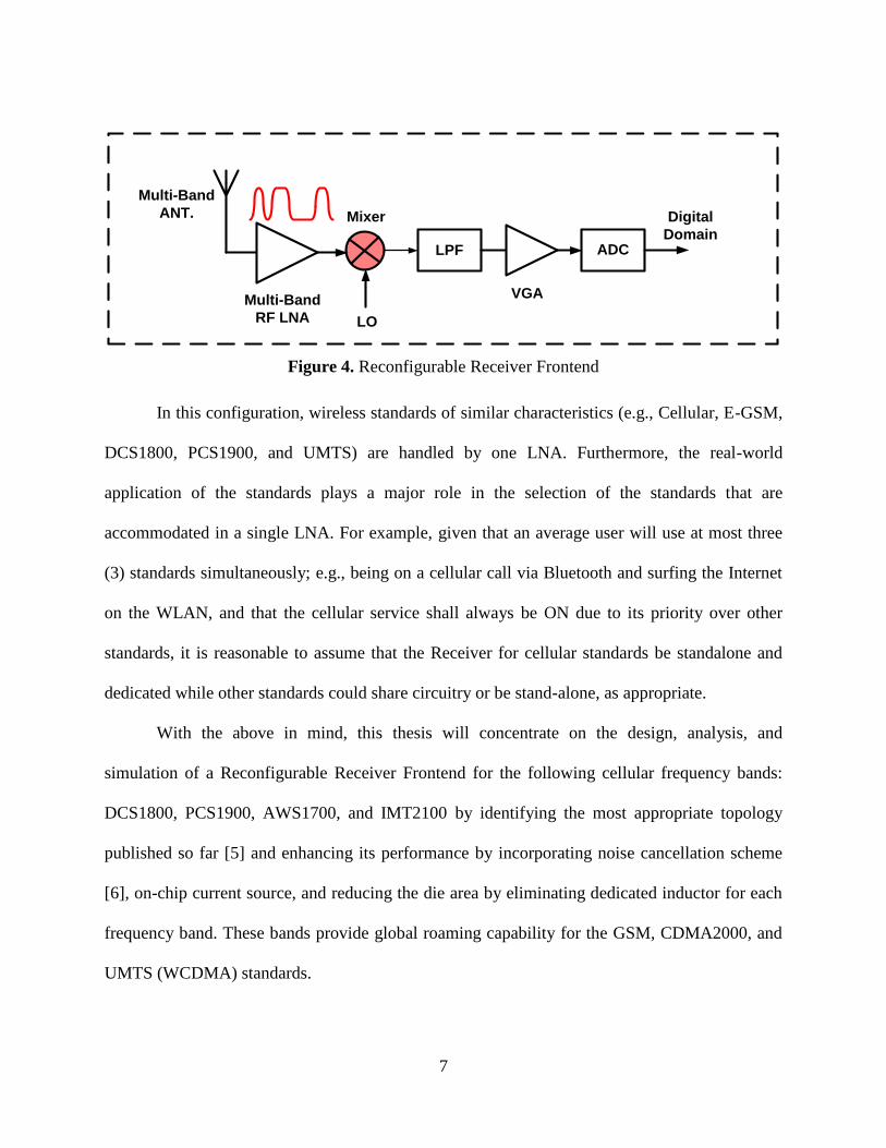
Figure 4 illustrates the multi-standard Reconfigurable Receiver Frontend utilizing a
single LNA for all homogenous standards.
7
LPF
LO
Multi-Band
RF LNA
Multi-Band
ANT. Mixer
VGA
ADC
Digital
Domain
Figure 4. Reconfigurable Receiver Frontend
In this configuration, wireless standards of similar characteristics (e.g., Cellular, E-GSM,
DCS1800, PCS1900, and UMTS) are handled by one LNA. Furthermore, the real-world
application of the standards plays a major role in the selection of the standards that are
accommodated in a single LNA. For example, given that an average user will use at most three
(3) standards simultaneously; e.g., being on a cellular call via Bluetooth and surfing the Internet
on the WLAN, and that the cellular service shall always be ON due to its priority over other
standards, it is reasonable to assume that the Receiver for cellular standards be standalone and
dedicated while other standards could share circuitry or be stand-alone, as appropriate.
With the above in mind, this thesis will concentrate on the design, analysis, and
simulation of a Reconfigurable Receiver Frontend for the following cellular frequency bands:
DCS1800, PCS1900, AWS1700, and IMT2100 by identifying the most appropriate topology
published so far [5] and enhancing its performance by incorporating noise cancellation scheme
[6], on-chip current source, and reducing the die area by eliminating dedicated inductor for each
frequency band. These bands provide global roaming capability for the GSM, CDMA2000, and
UMTS (WCDMA) standards.

8
Table 1 provides information on the spectrum of the above-referenced four (4) cellular
Frequency Bands.
Frequency Band Downlink Uplink
DCS1800 1805-1880 MHz 1710-1785 MHz
PCS1900 1930-1990 MHz 1850-1910 MHz
AWS1700 2110-2155 MHz 1710-1755 MHz
IMT2100 2110-2170 MHz 1920-1980 MHz
Table 1. Frequency Bands of DCS1800, PCS1900, AWS1700, and IMT2100
As is obvious from this table, the AWS1700 downlink spectrum is confined within that of
IMT2100; as such, no additional circuit component is required to accommodate this service;
however, for the transmitter, the design will be different, and may require separate circuitry
depending on the topology adopted. Furthermore, when referring to IMT2100 in the rest of this
document, AWS1700 is also implied.
1.4 Signal Characteristics and Receiver Requirements
Table 2 provides the GSM Signal Characteristics and the E-GSM, DCS1800, and
PCS1900 Receiver Specifications as reported in [20]. It shall be noted that these specifications
apply to the entire Receiver Frontend (i.e., the LNA and the Mixer combined).
E-GSM/DCS/PCS Requirement
Channel Bandwidth 200 kHz
Noise Figure 9 dB
IIP3 -18 dBm
IIP2 +49 dBm
Table 2. GSM Signal Characteristics and Receiver Specifications [20]
The stringent second-order Input Intercept Point, IIP2, requirement stems from the AM
suppression test as detailed in [21].

9
Similarly, Table 3 provides the UMTS (WCDMA) Signal Characteristics and the
Receiver Specifications as reported in [20] that apply to the entire Receiver Frontend (i.e., the
LNA and the Mixer combined).
UMTS Requirement
Channel Bandwidth 5 MHz
Noise Figure 9 dB
IIP3 -17 dBm
IIP2 +46 dBm
Table 3. UMTS Signal Characteristics and Receiver Specifications [20]
1.5 Organization of the Thesis
The organization of this document is as follows: Section 2 will review the available
circuit topologies for Reconfigurable Receiver Frontends, and compare their strengths and
weaknesses, and, ultimately, identify the most suitable configuration for the implementation of a
practical multi-standard Receiver Frontend.
In Section 3, the existing noise cancellation techniques will be reviewed and the most
appropriate circuitry will be identified for incorporation in the proposed Reconfigurable Receiver
Frontend architecture.
Section 4 will present the proposed Reconfigurable Receiver Frontend architecture;
utilizing the outcome of the evaluations conducted in Sections 2 and 3. Furthermore, the
mathematical analysis of the proposed topology will be presented for Gain, Input Matching, and
Noise performance.
The simulation results for the proposed Reconfigurable Receiver Frontend will be
presented in Section 5. In addition, they will be compared with the closest topology published so
far.
Finally, Section 6 will conclude the document and summarize the future work.

10
2 Available Topologies for Reconfigurable Receiver Frontends
2.1 Low-Noise Amplifier (LNA) Topologies
As the name implies, the Reconfigurable Receiver Frontend is expected to select and
amplify a few bands either concurrently [7] (Figure 5) or one-at-a-time.
Vin
Lg
Cg
Lg2
Cgs
Ls
Vbias
L1
C1
L2C2
Vdd
Vout
Dual-
Resonance
Output
Network
Dual-
Resonance
Input
Matching
Network
Figure 5. Concurrent dual-band LNA proposed in [7]
The LNA in Figure 5 supports concurrent amplification of the 2.5GHz and 5GHz
frequency bands, and the signals may be separated in the baseband for simultaneous processing,
depending on the mixer topology adopted [19]. For the low-band operation, (SMD),
(Bond-wire), and constitute the input matching network, while for the high-band, the SMD
capacitor ( ) bypasses . At the output, a dual-resonant tank topology is leveraged to provide
frequency selectivity and gain for the given band [19].
11
Considering the fact that, in practice, only one of the frequency bands listed in Table 1
will be active and operational at any given time, concurrent reception and amplification of the
frequency bands is neither required nor desired.
For an amplifier to select and amplify a given band, depending on its topology, either
both the input and the output terminals (e.g., in Common-Source configuration), or at least the
output terminal (i.e., in Common-Gate topology), must be tuned to that band.
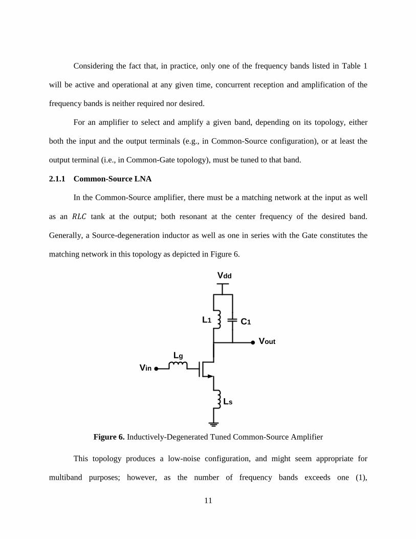
2.1.1 Common-Source LNA
In the Common-Source amplifier, there must be a matching network at the input as well
as an tank at the output; both resonant at the center frequency of the desired band.
Generally, a Source-degeneration inductor as well as one in series with the Gate constitutes the
matching network in this topology as depicted in Figure 6.
Vin
Lg
Ls
L1 C1
Vdd
Vout
Figure 6. Inductively-Degenerated Tuned Common-Source Amplifier
This topology produces a low-noise configuration, and might seem appropriate for
multiband purposes; however, as the number of frequency bands exceeds one (1),

12
implementation of an input matching network capable of passing multiple bands becomes
difficult, if not impractical, as it is narrow-band and not capable of supporting multiband
requirements [8]. Furthermore, the frequency alignment of the input matching network and the
load tank becomes a major issue due to the variation of the values of and caused by the
fabrication process. In addition, for every additional band, an inductor must be added to the input
matching network, which increases the circuit die area significantly. Finally, using low-Q input
matching network to create wideband input will result in increased noise figure of the amplifier.
As such, the Common-Source amplifier configuration is not suitable for multiband amplification
purposes.
Nevertheless, a wideband version of this amplifier was presented in [22] and illustrated in
Figure 7 below.

13
GSM900 IN DCS1800 IN PCS1900 IN WCDMA IN
BiasBiasOUT1 OUT2
GSM900
DCS1800
PCS1900
WCDMA
Figure 7. Multi-Standard Inductively-Degenerated LNA
This configuration supports the main cellular standards and frequency bands; i.e.,
GSM900, DCS1800, PCS1900, and UMTS bands via four (4) dedicated input ports for each
spectrum segment. Furthermore, the output is split into two (2) tuned loads to resonate at the
low-band GMS900 as well as the high-band DCS/PCS/UMTS. The topology proves to render
high performance; however, due to utilization of several inductors (both off-chip and integrated),
the configuration is less than desirable to be considered as a scalable candidate for
Reconfigurable Receiver Frontend [19].
2.1.2 Common-Gate LNA

14
In contrast to the inductively-degenerated Common-Source Amplifier, the Common-Gate
topology does not require an input matching network (as depicted in Figure 8) due to its
wideband input characteristics (limited by input pad capacitance and bond-wire inductance).
Nevertheless, input matching is achieved by adjusting the bias current (i.e., ) appropriately in
order to satisfy the following equation:
. Furthermore, as will be discussed in Section
2.1.3 and confirmed mathematically in Section 4, employing a feedback network around the
Common-Gate amplifier will, in fact, make its input impedance a function of the load
impedance; as such, by switching one reactive element in the load tank; i.e., modifying the load
tank resonance frequency, the input is also tuned to the desired band without the need for any
extra passive component for input matching [13], [14].
Vbias
Ls
L1 C1
Vdd
Vout
Vin
Figure 8. Tuned Common-Gate Amplifier
Before proceeding to the next section, it is worth mentioning that since the frequency
bands listed in Table 1 are between 45 MHz and 75 MHz wide, and that these frequency bands

15
are closely spaced, the tuned amplifier configuration is the most appropriate for the purpose of a
implementing a Reconfigurable Receiver Frontend.
2.1.3 Feedback Amplifiers
So far, we have justified the use of the Common-Gate Amplifier as the most appropriate
candidate for multiband applications. Furthermore, we have eluded that a feedback network
around this configuration results in the input impedance and voltage gain becoming a function of
the load; tuning the input impedance and gain frequency responses by switching a single reactive
element in the load. Another major characteristic of the feedback network is the enhancement of
the linearity; this is due to the high cut-off frequency, , of the sub-micron transistors that
makes feedback-based amplifiers a reality for Radio Frequencies. It shall be noted here that the
feedback network also improves the noise performance of the amplifier under matching
condition [15].
In this section, we will review a few attractive feedback topologies, and adopt the most
suitable configuration for our Reconfigurable Receiver Frontend.
2.1.3.1 Negative Voltage-Voltage Feedback LNA
The half-circuit representation of the Negative Voltage-Voltage Feedback LNA proposed
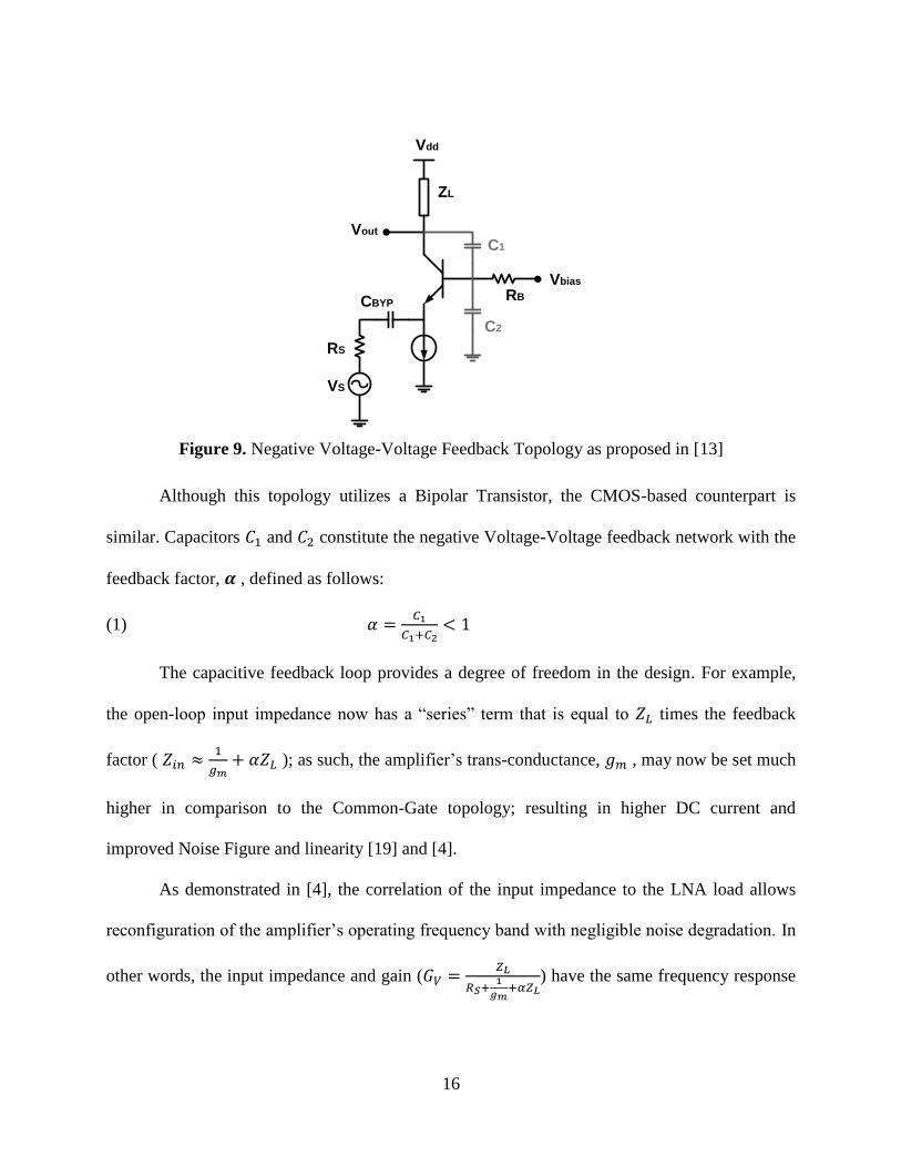
by [13] is depicted in Figure 9.
16
Vbias
RB
Vdd
Vout
C1
C2
CBYP
RS
VS
ZL
Figure 9. Negative Voltage-Voltage Feedback Topology as proposed in [13]
Although this topology utilizes a Bipolar Transistor, the CMOS-based counterpart is
similar. Capacitors and constitute the negative Voltage-Voltage feedback network with the
feedback factor, , defined as follows:
(1)
The capacitive feedback loop provides a degree of freedom in the design. For example,
the open-loop input impedance now has a ―series‖ term that is equal to times the feedback
factor (
); as such, the amplifier’s trans-conductance, , may now be set much
higher in comparison to the Common-Gate topology; resulting in higher DC current and
improved Noise Figure and linearity [19] and [4].
As demonstrated in [4], the correlation of the input impedance to the LNA load allows
reconfiguration of the amplifier’s operating frequency band with negligible noise degradation. In
other words, the input impedance and gain (
) have the same frequency response

17
as the load impedance, . That is, tuning results in the alignment of both the gain and
the input impedance with the desired frequency band [19].
The differential implementation of this LNA, including the tunable load, is depicted in
Figure 10.
Vbias
Vdd
OUT
C1
C2
LSMD
CC
VC
CB
VB
CA
VA
+ -
C2
C1
Vbias
CC
VC
CB
VB
CA
VA
Lload
LSMD
IN+ -
ON Chip
Capacitive
FeedbackCapacitive
Feedback
Figure 10. Differential Implementation of the Negative Feedback LNA in [13]
Capacitors , , and , together with the corresponding MOS switches, allow the
tuning of the LNA to the desired band. One of the advantages of this topology, as it relates to the
load, is that it utilizes a differential inductor, , that minimizes the die area and is shared
among all frequency bands.
Although this topology is appealing; it suffers from major disadvantages as follows:

18
1) It utilizes off-chip inductors, , as the current source. Depending on the frequency
band of operation, the off-chip inductor must be large in order not to load the source.
Furthermore, it may not be a practical approach at lower frequencies. It is worth mentioning that
this specific configuration was implemented for the HiperLAN2/IEEE802.11a frequency bands
that operate in the 5GHz range, where an off-chip inductor of 15 nH will produce adequate
impedance; however, at our lowest frequency of operation; i.e., DCS1800, larger off-chip
inductors are required.
2) Due to the passive nature, and, consequently, less-than-unity feedback factor, the
overall gain of the amplifier is degraded. The unity current gain and large parasitic capacitance at
the output terminal also contributes to lower gain, as the latter reduces the load impedance at
Radio Frequencies.
3) When implemented in pure CMOS, compared to the BiCMOS implementation as
performed in [4], the limitations mentioned in 2) become more pronounced, as the amplifier
transistor must be large to produce adequate ; resulting in additional parasitic capacitance
seen by the load.
4) The use of capacitors in parallel with for every desired band shall be carried out
with caution, as for lower frequencies, larger capacitors will be required, which will degrade the
gain as well as the selectivity of the tank. Since the circuit in [13] was designed for 5 GHz range,
the tank capacitors were less than 200 fF, and this issue was not pronounced; however, in the
case of the frequency bands of interest in this work, a different approach shall be taken to keep
these capacitors as small as possible. One approach is to choose as large an inductor as possible
to resonate with the transistors’ parasitic capacitors at the highest frequency of interest, and

19
utilize capacitors to resonate with the inductor at the remaining frequency bands. We will
employ this latter approach in the architecture of our proposed Multiband LNA
Considering the above disadvantages, this topology does not appear as an appealing
candidate for our reconfigurable LNA; nevertheless, its load configuration; i.e., a differential
inductor in parallel with switched capacitors is worth considering in the design of a multiband
LNA.
2.1.3.2 Positive Voltage-Current Feedback LNA
It was clear from the review of the feedback topology discussed in section 2.1.3.1 that a
negative feedback network must be replaced with one that is both non-capacitive (and non-
passive, in general) and positive in order to produce a larger-than-unity current gain to overcome
the disadvantages mentioned therein.
The half-circuit representation of a Positive Feedback LNA as proposed by [5] is
depicted in Figure 11.
M1
IbiasVS
RS
Zload
-1
Vbias
Vin
Zin
Iin
Iout
M2
Iloop
Loop
Figure 11. Positive Voltage-Current Feedback Topology as proposed in [5]

20
In this topology, represents the tuned tank impedance; while the amplifier with
gain of minus 1 (-1) together with provide the positive current feedback. The gain of minus 1
is achieved by crossing the drains of the amplifier transistors in the differential configuration as
depicted in Figure 12. Furthermore, the feedback factor, , input impedance, and gain are
derived as follows:
(2)
(3)
(4)
Tunable Load
Vbias
Variable
Gain
V3 M5M1
Off-Chip
Vin+ -
M3M6
V3
Variable
Gain
Vbias
M4 M2
V2
L1 L3
V1L2 diff L4 diff
+ -Vout
VDD
Figure 12. Complete Differential LNA as proposed in [5].
Although this topology addresses some of the major disadvantages of the configuration of
Figure 10, it still suffers from the following:

21
1) The LNA utilizes off-chip inductors as current source, which, similar to the topology
depicted in Figure 10, is undesirable, and an approach must be adopted to eliminate it.
2) Given that it is implemented in pure CMOS technology, it has high noise figure
compared to that proposed in [13], which utilizes intrinsically-low-noise HBTs. However, it
lacks any noise cancellation scheme as evident from the high noise figure reported and provided
in Table 7 for comparison.
3) The load tank utilizes so many inductors, which contribute to large die area. The
authors of [5] claim that an inductor-only-based load tank provides higher quality factor;
however, given the narrow bandwidth of the frequency spectrums of interest in this work, low-
value capacitors may be utilized in parallel to a differential inductor, as employed in [13], to
provide high-quality-factor load tank.
As will be demonstrated in 4, the advantage of the Positive Feedback LNA is to provide
higher than unity current gain; increasing the Transconductance Gain of the amplifier and
providing a degree of freedom for input matching.
As such, if the disadvantages mentioned above are addressed and eliminated, this
topology may be an acceptable candidate for a reconfigurable LNA.
2.2 Down-Conversion Mixers
2.2.1 Receiver Architectures
Prior to directing our attention to the available down-conversion mixer circuit topologies
appropriate for Reconfigurable Receiver Frontend, we shall review the common Receiver
Architectures, as they will provide insight into both the suitable receiver architecture for multi-
standard applications and the role of down-conversion mixers in the overall receiver
configuration.

22
There are three (3) major classes of Receiver Architectures [25]: 1) Superheterodyne
Receiver. 2) Direct Down-Conversion Receiver (also known as Zero IF Receiver), and 3) Low IF
Receiver. The following sections will provide a high-level review of these topologies and
identify the optimum configuration for reconfigurable receiver frontend.
2.2.1.1 Superheterodyne Receiver
Figure 13 illustrates the Superheterodyne Receiver Architecture [25], where the RF signal
received by the antenna is down-converted to baseband using two down-conversion mixers.
90°
ADC
BPF
LNA
LO1
BPF
VGA
ADC
LPF
LPF
I
Q
LO2
Analog Domain Digital Domain
Figure 13. Superheterodyne Receiver Architecture
The first down-conversion occurs from RF to IF; as such, the use of image rejection
band-pass filter before the first mixer is necessary. Further, the signal, after filtering and
amplification stages, is down-converted from IF to baseband in order to be made available for
the ADC and the subsequent digital processing step.
Although the Superheterodyne architecture possesses such advantages as high
performance, low power, no DC offset, low design risk, easier design of the LNA and mixer, it
suffers from the following disadvantages that render it unsuitable for reconfigurable multi-
standard receiver frontend purposes: high cost, the need for two (i.e., for IF and RF) synthesizers,

23
two mixers, two filters, and external components such as SAW filter. As such, this configuration
is not scalable and suffers from poor and low integration.
2.2.1.2 Direct Down-Conversion (Zero IF) Receiver
Figure 14 illustrates the Direct Down-Conversion (Zero IF) Receiver architecture [25],
where the RF signal is directly down-converted to baseband (around DC), hence the name Direct
Down-Conversion.
90°
ADC
BPF
LNA
ADC
LPF
LPF
I
Q
LO1
Analog Domain Digital Domain
VGA
VGA
Figure 14. Direct Down-Conversion (Zero IF) Receiver Architecture
The Zero IF receiver architecture benefits from reduced number of components compared
to Superheterodyne configuration. This is due to the elimination of the IF SAW filter, the IF
PLL, and the image rejection filter. This results in a low-cost receiver topology that enjoys high
level of integration. As such, the Zero IF receiver architecture is ideal for reconfigurable receiver
frontend purposes.
Nevertheless, the Zero IF configuration suffers from the following disadvantages: On-
board Power Amplifier inject locking the VCO, Difficulty in achieving good I/Q quadrature

24
balance at RF frequencies, LO self-mixing that causes DC offset, AM detection that requires
large second-order linearity (IIP2), and flicker noise of the mixer.
It shall be stated that the advantages of the Zero IF architecture overweigh its
disadvantages, and has made this topology a widely-used configuration for radio receivers [25].
Also, some of the disadvantages such as DC offset or flicker noise are not so critical for
wideband signals; e.g., UMTS (1.92MHz at baseband) or IEEE802.11 (16MHz at baseband).
2.2.1.3 Low IF Receiver
Similar to the Zero IF receiver, the RF signal is down-converted in one stage; however, in
order to avoid the DC offset and flicker noise issues, the signal is down-converted to a higher
frequency than DC, hence the name Low IF.
The Low IF and Zero IF receiver architectures are identical as far as the analog domain is
concerned, except for the bandwidth (cut-off frequency) of the Low-Pass Filter and the
performance of the ADC. In the Low IF configuration, the LPF bandwidth is much higher than
the signal bandwidth. As such, the ADC must be high-performance and robust in order to
digitize a wider band and extract the desired channel.
Clearly, the Low IF topology possesses the same advantages as the Zero IF configuration.
However, it is an inevitable architecture for narrow-band signals such as GSM (100 kHz at
baseband). Nevertheless, since the analog elements of the Zero- and Low-IF receivers are
identical, in the rest of this document, when we refer to Zero IF receiver, the Low IF receiver is
also implied if the signal bandwidth is narrow.
2.2.2 Mixer Requirements
Before we proceed to the discussion of the available mixer circuit architectures and their
suitability for the Reconfigurable Receiver Frontend, it is prudent to review the circuit-level
25
requirements for the down-conversion mixer that are derived from the regulatory requirements
published by the appropriate standard body as well as the specifications of other components that
are a part of the radio and affect the performance of the receiver (e.g., transmitter, duplexer, etc.).
Table 4 provides the Down-Conversion Mixer Requirements for the wireless standards of
interest in this work as reported in [19], where the stringent linearity requirements (i.e., IIP2 and
IIP3) are obvious.
Standard Max. Gain Min. Gain NF IIP2 IIP3 BW
GSM 22 dB 0 dB 22 dB 75 dBm 7 dBm 100 kHz
UMTS 18 dB 2 dB 19 dB 70 dBm 10 dBm 1.92 MHz
IEEE 802.11 a/b/g
22 dB 4 dB 22 dB 50 dBm 7 dBm 16 MHz
Table 4. Down-Conversion Mixer Requirements reported in [19]
Depending on the mixer circuit configuration, as will be discussed in the next section, the
contributors to the low second- and third-order nonlinearity will be identified and improvement
techniques will be discussed.
2.2.3 Mixer Circuits
There are two categories of down-conversion mixers: 1) Active Mixer and 2) Passive
Mixer. The Active Mixer consumes power, and provides positive gain. In contrast, the passive
mixer does not draw any DC current from the power supply and exhibits negative gain.
In the following sections, we will review the most commonly-used Active and Passive
Mixer circuits and their linearity performance.
2.2.3.1 Active Mixer
One of the most widely-used Active Mixer circuits is the conventional Gilbert Cell as
illustrated in Figure 15, where the sources of non-linearity are identified [23].

26
RF+ RF-
Y
LO+
LO-
LO+
VOUT+ VOUT-
2nd
Order Distortion
Self-mixing, 2nd
Order Distortion
Common-mode to
differential conversion
Figure 15. Gilbert Cell [23]
Although the conventional Gilbert cell mixer exhibits IIP2 figure of near +90 dBm at
frequencies up to tens of MHz, the IIP2 swiftly declines at GHz frequencies [23]. This is
primarily due to the second-order Inter-Modulation distortion contributed by the following
phenomena [26]: 1) Self Mixing, 2) Mismatch in Load Resistors, 3) Transconductor nonlinearity,
and 4) Switching Pair nonlinearity
The self-mixing occurs as a result of the LO signal being coupled to the RF input and
appearing at the source of the Switching Pair and consequently mixing with the LO. Fortunately,
layout counter-measures may be utilized to alleviate this issue [23]. For example, by spacing the
RF and LO metal tracks as far as possible or, if intersection is unavoidable, crossing them over
orthogonally to minimize coupling.
27
The mismatch in load resistors will result in the conversion of the second-order common-
mode components into differential [23]. Fortunately, utilizing highly linear poly-silicon load
resistors is a remedy that will maintain the mismatch below 0.1% [23].
It was demonstrated in [26] that the fully differential transconductor configuration
provides the highest third-order linearity (i.e., IIP3). As will be seen shortly, other considerations
lead to the adoption of a pseudo-differential topology.
The foregoing remedies for second-order IM distortion leave the Switching Pair non-
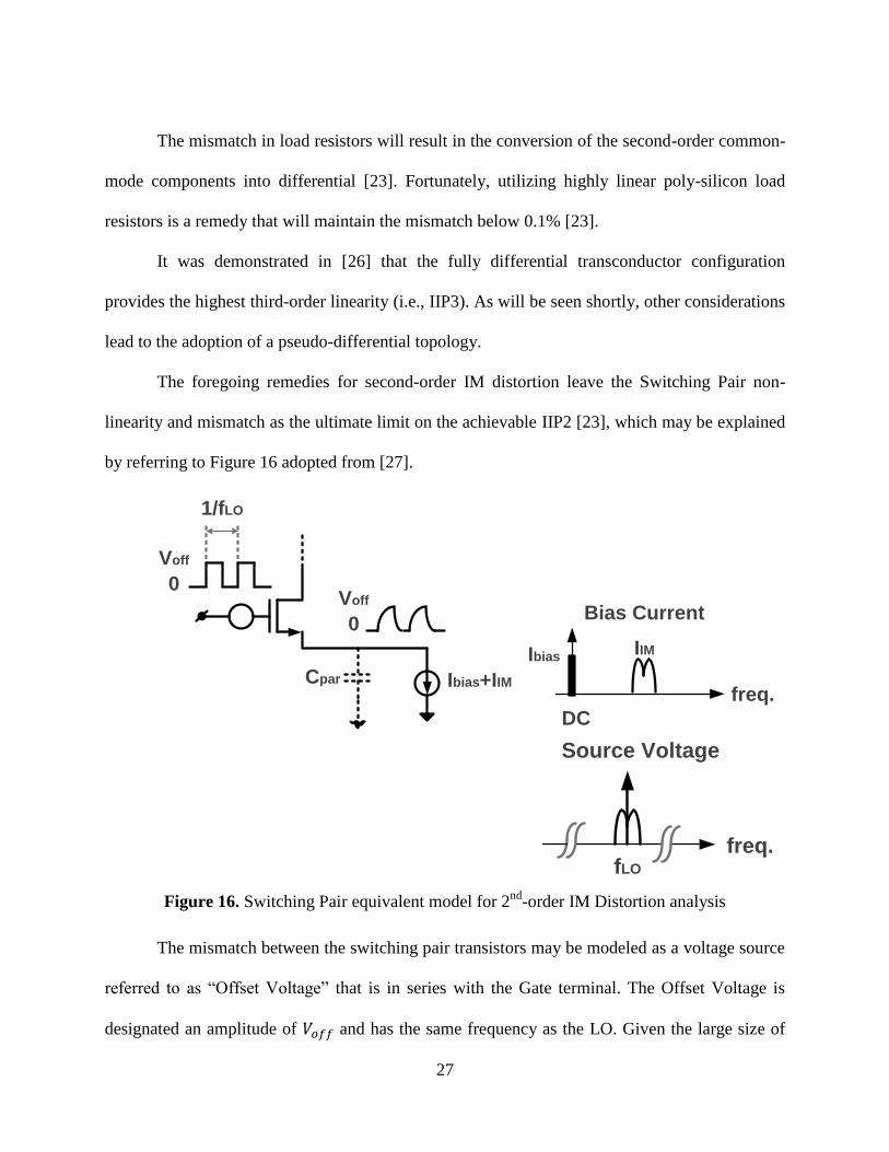
linearity and mismatch as the ultimate limit on the achievable IIP2 [23], which may be explained
by referring to Figure 16 adopted from [27].
Cpar
1/fLO
0
Voff
0
Voff
Ibias+IIMfreq.
DC
Ibias
Bias Current
IIM
freq.
Source Voltage
fLO
Figure 16. Switching Pair equivalent model for 2nd
-order IM Distortion analysis
The mismatch between the switching pair transistors may be modeled as a voltage source
referred to as ―Offset Voltage‖ that is in series with the Gate terminal. The Offset Voltage is
designated an amplitude of and has the same frequency as the LO. Given the large size of

28
the switching pair transistors to mitigate the flicker noise, the parasitic capacitance seen at the
Source terminals (i.e., ) is significant at RF. Furthermore, the Offset voltage generates a
current that is low-pass filtered by ; creating a baseband replica at the Source terminal. Due
to the presence of nonlinearity components in the Bias Current (i.e., ), the baseband voltage of
the Source terminal is modulated; creating sidebands around . Later, the switching pair
downconverts this modulated voltage, and places it over the desired baseband signal; resulting in
the corruption of the signal of interest.
So far, we have learned that the non-linearity in the transconductor may be alleviated by
utilizing a fully-differential configuration. Furthermore, we just identified the parasitic
capacitance at the Source terminal of the switching pairs, , to be responsible for its second-
order distortion. We will discuss in the following paragraphs the remedies presented by the
authors of [23] to address these two issues.
In order to improve the non-linearity of the transconductor, [23] proposes the circuit
configuration as illustrated in Figure 17.
Mdeg MdegCdeg Cdeg
+Vrf/2 -Vrf/2Mrf Mrf
+Irf/2 -Irf/2
Figure 17. Pseudo-Differential Transconductor to improve linearity [23]

29
As described in [23], the current source transistor and degeneration capacitor
exhibit large impedance at low frequencies; improving the IIP2. However, at RF, bypasses
the degeneration transistor , and creates a fully-differential topology that results in
improved IIP3.
Since the limiting factor in the case of Switching pair transistors is the parasitic
capacitance seen at the Source terminals, one would conclude that employing an inductor in
parallel that would resonate at LO frequency would be the logical step to take to address this
issue. As a matter of fact, this is exactly the proposed remedy in [23] as illustrated in Figure 18,
where inductor resonates with at LO frequency.
LO-
LO+
LO-IM2 Path
Cpar Cpar
CFAT
LSW LSW
IM2 Path
Figure 18. Mitigation of Switching Pair non-linearity [23]
It shall be noted that the authors of [23] have emphasized that the bypass capacitor
has a critical role, and have demonstrated that in its absence, the proposed remedy is ineffective
due to the random Offset Voltages of the two Switching pair transistors.

30
The remedy in Figure 18 improves IIP2 significantly such that the minimum measured
IIP2 from 60 samples is +78dBm [23]. Furthermore, the authors claim that a desirable side-effect
of this method has been the improvement of the flicker noise.
Although the results reported in [23] are encouraging, the proposed technique for
improving the Switching pair non-linearity has the following short-comings: 1) For every
wireless standard, a dedicated inductor must be employed; increasing the required silicon area. 2)
The proposed method is narrowband in nature. 3) It is an ad-hoc approach. 4) It suffers from the
scalability limitations.
2.2.3.2 Passive Mixer
The section on Active Mixer and the limitations associated with its common form of
circuit implementation (i.e., Gilbert Cell) demonstrate that an alternative topology must be
sought, where such issues are either absent or negligible.
Passive Mixers are an alternative to Active Mixers, and have shown promising
performance. The generic topology of the Active Mixer is adopted from [24] and illustrated in
Figure 19.
LOp
LOn
𝒁𝑩𝑩 𝒔 /
𝒁𝑩𝑩 𝒔 /
𝑰𝑳𝒆𝒋𝝋𝑳
𝑰𝑯𝒆𝒋𝝋𝑯
𝑰𝑩𝑩𝒆𝒋𝝋𝑩𝑩 +
-
Figure 19. Generic Configuration of Passive Mixer from [24]
31
In this configuration, the commutating CMOS switches down-convert RF current to
baseband current and feed it into baseband impedance . Since the Passive Mixer commutates
RF current only (no DC commutation), it enjoys very low flicker noise at the output [24].
Furthermore, since the voltage swing across the switches is low, the linearity is improved [24].
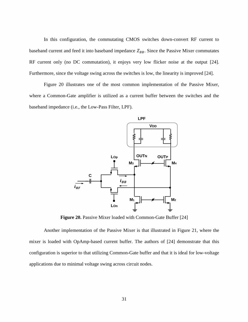
Figure 20 illustrates one of the most common implementation of the Passive Mixer,
where a Common-Gate amplifier is utilized as a current buffer between the switches and the
baseband impedance (i.e., the Low-Pass Filter, LPF).
LOp
LOn
𝒊𝑹𝑭
C
𝒊𝑩𝑩
M1 M2
M3 M4
OUTN OUTP
VDD
LPF
Figure 20. Passive Mixer loaded with Common-Gate Buffer [24]
Another implementation of the Passive Mixer is that illustrated in Figure 21, where the
mixer is loaded with OpAmp-based current buffer. The authors of [24] demonstrate that this
configuration is superior to that utilizing Common-Gate buffer and that it is ideal for low-voltage
applications due to minimal voltage swing across circuit nodes.

32
LOp
LOn
𝒊𝑹𝑭
C
𝒊𝑩𝑩
+
_+
_
OUTp
OUTN
Figure 21. Passive Mixer loaded with OpAmp-based Current Buffer [24]
In the preceding discussion, it has been assumed that the RF current is supplied by the
previous stage; e.g., a Transconductor. However, one of the advantages of the passive mixer is
that unlike the Gilbert Cell topology, it does not require a dedicated transconductor. As a matter
of fact, the LNA that drives the passive mixer acts as the Transconductor as reported in [24] and
illustrated in Figure 22.
LOp
LOn
𝒁𝑩𝑩 𝒔 /
𝑰𝑳𝒆𝒋𝝋𝑳
𝑰𝑯𝒆𝒋𝝋𝑯
𝑰𝑩𝑩𝒆𝒋𝝋𝑩𝑩 +
-
C
𝒁𝑳 𝒔
𝑰𝑹𝑭𝒆𝒋𝝋𝑹𝑭
X
Figure 22. LNA as Transconductor in Passive Mixer [24]
In this figure, the current source represents the LNA and is the tuned LC tank.
It is prudent at this stage to review the performance of the Passive Mixer as reported in
recent publications. [28] has reported IIP2 of +70dBm at the receiver input. Also, IIP3 of
+11dBm has been demonstrated by [29]. These encouraging data suggest that the Passive Mixer

33
shall be considered as the candidate for incorporation in the Reconfigurable Receiver Frontend
for Multi-Standard Radios.
34
3 Available Noise Cancellation Techniques
3.1 Introduction
CMOS-based amplifiers generally exhibit higher noise figure compared to their SiGe-
based counterparts [8]. Furthermore, the Common-Gate topology has inferior noise performance
compared to that of Common-Source. Ignoring the noise contribution due to the load, the
Common-Gate amplifier’s minimum Noise Factor is given by [8]:
(5)
Where is the excess channel thermal noise coefficient and
; with defined
as the zero-bias channel conductance.
As such, a method of minimizing the amplifier noise shall be adopted. In this chapter, we
will review the available noise cancellation techniques, and adopt the most appropriate topology
for our purpose.
3.2 Capacitive Cross-Coupling Noise Cancellation
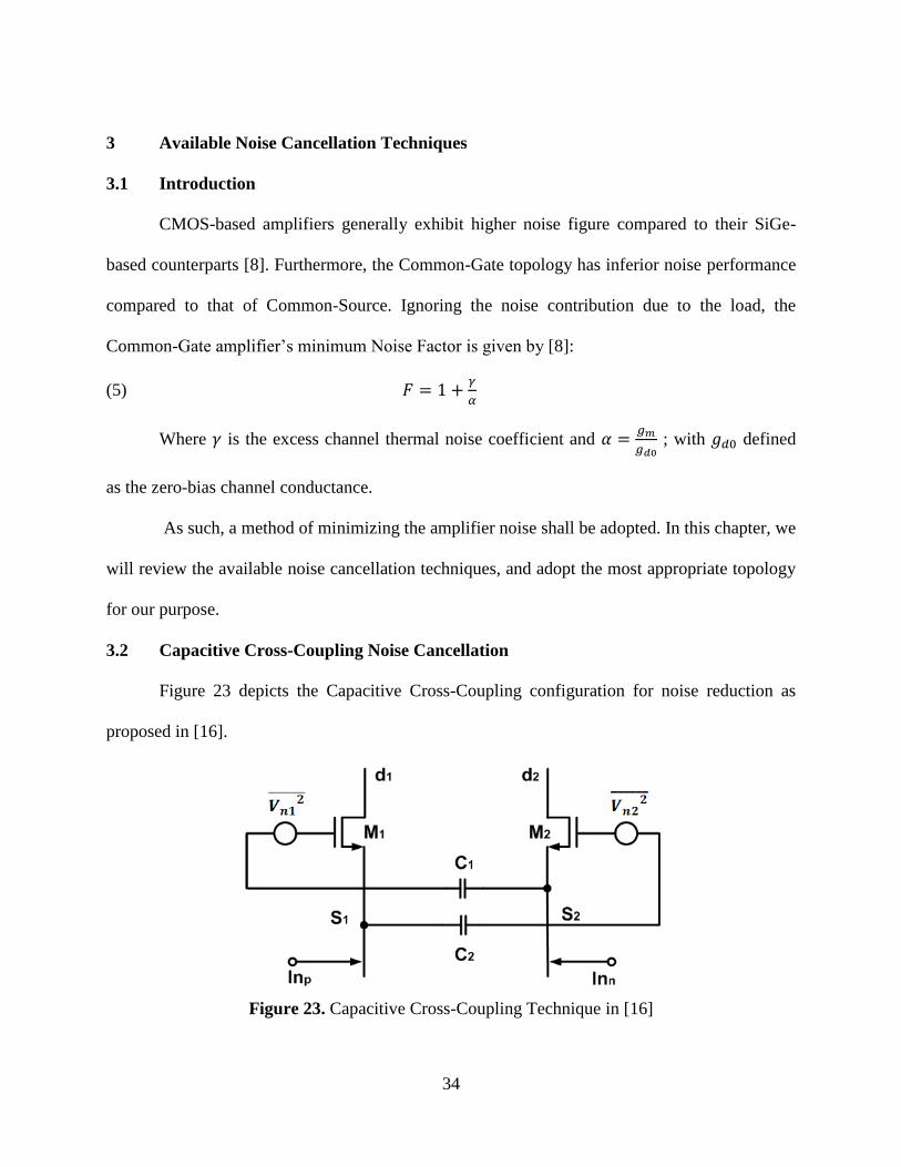
Figure 23 depicts the Capacitive Cross-Coupling configuration for noise reduction as
proposed in [16].
Figure 23. Capacitive Cross-Coupling Technique in [16]

35
Although the capacitive cross-coupling technique has been used for gain enhancement
and matching [17], our interest in this work is its noise performance improvement characteristic.
The capacitive cross-coupling causes the noise of and to produce common-mode
noise voltages at the output nodes and .
Considering only the channel thermal noise, the noise factor of the capacitive-coupled
transistors and is as follows:
(6)
Although appealing at the first glance due to number ―2‖ in the denominator, it shall be
stated that the authors of [16] utilized the capacitive cross-coupling technique in an LNA with
off-chip inductors as current source as depicted in Figure 24.
M1
Inp
M2
C1
C2
Inn
L1 L2
gnd
M3 M4VC
R1
Outn Outp
R2
gnd
Vdd
M8
M7
gnd
Vdd
M6
M5
C3
M9
Ibias
Vdd
Figure 24. LNA with Capacitive Cross-Coupling in [16]
Since one of the objectives of this work is to eliminate off-chip inductors, the Capacitive
Cross-Coupling technique shall be utilized with an on-chip transistor-based current source;

36
however, as mentioned in [16], the capacitive cross-coupling technique only addresses the noise
generated by the amplifier transistors, and does not affect the considerable noise produced by the
transistor-based current source. Had the authors utilized on-chip transistor-based current source,
the noise factor would have been as follows [3]:
(7)
Comparing equations (7) and (5), it is apparent that the capacitive cross-coupling
technique with on-chip transistor-based current source has inferior noise performance to a pure
Common-Gate amplifier.
3.3 Cross-Coupling Noise Cancellation Technique
Another technique in improving the noise performance of the LNA is that proposed in [6]
and depicted in Figure 25.
M3
M1 M2
M4
RF in
RF out
Figure 25. Cross-Coupling Noise Cancellation Technique as employed in [6]
37
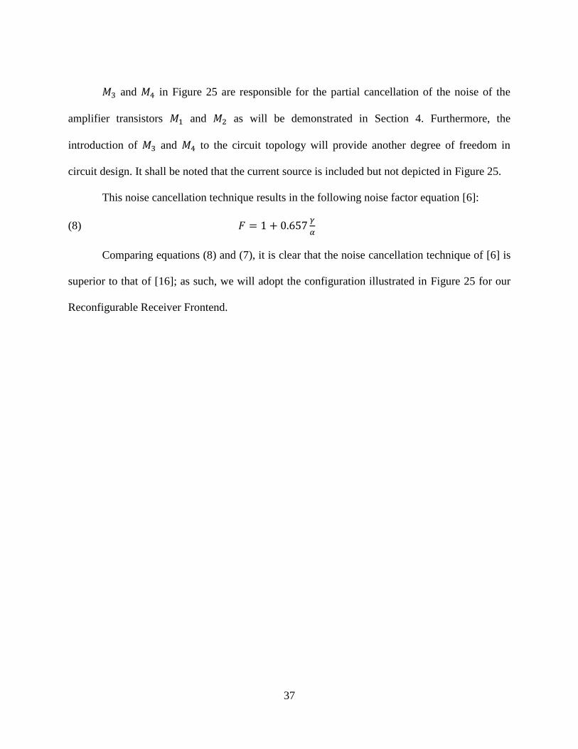
and in Figure 25 are responsible for the partial cancellation of the noise of the
amplifier transistors and as will be demonstrated in Section 4. Furthermore, the
introduction of and to the circuit topology will provide another degree of freedom in
circuit design. It shall be noted that the current source is included but not depicted in Figure 25.
This noise cancellation technique results in the following noise factor equation [6]:
(8)
Comparing equations (8) and (7), it is clear that the noise cancellation technique of [6] is
superior to that of [16]; as such, we will adopt the configuration illustrated in Figure 25 for our
Reconfigurable Receiver Frontend.

38
4 Proposed LNA Circuit Topology and its Analysis
4.1 Proposed Circuit Topology
The review of the candidate topologies for the LNA and Noise Cancellation techniques in
Sections 2 and 3 resulted in the selection of the Positive Feedback LNA of [5], as depicted in
Figure 11, and the Noise Cancellation technique of [6], as illustrated in Figure 25. Nevertheless,
as discussed in Section 2.1.3.2, the tank load of the LNA of [5] was area-hungry due to the use of
multiple inductors, and required an alternative. The alternative load tank was then determined to
be the one employed in [13], as it used only one differential inductor and dedicated parallel
capacitors for each band of interest; however, it required some modification as discussed in
Section 2.1.3.1
Figure 26 depicts the fully-differential representation of the proposed circuit topology for
the multiband LNA with positive feedback, noise cancellation circuitry, and on-chip current
source for the DSC1800, PCS1900, AWS1700, and IMT2100 frequency bands, where the
biasing network is not illustrated for simplicity.
As discussed in section 2.2.3.2, the OpAmp-based Passive Mixer was the most
appropriate topology for consideration in the Reconfigurable Receiver Frontend architecture;
however, no mixer was included in the simulation efforts of this work; as such, only the LNA
section of the Receiver Frontend is illustrated in Figure 26 and will be analyzed and simulated in
this and the following sections, respectively.

39
Vbias
M1
M2
M3 M4
M6M5
M7
Vbias
M8
VDD
Tunable Load
RFin+
RFout+ _
_
V1V1CPCS CPCS
V2V2CDCS CDCS
LDiff
VDD
VDD
Figure 26. Proposed Multiband LNA Architecture
As discussed in Section 2.1.3.2, unlike the topology in [5], the proposed LNA utilizes on-
chip current source and embeds a noise cancellation circuitry adopted from [6]. Furthermore, it
40
employs only one inductor for all frequency bands of interest. In addition, unlike the load tank
proposed in [13], and as discussed in Section 2.1.3.1, one of the bands (i.e., IMT2100) is selected
as a result of resonance of the differential inductor with the parasitic capacitance of the amplifier
transistors.
The load tank consists of the differential inductor, , the switchable capacitors,
and , and the parasitic capacitance of the input transistors.
Inductor has been sized large enough to resonate with the parasitic capacitance of
the input and feedback transistors ( and ) at the center frequency of the IMT2100, when
the band selection switches are off.
When only the PCS switch is on, Capacitor resonates with inductor at the
center frequency of the PCS1900 band to select this spectrum.
Similarly, when only the DCS switch is on, a resonance tank consisting of capacitor
and is created that passes the DCS1800 frequency band.
Since the circuit operates from a 1.2V power supply, and given the large value of the
threshold voltage of the NMOS transistors in the 0.12µm technology, PMOS transistors (i.e.,
and ) have been utilized for cross-coupling purposes.
4.2 Input Matching and Gain
The half-circuit illustration of the proposed circuit topology for the multiband LNA is
depicted in Figure 27.

41
Vs
Rs
Vbias
-1
Zin
IinI1
M1
M2
M3
I3
I2
M4
M7
Vin
ZLoad
Ibias Ibias
Vbias
X
Figure 27. Half-Circuit Topology for the Proposed Multiband LNA
We will use the circuit of Figure 27 for Transconductance Gain and Matching
calculations in this section. It shall be noted that currents , , , and are AC while is
DC. Furthermore, the current sources, as represented by , are on-chip as demonstrated in
Figure 26.
The shunt-shunt (voltage-current) positive feedback of Figure 27 has the effect of
increasing the input impedance of the simple Common-Gate amplifier as will be demonstrated
shortly.
Applying KCL at node , we obtain the following equation:
(9)
Using KVL from the Gate of to the Source of , we have:

42
(10)
Also, from Figure 27, the following may be derived:
(11)
Where may be written as follows:
(12)
However, is a function of as shown below
(13)
Combining (13), (12), and (11), we obtain the following equation for :
(14)
Assuming the output impedance of the current sources is significantly higher than , we
may write as follows:
(15)
However, since and that , may be re-written as follows:
(16)
Combining (10) and (16), we obtain the following equation for :
(17)
We are now at a position to derive by combining (9), (13), (14), and (17) as follows:
(18)
Also, from Figure 27, it is obvious that
(19)
As such, may be derived as follows:

43
(20)
Which may be simplified as follows:
(21)
Equation (21) proves the earlier statement on the effect of the positive feedback on
increasing the input impedance of the LNA.
Equation (21) also confirms that the input impedance, , is a function of the load
impedance, ; as such, if is a tunable LC tank, the input impedance will also
be tunable and purely resistive at the resonance frequency of the tank (e.g., ).
Assuming the impedance of the load at is , the input impedance at the tank
resonance frequency may be written as follows:
(22)
For input matching purposes, we must have ; therefore, the following
relationship will hold among circuit parameters at the resonance frequency of the tank.
(23)
Equation (23) confirms that for input matching, there are more degrees of freedom
compared to the simple Common-Gate LNA, where
must hold.
Nevertheless, as we will see later, will primarily be determined to minimize the
noise figure of the LNA.
Another major difference between a simple Common-Gate LNA and that employing
Positive-Feedback is concerned with the Transconductance Gain,
. In the case of

44
simple Common Gate amplifier, and under the matching condition,
.
However, with the Positive-Feedback topology, may be derived as follows at the
resonance frequency of the tank and using Figure 27 as the reference:
(24)
Combining (13), (18), and (24), we have:
(25)
Which reduces to
(26)
In matching condition, (23) holds; therefore, is equal to:
(27)
Unlike the simple Common-Gate topology, where
, in the Positive-Feedback
topology is not restricted by the source impedance, and may be determined as large as
desired to meet the gain requirement. This is another advantage of the Positive-Feedback
topology over that of simple common gate.
4.3 Noise Figure
The Common Gate amplifier exhibits worse noise performance than that of Common
Source [7]. This is the result of the input matching constraint, which requires the amplifier’s
to be equal to
; while in the case of Positive-Feedback amplifier, there is a degree of freedom

45
in the choice of . As such, the noise figure of the Positive-Feedback amplifier may be shown
to be close to that of the Inductively-degenerated Common Source amplifier [9].
We will use the half circuit of Figure 28 for the purpose of calculating the Noise Figure
of the differential circuit, where only the noise contribution of the bias current sources has been
neglected.
Rs
-1Inx
M1
M2
M3 M4
M7
Vx
VnsVn4
VnL
Rp
Vn2
Vn1
Rs
Vy
Iny
12
Figure 28. Proposed LNA core for Noise Calculation
Using the lemma proved in [10], we may write each of the noise voltages in Figure 28 as
follows:
(28)
(29)
(30)

46
(31)
(32)
Where is the transistor channel thermal noise and is a constant defined in Section 3.1.
Applying KCL to node 2, we have
(33)
Using and re-organizing (33), we obtain the following equation for :
(34)
Similarly, by applying KCL to node 2, we have
(35)
Using and re-organizing (35), we obtain the following equation for :
(36)
Replacing in (36) with its equivalent from (34), and simplifying, we obtain
(37)
Consequently, may be written as a function of as follows:
(38)
Incorporating (38) in (34), we obtain the following equation for as a function of :
(39)
In order to calculate the two output currents and due to , we use the following
equations:
(40)

47
And
(41)
Replacing in (40) with its equivalent from (38) and in (41) with its equivalent from
(39), we have
(42)
And
(43)
Finally, using the equation
, where
represents the
differential output noise power due to source impedance noise voltage (i.e., ), we have
(44)
Following similar steps for the other noise sources as depicted in Figure 28, we obtain the
following differential output noise power equations:
(45)
(46)
(47)
(48)
Where ,
, , and
are the noise power due to transistor
, transistor , transistor , and load , respectively.
48
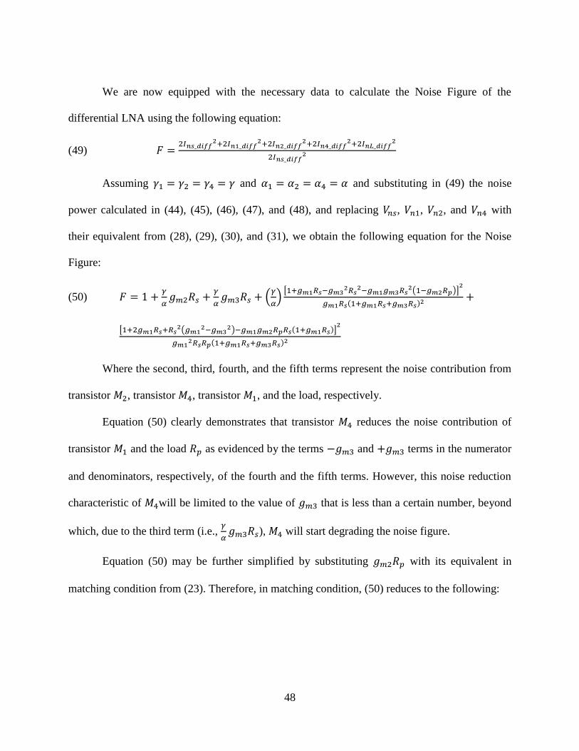
We are now equipped with the necessary data to calculate the Noise Figure of the
differential LNA using the following equation:
(49)
Assuming and and substituting in (49) the noise
power calculated in (44), (45), (46), (47), and (48), and replacing , , , and with
their equivalent from (28), (29), (30), and (31), we obtain the following equation for the Noise
Figure:
(50)
Where the second, third, fourth, and the fifth terms represent the noise contribution from
transistor , transistor , transistor , and the load, respectively.
Equation (50) clearly demonstrates that transistor reduces the noise contribution of
transistor and the load as evidenced by the terms and terms in the numerator
and denominators, respectively, of the fourth and the fifth terms. However, this noise reduction
characteristic of will be limited to the value of that is less than a certain number, beyond
which, due to the third term (i.e.,
), will start degrading the noise figure.
Equation (50) may be further simplified by substituting with its equivalent in
matching condition from (23). Therefore, in matching condition, (50) reduces to the following:

49
(51)
Equation (51) more clearly demonstrates the noise cancellation effect of ; however,
due to the complexity of the interaction among the parameters listed in (51), the optimum value
for may not be obtained analytically; as such, for a given gain requirement (i.e., ), the
simulation tool will be utilized to achieve the lowest possible . Furthermore, this equation
reveals that for improved noise performance, must be maximized reasonably, as permitted
by design and fabrication limitation.
4.4 LNA Design Parameters
The insight and the mathematical derivations obtained in Sections 4.2 and 4.3 provide for
the determination of design parameters for Gain, Matching, and Noise Performance.
Although equations (27) and (51) suggest that higher results in larger and lower
noise figure, respectively, the achievable value for is restricted by current consumption,
power supply voltage, device characteristics, and the die area limitations. As such, in this design,
attempt was made to maximize while maintaining reasonable power consumption and device
size. Table 5 illustrates the optimum device parameters that were achieved from the simulation
of the circuit in Figure 26.
Parameter Optimum Value
49.2 mS
0.645 mS
3.6 mS
Table 5. Optimum Device Parameters obtained from simulation

50
5 Simulation Results
5.1 Gain, Matching, and Isolation
5.1.1 Conversion Gain
Figure 29 and Figure 30 depict plots of the Conversion Gain of the proposed circuit
topology for all three (3) frequency bands.
Figure 29. Conversion Gain of the proposed LNA

51
Figure 30. Conversion Gain of the proposed LNA (Close up view)
As is evident from both illustrations above, the Conversion Gain of the LNA is
approximately 20dB across all three (3) frequency bands of interest.
5.1.2 Matching
Figure 31 and Figure 32 depict the input return loss of the amplifier over all three
(3) wireless frequency bands.

52
Figure 31. Input Return Loss, , of the proposed LNA

53
Figure 32. Input Return Loss, , of the proposed LNA (Close up view)
Figure 32 confirms that the circuit exhibits better than -12dB input return loss across all
three bands.
5.1.3 Isolation
Figure 33 and Figure 34 depict the isolation between the output and the input of the LNA
for the three (3) frequency bands.

54
Figure 33. Output-to-Input Isolation, , of the proposed LNA

55
Figure 34. Output-to-Input Isolation, , of the proposed LNA (Close up view)
Figure 34 confirms that the output-to-input isolation is better than -17.7dB across all
frequency bands of interest.
Since the proposed topology utilizes positive feedback, it is expected to observe spike
(degradation) in the isolation at the resonance frequency of the tank. This is confirmed and
supported by the curves in Figure 33. Nevertheless, the isolation is acceptable; as no signal will
be injected to the output and that the next stage of the Frontend Receiver; i.e., Mixer, shall and
will be designed to provide acceptable input return loss to compensate for the lower-than-usual,
but adequate, isolation at the resonance frequencies of the tank.

56
Another note worth stating here is that the Output-to-Input isolation may significantly be
improved by adopting a Cascode configuration as employed in [18]; however, in [18], off-chip
inductors are used as current source to provide head-room for the Cascode configuration. Since
elimination of the off-chip current source is one of the objectives of this work, the Cascode
configuration is not feasible for our adopted circuit topology. Furthermore, the addition of
another active device to the circuit, and in the signal path, will degrade the noise performance.
5.2 Noise Performance
5.2.1 Noise Figure
Figure 35 and Figure 36 demonstrate the Noise Figure curves for the three frequency
bands.

57
Figure 35. Noise Figure curves of the proposed LNA

58
Figure 36. Noise Figure curves of the proposed LNA (Close up view)
The Noise Figure curves illustrated in Figure 36 clearly demonstrate the contribution of
the Cross-Coupling Noise Cancellation Technique as discussed in Section 3.3. As will be seen in
the comparison Table 7, the adopted noise cancellation technique has reduced the Noise Figure
(NF) 0.5dB and 0.7dB for the DCS1800 and IMT2100, respectively, compared to the LNA
proposed in [5].
5.2.2 Minimum Noise Figure
Figure 37 and Figure 38 depict the Minimum Noise Figure curves for the three (3)
wireless bands.

59
Figure 37. Minimum Noise Figure curves of the proposed LNA
Figure 38. Minimum Noise Figure curves of the proposed LNA (Close up view)

60
The Minimum Noise Figure, , curves exhibit that the circuit Noise Figure is about
0.7dB to 0.8 dB higher than for the corresponding frequency band.
5.3 Stability Analysis
Given that the proposed LNA utilizes positive feedback, it is reasonable to verify the
stability of the amplifier under varying load and source impedances. Before we proceed with
presenting the source and load stability plots, it is instructive to re-examine (23). The
denominator of this equation must be greater than zero (0) for the circuit to be stable; as such, we
must have
(52)
Re-organizing (52), we obtain the following stability condition:
(53)
Considering the fact that is always significantly less than , and that is
less than one, the condition in (52) may be fulfilled easily.
5.3.1 Load Stability Circles
Figure 39, Figure 40, and Figure 41 depict the Load Stability Circles in the Impedance
Smith Chart for the DCS1800, PCS1900, and IMT2100 frequency bands, respectively. To
generate these plots, the frequency was swept from 100 MHz to 10 GHz with the steps size of 50
MHz.
Since and , for a 50Ω impedance system, the center of the normalized
Smith chart falls within the stable region.

61
Figure 39. Load Stability circles of the proposed LNA for the DCS1800 band.
Figure 39 demonstrates that the unstable region for the load is located in a small portion
of the chart (i.e., the area encompassed horizontally between points -0.99501 and -1.005 that is
far from the center of the chart marked by ―1‖ and not shown in the chart); as such, it is evident
that the stable operation for the DCS1800 frequency band is guaranteed for almost every load.
It shall also be noted that the stability circles in Figure 39 are for the 1.8 GHz and 1.9
GHz frequencies, with circles for other frequencies so small to be visible.

62
Figure 40. Load Stability circles of the proposed LNA for the PCS1900 band
Similar to the DCS1800 standard, the Load Stability circles for the PCS1900 frequency
band cover a very small area on the Smith chart far away from the center marked ―1‖ (not shown
in the chart); as supported by Figure 40. As such, it is evident that the stable operation for the
PCS1800 frequency band is guaranteed for almost every load.
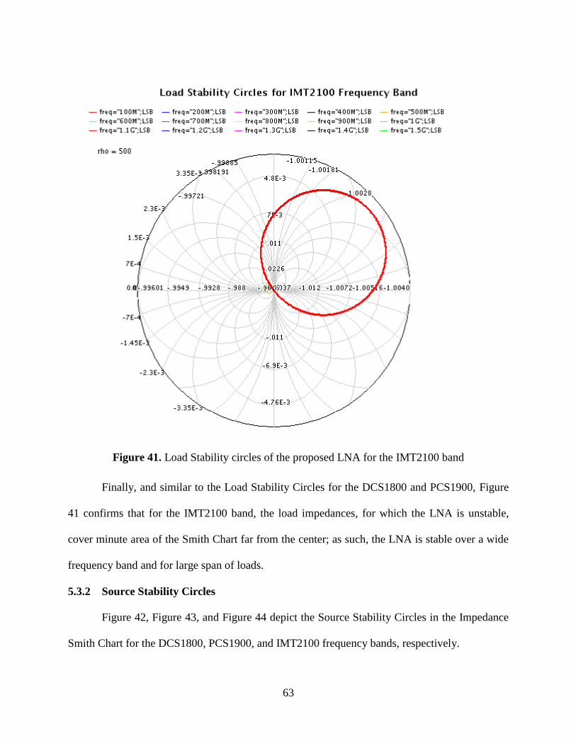
63
Figure 41. Load Stability circles of the proposed LNA for the IMT2100 band
Finally, and similar to the Load Stability Circles for the DCS1800 and PCS1900, Figure
41 confirms that for the IMT2100 band, the load impedances, for which the LNA is unstable,
cover minute area of the Smith Chart far from the center; as such, the LNA is stable over a wide
frequency band and for large span of loads.
5.3.2 Source Stability Circles
Figure 42, Figure 43, and Figure 44 depict the Source Stability Circles in the Impedance
Smith Chart for the DCS1800, PCS1900, and IMT2100 frequency bands, respectively.
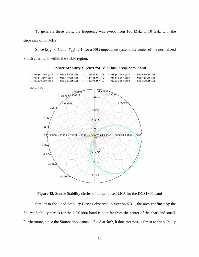
64
To generate these plots, the frequency was swept from 100 MHz to 10 GHz with the
steps size of 50 MHz.
Since and , for a 50Ω impedance system, the center of the normalized
Smith chart falls within the stable region.
Figure 42. Source Stability circles of the proposed LNA for the DCS1800 band
Similar to the Load Stability Circles observed in Section 5.3.1, the area confined by the
Source Stability circles for the DCS1800 band is both far from the center of the chart and small.
Furthermore, since the Source impedance is fixed at 50Ω, it does not pose a threat to the stability
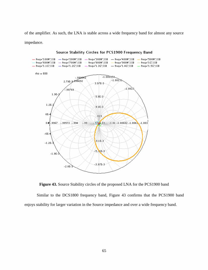
65
of the amplifier. As such, the LNA is stable across a wide frequency band for almost any source
impedance.
Figure 43. Source Stability circles of the proposed LNA for the PCS1900 band
Similar to the DCS1800 frequency band, Figure 43 confirms that the PCS1900 band
enjoys stability for larger variation in the Source impedance and over a wide frequency band.

66
Figure 44. Source Stability circles of the proposed LNA for the IMT2100 band
Finally, the Source stability circles for the IMT2100 band cover a minute area of the
Smith chart and guarantee stability under large source impedance variation and wide frequency
span.
In conclusion, the LNA is stable over the frequency band of 100 MHz to 10 GHz and for
almost any source and load impedance.
5.4 Linearity Analysis
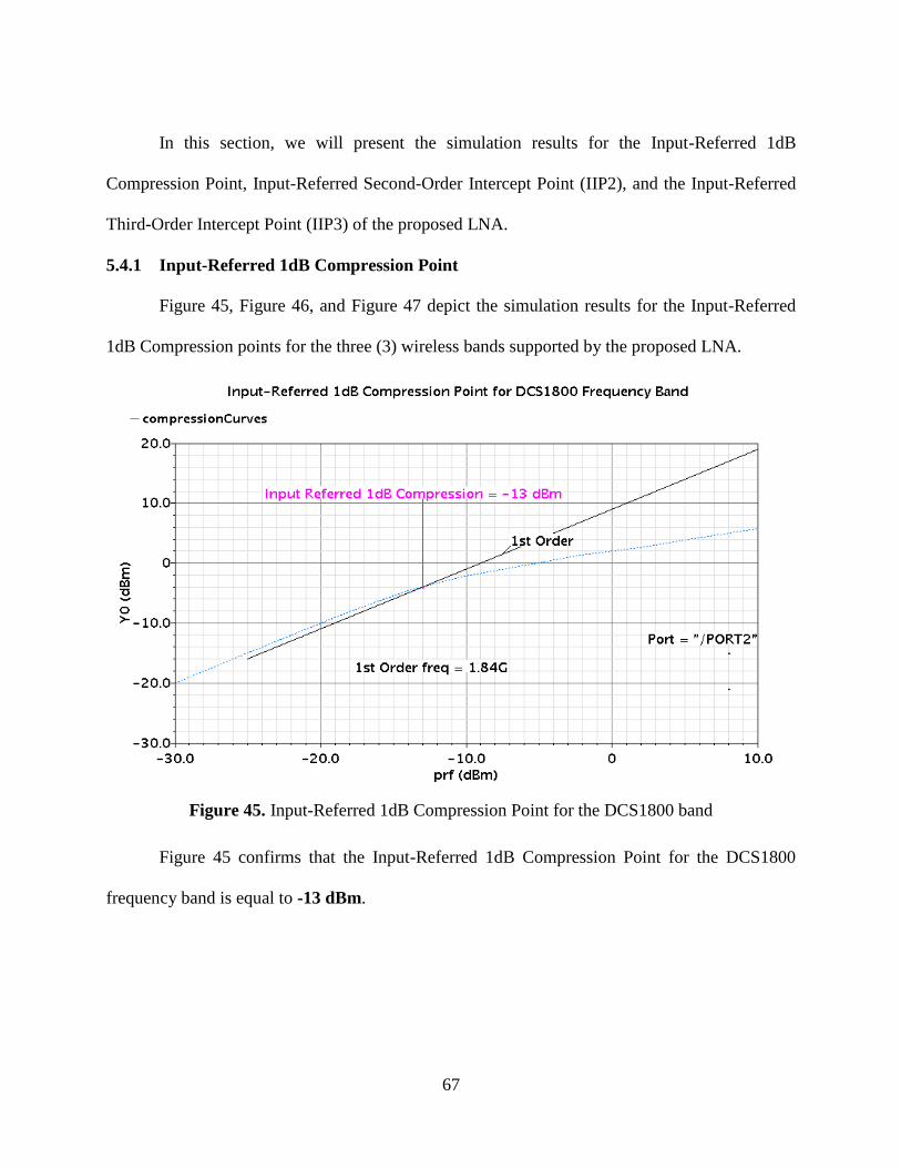
67
In this section, we will present the simulation results for the Input-Referred 1dB
Compression Point, Input-Referred Second-Order Intercept Point (IIP2), and the Input-Referred
Third-Order Intercept Point (IIP3) of the proposed LNA.
5.4.1 Input-Referred 1dB Compression Point
Figure 45, Figure 46, and Figure 47 depict the simulation results for the Input-Referred
1dB Compression points for the three (3) wireless bands supported by the proposed LNA.
Figure 45. Input-Referred 1dB Compression Point for the DCS1800 band
Figure 45 confirms that the Input-Referred 1dB Compression Point for the DCS1800
frequency band is equal to -13 dBm.

68
Figure 46. Input-Referred 1dB Compression Point for the PCS1900 band
Figure 46 confirms that, similar to the DCS1800 band, the Input-Referred 1dB
Compression Point for the PCS1900 frequency band is equal to -13 dBm.

69
Figure 47. Input-Referred 1dB Compression Point for the IMT2100 band
Finally, Figure 47 confirms that the Input-Referred 1dB Compression Point for the
IMT2100 frequency band is equal to -12.6 dBm.
The Input-Referred 1dB Compression Point figures for the frequency bands of interest
confirm that the LNA enjoys high linearity due, in part, to the configuration adopted; i.e.,
Common-Gate, as well as the Feedback and the narrow-band tuned tank.
5.4.2 Input-Referred Second-Order Intercept Point (IIP2)
Figure 48, Figure 49, and Figure 50 depict the simulation results for the Input-Referred
Second-Order Intercept Point (IIP2) for the three (3) wireless bands supported by the proposed
LNA.

70
Figure 48. Input-Referred IP2 of the proposed LNA for the DCS1800 band
Figure 48 confirms that the Input-Referred IP2 for the DCS1800 frequency band is equal
to +67 dBm. This high IIP2 is owed to the highly frequency-selective nature of the tuned tank as
evident in Figure 29.

71
Figure 49. Input-Referred IP2 of the proposed LNA for the PCS1900 band
Similar to the DCS1800 frequency band, Figure 49 confirms that the Input-Referred IP2
for the PCS1900 frequency band is high and equal to +66.5 dBm due to the same characteristics
of the LNA as mentioned above.

72
Figure 50. Input-Referred IP2 of the proposed LNA for the IMT2100 band
Finally, and similar to the other frequency bands, Figure 50 confirms that the Input-
Referred IP2 for the IMT2100 frequency band is equal to +65.5 dBm.
5.4.3 Input-Referred Third-Order Intercept Point (IIP3)
Figure 51, Figure 52, and Figure 53 depict the simulation results for the Input-Referred
IP3 for the three (3) wireless bands supported by the proposed LNA.

73
Figure 51. Input-Referred IP3 of the proposed LNA for the DCS1800 band
Figure 51 confirms that the Input-Referred IP3 for the DCS1800 frequency band is equal
to -2.3 dBm. This significant IIP3 is achieved due to the adoption of the Common-Gate topology
and maintaining the Loop Gain of the Feedback network as small as possible [5]. This is evident
from the small transconductance value of the feedback transistor as listed in Table 5.
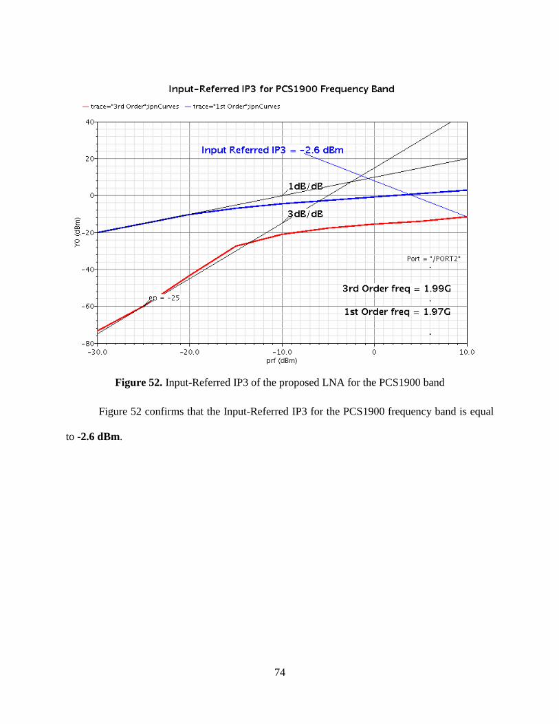
74
Figure 52. Input-Referred IP3 of the proposed LNA for the PCS1900 band
Figure 52 confirms that the Input-Referred IP3 for the PCS1900 frequency band is equal
to -2.6 dBm.
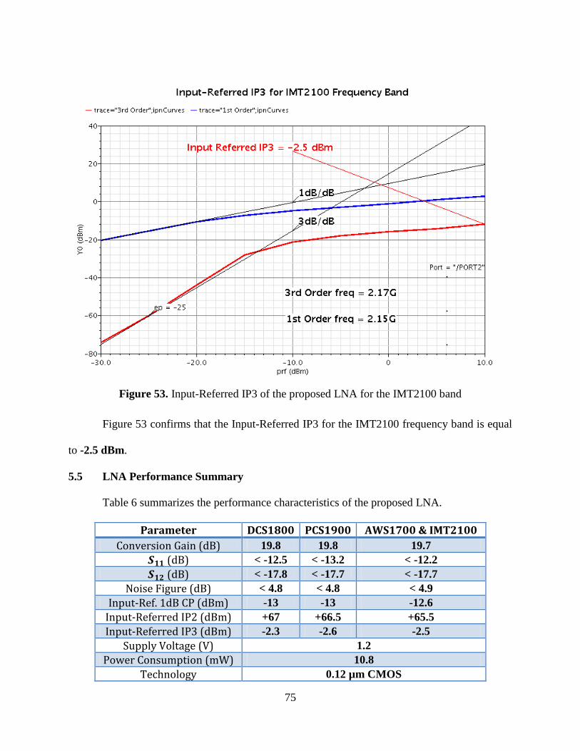
75
Figure 53. Input-Referred IP3 of the proposed LNA for the IMT2100 band
Figure 53 confirms that the Input-Referred IP3 for the IMT2100 frequency band is equal
to -2.5 dBm.
5.5 LNA Performance Summary
Table 6 summarizes the performance characteristics of the proposed LNA.
Parameter DCS1800 PCS1900 AWS1700 & IMT2100
Conversion Gain (dB) 19.8 19.8 19.7
(dB) < -12.5 < -13.2 < -12.2
(dB) < -17.8 < -17.7 < -17.7
Noise Figure (dB) < 4.8 < 4.8 < 4.9
Input-Ref. 1dB CP (dBm) -13 -13 -12.6
Input-Referred IP2 (dBm) +67 +66.5 +65.5
Input-Referred IP3 (dBm) -2.3 -2.6 -2.5
Supply Voltage (V) 1.2
Power Consumption (mW) 10.8
Technology 0.12 µm CMOS

76
Table 6. Performance Characteristics of the Proposed LNA
We are now at a position to compare the performance of the proposed LNA with that
reported in [5].
5.6 Performance Comparison
Table 7 provides the comparison of the performance characteristics of the proposed LNA
with those reported in [5].
Parameter
This Work As reported by [5]
DCS1800 PCS1900 AWS1700
& IMT2100
DCS1800 IMT2100 802.11
b-g
Conversion Gain (dB)
19.8 19.8 19.7 13.5 -
28.5
14.5 –
29.5
8.4 –
23.4
(dB) < -12.5 < -13.2 < -12.2 -32 -20 -20
(dB) < -17.8 < -17.7 < -17.7 N/A N/A N/A
Noise Figure (dB) < 4.8 < 4.8 < 4.9 5.2 5.6 5.8
Input-Ref. 1dB CP (dBm)
-13 -13 -12.6 N/A N/A N/A
Input-Referred IP2 (dBm)
+67 +66.5 +65.5 50 51 54
Input-Referred IP3 (dBm)
-2.3 -2.6 -2.5 -7.5 0 -4.8
Supply Voltage (V)
1.2 1.5
Power Consumption
(mW) 10.8 20/24
Technology 0.12 µm CMOS 0.13 µm CMOS
Table 7. Comparison of the Performance Characteristics with [5]
Table 7 demonstrates that the proposed LNA, in addition to utilizing on-chip current
source and only one inductor for all three bands of interest, is superior to that proposed in [5] in
the following areas: Noise Figure, IIP2, IIP3, Supply Voltage, Power Consumption, and the
feature size of the CMOS technology.

77
These advantages of the proposed LNA make it a good candidate for utilization in the
Frontend of a Reconfigurable Receiver for the Cellular Frequency Bands.
78
6 Conclusion and Future Work
6.1 Conclusion
This document presented the review and analysis of the state-of-the-art Receiver
Frontend Architectures for wireless communications, and identified the most appropriate
topology for Reconfigurable Multi-Standard applications.
Furthermore, the topology of a multi-band and reconfigurable LNA was introduced and
its performance was analyzed theoretically and verified by simulation. The proposed LNA
topology utilizes positive feedback for increasing gain and providing flexibility in matching,
cross-coupling configuration for noise cancellation, and on-chip current source. The LNA
supports the three major mobile wireless bands; i.e., DCS1800 (primarily in Europe and Asia),
PCS1900 (mostly in the Americas), AWS1700 (in North America), and IMT2100 (the rest of the
world) for global roaming.
6.2 Future Work
There are several areas of research and simulation work that could follow the current
effort.
One such area is the implementation of the Passive Mixer in order to verify the
performance of the combined LNA and Mixer against the pertinent regulatory standards and
provide a fair comparison with the performance reported in other publications; especially in the
areas of IIP2 and IIP3, which are heavily affected by the second stage characteristics.
Furthermore, the IIP3 and the Output-to-Input isolation are areas of importance that
require further attention and improvement. IIP3 may be improved by increasing the Overdrive
Voltage [5]. However, with on-chip current source and supply voltage of only 1.2V, it is
challenging, if not impossible. Furthermore, the Output-to-Input isolation improvement may be
79
achieved by adopting Cascode configuration; however, with on-chip current source and the 1.2V
supply voltage, it is extremely difficult. As such, a higher-voltage power supply architecture will
be investigated; potentially using start-up circuits to prevent the circuit elements from exposure
to higher-than-recommended voltage levels and not affect device reliability.
It is also warranted to investigate techniques to improve the noise figure of the proposed
LNA to levels near or below 3dB. The topology in [18] achieves lower noise figure primarily
because of utilizing positive and negative feedback networks concurrently as well as off-chip
inductors that is in contrast to the objective of this work. Had the [18] used on-chip current
source in place of off-chip inductors, its reported Noise Figure would have been higher, as no
noise cancellation technique is employed.

80
References
[1] CDMA Development Group. www.cdg.org.
[2] GSM Association. www.gsmworld.com.
[3] S. Lou and H. C. Luong, ―A 0.8GHz–10.6GHz SDR Low-Noise Amplifier in 0.13-μm
CMOS‖ IEEE 2008 Custom Integrated Circuits Conference (CICC).
[4] P. Rossi, A. Liscidini, M. Brandolini, and F. Svelto, ―A variable gain RF front-end, based
on a voltage-voltage feedback LNA, for multistandard applications,‖ IEEE J. Solid-State
Circuits, vol. 40, no. 3, pp. 690–697, Mar. 2005.
[5] A. Liscidini, M. Brandolini, D. Sanzogni, and R. Castello, ―A 0.13µm CMOS front-end
for DCS1800/UMTS/802.11b-g with multi-band positive feedback low noise amplifier,‖
IEEE J. Solid-State Circuits, vol. 41, no. 4, pp. 981–989, Apr. 2006.
[6] A. Amer, E. Hegazi, and H. F. Ragaie, ―A 90-nm Wideband Merged CMOS LNA and
Mixer Exploiting Noise Cancellation,‖ IEEE J. Solid-State Circuits, vol. 42, no. 2, pp.
323–328, Feb. 2007.
[7] H. Hashemi and A. Hajimiri, ―Concurrent Multiband Low-Noise Amplifiers—Theory,
Design, and Applications,‖ IEEE Transactions on Microwave Theory and Techniques,
vol. 50, no. 1, pp. 288-301, Jan. 2002.
[8] D. K. Shaeffer and T. H. Lee, ―A 1.5-V, 1.5-GHz CMOS low noise amplifier,‖ IEEE J.
Solid-State Circuits, vol. 32, no. 5, pp. 745–759, May 1997.
[9] A. Liscidini, M. Brandolini, P. Rossi, F. Torrisi, and F. Svelto, ―Design methodology of
feedback-LNAs for GHz applications,‖ in Proc. Bipolar/BiCMOS Circuits and
Technology Meeting (BCTM), Sep. 13–14, 2004, pp. 253–256.
[10] B. Razavi, Design of Analog CMOS Integrated Circuits, New York: McGraw-Hill, 2001.
[11] F. Bruccoleri, E. A. M. Klumperink, and B. Nauta, ―Wide-band CMOS low-noise
amplifier exploiting thermal noise canceling,‖ IEEE J. Solid-State Circuits, vol. 39, no. 2,
pp. 275–282, Feb. 2003.
[12] Adiseno, M. Ismail, and H. Olsson, ―A wide-band RF front-end for multiband
multistandard high-linearity low-IF wireless receivers,‖ IEEE J. Solid-State Circuits, vol.
37, no. 9, pp. 1162–1168, Sep. 2002.
[13] P. Rossi, A. Liscidini, M. Brandolini, and F. Svelto, ―A 2.5 dB NF direct conversion
receiver front-end for HiperLAN2/IEEE802.11a,‖ in IEEE Int. Solid-State Circuits Conf.
(ISSCC) Dig. Tech. Papers, vol. 1, Feb. 2004, pp. 102–103.

81
[14] D. J. Allstot, X. Li, and S. Shekhar, ―Design considerations for CMOS low-noise
amplifiers,‖ in Proc. IEEE Radio Frequency Integrated Circuits (RFIC) Symp., Jun.
2004, pp. 97–100.
[15] D. Cassan, J. Long, ―A 1V Transformer Feedback Low-Noise Amplifier for 5GHz
Wireless LAN in 0.18μm CMOS,‖ IEEE J. Solid-State Circuits, vol. 38, pp. 427-435,
Mar. 2003.
[16] W. Zhuo, S. Embabi, J. P. de Gyvez, and E. Sanchez-Sinencio, ―Using capacitive cross-
coupling technique in RF low noise amplifiers and down-conversion mixer design,‖
European Solid-State Circuits Conf., pp. 77-80, Sep. 2000.
[17] T. Cho et al, ―A Single-Chip CMOS Direct-Conversion Transceiver for 900MHz Spread-
Spectrum Digital Cordless Phones,‖ ISSCC Digest of Technical Papers, Feb 1999, pp.
228-229.
[18] A. Liscidini et al., ―Analysis and Design of Configurable LNAs in Feedback Common-
Gate Topologies,‖ IEEE Transactions on Circuits and Systems—II: Express Briefs, vol.
55, no. 8, August 2008.
[19] M. Brandolini et al., ―Reconfigurable Si RF Receiver Front-Ends for Multi-Standard
Radios,‖ Proceedings of the 1st European Wireless Technology Conference, October
2008, pp. 33-36.
[20] M. Brandolini, et al., ―Towards Multi-Standard Mobile Terminals: Fully Integrated
Receivers Requirements and Architectures,‖ IEEE Transactions on Microwave Theory
and Techniques, February 2005.
[21] Digital Cellular Telecommunications System (Phase 2); Radio Transmission and
Reception, GSM Standard 05 05, 1999.
[22] J. Ryynanen, et al., ―A Single-Chip Multimode Receiver for GSM900, DCS1800,
PCS1900, and WCDMA‖, IEEE Journal of Solid State Circuits, vol.38, n.4, pp.594-602,
April 2003.
[23] M. Brandolini, et al., ―A +78 dBm IIP2 CMOS Direct Downconversion Mixer for Fully
Integrated UMTS Receivers,‖ IEEE J. Solid-State Circuits, vol. 41, no. 3, pp. 552-559,
March 2006.
[24] H. Darabi, et al., ―Analysis and Optimization of Current-Driven Passive Mixers in
Narrowband Direct-Conversion Receivers,‖ IEEE J. Solid-State Circuits, vol. 44, no. 10,
pp. 2678-2688, October 2009.
[25] P. Cruz, et al., ―Designing and Testing Software-Defined Radios,‖ IEEE Microwave
Magazine, pp. 83-94, June 2010.

82
[26] D. Manstretta, et al., ―Second-order inter-modulation mechanisms in CMOS
downconverters,‖ IEEE J. Solid-State Circuits, vol. 38, no. 3, pp. 394–406, Mar. 2003.
[27] M. Brandolini, et al., ―A 0.18 μm CMOS direct down-converter for highly integrated 3G
receivers,‖ Analog Integrated Circuit Signal Processing, pp. 35-42, 2007.
[28] J. Borremans, et al., ―A 40nm CMOS Highly Linear 0.4-to-6GHz Receiver Resilient to
0dBm Out-of-Band Blockers,‖ in IEEE Int. Solid-State Circuits Conf. (ISSCC) Dig. Tech.
Papers, Session 3, Feb. 2011, pp. 62–64.
[29] M. C. M. Soer, et al., ―A 0.2-to-2.0GHz 65nm CMOS Receiver Without LNA Achieving
>11dBm IIP3 and <6.5 dB NF,‖ in IEEE Int. Solid-State Circuits Conf. (ISSCC) Dig.
Tech. Papers, Session 12, Feb. 2009, pp. 222-224.


