
Scanning Tunneling Spectroscopy Studies on
Strongly Disordered S-Wave Superconductors
Close To Metal Insulator Transition
A Thesis
Submitted to the
Tata Institute of Fundamental Research, Mumbai
for the degree of Doctor of Philosophy
in Physics
by
ANAND KAMLAPURE
Department of Condensed Matter Physics and Materials Science
Tata Institute of Fundamental Research
Mumbai
April, 2014
Final Version Submitted in August, 2014


To my parents

DECLARATION
This thesis is a presentation of my original research work.
Wherever contributions of others are involved, every effort is
made to indicate this clearly, with due reference to the literature,
and acknowledgement of collaborative research and discussions.
The work was done under the guidance of Professor Pratap
Raychaudhuri, at the Tata Institute of Fundamental Research,
Mumbai.
Anand Kamlapure
In my capacity as supervisor of the candidate’s thesis, I certify
that the above statements are true to the best of my knowledge.
Prof. Pratap Raychaudhuri
Date:

STATEMENT OF JOINT WORK
The experiments reported in this thesis have been carried out in the Department
of Condensed Matter Physics and Material Science under the guidance of Prof. Pratap
Raychaudhuri. The results of the major portions of the work presented in this thesis
have already been published in refereed journals.
Most of the experiments discussed in this thesis have been conducted by me in
the department. For completeness, I have included some of the experiments and data
analysis performed by other group members and collaborators.
Some of the scanning tunneling measurements were carried out jointly with
Garima Saraswat and Somesh Chandra Ganguli. Transport, Magnetoresistance and
Hall effect measurements were carried out in collaboration with Madhavi Chand.
Penetration depth measurements were carried out by Mintu Mondal and Sanjeev
Kumar. All the Transmission Electron Microscope measurements were carried out by
Tanmay Das and Somnath Bhattacharyya. Theoretical work was done in collaboration
with Dr. Vikram Tripathi of Department of Theoretical Physics, TIFR and Dr. Lara
Benfatto and Dr. Gabriel Lemarié of University of Rome, Rome, Italy.
PREFACE
The work presented in this thesis is on the experimental investigation of the
effect of disorder on s-wave superconductor NbN through scanning tunneling
spectroscopy (STS) measurements.
Disorder induced superconductor insulator transition (SIT) has been the subject
of interest since decades and there have been major advances both experimentally and
theoretically in understanding the nature of SIT. Recently new insights have been
offered by the numerical simulations which predicts unprecedented phenomena such
as persistence of gap across the SIT, spatial inhomogeneity in the gap and order
parameter, emergence of superconductivity over much larger length scale than the
disorder length scale, which needs to be addressed through sophisticated experiments.
The work presented in this thesis unravels many of these novel phenomena near the
SIT in s-wave superconductor, NbN, primarily through scanning tunneling
spectroscopy measurements and supported by results of penetration depth and transport
measurements.
The thesis is organized in following way, In Chapter 1, I will introduce the
motivation for our experiments on disordered superconductors through the advances in
the experimental and theoretical works. I will also introduce our model system: NbN
as a perfect system and its characterization through transmission electron microscope
at the atomic scale. In Chapter 2, I will elaborate on the basics of scanning tunneling
microscope (STM), fabrication of low temperature STM, related techniques and the
scheme of measurements. Chapter 3 focuses on our observation of formation of
pseudogap state in NbN in presence of strong disorder. We argue that the phase
fluctuation is the possible mechanism for the formation of pseudogap state. In Chapter
4, we investigate the ground state superconducting properties in strongly disordered
NbN through spatially resolved STS measurements. We identify that the coherence
peak height is a measure of local order parameter and show that the superconductivity
in the disordered NbN emerges over tens of nanometer scale while the structural
disorder present in the system is at atomic scale. In this chapter we also show that the
order parameter distribution in strongly disordered NbN has a universal behaviour
irrespective of the strength of disorder present in the system. We end the chapter with
the temperature evolution of inhomogeneous superconducting state through spatially
resolved STS measurements. In the concluding Chapter 5, I will summarize all our
investigation during past 6 years and present a phase diagram showing evolution of
various energy scales with disorder.

ACKNOWLEDGEMENTS
First and foremost, I would like to express my sincere gratitude to my thesis
advisor Prof. Pratap Raychaudhuri for the continuous support for my PhD work, for his
patience, motivation and enthusiasm.
I thank my fellow lab mates Garima Saraswat, Madhavi Chand, Mintu Mondal,
Sanjeev Kumar, Archana Mishra, Somesh Chandra Ganguli, Rini Ganguly, Harkirat
Singh, Prashant Shirage, John Jesudasan and Vivas Bagwe for their constant help and
support in every regard.
My sincere thanks goes to Subash Pai from Excel Instruments for all the prompt
technical support. I also thank Bhagyashree (Shilpa) Chalke, Rudhir Bapat, Nilesh
Kulkarni for the help in characterizing the samples and Atul Raut for technical help.
Most importantly I thank Low Temperature Facility team of TIFR for continuous
supply of liquid He and Nitrogen.
I also thank Vikram Tripathi, Lara Benfatto, Gabriel Lemarié for all the
discussions and theoretical support.
I take the opportunity to thank all my friends for their support, motivation and
all the fun we had during my Phd, especially I would like mention Sachin, Jaysurya,
Ajith, Gajendra, Abhishek, Nilesh, Harshad, Nikesh, Ashish, Amlan, Laskar, Bhanu,
Pranab, Abhishek, Mohon, Ronjoy, Sayanti, Anuj, Shishram, Vinod, Subhash, Amar,
Sunil, Abhijeet, Vinod, Jay, Jay, Sanjiv, Onkar, Shireen, Amul, Rajkiran, Lasse and
Pavel.
I finally thank my family members for their love and patience and I dedicate
this thesis to my parents.
LIST OF PUBLICATIONS
In refereed Journal and related to material presented here.
1. Emergence of nanoscale inhomogeneity in the superconducting state of a
homogeneously disordered conventional superconductor
Anand Kamlapure, Tanmoy Das, Somesh Chandra Ganguly, Somnath
Bhattacharya and Pratap Raychaudhuri
Scientific Reports 3 , 2979 (2013).
2. A 350 mK, 9 T scanning tunneling microscope for the study of superconducting
thin films and single crystals
Anand Kamlapure, Garima Saraswat, Somesh Chandra Ganguli, Vivas Bagwe,
Pratap Raychaudhuri and Subash P. Pai
Rev. Sci. Instrum. 84, 123905.
3. Universal scaling of the order-parameter distribution in strongly disordered
superconductors
G. Lemarié, A. Kamlapure, D. Bucheli, L. Benfatto, J. Lorenzana, G. Seibold, S.
C. Ganguli, P. Raychaudhuri and C. Castellani
Phys. Rev. B 87, 184509 (2013).
4. Phase diagram of the strongly disordered s-wave superconductor NbN close to the
metal-insulator transition
Madhavi Chand, Garima Saraswat, Anand Kamlapure, Mintu Mondal, Sanjeev
Kumar, John Jesudasan, Vivas Bagwe, Lara Benfatto, Vikram Tripathi, and Pratap
Raychaudhuri
Phys. Rev. B 85, 014508 (2012).
5. Phase Fluctuations in a Strongly Disordered s-Wave NbN Superconductor Close to
the Metal-Insulator Transition
Mintu Mondal, Anand Kamlapure, Madhavi Chand, Garima Saraswat, Sanjeev
Kumar, John Jesudasan, L. Benfatto, Vikram Tripathi, and Pratap Raychaudhuri
Phys. Rev. Lett. 106, 047001 (2011).
6. Enhancement of the finite-frequency superfluid response in the pseudogap regime
of strongly disordered superconducting films
Mintu Mondal, Anand Kamlapure, Somesh Chandra Ganguli, John Jesudasan,
Vivas Bagwe, Lara Benfatto and Pratap Raychaudhuri
Scientific Reports 3, 1357 (2013).
7. Temperature dependence of resistivity and Hall coefficient in strongly disordered
NbN thin films
Madhavi Chand, Archana Mishra, Y. M. Xiong, Anand Kamlapure, S. P.
Chockalingam, John Jesudasan, Vivas Bagwe, Mintu Mondal, P. W. Adams,
Vikram Tripathi, and Pratap Raychaudhuri
Phys. Rev. B 80, 134514 (2009).
8. Tunneling studies in a homogeneously disordered s-wave superconductor: NbN
S. P. Chockalingam, Madhavi Chand, Anand Kamlapure, John Jesudasan, Archana
Mishra, Vikram Tripathi, and Pratap Raychaudhuri
Phys. Rev. B 79, 094509 (2009).
In refereed journals, not related to the work presented
here.
1. Measurement of magnetic penetration depth and superconducting energy gap in
very thin epitaxial NbN films
Anand Kamlapure, Mintu Mondal, Madhavi Chand, Archana Mishra, John
Jesudasan, Vivas Bagwe, L. Benfatto, Vikram Tripathi, and Pratap Raychaudhuri
Appl. Phys. Lett. 96, 072509 (2010).
2. Andreev bound state and multiple energy gaps in the noncentrosymmetric
superconductor, BiPd
Mintu Mondal, Bhanu Joshi, Sanjeev Kumar, Anand Kamlapure, Somesh Chandra
Ganguli, Arumugam Thamizhavel, Sudhansu S. Mandal, Srinivasan Ramakrishnan
and Pratap Raychaudhuri
Phys. Rev. B 86 (9), 094520 (2012).
3. Role of the Vortex-Core Energy on the Berezinskii-Kosterlitz-Thouless Transition
in Thin Films of NbN
Mintu Mondal, Sanjeev Kumar, Madhavi Chand, Anand Kamlapure, Garima
Saraswat, G. Seibold, L. Benfatto, and Pratap Raychaudhuri
Phys. Rev. Lett. 107, 217003 (2011).
Conference Proceedings
1. Pseudogap state in strongly disordered conventional superconductor, NbN
Anand Kamlapure, Garima Saraswat, Madhavi Chand, Mintu Mondal, Sanjeev
Kumar, John Jesudasan, Vivas Bagwe, Lara Benfatto, Vikram Tripathi and Pratap
Raychaudhuri
J. Phys.: Conf. Ser. 400 022044 (2012).
2. Study of Pseudogap State in NbN using Scanning Tunneling Spectroscopy
Madhavi Chand, Anand Kamlapure, Garima Saraswat, Sanjeev Kumar, John
Jesudasan, Mintu Mondal, Vivas Bagwe, Vikram Tripathi, Pratap Raychaudhuri.
AIP Conference Proceedings 1349, 61.
3. Upper Critical Field and Coherence Length of Homogenously Disordered Epitaxial
3-Dimensional NbN Films
John Jesudasan, Mintu Mondal, Madhavi Chand, Anand Kamlapure, Sanjeev
Kumar, Garima Saraswat, Vivas C Bagwe, Vikram Tripathi, Pratap Raychaudhuri
AIP Conference Proceedings 1349, 923.
4. Magnetoresistance studies of homogenously disordered 3-dimensional NbN thin
films
Madhavi Chand, Mintu Mondal, Sanjeev Kumar, Anand Kamlapure, Garima
Saraswat, SP Chockalingam, John Jesudasan, Vivas Bagwe, Vikram Tripathi, Lara
Benfatto, Pratap Raychaudhuri
Journal of Physics: Conference Series 391 (1), 012086.
5. Evolution of Kosterlitz-Thouless-Berezinskii (BKT) Transition in Ultra-Thin NbN
Films
Mintu Mondal, Sanjeev Kumar, Madhavi Chand, Anand Kamlapure, Garima
Saraswat, Vivas C Bagwe, John Jesudasan, Lara Benfatto, Pratap Raychaudhuri
Journal of Physics: Conference Series 400 (2), 022078.
6. Effect of Phase Fluctuations on the Superconducting Properties of Strongly
Disordered 3D NbN Thin Films
Madhavi Chand, Mintu Mondal, Anand Kamlapure, Garima Saraswat, Archana
Mishra, John Jesudasan, Vivas C Bagwe, Sanjeev Kumar, Vikram Tripathi, Lara
Benfatto, Pratap Raychaudhuri
Journal of Physics: Conference Series 273 (1), 012071.
TABLE OF CONTENTS
Synopsis ............................................................................................... 21
Chapter 1 ............................................................................................. 43
1.1 Basics of Superconductivity ........................................................................... 45
1.1.A The Meissner-Ochsenfeld effect ......................................................... 45
1.1.B The London equations ............................................................................. 45
1.1.C Nonlocal Response: Pippard Coherence length ( ξ0 ) ............... 46
1.1.D Ginzburg Landau (G-L) model of superconductivity ................ 47
Phase stiffness ............................................................................ 48
G-L Characteristic length scales ................................................ 48
Type I and Type II superconductors .......................................... 49
1.1.E BCS theory of superconductivity ........................................................ 50
The gap function ........................................................................ 51
Temperature dependence of the gap and Tc............................. 51
BCS density of states .................................................................. 52
1.1.F Electron tunneling and measurement of ∆ .................................... 53
1.2 Disordered Superconductors ........................................................................ 54
1.3 Our model system: NbN ................................................................................... 56
1.3.A Sample growth and introducing disorder...................................... 56
1.3.B Structural characterization of NbN films ....................................... 57
1.3.C Quantification of disorder ...................................................................... 58
1.4 Effects of disorder .............................................................................................. 58
1.4.A Resistivity and measurement of Tc.................................................... 59
1.4.B Hall carrier density measurement ..................................................... 60
1.4.C Upper critical field (Hc2) and coherence length (ξGL) ................ 61
1.4.D Magnetic penetration depth (λ).......................................................... 61
1.5 References .............................................................................................................. 62
Chapter 2 ............................................................................................. 68
2.1 Schematic of STM ................................................................................................ 69
2.1.A Constant current mode ........................................................................... 70
2.1.B Constant height mode .............................................................................. 71
2.2 STM Theory ............................................................................................................71
2.2.A Tersoff–Hamann formalism ..................................................................74
2.2.B Other models ................................................................................................75
2.3 Fabrication of low temperature STM ........................................................76
2.3.A STM Head .......................................................................................................78
Coarse positioner: ...................................................................... 78
Piezoelectric tube ...................................................................... 80
Mechanical Description of the STM head ................................. 81
Calibration of Piezo constants ................................................... 83
Tip preparation .......................................................................... 84
2.3.B Sample holder ..............................................................................................85
2.3.C Sample Preparation chamber ...............................................................87
2.3.D Load lock and sample manipulators .................................................88
2.3.E 3He Cryostat ..................................................................................................89
Variable temperature insert ...................................................... 89
Liquid Helium Dewar ................................................................. 90
Temperature control of the sample .......................................... 91
2.3.F Vibrational and electrical noise reduction .....................................91
Vibrational noise ........................................................................ 91
Electrical noise ........................................................................... 93
Characterization of noise ........................................................... 94
2.4 Experimental Methods and results.............................................................94
2.4.A Topography ...................................................................................................94
2.4.B Scanning tunneling spectroscopy (STS) ..........................................95
Normal Superconductor tunneling ............................................ 97
2.4.C Linescan ..........................................................................................................98
2.4.D Spatially resolved STS and conductance map ..............................99
Conductance map ...................................................................... 99
2.5 Reference ............................................................................................................. 101
Chapter 3 ........................................................................................... 106
3.1 Experimental strategy and data analysis schemes: ......................... 107
3.1.A In-situ preparation of NbN films ...................................................... 107
3.1.B Line scan and averaged spectrum .................................................. 108
3.1.C DOS evolution with temperature .................................................... 109
3.1.D Background correction for disorder NbN samples ................ 109
3.2 Experimental results ...................................................................................... 111
3.3 Discussion ............................................................................................................ 114
Regime I: Intermediate disorder level ...................................... 116
Regime II: Strong disorder level ............................................... 117
Regime III Nonsuperconducting regime ................................... 119
3.4 Summary .............................................................................................................. 120
3.5 References ........................................................................................................... 121
Chapter 4 .......................................................................................... 125
4.1 Introduction ....................................................................................................... 125
4.2 Investigation of structural disorder in NbN at the atomic scale.
......................................................................................................................................................... 126
4.3 STS Methods ....................................................................................................... 128
4.4 Evolution of superconducting spectra with increasing disorder
......................................................................................................................................................... 129
4.5 Coherence peak height as a measure of local order parameter 130
4.6 Emergence of inhomogeneity in the superconducting state ...... 133
4.7 Universal scaling of the order parameter distribution .................. 135
4.8 Temperature evolution of the inhomogeneous superconduct .. 137
4.9 Discussion ............................................................................................................ 141
4.10 Summary ........................................................................................................... 142
4.11 References ........................................................................................................ 144
Chapter 5 .......................................................................................... 147
References ................................................................................................................... 149

LIST OF SYMBOLS
a lattice constant or characteristic length scale of phase fluctuations
e electronic charge
EF Fermi energy
G conductance
ħ=h/2 h is Planck's constant
Hc2 upper critical field
js Current density due to super-electrons
J superfluid stiffness
kB Boltzmann constant
kF Fermi wave-number
kFl Ioffe Regel parameter
l mean free path
me mass of electron
Mαβ Tunneling matrix element between the states α and β
n number density/ electronic carrier density
ns superfluid density
N(0) density of states at Fermi level
R resistance
RH Hall coefficient
T temperature
Tc superconducting critical temperature
vF Fermi velocity
Coulomb pseudopotential
coherence length
0 Pippard Coherence length
BCS BCS Coherence length
GL Ginzburg Landau coherence length
resistivity
penetration depth
flux quantum
conductivity
D Debye temperature
D Debye cut-off frequency
superconducting energy gap

LIST OF ABBREVIATIONS
2D two dimensions
3D three dimensions
AA Altshuler and Aronov
ACF auto correlation function
BCS Bardeen, Cooper and Schreiffer
DOS density of states
e-e electron-electron
GL Ginzburg Landau
HRSTEM high resolution scanning transmission electron microscope
HRTEM high resolution transmission electron microscope
HTSC high temperature superconductors
IVC inner vacuum chamber
LT-STM low temperature scanning tunneling microscope
MIT metal-insulator transition
MR magnetoresistance
OP order parameter
OPD order parameter distribution
PID proportional-integral-derivative
SIT superconductor-insulator transition
STM scanning tunneling microscope
STS scanning tunneling spectroscopy
TEM transmission electron microscopy
TH Tersoff and Hamann
TW Tracy Widom
VTI variable temperature insert
XRD X-ray Diffraction
ZBC zero bias conductance

Synopsis
Chapter 1. Introduction:
The interplay of superconductivity and disorder is one of the most intriguing problems
of quantum many body physics. Superconducting pairing interactions in a normal metal
drives the system into a phase coherent state with zero electrical resistance. In contrast,
in a normal metal increasing disorder progressively increases the resistance through
disorder scattering eventually giving rise to an insulator at high disorder where all
electronic states are localized. Quite early on, it was argued by Anderson1 that since
BCS superconductors respect time reversal symmetry, superconductivity is robust
against nonmagnetic impurities and the critical temperature Tc is not affected by such
disorder. However experiments showed that strong disorder reduces Tc and ultimately
drives the system into an insulator2. Various other phenomena are observed in the
vicinity of Superconductor Insulator transition (SIT) which includes the giant peak in
the magnetoresistance in thin films3, magnetic flux quantization in nano-honeycomb
patterned insulating thin films of Bi4, finite high frequency superfluid stiffness above
Tc in amorphous InOx films5, finite spectral gap in the conductance spectra much above
Tc in scanning tunneling microscope (STM) experiments6,7,8 etc. All of these points
towards the existence of finite superconducting correlation persisting in the system
even though the global superconductivity is destroyed due to disorder.
In recent times numerous theories and numerical simulations have been carried
out in order to understand the real space evolution of superconductivity in presence of
strong disorder. In the intermediate disorder limit the effect of disorder is to decrease
the pairing amplitude9 through an increase in the electron-electron Coulomb repulsion
which results in decrease in Tc. On the insulating side of SIT, it has been argued that
Cooper pair exists even after the single electrons states are completely localized10. The
numerical simulations involve solving Attractive Hubbard model with random on-site
energy11,12,13. Although these simulations ignore the Coulomb interactions and are done
on relatively small lattice the end results are instructive. These simulations indicate that
in the presence of strong disorder the superconducting order parameter becomes
inhomogeneous, spontaneously segregating into superconducting domains, dispersed
in an insulating matrix. Consequently the energy gap, Δ, is not strongly affected but the
energy cost of spatially twisting the phase of the condensate, superfluid stiffness J,
22 Synopsis
decreases rapidly with increasing disorder making the system more susceptible to phase
fluctuations. Thus, in presence of strong disorder near SIT, system consists of
superconducting islands and their phases are Josephson coupled through insulating
regions. Another interesting consequence of these simulations is that in presence of
strong disorder with lowering temperature, Copper pairs are formed above the Tc but
they are phase incoherent. Therefore one expects a resistive state but finite gap due to
superconducting correlations in the local density of states. This gap is termed as
pseudogap which resembles well established pseudogap in high Tc Cuprates.
1.1 Our model system: NbN
For our investigation we use thin films of NbN as a model for the study of effect
of disorder which can be grown by sputtering Nb in Ar + N2 gas mixture. NbN is s-
wave superconductor with relatively high Tc ~16K. Films are grown on single
crystalline MgO substrates and are highly epitaxial. All the films grown for the study
have thickness > 50nm which is much larger than the dirty limit coherence length x~5-
8 nm14 and can be considered to be 3D as far as superconducting correlations are
concerned. Disorder in the film can be tuned by varying the deposition conditions:
either by decreasing the sputtering power or by increasing N2 in the gas mixture15,16.
Disorder in the samples is characterized by Ioffe-Regel parameter, kFl, using the
formula
𝑘𝐹𝑙 = {(3𝜋
2)2 3⁄ ℏ[𝑅𝐻(285𝐾)]1 3⁄ } [𝜌(285𝐾)𝑒5 3⁄ ]⁄
(1)
where RH is the Hall resistance and ρ is the resistivity, both of which are
measured using transport measurements. While our most ordered sample shows Tc
~16K, with increasing disorder Tc monotonically decreases all the way down to
<300mK. The range of kFl varies from 1 to 10.2 in our samples.
1.2 Structural characterization of disorder
Thin films of NbN grown using sputtering method show high degree of epitaxy
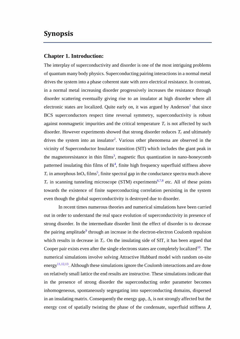
revealed through transmission electron microscopy (TEM) images17. Fig.1 (a) and (d)
show high resolution TEM images probed at the interface of MgO substrate and NbN
film along <110> direction for the two samples with Tc = 16K and 2.5K respectively.
Synopsis 23
The difference between the two films becomes prominent when we take high
resolution scanning TEM data (HRSTEM) as shown in Fig. 1. Panels (b) and (e) shows
HRSTEM image for the two samples with Tc = 16K and 2.5K and panels (c) and (f)
show corresponding two dimensional intensity distribution plots. Intensity in the
HRSTEM image is primarily contributed by Nb and is proportional to the number of
Nb atoms in the probing column. Smooth intensity variation in clean sample (Tc = 16K)
shows the overall thickness variation produced during ion beam milling while the
disordered sample (Tc = 2.5K) shows random distribution of intensity in the columns
showing random number of Nb atoms in the adjacent columns. This clearly shows that
for the disordered films, the lattice contains Nb vacancies but when probed at the large
scale it is homogeneous. Thus we have an ideal system in which disorder is present at
the atomic length scale and the disorder is homogeneous over entire film.
All the work presented in this thesis on disordered NbN is primarily carried out
in our home built STM. Details of the STM and measurement techniques are discussed
in the next chapter.
TC=
2.5
K
d
a
2.44
1
3.87
fe
1.5
2cb
1T
C=
16
K
Figure 1 TEM images (a), (d) High resolution TEM images for samples with Tc = 16K and
2.5K respectively. (b), (e) corresponding high resolution scanning TEM images. (c), (f)
surface plots of 2 dimensional intensity distributions corresponding to (b) and (e)
respectively.
24 Synopsis
Chapter 2. Scanning tunneling microscope
Scanning tunneling microscope (STM) is a powerful tool to probe the electronic
structure of the material at the atomic scale. It works on the principle of quantum
mechanical tunneling between two electrodes through vacuum as a barrier. Essential
parts consist of a sharp metallic tip which is brought near the sample using positioning
units. Small bias applied between tip and sample make the tunneling current flow
between them which is amplified and recorded. Tunneling current exponentially
depends on the distance between tip and sample. By keeping the current constant,
distance between the tip and sample is held constant using feedback loop and by
scanning over the sample the topographic image of the sample is generated.
2.1 Setup
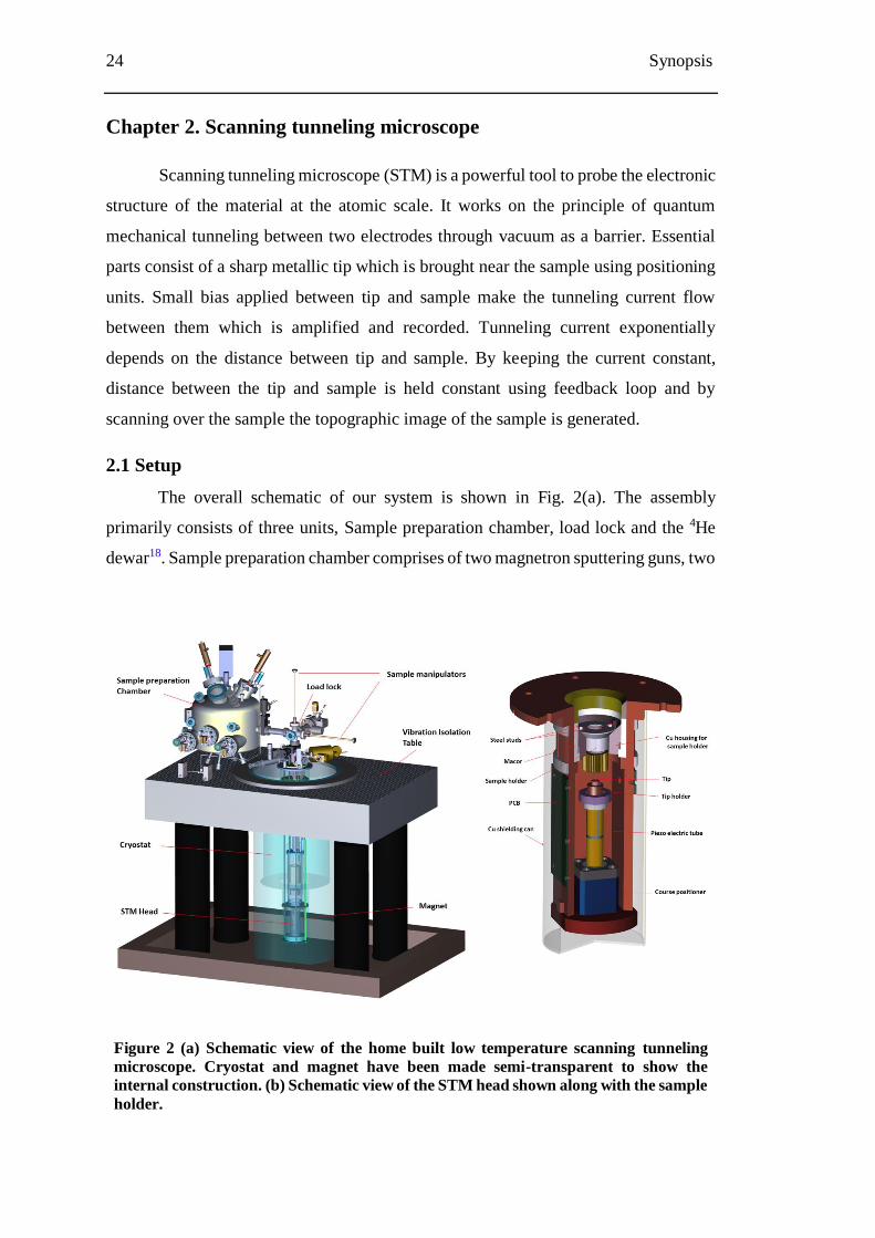
The overall schematic of our system is shown in Fig. 2(a). The assembly
primarily consists of three units, Sample preparation chamber, load lock and the 4He
dewar18. Sample preparation chamber comprises of two magnetron sputtering guns, two
Figure 2 (a) Schematic view of the home built low temperature scanning tunneling
microscope. Cryostat and magnet have been made semi-transparent to show the
internal construction. (b) Schematic view of the STM head shown along with the sample
holder.
Synopsis 25
evaporation sources, a plasma ion etching gun and a heater to heat the sample during
the deposition. Load lock chamber serves as the stage to transfer sample from
deposition chamber into the STM chamber using a pair of transfer manipulators. 4He
dewar has a 9T magnet which houses 3He insert. Helium cryostat hangs from custom
designed vibration isolation table mounted on pneumatic legs and consists of variable
temperature insert (VTI) and STM head. STM head (Fig. 2(b)) attached to the VTI
consists of sample housing assembly, positioning unit and printed circuit board for the
electrical connections. A combination of active and passive vibration isolation systems
are used to obtain the required mechanical stability of the tip. The entire system
operates in a high vacuum of 10-7 mbar and the base temperature for the measurements
is 350mK. Commercially bought control electronics and data acquisition unit (R9,
RHK Technology) is used carry out our experiments.
2.2 Methods
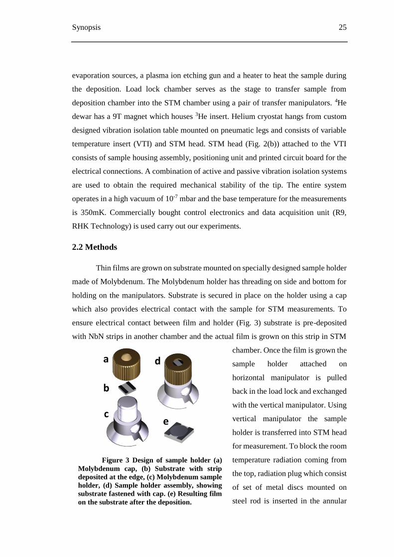
Thin films are grown on substrate mounted on specially designed sample holder
made of Molybdenum. The Molybdenum holder has threading on side and bottom for
holding on the manipulators. Substrate is secured in place on the holder using a cap
which also provides electrical contact with the sample for STM measurements. To
ensure electrical contact between film and holder (Fig. 3) substrate is pre-deposited
with NbN strips in another chamber and the actual film is grown on this strip in STM
chamber. Once the film is grown the
sample holder attached on
horizontal manipulator is pulled
back in the load lock and exchanged
with the vertical manipulator. Using
vertical manipulator the sample
holder is transferred into STM head
for measurement. To block the room
temperature radiation coming from
the top, radiation plug which consist
of set of metal discs mounted on
steel rod is inserted in the annular
Figure 3 Design of sample holder (a)
Molybdenum cap, (b) Substrate with strip
deposited at the edge, (c) Molybdenum sample
holder, (d) Sample holder assembly, showing
substrate fastened with cap. (e) Resulting film
on the substrate after the deposition.
26 Synopsis
region of VTI. Once all the measurements are completed on the sample it is taken out
from the STM and resistivity versus temperature is measured in different cryostat.
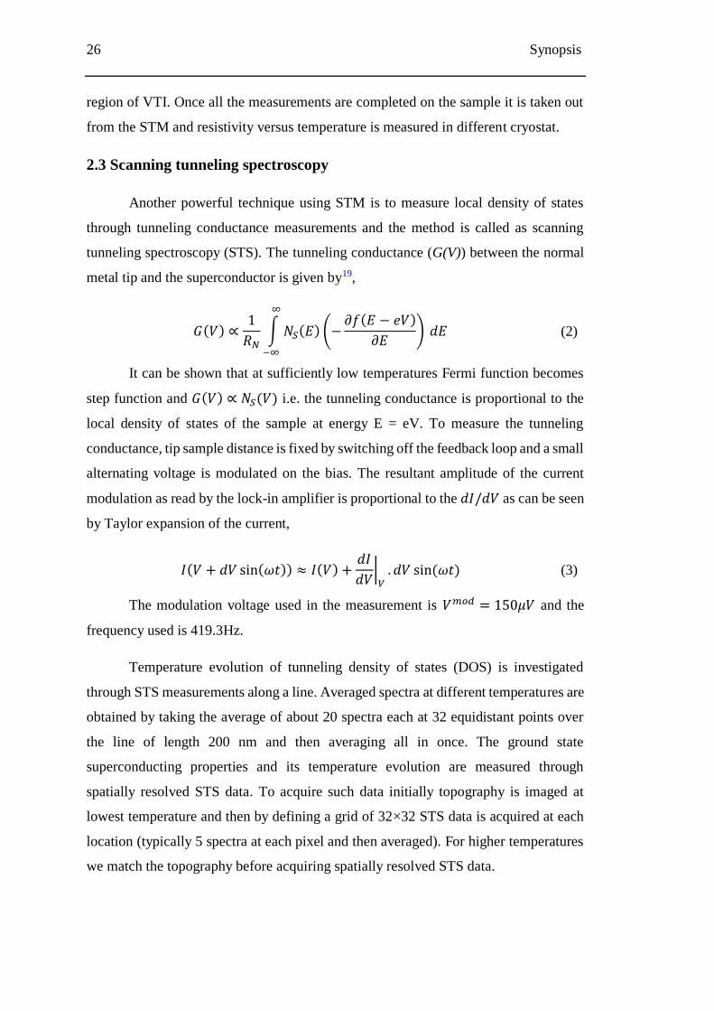
2.3 Scanning tunneling spectroscopy
Another powerful technique using STM is to measure local density of states
through tunneling conductance measurements and the method is called as scanning
tunneling spectroscopy (STS). The tunneling conductance (G(V)) between the normal
metal tip and the superconductor is given by19,
𝐺(𝑉) ∝1
𝑅𝑁∫ 𝑁𝑆(𝐸) (−
𝜕𝑓(𝐸 − 𝑒𝑉)
𝜕𝐸)
∞
−∞
𝑑𝐸 (2)
It can be shown that at sufficiently low temperatures Fermi function becomes
step function and 𝐺(𝑉) ∝ 𝑁𝑆(𝑉) i.e. the tunneling conductance is proportional to the
local density of states of the sample at energy E = eV. To measure the tunneling
conductance, tip sample distance is fixed by switching off the feedback loop and a small
alternating voltage is modulated on the bias. The resultant amplitude of the current
modulation as read by the lock-in amplifier is proportional to the 𝑑𝐼/𝑑𝑉 as can be seen
by Taylor expansion of the current,
𝐼(𝑉 + 𝑑𝑉 sin(𝜔𝑡)) ≈ 𝐼(𝑉) +𝑑𝐼
𝑑𝑉|𝑉. 𝑑𝑉 sin(𝜔𝑡) (3)
The modulation voltage used in the measurement is 𝑉𝑚𝑜𝑑 = 150𝜇𝑉 and the
frequency used is 419.3Hz.
Temperature evolution of tunneling density of states (DOS) is investigated
through STS measurements along a line. Averaged spectra at different temperatures are
obtained by taking the average of about 20 spectra each at 32 equidistant points over
the line of length 200 nm and then averaging all in once. The ground state
superconducting properties and its temperature evolution are measured through
spatially resolved STS data. To acquire such data initially topography is imaged at
lowest temperature and then by defining a grid of 32×32 STS data is acquired at each
location (typically 5 spectra at each pixel and then averaged). For higher temperatures
we match the topography before acquiring spatially resolved STS data.
Synopsis 27
Chapter 3. Emergence of Pseudogap State in Strongly Disordered
NbN
One of the most curious and debated state is the pseudogap state observed in
high Tc superconductors where finite gap in the DOS at Fermi level is observed much
above the superconducting transition temperature which evolves continuously from the
superconducting energy gap below Tc. Several scenarios based either on peculiarities
specific to High Tc Cuprates such as an order competing with superconductivity, or a
superconducting transition driven by phase fluctuations have been suggested as
possible origin of this feature. In this section we elucidate formation of pseudogap state
in NbN using scanning tunneling spectroscopy.
In strong disorder limit all the samples show two distinct features in tunneling
spectra: A low bias dip close to Fermi level which is associated with superconductivity
and a weakly temperature dependent V-shaped background which extends up to high
bias. This second feature which persists up to the highest temperature of our
measurements arises from the Altshuler-Aronov (A-A) type e-e interactions in the
normal state20. To extract the superconducting information from this data we divide the
low temperature spectra by the spectra at sufficiently high temperature where we do
not have any soft gap due to superconducting correlations. The temperature up to which
the pseudogap persists is defined as T*.
-3 -2 -1 0 1 2 3
0.7
0.8
0.9
1.0
4.4K
4.04K
3.61K
3.3K
3.1K
2.6K
G(V
)/G
N
V (mV)
a)
-3 -2 -1 0 1 2 30.7
0.8
0.9
1.0c)
4.04K
3.61K
3.3K
3.1K
2.6K
8K
7K
6.28K
5.33K
4.84K
4.4K
G(V
)/G
N
V (mV)
b)
3 4 5 6 7 8-3.0
-1.5
0.0
1.5
3.0
T*
V (
mV
)
T (K)
1.0
0.8
0.9
G(V
)/G
N
d)
-3 -2 -1 0 1 2 3
-100
0
100
3.1K
3.3K
3.61K
4.04K
5.33K
7K
9.35K
9.35K
8K
7K
6.28K
5.33K
4.84K
dG
(V)/
dv
V (mV)
Figure 4 (a) Normalized conductance curves for the sample with Tc=2.6K.
(b) Derivatives of the conductance curves in panel (a). Few curves are
removed for clarity. (c) Normalized conductance curves after dividing
curves in panel (a) from 9.35K data. (d) Surface plot of the curves of panel
(c)
28 Synopsis
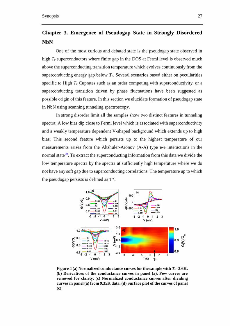
Representative data for one of the strongly disordered samples (Tc = 2.6K) is
shown in Fig. 4. Fig. 4(a) shows conductance spectra at different temperatures. We
observe that the low bias gap feature disappears above 8K and the spectrum at 9.35K
has only the broad background. This is clearly seen in the dG(V)/dV versus V curves
(Fig. 4(b)) where the symmetric peak-dip structure associated with the low bias feature
completely disappears for the spectrum at 9.35K. Therefore to remove the A-A
background from the low temperature spectra we divide the spectrum at 9.35K. Fig.4(c)
shows the divided spectra and Fig. 4 (d) shows the colormap of divided data with x-
axis as the temperature, y-axis as the bias and the colorscale as the normalized
conductance value. The data in panel (d) shows that the pseudogap persists up to 6.5K
i.e. T* = 6.5K.
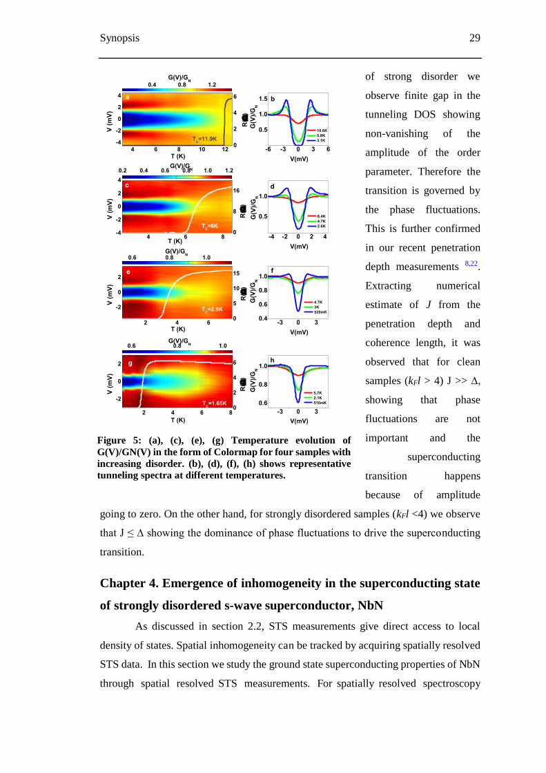
Series of NbN films with increasing disorder were studied using STS. Fig. 5
shows the temperature evolution of tunneling DOS for four samples with Tc = 11.9K,
6K, 2.9K and 1.65K in the form of colormap. All the plots in this figure are corrected
for Altshuler-Aronov background. R-T data for the same sample is indicated by thick
line on top of each colormap. Representative spectra at three temperatures are shown
to the right for clarity. Panel (a) Tc = 11.9K, shows that at low temperature spectra
consist of dip close to zero bias and two symmetric peaks consistent with BCS density
of states. The gap in the spectra vanishes exactly at Tc in accordance with BCS theory
and flat metallic DOS is restored for T > Tc. For the sample with Tc = 6K the gap
remains finite upto slightly higher temperature. For strongly disordered samples (Tc =
2.9K and 1.65K) the gap in the electronic spectra at the Fermi level persists all the way
upto ~7K showing that it forms the pseudogap state and the corresponding T*~ 7K.
Thus we observe that in presence of weak disorder gap closes exactly at Tc while for
strong disorder NbN forms a pseudogapped state above Tc.
Observation of pseudogapped state can be explained using phase fluctuation
scenario. Superconducting order is characterized by complex order parameter given by
Δ0eiφ, where Δ0 is amplitude of the order parameter (which is proportional to the
superconducting energy gap) and φ is the phase, which is same for the entire sample in
the superconducting state. The loss of superconductivity can be because of either
vanishing of this amplitude as described by mean field theories like BCS, or because
of phase fluctuations21 which render φ random. Therefore the superconducting
transition is governed by either ∆ or J, depending on whichever is lower. In presence
Synopsis 29
of strong disorder we
observe finite gap in the
tunneling DOS showing
non-vanishing of the
amplitude of the order
parameter. Therefore the
transition is governed by
the phase fluctuations.
This is further confirmed
in our recent penetration
depth measurements 8,22.
Extracting numerical
estimate of J from the
penetration depth and
coherence length, it was
observed that for clean
samples (kFl > 4) J >> ∆,
showing that phase
fluctuations are not
important and the
superconducting
transition happens
because of amplitude
going to zero. On the other hand, for strongly disordered samples (kFl <4) we observe
that J ≤ ∆ showing the dominance of phase fluctuations to drive the superconducting
transition.
Chapter 4. Emergence of inhomogeneity in the superconducting state
of strongly disordered s-wave superconductor, NbN
As discussed in section 2.2, STS measurements give direct access to local
density of states. Spatial inhomogeneity can be tracked by acquiring spatially resolved
STS data. In this section we study the ground state superconducting properties of NbN
through spatial resolved STS measurements. For spatially resolved spectroscopy
4 6 8 10 12
-4
-2
0
2
4
TC=2.9K
V (
mV
)
T (K)
R(
)
0
2
4
6
0.4 0.8 1.2
G(V)/GN
G(V)/GN
G(V)/GN
G(V)/GN
-6 -3 0 3 6
0.5
1.0
1.5
10.6K
5.8K
3.1K
G(V
)/G
N
V(mV)
4 6 8-4
-2
0
2
4c
V (
mV
)
T (K)
R(
)
TC=6K
0
8
16
0.2 0.4 0.6 0.8 1.0 1.2
-4 -2 0 2 4
0.5
1.0
b
6.4K
4.7K
2.6K
G(V
)/G
N
V(mV)
TC=11.9K
2 4 6
-2
0
2e
V (
mV
)
T (K)
R(
)
0
5
10
15
0.6 0.8 1.0
-3 0 30.4
0.6
0.8
1.0f
4.7K
3K
520mK
G(V
)/G
N
V(mV)
2 4 6 8
-2
0
2
d
g
TC=1.65K
V (
mV
)
T (K)
R(
)
0
2
4
6
0.6 0.8 1.0
-3 0 3
0.6
0.8
1.0h
5.7K
2.1K
510mK
G(V
)/G
N
V(mV)
a
Figure 5: (a), (c), (e), (g) Temperature evolution of
G(V)/GN(V) in the form of Colormap for four samples with
increasing disorder. (b), (d), (f), (h) shows representative
tunneling spectra at different temperatures.
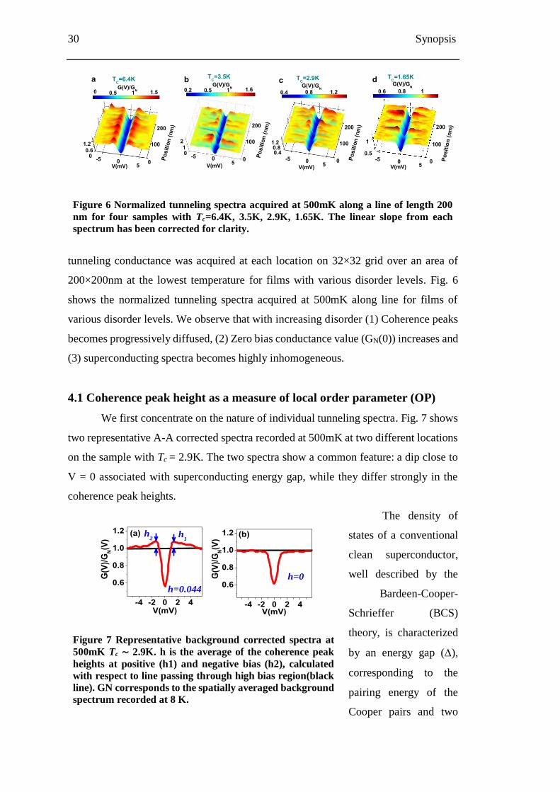
30 Synopsis
tunneling conductance was acquired at each location on 32×32 grid over an area of
200×200nm at the lowest temperature for films with various disorder levels. Fig. 6
shows the normalized tunneling spectra acquired at 500mK along line for films of
various disorder levels. We observe that with increasing disorder (1) Coherence peaks
becomes progressively diffused, (2) Zero bias conductance value (GN(0)) increases and
(3) superconducting spectra becomes highly inhomogeneous.
4.1 Coherence peak height as a measure of local order parameter (OP)
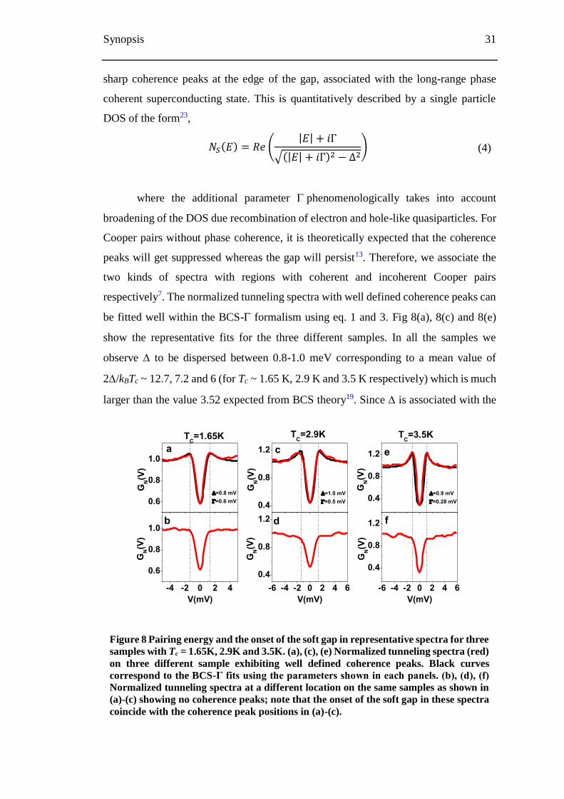
We first concentrate on the nature of individual tunneling spectra. Fig. 7 shows
two representative A-A corrected spectra recorded at 500mK at two different locations
on the sample with Tc = 2.9K. The two spectra show a common feature: a dip close to
V = 0 associated with superconducting energy gap, while they differ strongly in the
coherence peak heights.
The density of
states of a conventional
clean superconductor,
well described by the
Bardeen-Cooper-
Schrieffer (BCS)
theory, is characterized
by an energy gap (),
corresponding to the
pairing energy of the
Cooper pairs and two
b
dc
V(mV)V(mV)V(mV)
0 0
0.6 0.8 1
0.5-5
5
200
100
G(V)/GN
Po
sit
ion
(n
m)
Po
sit
ion
(n
m)
Po
sit
ion
(n
m)
G(V)/GN
G(V)/GN
0
100
200
0
100
200
0-55
0-55
1
0.4 1.20.81.60.5 1
12
0.4
1.20.8
a
0
0.2
TC=1.65KT
C=2.9KT
C=3.5K
0 0.5G(V)/G
N
V(mV)0 0
-55
200
100
Po
sit
ion
(n
m)
1.51
0.61.2
0
TC=6.4K
Figure 6 Normalized tunneling spectra acquired at 500mK along a line of length 200
nm for four samples with Tc=6.4K, 3.5K, 2.9K, 1.65K. The linear slope from each
spectrum has been corrected for clarity.
-4 -2 0 2 4
0.6
0.8
1.0
1.2
-4 -2 0 2 4
0.6
0.8
1.0
1.2h1
G(V
)/G
N(V
)
V(mV)
h=0.044
h2
(a) (b)
h=0
V(mV)
G(V
)/G
N(V
)
Figure 7 Representative background corrected spectra at
500mK Tc ∼ 2.9K. h is the average of the coherence peak
heights at positive (h1) and negative bias (h2), calculated
with respect to line passing through high bias region(black
line). GN corresponds to the spatially averaged background
spectrum recorded at 8 K.
Synopsis 31
sharp coherence peaks at the edge of the gap, associated with the long-range phase
coherent superconducting state. This is quantitatively described by a single particle
DOS of the form23,
𝑁𝑆(𝐸) = 𝑅𝑒 (|𝐸| + 𝑖Γ
√(|𝐸| + 𝑖Γ)2 − Δ2) (4)
where the additional parameter phenomenologically takes into account
broadening of the DOS due recombination of electron and hole-like quasiparticles. For
Cooper pairs without phase coherence, it is theoretically expected that the coherence
peaks will get suppressed whereas the gap will persist13. Therefore, we associate the
two kinds of spectra with regions with coherent and incoherent Cooper pairs
respectively7. The normalized tunneling spectra with well defined coherence peaks can
be fitted well within the BCS- formalism using eq. 1 and 3. Fig 8(a), 8(c) and 8(e)
show the representative fits for the three different samples. In all the samples we
observe to be dispersed between 0.8-1.0 meV corresponding to a mean value of
2/kBTc ~ 12.7, 7.2 and 6 (for Tc ~ 1.65 K, 2.9 K and 3.5 K respectively) which is much
larger than the value 3.52 expected from BCS theory19. Since is associated with the
0.6
0.8
1.0
-4 -2 0 2 4
0.6
0.8
1.0
0.4
0.8
1.2
-6 -4 -2 0 2 4 6
0.4
0.8
1.2
0.4
0.8
1.2
-6 -4 -2 0 2 4 6
0.4
0.8
1.2 f
e
db
c
TC=3.5KT
C=2.9K
=0.8 mV
=0.6 mV
GN(V
)
TC=1.65K
a
GN(V
)
V(mV)
=1.0 mV
=0.5 mV
GN(V
)
GN(V
)
V(mV)
=0.9 mV
=0.28 mV
GN(V
)
GN(V
)
V(mV)
Figure 8 Pairing energy and the onset of the soft gap in representative spectra for three
samples with Tc = 1.65K, 2.9K and 3.5K. (a), (c), (e) Normalized tunneling spectra (red)
on three different sample exhibiting well defined coherence peaks. Black curves
correspond to the BCS-Γ fits using the parameters shown in each panels. (b), (d), (f)
Normalized tunneling spectra at a different location on the same samples as shown in
(a)-(c) showing no coherence peaks; note that the onset of the soft gap in these spectra
coincide with the coherence peak positions in (a)-(c).
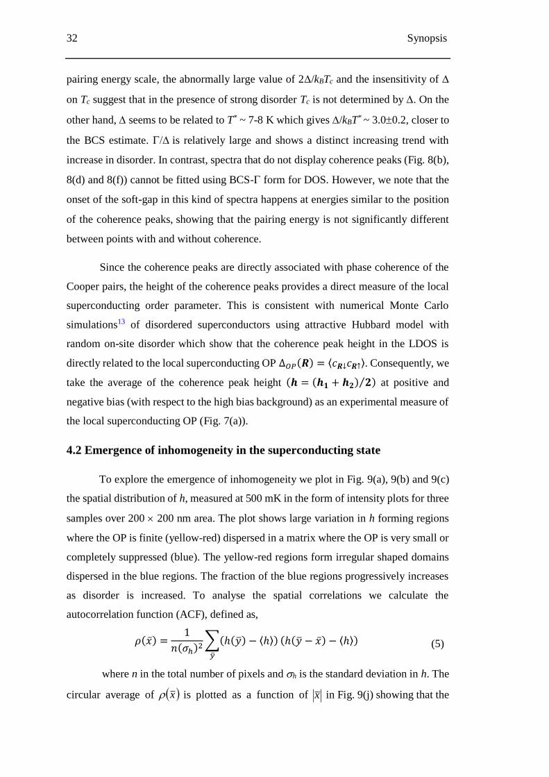
32 Synopsis
pairing energy scale, the abnormally large value of 2/kBTc and the insensitivity of
on Tc suggest that in the presence of strong disorder Tc is not determined by . On the
other hand, seems to be related to T* ~ 7-8 K which gives /kBT* ~ 3.00.2, closer to
the BCS estimate. is relatively large and shows a distinct increasing trend with
increase in disorder. In contrast, spectra that do not display coherence peaks (Fig. 8(b),
8(d) and 8(f)) cannot be fitted using BCS- form for DOS. However, we note that the
onset of the soft-gap in this kind of spectra happens at energies similar to the position
of the coherence peaks,showing that the pairing energy is not significantly different
between points with and without coherence.
Since the coherence peaks are directly associated with phase coherence of the
Cooper pairs, the height of the coherence peaks provides a direct measure of the local
superconducting order parameter. This is consistent with numerical Monte Carlo
simulations13 of disordered superconductors using attractive Hubbard model with
random on-site disorder which show that the coherence peak height in the LDOS is
directly related to the local superconducting OP Δ𝑂𝑃(𝑹) = ⟨𝑐𝑹↓𝑐𝑹↑⟩. Consequently, we
take the average of the coherence peak height (𝒉 = (𝒉𝟏 + 𝒉𝟐) 𝟐⁄ ) at positive and
negative bias (with respect to the high bias background) as an experimental measure of
the local superconducting OP (Fig. 7(a)).
4.2 Emergence of inhomogeneity in the superconducting state
To explore the emergence of inhomogeneity we plot in Fig. 9(a), 9(b) and 9(c)
the spatial distribution of h, measured at 500 mK in the form of intensity plots for three
samples over 200 200 nm area. The plot shows large variation in h forming regions
where the OP is finite (yellow-red) dispersed in a matrix where the OP is very small or
completely suppressed (blue). The yellow-red regions form irregular shaped domains
dispersed in the blue regions. The fraction of the blue regions progressively increases
as disorder is increased. To analyse the spatial correlations we calculate the
autocorrelation function (ACF), defined as,
𝜌(�̅�) =1
𝑛(𝜎ℎ)2∑(ℎ(�̅�) − ⟨ℎ⟩)
�̅�
(ℎ(�̅� − �̅�) − ⟨ℎ⟩) (5)
where n in the total number of pixels and h is the standard deviation in h. The
circular average of x is plotted as a function of x in Fig. 9(j) showing that the
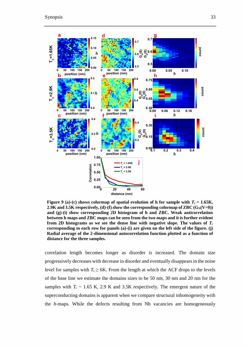
Synopsis 33
correlation length becomes longer as disorder is increased. The domain size
progressively decreases with decrease in disorder and eventually disappears in the noise
level for samples with Tc ≥ 6K. From the length at which the ACF drops to the levels
of the base line we estimate the domains sizes to be 50 nm, 30 nm and 20 nm for the
samples with Tc ~ 1.65 K, 2.9 K and 3.5K respectively. The emergent nature of the
superconducting domains is apparent when we compare structural inhomogeneity with
the h-maps. While the defects resulting from Nb vacancies are homogeneously
0 50 100 150 2000.00
0.05
0.10
0.15
0 50 100 150 200
0.5
0.6
0.7
0.00 0.05 0.10
0.5
0.6
0.7
0 50 100 150 2000.0
0.1
0.2
0 50 100 150 200
0.4
0.6
0.8
0.00 0.06 0.12 0.180.30
0.45
0.60
0.75
0 50 100 150 2000.0
0.2
0.4
0 50 100 150 200
0.2
0.4
0.1 0.2 0.3 0.40.00
0.15
0.30
0 20 40 600.00
0.25
0.50
0.75
1.00
position (nm)
position (nm)
GN(0
)
h
GN(0
)
co
un
t
position (nm)
i
h
g
f
e
d
c
b
position (nm)
GN(0
)
a
h
GN(0
)
co
un
t
position (nm)
h
position (nm)
GN(0
)
TC=
3.5
KT
C=
2.9
K
h
h
h
GN(0
)
co
un
t
TC=
1.6
5K
Tc = 1.65K
Tc = 2.9K
Tc = 3.5K
j
distance (nm)
Co
rre
lati
on
Figure 9 (a)-(c) shows colormap of spatial evolution of h for sample with Tc = 1.65K,
2.9K and 3.5K respectively, (d)-(f) show the corresponding colormap of ZBC (GN(V=0))
and (g)-(i) show corresponding 2D histogram of h and ZBC. Weak anticorrelation
between h maps and ZBC maps can be seen from the two maps and it is further evident
from 2D histograms as we see the dense line with negative slope. The values of Tc
corresponding to each row for panels (a)-(i) are given on the left side of the figure. (j)
Radial average of the 2-dimensional autocorrelation function plotted as a function of
distance for the three samples.
34 Synopsis
distributed over atomic length scales, the domains formed by superconducting
correlations over this disordered landscape is 2 orders of magnitude larger.
The domain patterns observed in h-maps is also visible in Fig. 9(d), 9(e)
and 9(f) when we plot the maps of zero bias conductance (ZBC), GN(0), for the same
samples. The ZBC maps show an inverse correlation with the h-maps: Regions where
the superconducting OP is large have a smaller ZBC than places where the OP is
suppressed. The cross-correlation between the h-map and ZBC map can be computed
through the cross-correlator defined as,
𝐼 =1
𝑛∑
(ℎ(𝑖, 𝑗) − ⟨ℎ⟩)(𝑍𝐵𝐶(𝑖, 𝑗) − ⟨𝑍𝐵𝐶⟩)
𝜎ℎ𝜎𝑍𝐵𝐶𝑖,𝑗
(6)
where n is the total number of pixels and ZBC is the standard deviations in the
values of ZBC. A perfect correlation (anti-correlation) between the two images would
correspond to I = 1(-1). We obtain a cross correlation, I ≈ -0.3 showing that the anti-
correlation is weak. Thus ZBC is possibly not governed by the local OP alone. This is
also apparent in the 2-dimensional histograms of h and ZBC (Fig. 9(g), 9(h) and 9(i))
which show a large scatter over a negative slope.
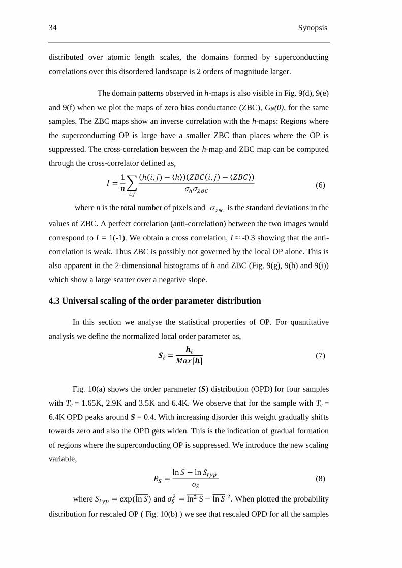
4.3 Universal scaling of the order parameter distribution
In this section we analyse the statistical properties of OP. For quantitative
analysis we define the normalized local order parameter as,
𝑺𝒊 =𝒉𝒊
𝑀𝑎𝑥[𝒉] (7)
Fig. 10(a) shows the order parameter (S) distribution (OPD) for four samples
with Tc = 1.65K, 2.9K and 3.5K and 6.4K. We observe that for the sample with Tc =
6.4K OPD peaks around S = 0.4. With increasing disorder this weight gradually shifts
towards zero and also the OPD gets widen. This is the indication of gradual formation
of regions where the superconducting OP is suppressed. We introduce the new scaling
variable,
𝑅𝑆 =ln𝑆 − ln 𝑆𝑡𝑦𝑝
𝜎𝑆 (8)
where 𝑆𝑡𝑦𝑝 = exp (ln 𝑆̅̅ ̅̅ ̅) and 𝜎𝑆2 = ln2 S̅̅ ̅̅ ̅̅ − ln 𝑆̅̅ ̅̅ ̅ 2. When plotted the probability
distribution for rescaled OP ( Fig. 10(b) ) we see that rescaled OPD for all the samples
Synopsis 35
collapse onto a single curve showing
universality of the OPD The OPD is
also in good agreement with Tracy-
Widom distribution whose relevance
is recently discussed in connection
with directed polymer physics in
finite dimensions24,25. We also
identify similar scaling relation of the
OPD within two prototype fermionic
and bosonic models for disordered
superconductors26 showing an
excellent agreement between
experiment and theory. Agreement
between theory and experiments also
confirms the correct identification of
the local OP.
4.4 Temperature evolution of the inhomogeneous superconducting state in
NbN
In this section we will focus on temperature evolution of domain structure that
is seen at the lowest temperature as the system is driven across Tc into pseudogap state.
At high temperatures coherence peaks get diffused due to thermal broadening and the
h-maps can no longer be used as a reliable measure of the OP distribution. This problem
is however overcome by tracking the zero bias conductance (ZBC) value in the
tunneling spectra to track temperature evolution of domains based on our observation
of weak anticorrelation between h maps and ZBC maps at lowest temperature.
We investigated the temperature evolution of the domains as a function of
temperature for the sample with Tc ~ 2.9 K. The bulk pseudogap temperature was first
determined for this sample by measuring the tunneling spectra at 64 points along a 200
nm line at ten different temperatures. Fig.11(a) shows the temperature evolution of the
normalized tunneling spectra along with temperature variation of resistance. In
0.0 0.2 0.4 0.6 0.80
1
2
3
4 6.4K
3.5K
2.9K
1.65K
S
P(S)
-4 -2 0 20.0
0.2
0.4
0.6
6.4K
3.5K
2.9K
1.65K
TW
RS
P (
RS
)
a
b
Figure 10 (a) Order parameter
distribution for the four samples (b) The
same data as in panel (a) plotted in terms of
the rescaled variable RS. The solid line
corresponds to the Tracy-Widom
distribution.
36 Synopsis
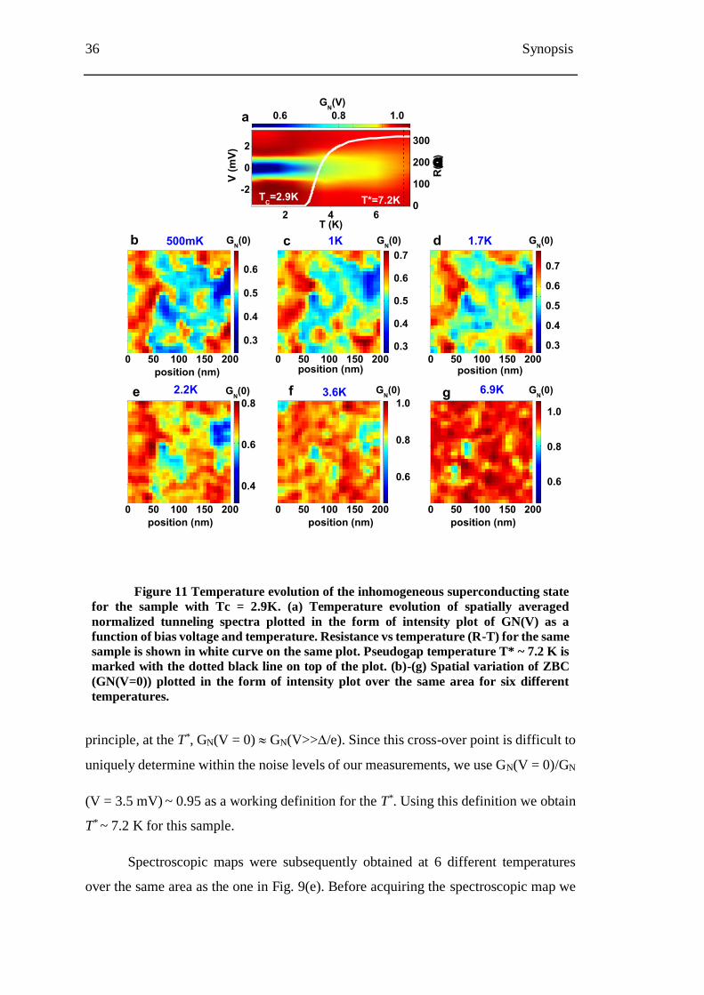
principle, at the T*, GN(V = 0) GN(V>>/e). Since this cross-over point is difficult to
uniquely determine within the noise levels of our measurements, we use GN(V = 0)/GN
(V = 3.5 mV) ~ 0.95 as a working definition for the T*. Using this definition we obtain
T* ~ 7.2 K for this sample.
Spectroscopic maps were subsequently obtained at 6 different temperatures
over the same area as the one in Fig. 9(e). Before acquiring the spectroscopic map we
0 50 100 150 200
0.3
0.4
0.5
0.6
0 50 100 150 200
0.3
0.4
0.5
0.6
0.7
0 50 100 150 200
0.3
0.4
0.5
0.6
0.7
0 50 100 150 200
0.4
0.6
0.8
0 50 100 150 200
0.6
0.8
1.0
0 50 100 150 200
0.6
0.8
1.0
GN(0)G
N(0)G
N(0)
GN(0)G
N(0)c
position (nm)
GN(0)
a
position (nm)
position (nm)
position (nm)
b
position (nm)
6.9K3.6K2.2K
1.7K1K
gfe
d
position (nm)
500mK
2 4 6
-2
0
2
T*=7.2KTC=2.9K
a)
V (
mV
)T (K)
R(
)
0
100
200
300
0.6 0.8 1.0
GN(V)
Figure 11 Temperature evolution of the inhomogeneous superconducting state
for the sample with Tc = 2.9K. (a) Temperature evolution of spatially averaged
normalized tunneling spectra plotted in the form of intensity plot of GN(V) as a
function of bias voltage and temperature. Resistance vs temperature (R-T) for the same
sample is shown in white curve on the same plot. Pseudogap temperature T* ~ 7.2 K is
marked with the dotted black line on top of the plot. (b)-(g) Spatial variation of ZBC
(GN(V=0)) plotted in the form of intensity plot over the same area for six different
temperatures.
Synopsis 37
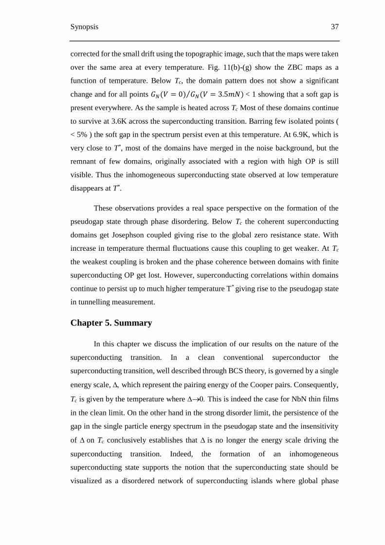
corrected for the small drift using the topographic image, such that the maps were taken
over the same area at every temperature. Fig. 11(b)-(g) show the ZBC maps as a
function of temperature. Below Tc, the domain pattern does not show a significant
change and for all points 𝐺𝑁(𝑉 = 0) 𝐺𝑁(𝑉 = 3.5𝑚𝑁)⁄ < 1 showing that a soft gap is
present everywhere. As the sample is heated across Tc Most of these domains continue
to survive at 3.6K across the superconducting transition. Barring few isolated points (
< 5% ) the soft gap in the spectrum persist even at this temperature. At 6.9K, which is
very close to T*, most of the domains have merged in the noise background, but the
remnant of few domains, originally associated with a region with high OP is still
visible. Thus the inhomogeneous superconducting state observed at low temperature
disappears at T*.
These observations provides a real space perspective on the formation of the
pseudogap state through phase disordering. Below Tc the coherent superconducting
domains get Josephson coupled giving rise to the global zero resistance state. With
increase in temperature thermal fluctuations cause this coupling to get weaker. At Tc
the weakest coupling is broken and the phase coherence between domains with finite
superconducting OP get lost. However, superconducting correlations within domains
continue to persist up to much higher temperature T* giving rise to the pseudogap state
in tunnelling measurement.
Chapter 5. Summary
In this chapter we discuss the implication of our results on the nature of the
superconducting transition. In a clean conventional superconductor the
superconducting transition, well described through BCS theory, is governed by a single
energy scale, which represent the pairing energy of the Cooper pairs. Consequently,
Tc is given by the temperature where This is indeed the case for NbN thin films
in the clean limit. On the other hand in the strong disorder limit, the persistence of the
gap in the single particle energy spectrum in the pseudogap state and the insensitivity
of on Tc conclusively establishes that is no longer the energy scale driving the
superconducting transition. Indeed, the formation of an inhomogeneous
superconducting state supports the notion that the superconducting state should be
visualized as a disordered network of superconducting islands where global phase
38 Synopsis
coherence is established below Tc through Josephson tunneling between
superconducting islands. Consequently at Tc, the phase coherence would get destroyed
through thermal phase fluctuations between the superconducting domains, while
coherent and incoherent Cooper pairs would continue to survive as evidenced from the
persistence of the domain structure and the soft gap in the tunneling spectrum at
temperatures above Tc. Finally, at T* we reach the energy scale set by the pairing energy
where the domain structure and the soft gap disappears.
These measurements connect naturally to direct measurements of the superfluid
phase stiffness (J) performed through low frequency penetration depth and high
frequency complex conductivity ( 'i” ) measurements on similar NbN
samples. Low frequency measurements8 reveal that in the same range of disorder where
the pseudogap appears ( Tc ≤ 6K), J(T 0) becomes a lower energy scale compared to
High frequency microwave measurements27 reveal that in the pseudogap regime
the superfluid stiffness becomes strongly frequency dependent. While at low
frequencies J ( ”) becomes zero close to Tc showing that the global phase
coherent state is destroyed, at higher frequencies J continues to remain finite up to a
higher temperature, which coincides with T* in the limit of very high frequencies. Since
at the probing length scale set by the electron diffusion length at microwave
frequencies27 is of the same order as the size of the domains observed in STS, finite J
at these frequencies implies that the phase stiffness continues to remains finite within
the individual phase coherent domains. Similar results were also obtained from the
microwave complex conductivity of strongly disordered InOx thin films28.
In summary, we have demonstrated the emergence of an inhomogeneous
superconducting state, consisting of domains made of phase coherent and incoherent
Cooper pairs in homogeneously disordered NbN thin films. The domains are observed
both in the local variation of coherence peak heights as well as in the ZBC which show
a weak inverse correlation with respect to each other. The origin of a finite ZBC at low
temperatures as well as this inverse correlation is not understood at present and should
form the basis for future theoretical investigations close to the SIT. However, the
persistence of these domains above Tc and subsequent disappearance only close to T*
provide a real space perspective on the nature of the superconducting transition, which
is expected to happen through thermal phase fluctuations between the phase coherent
Synopsis 39
domains, even when the pairing interaction remains finite. However, an understanding
of the explicit connection between this inhomogeneous state and percolative transport
for the temperature above and below Tc is currently incomplete29,30,31 and its
formulation would further enrich our understanding of the superconducting transition
in strongly disordered superconductors.
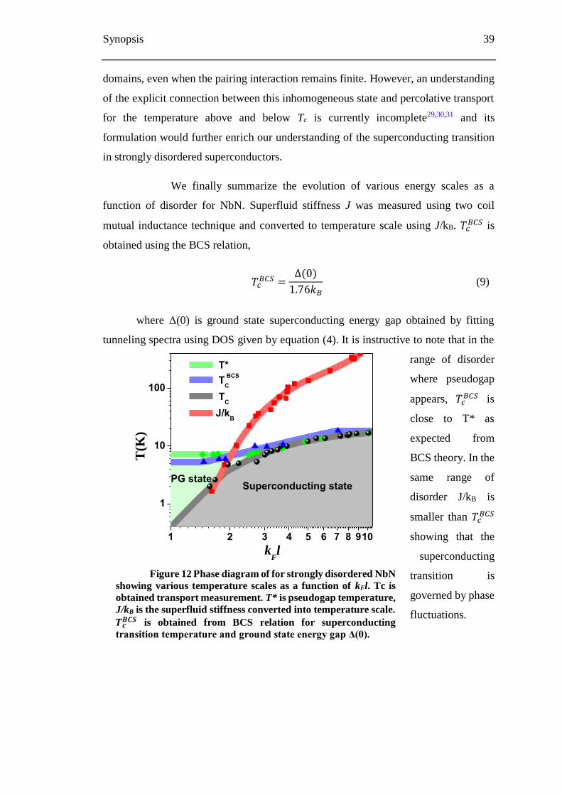
We finally summarize the evolution of various energy scales as a
function of disorder for NbN. Superfluid stiffness J was measured using two coil
mutual inductance technique and converted to temperature scale using J/kB. 𝑇𝑐𝐵𝐶𝑆 is
obtained using the BCS relation,
𝑇𝑐𝐵𝐶𝑆 =
∆(0)
1.76𝑘𝐵 (9)
where Δ(0) is ground state superconducting energy gap obtained by fitting
tunneling spectra using DOS given by equation (4). It is instructive to note that in the
range of disorder
where pseudogap
appears, 𝑇𝑐𝐵𝐶𝑆 is
close to T* as
expected from
BCS theory. In the
same range of
disorder J/kB is
smaller than 𝑇𝑐𝐵𝐶𝑆
showing that the
superconducting
transition is
governed by phase
fluctuations.
1 2 3 4 5 6 7 8 910
1
10
100
PG state
T(K
)
kFl
T*
T BCS
C
TC
J/kB
Superconducting state
Figure 12 Phase diagram of for strongly disordered NbN
showing various temperature scales as a function of kFl. Tc is
obtained transport measurement. T* is pseudogap temperature,
J/kB is the superfluid stiffness converted into temperature scale.
𝑻𝒄𝑩𝑪𝑺 is obtained from BCS relation for superconducting
transition temperature and ground state energy gap Δ(0).
40 Synopsis
References
1 P W Anderson,
J. Phys. Chem. Solids 11 26 (1959)
2 A. M. Goldman and N Markovic
Phys. Today 51 39 (1998)
3 Sambandamurthy G et al, Phys. Rev. Lett. 94 017003 (2005); Baturina T I et
al, Phys. Rev. Lett, 98 127003 (2007); Nguyen H Q et al, Phys. Rev. Lett.
103 157001 (2009)
4 M. D. Stewart Jr., A. Yin, J. M. Xu, and J. M. Valles Jr.
Science 318 1273 (2007)
5 R. Crane, N. P. Armitage, A. Johansson, G. Sambandamurthy, D. Shahar, and
G. Grüner
Phys. Rev. B 75 184530 (2007)
6 B. Sacépé, C. Chapelier, T. I. Baturina, V. M. Vinokur, M. R. Baklanov, and
M. Sanquer
Nat. Comm. 1 140 (2010)
7 B. Sacépé, T. Dubouchet, C. Chapelier, M. Sanquer, M. Ovadia, D. Shahar,
M. Feigel'man, and L. Ioffe
Nat. Phys. 7 239 (2011)
8 M. Mondal, A. Kamlapure, M. Chand, G. Saraswat, S. Kumar, J. Jesudasan,
L. Benfatto, V. Tripathi, and P. Raychaudhuri
Phys. Rev. Lett. 106 047001 (2011)
9 P. W. Anderson et al, Phys. Rev. B 28 117 (1983); A. M. Finkelstein, Phys. B
197 636 (1994)
10 M, Ma and P. Lee,
Phys. Rev. B 32 5658 (1985)
11 A. Ghosal, M. Randeria, and N. Trivedi
Phys. Rev. Lett. 81 3940 (1998)
12 Y. Dubi, Y. Meir and Y. Avishai
Nature, 449 876 (2007)
13 K. Bouadim, Y. L. Loh, M. Randeria, and N. Trivedi
Synopsis 41
Nat. Phys. 7 884 (2011)
14 M. Mondal, M. Chand, A. Kamlapure, J. Jesudasan, V. C. Bagwe, S. Kumar,
G. Saraswat, V. Tripathi and P. Raychaudhuri, J. Supercond. Nov. Magn. 24
341 (2011)
15 S. P. Chockalingam, Madhavi Chand, John Jesudasan, Vikram Tripathi and
Pratap Raychaudhuri
Phys. Rev. B 77, 214503 (2008)
16 M. Chand, A. Mishra, Y. M. Xiong, A. Kamlapure, S. P. Chockalingam, J.
Jesudasan, V. Bagwe, M. Mondal, P. W. Adams, V. Tripathi, and P.
Raychaudhuri
Phys. Rev. B 80, 134514 (2009)
17 A. Kamlapure, T. Das, S. C. Ganguli, J. B Parmar, S. Bhattacharyya, P.
Raychaudhuri
arxiv.org/abs/1308.2880 (2013)
18 A. Kamlapure, G. Saraswat, S.C. Ganguli, V. Bagwe, P. Raychaudhuri, S. P
Pai
arxiv.org/abs/1308.4496 (2013)
19 Tinkham, M Introduction to Superconductivity (Dover Publications Inc.,
Mineola, New York, 2004).
20 B. L. Altshuler and A. G. Aronov
Phys. Rev. Lett. 44 1288 (1980).
21 V. J. Emery and S. A. Kivelson,
Phys. Rev. Lett. 74 3253 (1995).
22 M. Chand, G. Saraswat, A. Kamlapure, M. Mondal, S. Kumar, J. Jesudasan,
V. Bagwe, L. Benfatto, V. Tripathi, and P. Raychaudhuri
Phys. Rev. B 85, 014508 (2012)
23 Dynes, R. C., Narayanamurti, V., and Garno, J. P. Direct Measurement of
Quasiparticle-Lifetime Broadening in a Strong-Coupled Superconductor. Phys.
Rev. Lett. 41, 1509 (1978).
24 C. Monthus and T. Garel, J. Stat. Mech.: Theory Exp. P01008 (2012)
25 C. Monthus and T. Garel, J. Phys. A: Math. Theor. 45, 095002 (2012).
26 G. Lemarié, A. Kamlapure, D. Bucheli, L. Benfatto, J. Lorenzana, G. Seibold,
S. C. Ganguli, P. Raychaudhuri and C. Castellani
42 Synopsis
Phys. Rev. B 85 184509 (2013)
27 M. Mondal, A. Kamlapure, S. C. Ganguli, J. Jesudasan, V. Bagwe, L.
Benfatto and P. Raychaudhuri.
Scientific Reports 3, 1357 (2013).
28 Liu, W., Kim, M., Sambandamurthy, G. and Armitage, N. P.
Phys. Rev. B 84, 024511(2011).
29 Bucheli, D., Caprara, S., Castellani, C. and Grilli, M.
New Journal of Physics 15, 023014 (2013).
30 Li, Y., Vicente, C. L. and Yoon, J.
Phys. Rev. B 81, 020505(R) (2010).
31 Seibold, G., Benfatto, L., Castellani, C. & Lorenzana, J.
Phys. Rev. Lett. 108, 207004 (2012).
Chapter 1
Introduction
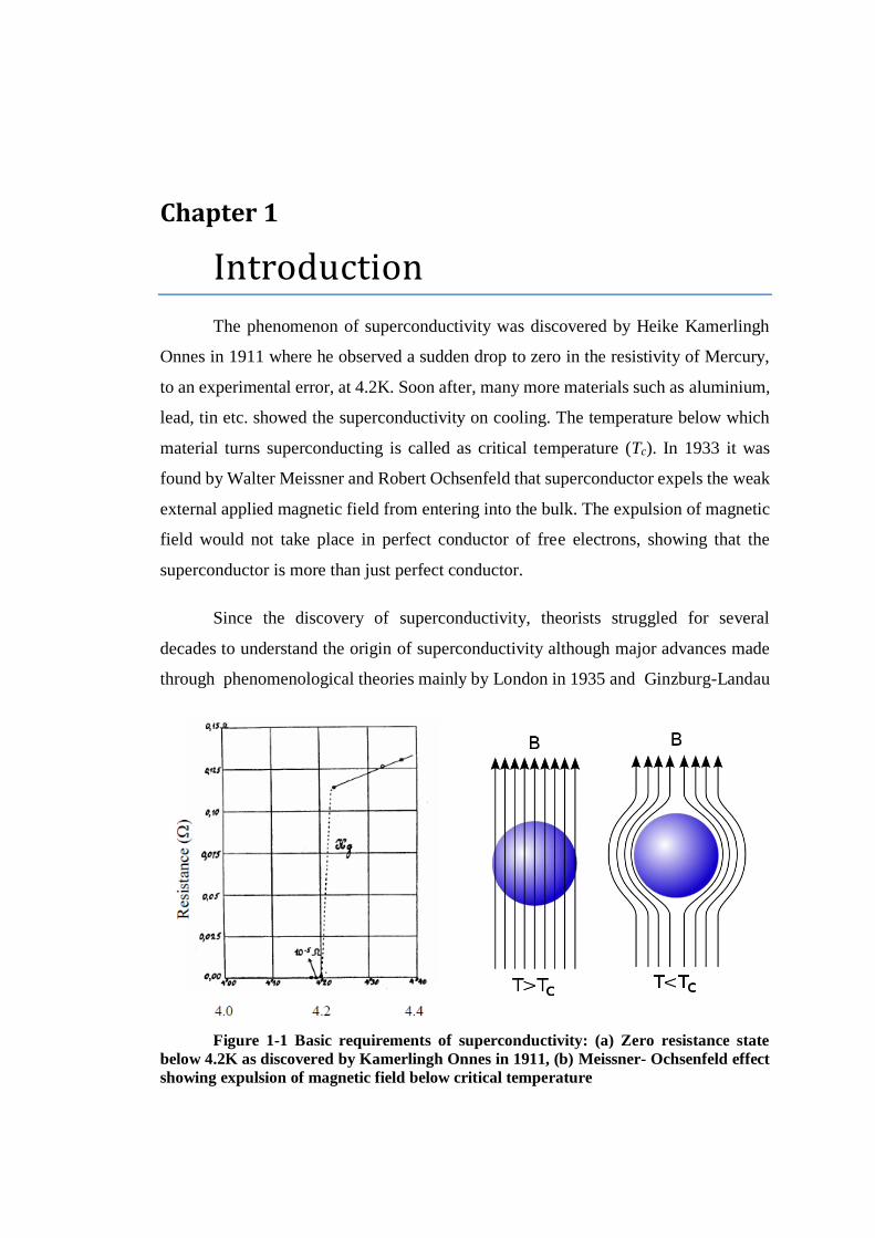
The phenomenon of superconductivity was discovered by Heike Kamerlingh
Onnes in 1911 where he observed a sudden drop to zero in the resistivity of Mercury,
to an experimental error, at 4.2K. Soon after, many more materials such as aluminium,
lead, tin etc. showed the superconductivity on cooling. The temperature below which
material turns superconducting is called as critical temperature (Tc). In 1933 it was
found by Walter Meissner and Robert Ochsenfeld that superconductor expels the weak
external applied magnetic field from entering into the bulk. The expulsion of magnetic
field would not take place in perfect conductor of free electrons, showing that the
superconductor is more than just perfect conductor.
Since the discovery of superconductivity, theorists struggled for several
decades to understand the origin of superconductivity although major advances made
through phenomenological theories mainly by London in 1935 and Ginzburg-Landau
Figure 1-1 Basic requirements of superconductivity: (a) Zero resistance state
below 4.2K as discovered by Kamerlingh Onnes in 1911, (b) Meissner- Ochsenfeld effect
showing expulsion of magnetic field below critical temperature
44 Chapter 1. Introduction
in 1950. It is John Bardeen, Leon Neil Cooper, and John Robert Schrieffer (BCS) who
first gave the microscopic theory of superconductivity in 1957. The basic idea in the
BCS theory is that in the superconducting state electrons pair though phonon coupling
and these pairs, called as Cooper pairs, condense into a single phase coherent ground
state which allows the electrons to move without scattering.
For the obvious technological reasons search for the new materials which could
superconduct at higher temperatures continued and in 1986 Alex Müller and Karl
Bednorz discovered a new class of superconductor known as the doped rare earth
cuprates. These materials become superconducting above 30K. In following years a
host of new material were found which superconduct at temperatures much higher than
the boiling point of liquid N2. These new class of materials are called as high
temperature superconductors (HTSC). Not much progress is made in understanding the
origin of HTSC although there are theories which qualitatively explain the possible
mechanism of pairing and symmetry of the gap.
While the quest for new materials continued, there have been also the
investigations by some researchers on the effect of disorder on superconducting
properties of the material. The problem gives a unique opportunity to study the
competition between superconductivity which results from pairing and the pair
breaking effects of electron localization and disorder induced Coulomb repulsion. The
interest in the field was further increased by the possibility that the disorder driven or
magnetic field driven suppression of superconductivity in the limit of zero temperature
might be a quantum phase transition.
In this thesis we study the effect of disorder on superconducting properties of
s-wave superconductor, NbN, close to metal insulator transition. The study was mainly
carried out using home built low temperature Scanning Tunneling Microscopes (STM).
The plan of the introduction chapter is as follows. In the first section I will describe the
basics of superconductivity and essential concept required to make platform for our
study. I will then review the experimental and theoretical advances in the field of
disorder/ magnetic field driven superconductor insulator transition (SIT). I will finally
introduce to our model system NbN and its characterization through transport
measurements and transmission electron microscopy (TEM).
Chapter 1. Introduction 45
1.1 Basics of Superconductivity
1.1.A The Meissner-Ochsenfeld effect
When a superconductor is cooled below its Tc and kept in a weak external
magnetic field then it expels the magnetic flux lines from entering into the bulk so that
the field inside a superconductor is zero (B = 0). This phenomenon is called as
Meissner-Ochsenfeld effect. Although superconductors show the perfect diamagnetism
at low fields, strong magnetic fields destroy the superconductivity. The field at which
superconductivity breaks down is called as the critical field (Bc)
1.1.B The London equations
The phenomenological theory developed by London brothers1 in 1935 explains
the perfect conductivity as well as the Meissner effect where they showed that the
superconductor produces screening current at the surface which shields the external
magnetic field from entering into the bulk. The two equation governing electromagnetic
fields inside a superconductor are,
𝜕𝒋𝒔𝜕𝑡=𝑒2𝑛𝑠𝑚
𝑬 (1.1)
∇ × 𝐣𝒔 = −
𝑒2𝑛𝑠𝑚𝑐
𝑩 (1.2)
The first equation essentially explains the perfect conductivity through the free
acceleration of charge. Using the identities in vector calculus and Amperes law one can
deduce the second equation to,
∇2𝑩 =1
𝜆𝐿2𝑩 (1.3)
Where 𝜆𝐿 is called as London penetration depth and is defined as,
𝜆𝐿 = √𝑚𝑐2
4𝜋𝑒2𝑛𝑠 (1.4)
One can immediately see that on application of magnetic field 𝑩 = 𝐵𝑎𝑝𝑙�̂� to
semi-infinite superconductor (Figure 1-2), the magnetic field inside the superconductor
is given by
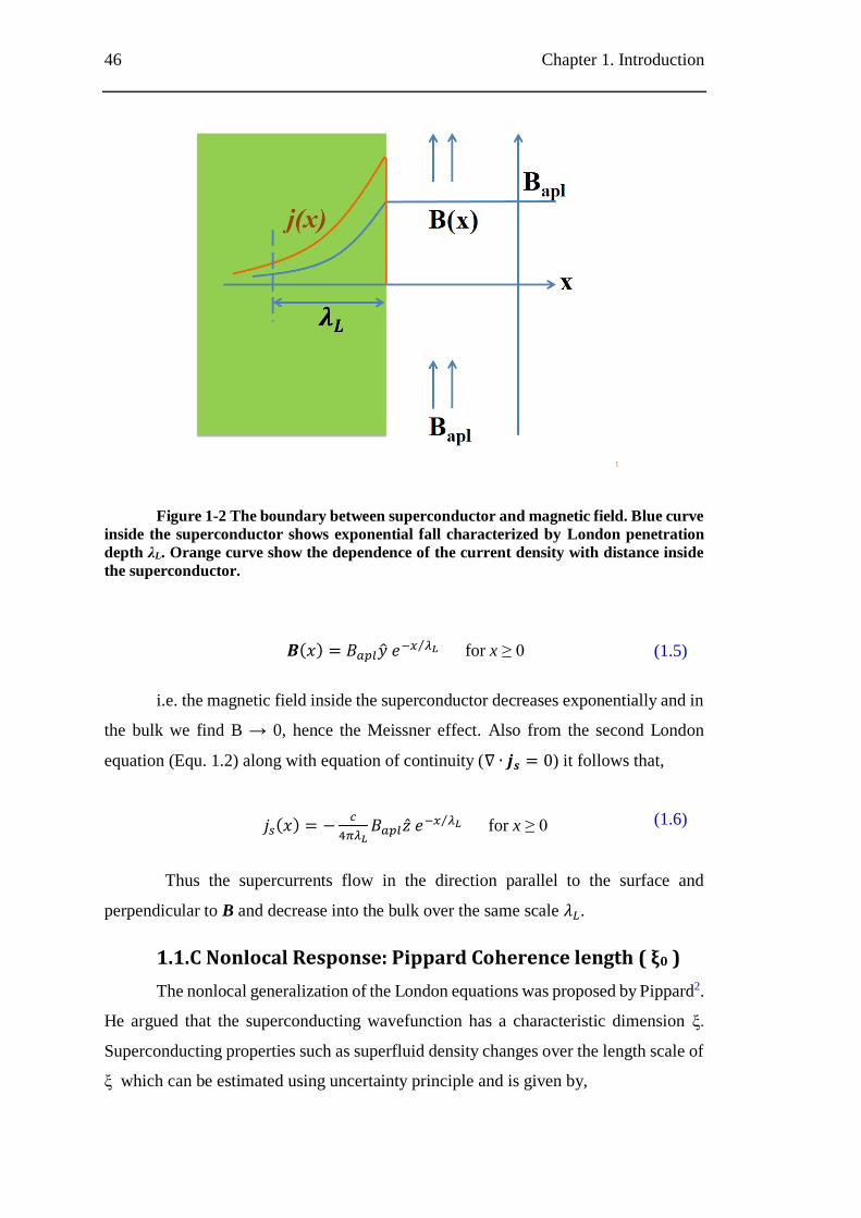
46 Chapter 1. Introduction
Figure 1-2 The boundary between superconductor and magnetic field. Blue curve
inside the superconductor shows exponential fall characterized by London penetration
depth λL. Orange curve show the dependence of the current density with distance inside
the superconductor.
𝑩(𝑥) = 𝐵𝑎𝑝𝑙�̂� 𝑒−𝑥 𝜆𝐿⁄ for x ≥ 0 (1.5)
i.e. the magnetic field inside the superconductor decreases exponentially and in
the bulk we find B → 0, hence the Meissner effect. Also from the second London
equation (Equ. 1.2) along with equation of continuity (∇ ∙ 𝒋𝒔 = 0) it follows that,
𝑗𝑠(𝑥) = −𝑐
4𝜋𝜆𝐿𝐵𝑎𝑝𝑙�̂� 𝑒
−𝑥 𝜆𝐿⁄ for x ≥ 0 (1.6)
Thus the supercurrents flow in the direction parallel to the surface and
perpendicular to B and decrease into the bulk over the same scale 𝜆𝐿.
1.1.C Nonlocal Response: Pippard Coherence length ( ξ0 )
The nonlocal generalization of the London equations was proposed by Pippard2.
He argued that the superconducting wavefunction has a characteristic dimension ξ.
Superconducting properties such as superfluid density changes over the length scale of
ξ which can be estimated using uncertainty principle and is given by,
Chapter 1. Introduction 47
ξ = 𝛼ℏ𝑣𝐹𝑘𝐵𝑇𝑐
(1.7)
Where α is a numeric constant of the order of unity. BCS theory predicts that
the value of α ≈ 0.18. It also has a physical significance in BCS theory that it represents
the size of the Cooper pairs.
1.1.D Ginzburg Landau (G-L) model of superconductivity
The phenomenological theory of superconductivity was introduced by
Ginzburg and Landau3 in 1950 which describes superconducting phase transition
within Landau’s general theory of second order phase transition. They introduced a
complex pseudo-wave function 𝜓 = |𝜓|𝑒𝑖𝜑 as an order parameter to describe
superconducting electrons.
G-L equation can be obtained using the variational principle to minimize the
free energy and it has the form analogous to Schrodinger’s equation,
1
2𝑚∗(ℏ
𝑖∇ −
𝑒∗
𝑐𝑨)
2
𝜓 + 𝛽|𝜓|2𝜓 = −𝛼(𝑇)𝜓 (1.8)
The corresponding equation for supercurrent is,
𝑱𝒔 =𝑒∗ℏ
𝑖2𝑚∗(𝜓∗∇𝜓 − 𝜓∇𝜓∗) −
𝑒∗2
𝑚∗𝑐|𝜓|2𝑨 (1.9)
With 𝜓 = |𝜓|𝑒𝑖𝜑 and using equ. 1.8 we can get the equation for supercurrent
velocity as,
𝒗𝒔 =ℏ
2𝑚(∇𝜑 −
2𝑒
ℏ𝑐𝑨) (1.10)
It can be shown that G-L order parameter can be related to local density of
superelectrons as,
𝑛𝑠∗ = |𝜓(𝑥)|2 = −
𝛼
𝛽 (1.11)
48 Chapter 1. Introduction
Phase stiffness
Bulk superconducting ground state is described by a constant order parameter,
𝜓, where the phase of the order parameter, 𝜑, has a constant value everywhere. There
is an energy cost associated with changing 𝜑 from one part of the superconductor to
another. This energy cost is called as phase stiffness or superfluid stiffness and denoted
as J. From equ. 1.10, the velocity of the superfluid is given by,
𝑣𝑠 =ℏ
2𝑚(∇φ) (1.12)
Now the increase in kinetic energy by phase twist is given by
𝑛𝑠 ∫ 𝑑3𝑟 (
1
2𝑚𝑣𝑠
2) =1
2
ℏ2𝑛𝑠
4𝑚∫𝑑3𝑟(∇𝜑)2. In analogy with XY model4,5 in statistical
physics we define J over the cut-off distance 𝑎 as6,7,
𝐽 =ℏ2𝑛𝑠𝑎
4𝑚 (1.13)
For all our analysis we take the minimum cut-off distance a equal to coherence
length ξ as it is a characteristic length scale over which the superconducting parameters
changes. It is important to note that 𝐽 ∝ 𝑛𝑠 which is related to λL (equ. 1.4) which is
experimentally measureable quantity.
G-L Characteristic length scales
Solving G-L equation at the interface of superconductor introduces a
characteristic length called as G-L coherence length given by 𝜉 = (ℏ2
2𝑚∗|𝛼(𝑇)|)1 2⁄
and it
is the measure of the distance over which order parameter respond to a perturbation.
To the first order approximation in α, it can be written as, 𝜉(𝑇) = 𝜉(0)|𝑡|−1 2⁄ , where
𝑡 =𝑇𝑐−𝑇
𝑇𝑐.
Also the London penetration depth can be written as,
𝜆 = √𝑚𝑐2
4𝜋𝑒2𝑛𝑠= √
𝑚𝑐2
8𝜋𝑒2 (−𝛼𝛽) (1.14)
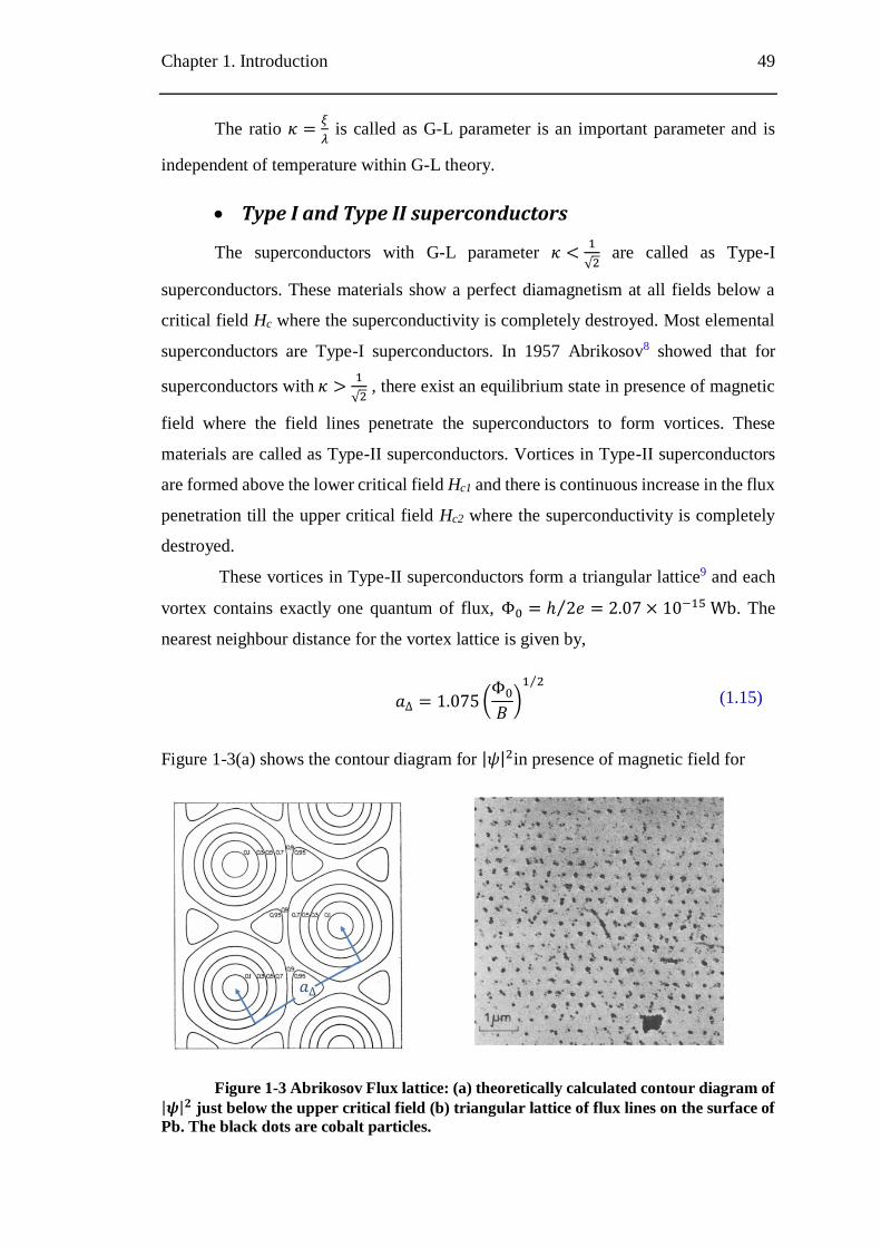
Chapter 1. Introduction 49
The ratio 𝜅 =𝜉
𝜆 is called as G-L parameter is an important parameter and is
independent of temperature within G-L theory.
Type I and Type II superconductors
The superconductors with G-L parameter 𝜅 <1
√2 are called as Type-I
superconductors. These materials show a perfect diamagnetism at all fields below a
critical field Hc where the superconductivity is completely destroyed. Most elemental
superconductors are Type-I superconductors. In 1957 Abrikosov8 showed that for
superconductors with 𝜅 >1
√2 , there exist an equilibrium state in presence of magnetic
field where the field lines penetrate the superconductors to form vortices. These
materials are called as Type-II superconductors. Vortices in Type-II superconductors
are formed above the lower critical field Hc1 and there is continuous increase in the flux
penetration till the upper critical field Hc2 where the superconductivity is completely
destroyed.
These vortices in Type-II superconductors form a triangular lattice9 and each
vortex contains exactly one quantum of flux, Φ0 = ℎ 2𝑒⁄ = 2.07 × 10⁻¹⁵ Wb. The
nearest neighbour distance for the vortex lattice is given by,
𝑎∆ = 1.075 (Φ0𝐵)1 2⁄
(1.15)
Figure 1-3(a) shows the contour diagram for |𝜓|2in presence of magnetic field for
Figure 1-3 Abrikosov Flux lattice: (a) theoretically calculated contour diagram of
|𝝍|𝟐 just below the upper critical field (b) triangular lattice of flux lines on the surface of
Pb. The black dots are cobalt particles.
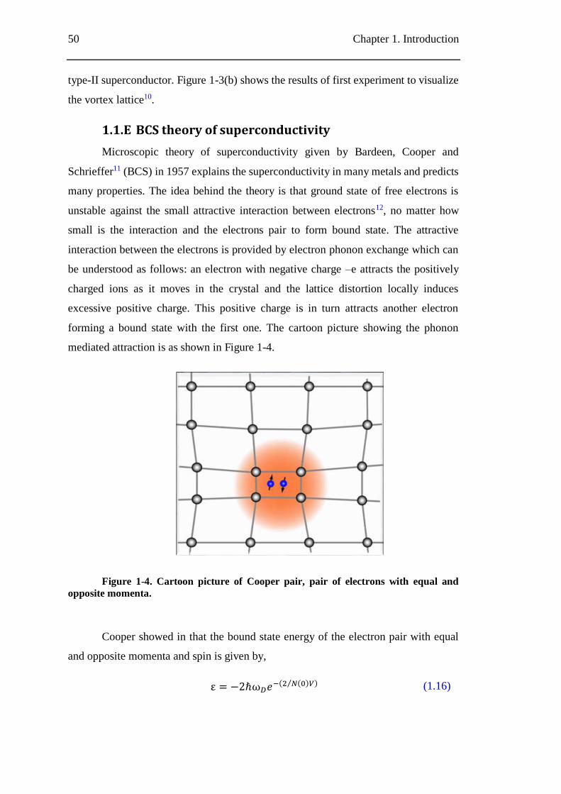
50 Chapter 1. Introduction
type-II superconductor. Figure 1-3(b) shows the results of first experiment to visualize
the vortex lattice10.
1.1.E BCS theory of superconductivity
Microscopic theory of superconductivity given by Bardeen, Cooper and
Schrieffer11 (BCS) in 1957 explains the superconductivity in many metals and predicts
many properties. The idea behind the theory is that ground state of free electrons is
unstable against the small attractive interaction between electrons12, no matter how
small is the interaction and the electrons pair to form bound state. The attractive
interaction between the electrons is provided by electron phonon exchange which can
be understood as follows: an electron with negative charge –e attracts the positively
charged ions as it moves in the crystal and the lattice distortion locally induces
excessive positive charge. This positive charge is in turn attracts another electron
forming a bound state with the first one. The cartoon picture showing the phonon
mediated attraction is as shown in Figure 1-4.
Figure 1-4. Cartoon picture of Cooper pair, pair of electrons with equal and
opposite momenta.
Cooper showed in that the bound state energy of the electron pair with equal
and opposite momenta and spin is given by,
ε = −2ℏω𝐷𝑒−(2 𝑁(0)⁄ 𝑉) (1.16)
Chapter 1. Introduction 51
where 𝜔𝐷is the cut-off frequency corresponding to the Debye temperature. Next
we will briefly review the BCS theory11.
BCS took the form for the ground state as,
|𝜓𝐺⟩ = ∏ (𝑢𝑘 + 𝑣𝑘𝑐𝑘↑+ 𝑐−𝑘↓
+ )|𝜙0⟩
𝑘=𝑘1,…𝑘𝑀
Where |𝑢𝑘|2 + |𝑣𝑘|
2 = 1 and |𝜙0⟩ is the vacuum state. Coefficients 𝑢𝑘 and 𝑢𝑘
are chosen so as to minimize the expectation value of the energy using the so called
reduced Hamiltonian,
ℋ =∑𝜖𝑘𝑛𝑘𝜎𝑘𝜎
+∑𝑉𝑘𝑙𝑐𝑘↑+
𝑘𝑙
𝑐−𝑘↓+ 𝑐−𝑙↓𝑐𝑙↑ (1.17)
BCS assumed the simple form for the attractive interaction 𝑉𝑘𝑙 as,
𝑉𝑘𝑙 = {−𝑉, |ξ𝑘|and |ξ𝑙| ≤ ℏω𝐷0, Otherwise
(1.18)
Where ξ𝑘 is the single particle energy of the electrons with respect to Fermi
energy. Following are the important key results of BCS theory,
The gap function
Δ(0) = 2ℏω𝐷𝑒−1 𝑁(0)⁄ 𝑉 (1.19)
Where Δ is the superconducting energy gap formed at the Fermi level and 𝑁(0)
is Fermi level density of states.
Temperature dependence of the gap and Tc
Temperature dependence of the gap can be numerically calculated using,
1
𝑁(0)𝑉= ∫
tanh12𝛽(𝜉2 + Δ2)1 2⁄
(𝜉2 + Δ2)1 2⁄ 𝑑𝜉
ℏω𝐷
0
(1.20)
where 𝛽 = (𝑘𝐵𝑇)−1. Figure 1-5 shows the temperature dependence of ∆ which
holds in good approximation for most of the conventional superconductors.
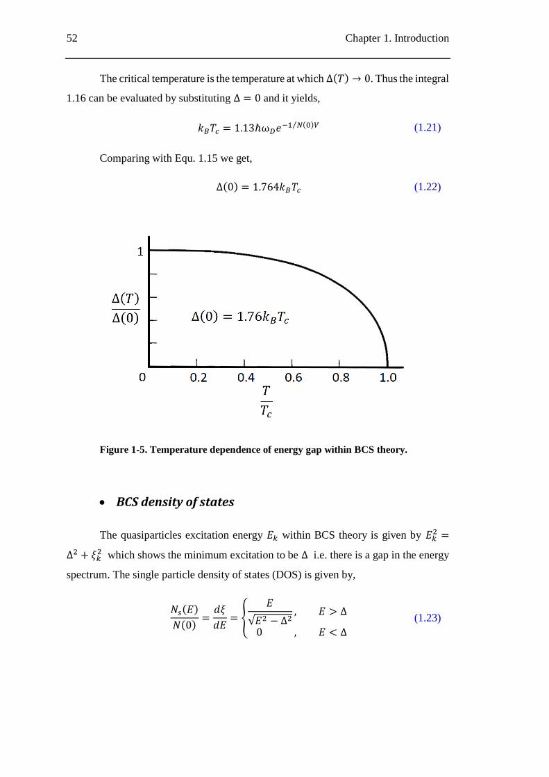
52 Chapter 1. Introduction
The critical temperature is the temperature at which Δ(𝑇) → 0. Thus the integral
1.16 can be evaluated by substituting Δ = 0 and it yields,
𝑘𝐵𝑇𝑐 = 1.13ℏω𝐷𝑒−1 𝑁(0)⁄ 𝑉 (1.21)
Comparing with Equ. 1.15 we get,
Δ(0) = 1.764𝑘𝐵𝑇𝑐 (1.22)
Figure 1-5. Temperature dependence of energy gap within BCS theory.
BCS density of states
The quasiparticles excitation energy 𝐸𝑘 within BCS theory is given by 𝐸𝑘2 =
∆2 + 𝜉𝑘2 which shows the minimum excitation to be ∆ i.e. there is a gap in the energy
spectrum. The single particle density of states (DOS) is given by,
𝑁𝑠(𝐸)
𝑁(0)=𝑑𝜉
𝑑𝐸= {
𝐸
√𝐸2 − Δ2, 𝐸 > Δ
0 , 𝐸 < Δ
(1.23)
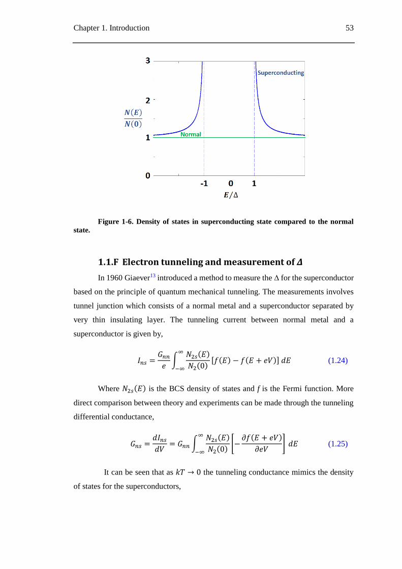
Chapter 1. Introduction 53
Figure 1-6. Density of states in superconducting state compared to the normal
state.
1.1.F Electron tunneling and measurement of ∆
In 1960 Giaever13 introduced a method to measure the ∆ for the superconductor
based on the principle of quantum mechanical tunneling. The measurements involves
tunnel junction which consists of a normal metal and a superconductor separated by
very thin insulating layer. The tunneling current between normal metal and a
superconductor is given by,
𝐼𝑛𝑠 =𝐺𝑛𝑛𝑒∫
𝑁2𝑠(𝐸)
𝑁2(0)[𝑓(𝐸) − 𝑓(𝐸 + 𝑒𝑉)] 𝑑𝐸
∞
−∞
(1.24)
Where 𝑁2𝑠(𝐸) is the BCS density of states and f is the Fermi function. More
direct comparison between theory and experiments can be made through the tunneling
differential conductance,
𝐺𝑛𝑠 =𝑑𝐼𝑛𝑠𝑑𝑉
= 𝐺𝑛𝑛∫𝑁2𝑠(𝐸)
𝑁2(0)[−𝜕𝑓(𝐸 + 𝑒𝑉)
𝜕𝑒𝑉] 𝑑𝐸
∞
−∞
(1.25)
It can be seen that as 𝑘𝑇 → 0 the tunneling conductance mimics the density
of states for the superconductors,
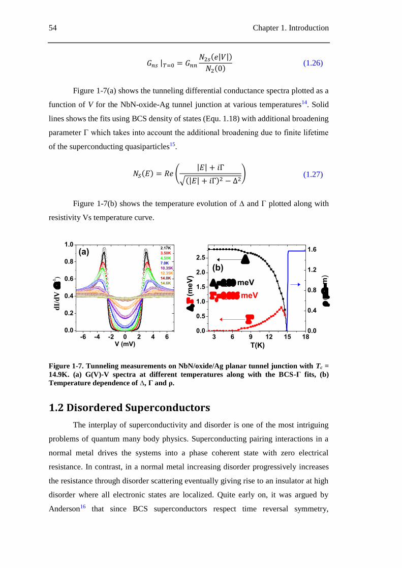
54 Chapter 1. Introduction
𝐺𝑛𝑠 |𝑇=0 = 𝐺𝑛𝑛𝑁2𝑠(𝑒|𝑉|)
𝑁2(0) (1.26)
Figure 1-7(a) shows the tunneling differential conductance spectra plotted as a
function of V for the NbN-oxide-Ag tunnel junction at various temperatures14. Solid
lines shows the fits using BCS density of states (Equ. 1.18) with additional broadening
parameter Γ which takes into account the additional broadening due to finite lifetime
of the superconducting quasiparticles15.
𝑁𝑆(𝐸) = 𝑅𝑒 (|𝐸| + 𝑖Γ
√(|𝐸| + 𝑖Γ)2 − Δ2) (1.27)
Figure 1-7(b) shows the temperature evolution of ∆ and Γ plotted along with
resistivity Vs temperature curve.
3 6 9 12 15 180.0
0.5
1.0
1.5
2.0
2.5
0.0
0.4
0.8
1.2
1.6
-6 -4 -2 0 2 4 60.0
0.2
0.4
0.6
0.8
1.0
m
)
(m
eV
)
T(K)
(a)
meV
meV
dI/
dV
(
-1)
V (mV)
2.17K
3.50K
4.50K
7.0K
10.35K
12.35K
14.0K
14.6K
(b)
Figure 1-7. Tunneling measurements on NbN/oxide/Ag planar tunnel junction with Tc =
14.9K. (a) G(V)-V spectra at different temperatures along with the BCS-Γ fits, (b)
Temperature dependence of ∆, Γ and ρ.
1.2 Disordered Superconductors
The interplay of superconductivity and disorder is one of the most intriguing
problems of quantum many body physics. Superconducting pairing interactions in a
normal metal drives the systems into a phase coherent state with zero electrical
resistance. In contrast, in a normal metal increasing disorder progressively increases
the resistance through disorder scattering eventually giving rise to an insulator at high
disorder where all electronic states are localized. Quite early on, it was argued by
Anderson16 that since BCS superconductors respect time reversal symmetry,
Chapter 1. Introduction 55
superconductivity is robust against nonmagnetic impurities and the critical temperature
Tc is not affected by such disorder. Anderson’s idea however applies only to weakly
disordered systems, with their extended electronic states. In presence of strong disorder
experiments showed that it reduces Tc and ultimately drives the system into an
insulator17,18,19,20. This suppression of superconductivity could be thickness
driven21,22,23, magnetic field driven24 or disorder driven25,26. Various other novel
phenomena are observed in the vicinity of superconductor insulator transition (SIT).
The two key observations are (i) persistence of finite superconducting correlations
above Tc through measurements of finite high J stiffness above Tc in amorphous InOx
films27,28, finite spectral gap at zero bias in the conductance spectra much above Tc in
scanning tunneling microscope (STM) experiments29,30,31 etc., and (ii) presence of
superconducting correlations/ Cooper pairing through the measurements of activated
temperature dependence of resistance on the insulating side32, the giant peak in the
magnetoresistance in thin films33,34,35, magnetic flux quantization in nano-honeycomb
patterned insulating thin films of Bi36, a more recent transport37,38 and tunneling
experiments39.
Although the complete theoretical understanding of the nature of SIT is lacking,
in recent times numerous theoretical and numerical advances have been made. It is
shown that in the intermediate disorder limit the effect of disorder is to decrease the
pairing amplitude40,41 through an increase in the electron-electron (e-e) Coulomb
repulsion which results in decrease in Tc. In presence of strong disorder experimental
observations are understood qualitatively through number of prototype models of
disordered superconductors which are based on either fermionic42,43,44,45,46 or
bosonic47,48,49 description. The fermionic models demonstrated the survival spectral
gap across SIT and the transition is driven by phase fluctuation between
superconducting islands. Bosonic models indicated that the SIT is driven by quantum
phase fluctuations between localized Cooper pairs.
In particular here I would like to highlight on the recent numerical simulations
which have direct relevance to the work presented in this thesis. These simulations
involve solving Attractive (negative-U) Hubbard model with random on-site
energy43,50,45. While these studies ignore Coulomb interactions and are done on
relatively small systems compared to real superconductors, they nevertheless support
56 Chapter 1. Introduction
key aspects of the basic scenario of the disordered superconductors namely (i) Single
particle spectral gap in the DOS at lowest temperature survives through SIT and is finite
everywhere though it is highly inhomogeneous. However J, decreases rapidly with
increasing disorder making the system more susceptible to phase fluctuations. (ii)
Coherence peak heights at the gap edge are directly correlated to the local
superconducting order and vanish with increasing temperature and disorder. (iii) Near
SIT, pseudogap appears in the DOS at low energies above Tc and also on the insulating
side. These results are indeed in good agreement with our results on disordered NbN
presented in this thesis.
In spite of the fact that the field of disordered superconductors has produced
variety of novel phenomena and interesting theoretical results which has enriched our
understanding of SIT to a great extent, more experimental works are needed for
complete understanding and resolving the open questions in the field. More
specifically, in regard of theoretical propositions, suggesting the emergence novel
phenomena beyond the ambit of BCS theory, there is very little direct experimental
evidence confirming the predictions made. In this thesis we address most of the
experimental remedies through our investigation on NbN which can be grown with
larger atomic defects by tweaking growth parameters.
1.3 Our model system: NbN
For our investigation we use NbN as a model system to study the effect of
disorder. NbN is a conventional s-wave superconductor with optimum Tc ~ 17K. Bulk
NbN has the λ of ~ 250 nm, electronic mean free of l ~ 4nm and the ξ ~ 5nm. It has
face centred cubic structure similar to NaCl. Band structure calculations show that
Fermi level lies within the 4d band and these electrons contribute to the conduction.
1.3.A Sample growth and introducing disorder
Epitaxial thin films of NbN are grown using reactive DC magnetron sputtering
in Ar+N2 gas mixture on (100) oriented single crystalline MgO substrate which is
heated to 600°C. The optimum conditions to get the highest Tc of 17K are sputtering
power =200W, Ar:N2 ratio = 84:16. The disorder in the system is tuned by varying
deposition conditions: either by decreasing the sputtering power keeping the partial gas
pressures constant or by increasing the N2 partial pressure51,52. In both these cases Nb
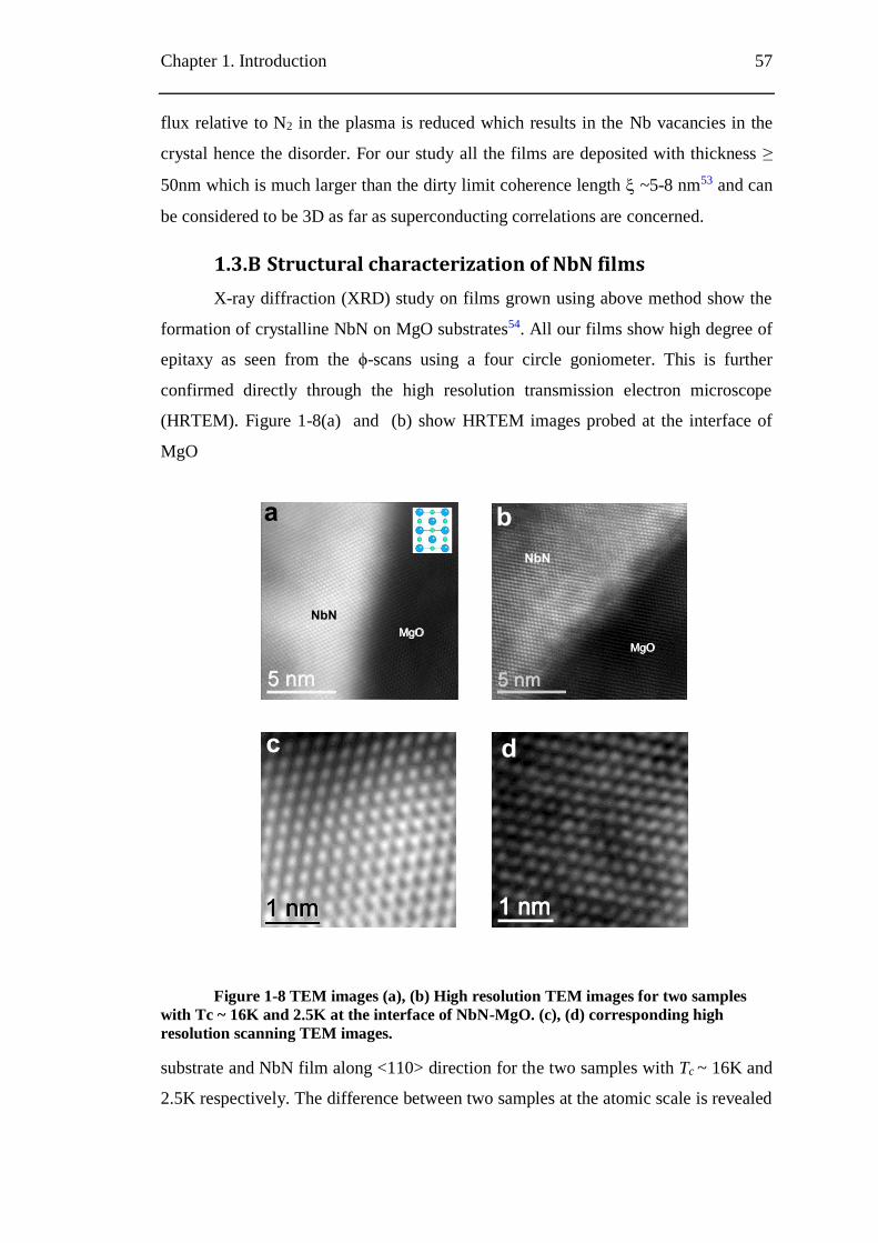
Chapter 1. Introduction 57
flux relative to N2 in the plasma is reduced which results in the Nb vacancies in the
crystal hence the disorder. For our study all the films are deposited with thickness ≥
50nm which is much larger than the dirty limit coherence length ~5-8 nm53 and can
be considered to be 3D as far as superconducting correlations are concerned.
1.3.B Structural characterization of NbN films
X-ray diffraction (XRD) study on films grown using above method show the
formation of crystalline NbN on MgO substrates54. All our films show high degree of
epitaxy as seen from the ϕ-scans using a four circle goniometer. This is further
confirmed directly through the high resolution transmission electron microscope
(HRTEM). Figure 1-8(a) and (b) show HRTEM images probed at the interface of
MgO
1 nm
MgO
MgO
NbN
dc
ba
NbN
1 nm
Figure 1-8 TEM images (a), (b) High resolution TEM images for two samples
with Tc ~ 16K and 2.5K at the interface of NbN-MgO. (c), (d) corresponding high
resolution scanning TEM images.
substrate and NbN film along <110> direction for the two samples with Tc ~ 16K and
2.5K respectively. The difference between two samples at the atomic scale is revealed
58 Chapter 1. Introduction
in Figure 1-8(c) and (d) which shows the high resolution scanning transmission
(HRSTEM) images for same samples respectively. Intensity in the HRSTEM image is
primarily contributed by Nb and is proportional to the number of Nb atoms in the
probing column. Smooth intensity variation in clean sample (Tc ~ 16K) shows the
overall thickness variation produced during ion beam milling while the disordered
sample (Tc ~ 2.5K) shows random distribution of intensity in the columns showing
random number of Nb atoms in the adjacent columns. This clearly shows that for the
disordered films, the lattice contains Nb vacancies but when probed at the large scale
it is homogeneous. Thus we have an ideal system in which disorder is present at the
atomic length scale and the disorder is homogeneous over entire film.
1.3.C Quantification of disorder
To quantify disorder we use the Ioffe Regel parameter 𝑘𝐹𝑙 which is the measure
of mean free path 𝑙 in units of de-Broglie wavelength (𝜆𝐹). In clean system 𝑙 ≫ 𝜆𝐹 and
therefore 𝑘𝐹𝑙 has a large value. With increasing disorder 𝑙 decreases steadily due to
disorder scattering and therefore the quantity 𝑘𝐹𝑙 also decreases. At 𝑘𝐹𝑙 ≤ 1 all the
bloch states are completely localized which corresponds to Anderson metal insulator
transition (MIT). 𝑘𝐹𝑙 values are extracted from resistivity and Hall measurements and
calculated using free electron formula,
𝑘𝐹𝑙 =(3𝜋2)2 3⁄ ℏ[𝑅𝐻(285𝐾)]
1 3⁄
𝜌(285𝐾)𝑒5 3⁄ (1.28)
Here 𝑅𝐻 = −1
𝑛𝑒 assumes absence of e-e interaction which is not the case for
our disordered samples. Therefore we calculate 𝑘𝐹𝑙 at highest temperature of our
measurements (i.e. at 285K) where the effects of interaction is believed to be smaller55.
𝑘𝐹𝑙 in our samples ranges from 10 (Tc = 16K) to all the way down to 0.42 (Tc < 300mK)
and we observe that 𝑘𝐹𝑙 ~ 1 is the critical disorder where superconductivity is
completely destroyed.
1.4 Effects of disorder
In this section we will review our recent work on disordered NbN through the
transport and λ measurements.
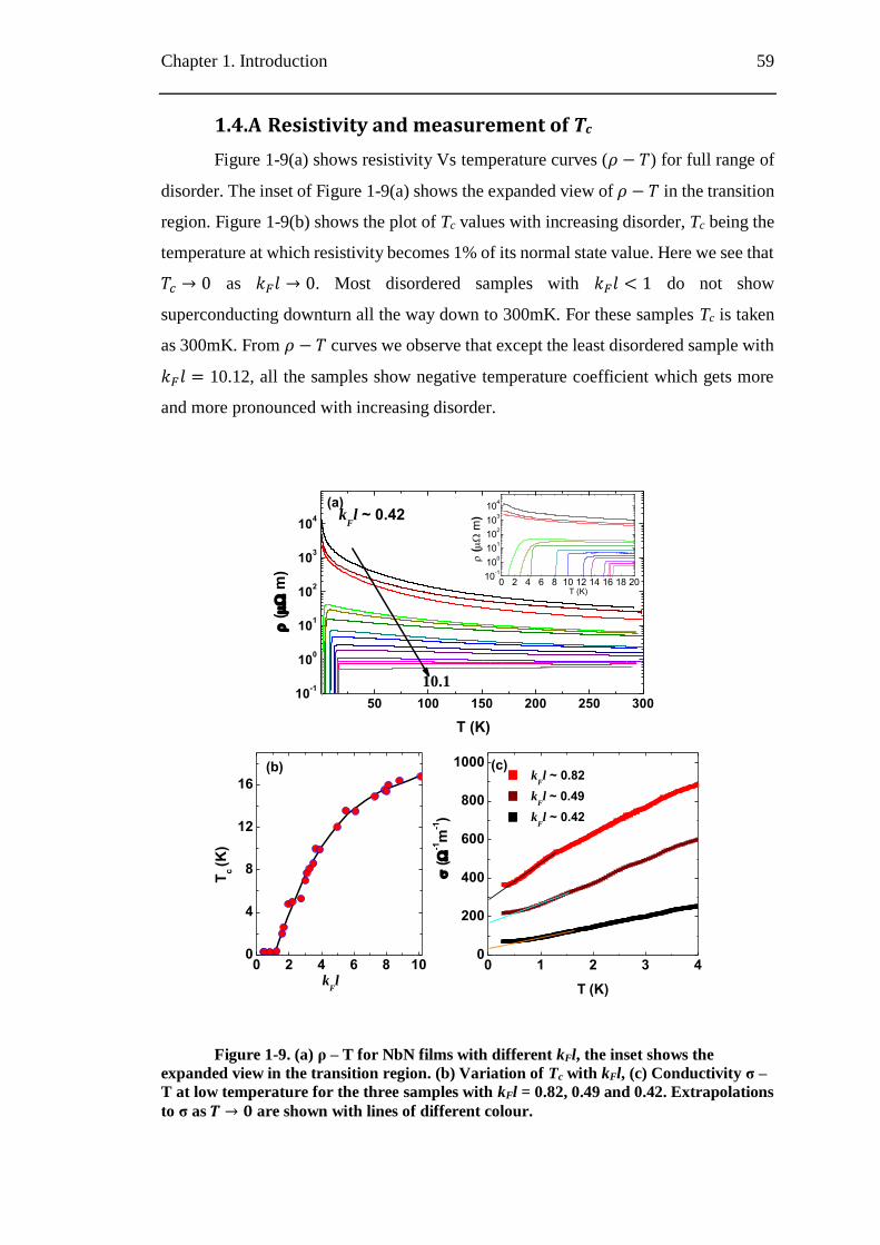
Chapter 1. Introduction 59
1.4.A Resistivity and measurement of Tc
Figure 1-9(a) shows resistivity Vs temperature curves (𝜌 − 𝑇) for full range of
disorder. The inset of Figure 1-9(a) shows the expanded view of 𝜌 − 𝑇 in the transition
region. Figure 1-9(b) shows the plot of Tc values with increasing disorder, Tc being the
temperature at which resistivity becomes 1% of its normal state value. Here we see that
𝑇𝑐 → 0 as 𝑘𝐹𝑙 → 0. Most disordered samples with 𝑘𝐹𝑙 < 1 do not show
superconducting downturn all the way down to 300mK. For these samples Tc is taken
as 300mK. From 𝜌 − 𝑇 curves we observe that except the least disordered sample with
𝑘𝐹𝑙 = 10.12, all the samples show negative temperature coefficient which gets more
and more pronounced with increasing disorder.
50 100 150 200 250 30010
-1
100
101
102
103
104
0 2 4 6 8 100
4
8
12
16
0 1 2 3 40
200
400
600
800
1000
0 2 4 6 8 10 12 14 16 18 2010
-1
100
101
102
103
104
10.1
(
m)
T (K)
kFl ~ 0.42
(a)
(b)
Tc (K
)
kFl
(c)
kFl ~ 0.82
kFl ~ 0.49
kFl ~ 0.42
(
-1m
-1)
T (K)
(
m)
T (K)
Figure 1-9. (a) ρ – T for NbN films with different kFl, the inset shows the
expanded view in the transition region. (b) Variation of Tc with kFl, (c) Conductivity σ –
T at low temperature for the three samples with kFl = 0.82, 0.49 and 0.42. Extrapolations
to σ as 𝑻 → 𝟎 are shown with lines of different colour.
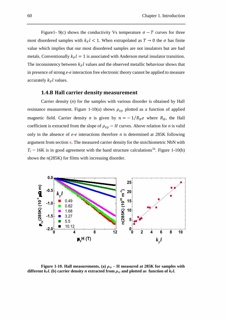
60 Chapter 1. Introduction
Figure1- 9(c) shows the conductivity Vs temperature 𝜎 − 𝑇 curves for three
most disordered samples with 𝑘𝐹𝑙 < 1. When extrapolated as 𝑇 → 0 the 𝜎 has finite
value which implies that our most disordered samples are not insulators but are bad
metals. Conventionally 𝑘𝐹𝑙 = 1 is associated with Anderson metal insulator transition.
The inconsistency between 𝑘𝐹𝑙 values and the observed metallic behaviour shows that
in presence of strong e-e interaction free electronic theory cannot be applied to measure
accurately 𝑘𝐹𝑙 values.
1.4.B Hall carrier density measurement
Carrier density (n) for the samples with various disorder is obtained by Hall
resistance measurement. Figure 1-10(a) shows 𝜌𝑥𝑦 plotted as a function of applied
magnetic field. Carrier density n is given by 𝑛 = −1 𝑅𝐻𝑒⁄ where 𝑅𝐻, the Hall
coefficient is extracted from the slope of 𝜌𝑥𝑦 −𝐻 curves. Above relation for n is valid
only in the absence of e-e interactions therefore n is determined at 285K following
argument from section x. The measured carrier density for the stoichiometric NbN with
Tc ~ 16K is in good agreement with the band structure calculations56. Figure 1-10(b)
shows the n(285K) for films with increasing disorder.
0 4 8 12-2.0
-1.5
-1.0
-0.5
0.0
0 2 4 6 8 100
5
10
15
20
25
0.49
0.82
1.68
3.27
5.5
10.12xy(2
85K
) (1
0-3
m)
0H (T)
kFl
n(2
85
K)
(10
28 m
-3)
kFl
Figure 1-10. Hall measurements, (a) ρxy – H measured at 285K for samples with
different kFl. (b) carrier density n extracted from ρxy and plotted as function of kFl.
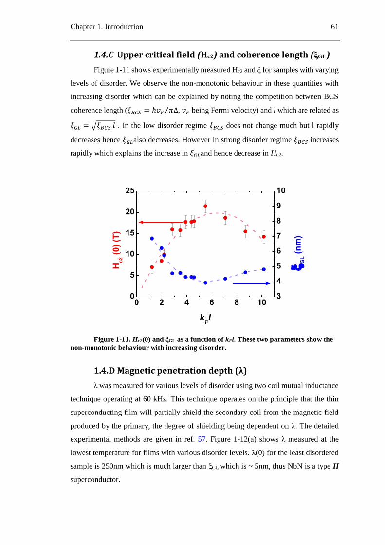
Chapter 1. Introduction 61
1.4.C Upper critical field (Hc2) and coherence length (ξGL)
Figure 1-11 shows experimentally measured Hc2 and ξ for samples with varying
levels of disorder. We observe the non-monotonic behaviour in these quantities with
increasing disorder which can be explained by noting the competition between BCS
coherence length (𝜉𝐵𝐶𝑆 = ℏ𝑣𝐹 𝜋∆⁄ , 𝑣𝐹 being Fermi velocity) and l which are related as
𝜉𝐺𝐿 = √𝜉𝐵𝐶𝑆 𝑙 . In the low disorder regime 𝜉𝐵𝐶𝑆 does not change much but l rapidly
decreases hence 𝜉𝐺𝐿also decreases. However in strong disorder regime 𝜉𝐵𝐶𝑆 increases
rapidly which explains the increase in 𝜉𝐺𝐿and hence decrease in Hc2.
0 2 4 6 8 100
5
10
15
20
25
Hc
2 (
0)
(T)
kFl
3
4
5
6
7
8
9
10
G
L (
nm
)
Figure 1-11. Hc2(0) and ξGL as a function of kFl. These two parameters show the
non-monotonic behaviour with increasing disorder.
1.4.D Magnetic penetration depth (λ)
λ was measured for various levels of disorder using two coil mutual inductance
technique operating at 60 kHz. This technique operates on the principle that the thin
superconducting film will partially shield the secondary coil from the magnetic field
produced by the primary, the degree of shielding being dependent on λ. The detailed
experimental methods are given in ref. 57. Figure 1-12(a) shows λ measured at the
lowest temperature for films with various disorder levels. λ(0) for the least disordered
sample is 250nm which is much larger than ξGL which is ~ 5nm, thus NbN is a type II
superconductor.
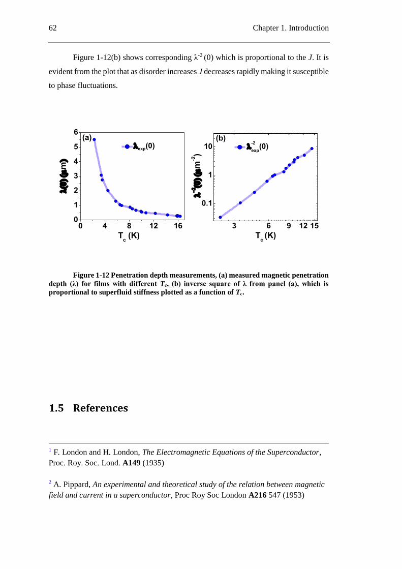
62 Chapter 1. Introduction
Figure 1-12(b) shows corresponding λ-2 (0) which is proportional to the J. It is
evident from the plot that as disorder increases J decreases rapidly making it susceptible
to phase fluctuations.
3 6 9 12 15
0.1
1
10 -2
exp(0)
m-2)
Tc (K)
0 4 8 12 160
1
2
3
4
5
6(b)
exp(0)
m
Tc (K)
(a)
Figure 1-12 Penetration depth measurements, (a) measured magnetic penetration
depth (λ) for films with different Tc, (b) inverse square of λ from panel (a), which is
proportional to superfluid stiffness plotted as a function of Tc.
1.5 References
1 F. London and H. London, The Electromagnetic Equations of the Superconductor,
Proc. Roy. Soc. Lond. A149 (1935)
2 A. Pippard, An experimental and theoretical study of the relation between magnetic
field and current in a superconductor, Proc Roy Soc London A216 547 (1953)
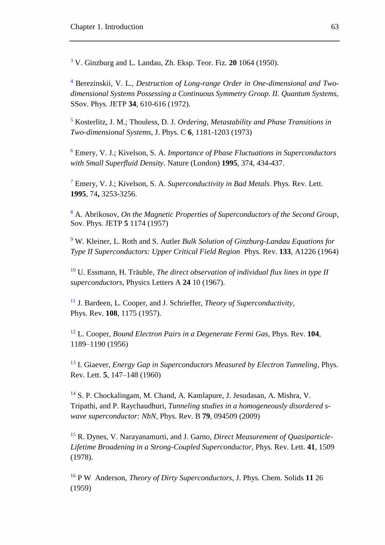
Chapter 1. Introduction 63
3 V. Ginzburg and L. Landau, Zh. Eksp. Teor. Fiz. 20 1064 (1950).
4 Berezinskii, V. L., Destruction of Long-range Order in One-dimensional and Two-
dimensional Systems Possessing a Continuous Symmetry Group. II. Quantum Systems,
SSov. Phys. JETP 34, 610-616 (1972).
5 Kosterlitz, J. M.; Thouless, D. J. Ordering, Metastability and Phase Transitions in
Two-dimensional Systems, J. Phys. C 6, 1181-1203 (1973)
6 Emery, V. J.; Kivelson, S. A. Importance of Phase Fluctuations in Superconductors
with Small Superfluid Density. Nature (London) 1995, 374, 434-437.
7 Emery, V. J.; Kivelson, S. A. Superconductivity in Bad Metals. Phys. Rev. Lett.
1995, 74, 3253-3256.
8 A. Abrikosov, On the Magnetic Properties of Superconductors of the Second Group,
Sov. Phys. JETP 5 1174 (1957)
9 W. Kleiner, L. Roth and S. Autler Bulk Solution of Ginzburg-Landau Equations for
Type II Superconductors: Upper Critical Field Region Phys. Rev. 133, A1226 (1964)
10 U. Essmann, H. Träuble, The direct observation of individual flux lines in type II
superconductors, Physics Letters A 24 10 (1967).
11 J. Bardeen, L. Cooper, and J. Schrieffer, Theory of Superconductivity,
Phys. Rev. 108, 1175 (1957).
12 L. Cooper, Bound Electron Pairs in a Degenerate Fermi Gas, Phys. Rev. 104,
1189–1190 (1956)
13 I. Giaever, Energy Gap in Superconductors Measured by Electron Tunneling, Phys.
Rev. Lett. 5, 147–148 (1960)
14 S. P. Chockalingam, M. Chand, A. Kamlapure, J. Jesudasan, A. Mishra, V.
Tripathi, and P. Raychaudhuri, Tunneling studies in a homogeneously disordered s-
wave superconductor: NbN, Phys. Rev. B 79, 094509 (2009)
15 R. Dynes, V. Narayanamurti, and J. Garno, Direct Measurement of Quasiparticle-
Lifetime Broadening in a Strong-Coupled Superconductor, Phys. Rev. Lett. 41, 1509
(1978).
16 P W Anderson, Theory of Dirty Superconductors, J. Phys. Chem. Solids 11 26
(1959)
64 Chapter 1. Introduction
17 B. Bishop, E. Spencer and R. Dynes, The metal-insulator transition in amorphous
Nb:Si, Solid State Electron. 28 73 (1985); G. Hertel, D. Bishop, E. Spencer, J.
Rowell and R. Dynes, Tunneling and Transport Measurements at the Metal-
Insulator Transition of Amorphous Nb: Si, Phys. Rev. Lett. 50 743 (1983)
18 T. Furubayashi, N. Nishida, M. Yamaguchi, K. Morigaki and H. Ishimoto,
Superconducting properties of amorphous Si1−xAux near metal-insulator transition,
Solid State Commun. 55 513 (1985)
19 J. Lesueur, L. Dumoulin and P. Nedellec, Superconductivity near the Metal-
Insulator Transition in quench condensed AlxGe1-x, Solid State Commun. 66 723
(1988)
20 S. P. Chockalingam, M. Chand, J. Jesudasan, V. Tripathi and P. Raychaudhuri,
Superconducting properties and Hall effect of epitaxial NbN thin films, Phys. Rev. B
77 214503 (2008)
21 A. M. Goldman and N Markovic, Superconductor Insulator Transitions in the Two
Dimensional Limit, Phys. Today 51(11) 39 (1998).
22 Haviland, D. B.; Liu Y.; Goldman, A. M. Onset of Superconductivity in the Two-
Dimensional Limit. Phys. Rev. Lett. 62, 2180 (1989)
23 Paalanen, M. A.; Hebard, A. F.; Ruel, R. R. Low Temperature Insulating Phases of
Uniformly Disordered Two-Dimensional Superconductors. Phys. Rev. Lett. 1992, 69,
1604-1607.
24 Hebard, A. F.; Paalanen, M. A. Magnetic-Field-Tuned Superconductor-Insulator
Transition in Two-Dimensional Films. Phys. Rev. Lett. 1990, 65, 927-930.
25 M. Chand, G. Saraswat, A. Kamlapure, M. Mondal, S. Kumar, J. Jesudasan, V.
Bagwe, L. Benfatto, V. Tripathi, and P. Raychaudhuri, Phase diagram of a strongly
disordered s-wave superconductor, NbN, close to the metal-insulator transition. Phys.
Rev. B 85, 014508 (2012).
26 Crauste, O.; Marrache-Kikuchi, C. A.; Berg´e, L.; Collin, S.; Dolgorouky, Y.;
Marnieros, S.; Nones, C.; Dumoulin, L. Tunable superconducting properties of a-
NbSi thin films and application to detection in astrophysics, J. Low Temp. Physics
2011, 163, 60-66.
27 R. Crane, N. P. Armitage, A. Johansson, G. Sambandamurthy, D. Shahar, and G.
Grüner, Survival of superconducting correlations across the two-dimensional
Chapter 1. Introduction 65
superconductor-insulator transition: A finite-frequency study, Phys. Rev. B 75,
184530 (2007)
28 W. Liu, M. Kim, G. Sambandamurthy, and N. P. Armitage, Dynamical study of
phase fluctuations and their critical slowing down in amorphous superconducting
films, Phys. Rev. B 84 024511 (2011)
29 B. Sacépé, C. Chapelier, T. I. Baturina, V. M. Vinokur, M. R. Baklanov, and M.
Sanquer, Pseudogap in a thin film of a conventional superconductor, Nat. Comm. 1
140 (2010)
30 B. Sacépé, T. Dubouchet, C. Chapelier, M. Sanquer, M. Ovadia, D. Shahar, M.
Feigel'man, and L. Ioffe, Localization of preformed Cooper pairs in disordered
superconductors, Nature Physics 7, 239–244 (2011)
31 M. Mondal, A. Kamlapure, M. Chand, G. Saraswat, S. Kumar, J. Jesudasan, L.
Benfatto, V. Tripathi and P. Raychaudhuri, Phase fluctuations in a strongly
disordered s-wave NbN superconductor close to the Metal-Insulator transition, Phys.
Rev. Lett. 106, 047001 (2011).
32 D. Shahar and Z. Ovadyahu, Superconductivity near the mobility edge, Phys. Rev.
B 46, 10917–10922 (1992)
33 G. Sambandamurthy, L. W. Engel, A. Johansson, E. Peled, and D. Shahar
Experimental Evidence for a Collective Insulating State in Two-Dimensional
Superconductors, Phys. Rev. Lett. 94 017003 (2005)
34 T. I. Baturina, C. Strunk, M. R. Baklanov and A. Satta, Quantum Metallicity on the
High-Field Side of the Superconductor-Insulator Transition, Phys. Rev. Lett. 98,
127003 (2007)
35 H. Q. Nguyen, S. M. Hollen, M. D. Stewart, Jr., J. Shainline, Aijun Yin, J. M. Xu,
and J. M. Valles, Jr., Observation of Giant Positive Magnetoresistance in a Cooper
Pair Insulator, Phys. Rev. Lett. 103, 157001 (2009)
36 M. D. Stewart Jr., A. Yin, J. M. Xu, and J. M. Valles Jr., Superconducting Pair
Correlations in an Amorphous Insulating Nanohoneycomb Film, Science 318 1273
(2007)
37 S. M. Hollen, H. Q. Nguyen, E. Rudisaile, M. D. Stewart, Jr., J. Shainline, J. M. Xu
and J. M. Valles, Jr., Cooper-pair insulator phase in superconducting amorphous Bi
films induced by nanometer-scale thickness variations, Phys. Rev. B 84, 064528
(2011)
66 Chapter 1. Introduction
38 S. Poran, E. Shimshoni, and A. Frydman, Disorder-induced superconducting
ratchet effect in nanowires, Phys. Rev. B 84, 014529 (2011).
39 D. Sherman, G. Kopnov, D. Shahar, and A. Frydman, Measurement of a
Superconducting Energy Gap in a Homogeneously Amorphous Insulator, Phys. Rev.
Lett. 108, 177006
40 P. W. Anderson, K. A. Muttalib, and T. V. Ramakrishnan, Theory of the
"universal" degradation of Tc in high-temperature superconductors, Phys. Rev. B 28
117 (1983)
41 A. M. Finkelstein, Suppression of superconductivity in homogeneously disordered
systems, Phys. B 197 636 (1994)
42 M, Ma and P. Lee, Localized superconductors, Phys. Rev. B 32 5658 (1985)
43 A. Ghosal, M. Randeria, and N. Trivedi, Inhomogeneous pairing in highly
disordered s-wave superconductors, Phys. Rev. B 65, 014501 (2001).
44 Y. Dubi, Y. Meir, and Y. Avishai, Island formation in disordered superconducting
thin films at finite magnetic fields, Phys. Rev. B 78, 024502 (2008).
45 K. Bouadim, Y. L. Loh, M. Randeria, and N. Trivedi, Single- and two-particle
energy gaps across the disorder-driven superconductor–insulator transition, Nat.
Phys. 7, 884 (2011).
46 G. Seibold, L. Benfatto, C. Castellani, and J. Lorenzana, Superfluid Density and
Phase Relaxation in Superconductors with Strong Disorder, Phys. Rev. Lett. 108,
207004 (2012).
47 M. P. A. Fisher, G. Grinstein, and S. M. Girvin, Presence of quantum diffusion in
two dimensions: Universal resistance at the superconductor-insulator transition,
Phys. Rev. Lett. 64, 587 (1990).
48 L. B. Ioffe and M. M´ezard, Disorder-Driven Quantum Phase Transitions in
Superconductors and Magnets, Phys. Rev. Lett. 105, 037001 (2010).
49 M. V. Feigel’man, L. B. Ioffe, and M. M´ezard, Superconductor-insulator
transition and energy localization, Phys. Rev. B 82, 184534 (2010).
50 A. Ghosal, M. Randeria, and N. Trivedi, Role of Spatial Amplitude Fluctuations in
Highly Disordered s-Wave Superconductors, Phys. Rev. Lett. 81, 3940 (1998)
Chapter 1. Introduction 67
51 S. P. Chockalingam, M. Chand, J. Jesudasan, V. Tripathi, and P. Raychaudhuri,
Superconducting properties and Hall effect of epitaxial NbN thin films, Phys. Rev. B
77, 214503 (2008)
52 M. Chand, A. Mishra, Y. M. Xiong, A. Kamlapure, S. P. Chockalingam, J.
Jesudasan, V. Bagwe, M. Mondal, P. W. Adams, V. Tripathi, and P. Raychaudhuri,
Temperature dependence of resistivity and Hall coefficient in strongly disordered
NbN thin films, Phys. Rev. B 80, 134514 (2009).
53 M. Mondal, M. Chand, A. Kamlapure, J. Jesudasan, V. C. Bagwe, S. Kumar, G.
Saraswat, V. Tripathi and P. Raychaudhuri, Phase Diagram and Upper Critical Field
of Homogeneously Disordered Epitaxial 3-Dimensional NbN Films, J. Supercond.
Nov. Magn. 24, 341 (2011).
54 Madhavi Chand, Ph.D. Thesis, Tata Institute of Fundamental Research, 2013
http://www.tifr.res.in/~superconductivity/pdfs/madhavi.pdf
55 M. A. Khodas and A. M. Finkelstein, Hall coefficient in an interacting electron
gas, Phys. Rev. B 68 155114 (2003).
56 L. F. Mattheiss, Electronic Band Structure of Niobium Nitride, Phys. Rev. B 5, 315
(1972).
57 A. Kamlapure, M. Mondal, M. Chand, A. Mishra, J. Jesudasan, V. Bagwe, L.
Benfatto, V. Tripathi, and P. Raychaudhuri, Measurement of magnetic penetration
depth and superconducting energy gap in very thin epitaxial NbN films, Appl. Phys.
Lett. 96, 072509 (2010).
Chapter 2
Scanning tunneling microscope
The Scanning Tunneling Microscope (STM) invented in 1983 by Binnig and
Rohrer1,2,3 at IBM Zurich has been proven to be the most important tool for surface
investigations. The first experiment showing atomically resolved Si(111) which
confirmed 7×7 surface reconstruction4 and later experiments demonstrated the
unsurpassed spatial power of STM. Using the combination of scanning tunneling
microscopy and scanning tunneling spectroscopy (STS), number of interesting
experiments have been carried demonstrating the capability of the instrument. These
include building structures at the atomic level using the technique of atom
manipulation5, visualising standing wave pattern formed by electron surface states in
an artificial quantum corral6,7 , first direct evidence of Kondo resonance at the magnetic
impurity on metal surface8, spectroscopic mapping of vortex core in Abrikosov lattice
in Type-II superconductors9 etc.
Spatially resolved spectroscopy measurements performed at the atomic scale
has provided the excellent insight into the physics of strongly correlated electron
systems, especially high temperature cuprate superconductors. Other related techniques
include spin polarized scanning tunneling microscope10 (SP-STM) which is powerful
tool to determine spin texture of the surface at the atomic level. Recently combination
of STM and non-contact atomic force microscopy (nc-AFM) has provided the
unprecedented spatial resolution11,12 along with spectroscopic information which
enabled imaging of single molecules and real space evolution of organic reactions. In
this chapter I will summarize the operating principles of STM and STS and then
describe the development and characterization of low temperature, high vacuum
scanning tunneling microscope (LT-STM).
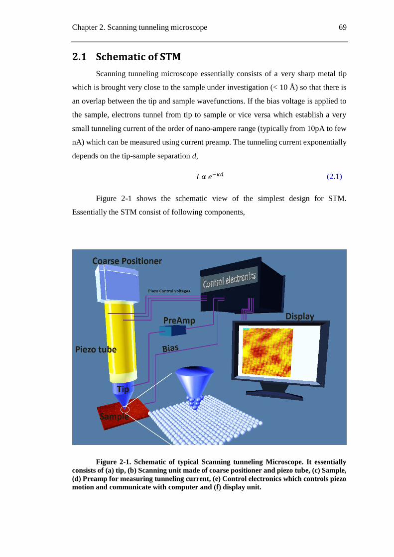
Chapter 2. Scanning tunneling microscope 69
2.1 Schematic of STM
Scanning tunneling microscope essentially consists of a very sharp metal tip
which is brought very close to the sample under investigation (< 10 Å) so that there is
an overlap between the tip and sample wavefunctions. If the bias voltage is applied to
the sample, electrons tunnel from tip to sample or vice versa which establish a very
small tunneling current of the order of nano-ampere range (typically from 10pA to few
nA) which can be measured using current preamp. The tunneling current exponentially
depends on the tip-sample separation d,
𝐼 𝛼 𝑒−𝜅𝑑 (2.1)
Figure 2-1 shows the schematic view of the simplest design for STM.
Essentially the STM consist of following components,
Figure 2-1. Schematic of typical Scanning tunneling Microscope. It essentially
consists of (a) tip, (b) Scanning unit made of coarse positioner and piezo tube, (c) Sample,
(d) Preamp for measuring tunneling current, (e) Control electronics which controls piezo
motion and communicate with computer and (f) display unit.
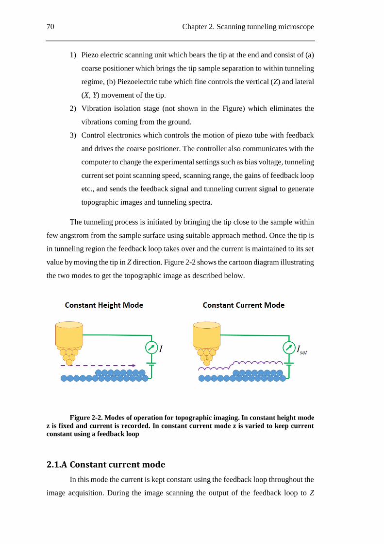
70 Chapter 2. Scanning tunneling microscope
1) Piezo electric scanning unit which bears the tip at the end and consist of (a)
coarse positioner which brings the tip sample separation to within tunneling
regime, (b) Piezoelectric tube which fine controls the vertical (Z) and lateral
(X, Y) movement of the tip.
2) Vibration isolation stage (not shown in the Figure) which eliminates the
vibrations coming from the ground.
3) Control electronics which controls the motion of piezo tube with feedback
and drives the coarse positioner. The controller also communicates with the
computer to change the experimental settings such as bias voltage, tunneling
current set point scanning speed, scanning range, the gains of feedback loop
etc., and sends the feedback signal and tunneling current signal to generate
topographic images and tunneling spectra.
The tunneling process is initiated by bringing the tip close to the sample within
few angstrom from the sample surface using suitable approach method. Once the tip is
in tunneling region the feedback loop takes over and the current is maintained to its set
value by moving the tip in Z direction. Figure 2-2 shows the cartoon diagram illustrating
the two modes to get the topographic image as described below.
Figure 2-2. Modes of operation for topographic imaging. In constant height mode
z is fixed and current is recorded. In constant current mode z is varied to keep current
constant using a feedback loop
2.1.A Constant current mode
In this mode the current is kept constant using the feedback loop throughout the
image acquisition. During the image scanning the output of the feedback loop to Z
Chapter 2. Scanning tunneling microscope 71
electrode of the piezo tube are transformed to get the vertical position as a function of
lateral position Z(X, Y). Corrugation amplitude is defined as difference between
smallest and largest tip sample-distance in constant current image. Since the tunneling
current exponentially depends on the separation between tip and sample, the
corrugation amplitudes < 0.1 Å can be obtained using STM.
2.1.B Constant height mode
In this mode the vertical position of the tip is kept fixed throughout the scan and
the current is measured as at each location to get the topographic image. This mode is
suitable only for small area with flat surface as there is risk of tip crashing. This mode
has an advantage that the images can be acquired with extremely high scan speeds
thereby reducing the time for acquiring the image.
2.2 STM Theory
As a first approximation STM can be modelled as a finite barrier potential
problem in 1D with an electron with mass m and energy E incident from left on the
rectangular potential barrier of width d and height V0 (Figure 2-3). The solution of
Schrödinger wave equation for the three regions is given by,
𝜑𝐼 = 𝐴𝐼𝑒𝑖𝑘𝑥 (2.2)
𝜑𝐼𝐼 = 𝐴𝐼𝐼𝑒𝜅𝑥 + 𝐴𝐼𝐼
′𝑒−𝜅𝑥 (2.3)
𝜑𝐼𝐼𝐼 = 𝐴𝐼𝐼𝐼𝑒𝑘𝑥 + 𝐴𝐼𝐼𝐼
′𝑒−𝑖𝑘𝑥 (2.4)
where,
𝑘 = √2𝑚𝐸
ℏ2 and 𝜅 = √
2𝑚(𝑉0 − 𝐸)
ℏ2 (2.5)
The coefficients A’s are found using appropriate boundary conditions. The
transmission coefficient T which is proportional can be given as13,
𝑇 = |𝐴𝐼𝐼𝐼𝐴𝐼|2
=4𝐸(𝑉0 − 𝐸)
4𝐸(𝑉0 − 𝐸) + 𝑉02 sinh2 𝜅𝑑
(2.6)
We see that for STM d ~ 5 Å, V0 =4 eV, only the sinh term dominates and one
gets,
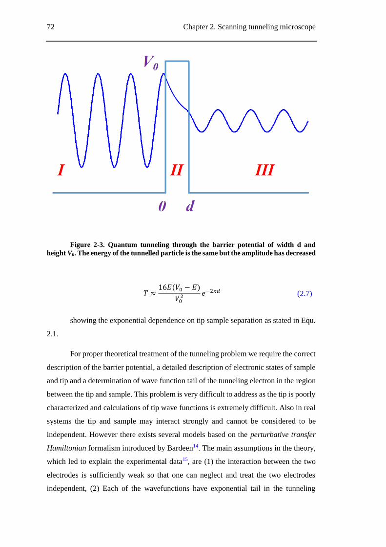
72 Chapter 2. Scanning tunneling microscope
Figure 2-3. Quantum tunneling through the barrier potential of width d and
height V0. The energy of the tunnelled particle is the same but the amplitude has decreased
𝑇 ≈16𝐸(𝑉0 − 𝐸)
𝑉02 𝑒−2𝜅𝑑 (2.7)
showing the exponential dependence on tip sample separation as stated in Equ.
2.1.
For proper theoretical treatment of the tunneling problem we require the correct
description of the barrier potential, a detailed description of electronic states of sample
and tip and a determination of wave function tail of the tunneling electron in the region
between the tip and sample. This problem is very difficult to address as the tip is poorly
characterized and calculations of tip wave functions is extremely difficult. Also in real
systems the tip and sample may interact strongly and cannot be considered to be
independent. However there exists several models based on the perturbative transfer
Hamiltonian formalism introduced by Bardeen14. The main assumptions in the theory,
which led to explain the experimental data15, are (1) the interaction between the two
electrodes is sufficiently weak so that one can neglect and treat the two electrodes
independent, (2) Each of the wavefunctions have exponential tail in the tunneling
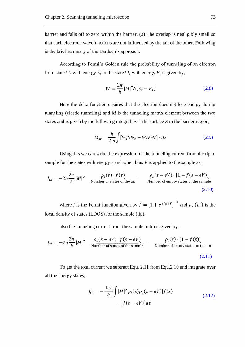
Chapter 2. Scanning tunneling microscope 73
barrier and falls off to zero within the barrier, (3) The overlap is negligibly small so
that each electrode wavefunctions are not influenced by the tail of the other. Following
is the brief summary of the Bardeen’s approach.
According to Fermi’s Golden rule the probability of tunneling of an electron
from state Ψ𝑡 with energy Et to the state Ψ𝑠 with energy Es is given by,
𝑊 =2𝜋
ℏ|𝑀|2𝛿(E𝑡 − 𝐸𝑠) (2.8)
Here the delta function ensures that the electron does not lose energy during
tunneling (elastic tunneling) and M is the tunneling matrix element between the two
states and is given by the following integral over the surface S in the barrier region,
𝑀𝑠𝑡 =ℏ
2𝑚∫[Ψ𝑠
∗∇Ψ𝑡 −Ψ𝑡∇Ψ𝑠∗] ∙ 𝑑𝑆 (2.9)
Using this we can write the expression for the tunneling current from the tip to
sample for the states with energy ε and when bias V is applied to the sample as,
𝐼𝑡𝑠 = −2𝑒2𝜋
ℏ|𝑀|2
𝜌𝑡(휀) ∙ 𝑓(휀)⏟ Number of states of the tip
∙
𝜌𝑠(휀 − 𝑒𝑉) ∙ [1 − 𝑓(휀 − 𝑒𝑉)]⏟ Number of empty states of the sample
(2.10)
where f is the Fermi function given by 𝑓 = [1 + 𝑒𝜀 𝑘𝐵𝑇⁄ ]−1
and 𝜌𝑆 (𝜌𝑡) is the
local density of states (LDOS) for the sample (tip).
also the tunneling current from the sample to tip is given by,
𝐼𝑠𝑡 = −2𝑒2𝜋
ℏ|𝑀|2
𝜌𝑠(휀 − 𝑒𝑉) ∙ 𝑓(휀 − 𝑒𝑉)⏟ Number of states of the sample
∙
𝜌𝑡(휀) ∙ [1 − 𝑓(휀)]⏟ Number of empty states of the tip
(2.11)
To get the total current we subtract Equ. 2.11 from Equ.2.10 and integrate over
all the energy states,
𝐼𝑡𝑠 = −
4𝜋𝑒
ℏ∫|𝑀|2 𝜌𝑡(휀)𝜌𝑠(휀 − 𝑒𝑉)[𝑓(휀)
− 𝑓(휀 − 𝑒𝑉)]𝑑휀
(2.12)
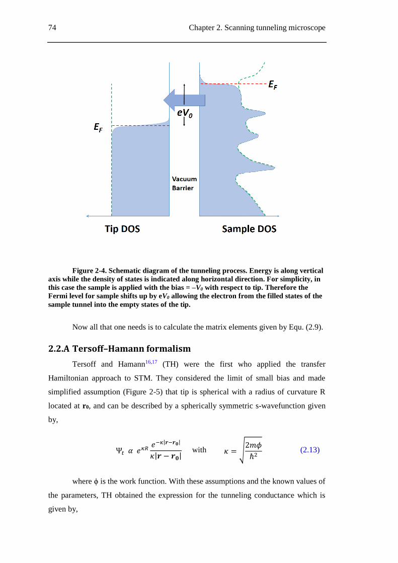
74 Chapter 2. Scanning tunneling microscope
Figure 2-4. Schematic diagram of the tunneling process. Energy is along vertical
axis while the density of states is indicated along horizontal direction. For simplicity, in
this case the sample is applied with the bias = ‒V0 with respect to tip. Therefore the
Fermi level for sample shifts up by eV0 allowing the electron from the filled states of the
sample tunnel into the empty states of the tip.
Now all that one needs is to calculate the matrix elements given by Equ. (2.9).
2.2.A Tersoff–Hamann formalism
Tersoff and Hamann16,17 (TH) were the first who applied the transfer
Hamiltonian approach to STM. They considered the limit of small bias and made
simplified assumption (Figure 2-5) that tip is spherical with a radius of curvature R
located at r0, and can be described by a spherically symmetric s-wavefunction given
by,
Ψ𝑡 𝛼 𝑒𝜅𝑅𝑒−𝜅|𝒓−𝒓𝟎|
𝜅|𝒓 − 𝒓𝟎| with 𝜅 = √
2𝑚𝜙
ℏ2 (2.13)
where ϕ is the work function. With these assumptions and the known values of
the parameters, TH obtained the expression for the tunneling conductance which is
given by,
Chapter 2. Scanning tunneling microscope 75
Figure 2-5. Schematic view of the tunneling geometry within Tersoff – Hamann
model. Tip may have arbitrary shape but it is spherical at the end. Radius of curvature
of the tip is R and the center of the curvature is at r0. Nearest distance between the tip
and sample is d.
𝐺𝑡 ≡𝐼𝑡𝑉𝑡≈ 0.1𝑅2 ∙ 𝑒2𝜅𝑅𝜌𝑆(𝒓𝟎 , 𝐸𝐹) (2.14)
with 𝜌𝑆(𝒓𝟎 , 𝐸) = ∑|Ψ𝑠|2 𝛿(𝐸𝑠 − 𝐸)
𝑠
(2.15)
where 𝜌𝑆(𝒓𝟎 , 𝐸𝐹) is the LDOS of the sample at Fermi level evaluated at the
centre of the tip 𝒓𝟎. Therefore within TH model, constant current mode image has
simple interpretation as contours of constant 𝜌𝑆(𝒓𝟎 , 𝐸𝐹) of the surface and it reflect
only the sample properties.
2.2.B Other models
With known experimental parameters: R = 9 Å, tip center to top layer distance
= 15 Å and with low bias it was shown that16,17 s-wave tip model is not sufficient to
resolve features smaller than 6 Å and it fails to explain previously observed atomically
resolved images. However it has been shown that the atomically resolved imaging of
76 Chapter 2. Scanning tunneling microscope
closed packed structures can be obtained by using the tip which has more directed
wavefunction (e.g. 𝑑𝑧2 state)18. In 1988 Chen19,20,21 proposed simpler way to
approximate the tunneling matrix elements where he showed that by expanding vacuum
tail of the tip wave functions in terms of spherical harmonics, tunneling matrix elements
can be expressed as a derivative of the sample wave functions at the centre of the apex
atom. Following table shows the tunneling matrix elements evaluated for different tip
wave functions,
State M α value at r0
s 𝜓
p [z] 𝜕𝜓
𝜕𝑧
d [𝑧2 −1
3𝑟2]
𝜕2𝜓
𝜕𝑧2−1
3𝜅2𝜓
Table 2.1 Tunneling matrix elements for different tip states
2.3 Fabrication of low temperature STM
Over the past few years there are reports of construction of
STM22,23,24,25,26,27,28,29,30,31 which can reach temperatures below 1K incorporating in-situ
cleaving and surface cleaning of single crystals and thin film deposition capabilities.
However, a design that allows measurements to be performed on in-situ grown
superconducting films on insulating substrates has remained a challenge. The study of
superconducting thin films on insulating substrates is important for several reasons.
The two important reasons are,
Single crystalline substrates of insulating MgO, SrTiO3 and LaAlO3 remain
the most popular choice for growing lattice matched high-quality epitaxial
thin films of several superconductors used for basic studies and
applications, such as YBa2Cu3O7, (La,Sr)2CuO4 and NbN.
The superconducting transition temperature of a superconductor in contact
with a normal metal is suppressed through proximity effect up to a depth of
the order of the coherence length, from the interface. Since few
nanometers to a few hundred nanometers), is in the same range of the
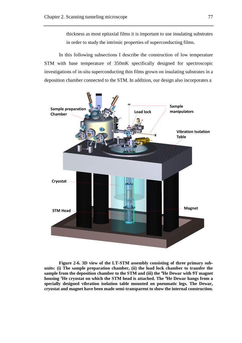
Chapter 2. Scanning tunneling microscope 77
thickness as most epitaxial films it is important to use insulating substrates
in order to study the intrinsic properties of superconducting films.
In this following subsections I describe the construction of low temperature
STM with base temperature of 350mK specifically designed for spectroscopic
investigations of in-situ superconducting thin films grown on insulating substrates in a
deposition chamber connected to the STM. In addition, our design also incorporates a
Sample preparation Chamber
Sample manipulators
Vibration Isolation Table
Cryostat
Load lock
STM HeadMagnet
Figure 2-6. 3D view of the LT-STM assembly consisting of three primary sub-
units: (i) The sample preparation chamber, (ii) the load lock chamber to transfer the
sample from the deposition chamber to the STM and (iii) the 4He Dewar with 9T magnet
housing 3He cryostat on which the STM head is attached. The 4He Dewar hangs from a
specially designed vibration isolation table mounted on pneumatic legs. The Dewar,
cryostat and magnet have been made semi-transparent to show the internal construction.
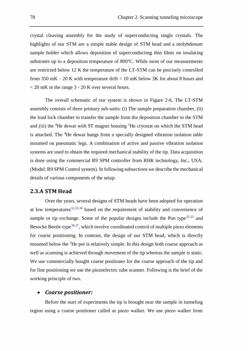
78 Chapter 2. Scanning tunneling microscope
crystal cleaving assembly for the study of superconducting single crystals. The
highlights of our STM are a simple stable design of STM head and a molybdenum
sample holder which allows deposition of superconducting thin films on insulating
substrates up to a deposition temperature of 800ºC. While most of our measurements
are restricted below 12 K the temperature of the LT-STM can be precisely controlled
from 350 mK – 20 K with temperature drift < 10 mK below 3K for about 8 hours and
< 20 mK in the range 3 - 20 K over several hours.
The overall schematic of our system is shown in Figure 2-6. The LT-STM
assembly consists of three primary sub-units: (i) The sample preparation chamber, (ii)
the load lock chamber to transfer the sample from the deposition chamber to the STM
and (iii) the 4He dewar with 9T magnet housing 3He cryostat on which the STM head
is attached. The 4He dewar hangs from a specially designed vibration isolation table
mounted on pneumatic legs. A combination of active and passive vibration isolation
systems are used to obtain the required mechanical stability of the tip. Data acquisition
is done using the commercial R9 SPM controller from RHK technology, Inc., USA.
(Model: R9 SPM Control system). In following subsections we describe the mechanical
details of various components of the setup.
2.3.A STM Head
Over the years, several designs of STM heads have been adopted for operation
at low temperatures32,33,34 based on the requirement of stability and convenience of
sample or tip exchange. Some of the popular designs include the Pan type22,35 and
Besocke Beetle-type36,37, which involve coordinated control of multiple piezo elements
for coarse positioning. In contrast, the design of our STM head, which is directly
mounted below the 3He pot is relatively simple. In this design both coarse approach as
well as scanning is achieved through movement of the tip whereas the sample is static.
We use commercially bought coarse positioner for the coarse approach of the tip and
for fine positioning we use the piezoelectric tube scanner. Following is the brief of the
working principle of two.
Coarse positioner:
Before the start of experiments the tip is brought near the sample in tunneling
region using a coarse positioner called as piezo walker. We use piezo walker from
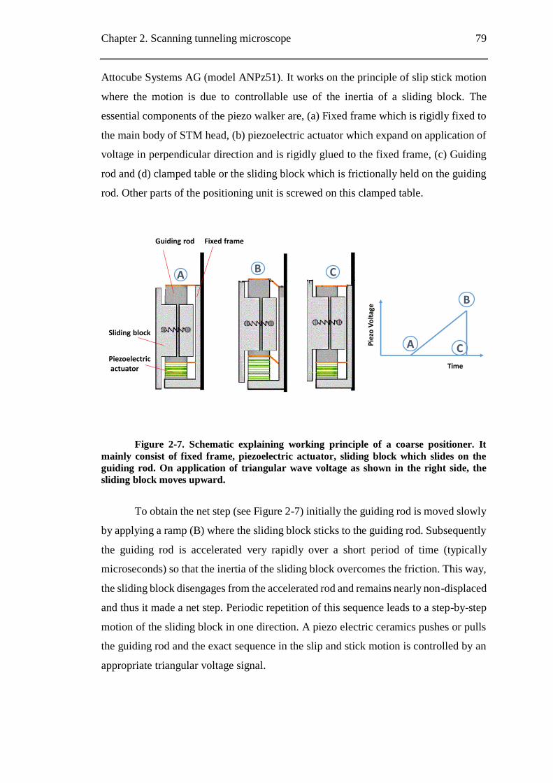
Chapter 2. Scanning tunneling microscope 79
Attocube Systems AG (model ANPz51). It works on the principle of slip stick motion
where the motion is due to controllable use of the inertia of a sliding block. The
essential components of the piezo walker are, (a) Fixed frame which is rigidly fixed to
the main body of STM head, (b) piezoelectric actuator which expand on application of
voltage in perpendicular direction and is rigidly glued to the fixed frame, (c) Guiding
rod and (d) clamped table or the sliding block which is frictionally held on the guiding
rod. Other parts of the positioning unit is screwed on this clamped table.
TimeP
iezo
Vo
ltag
e
A
B
C
AB C
Guiding rod
Piezoelectricactuator
Fixed frame
Sliding block
Figure 2-7. Schematic explaining working principle of a coarse positioner. It
mainly consist of fixed frame, piezoelectric actuator, sliding block which slides on the
guiding rod. On application of triangular wave voltage as shown in the right side, the
sliding block moves upward.
To obtain the net step (see Figure 2-7) initially the guiding rod is moved slowly
by applying a ramp (B) where the sliding block sticks to the guiding rod. Subsequently
the guiding rod is accelerated very rapidly over a short period of time (typically
microseconds) so that the inertia of the sliding block overcomes the friction. This way,
the sliding block disengages from the accelerated rod and remains nearly non-displaced
and thus it made a net step. Periodic repetition of this sequence leads to a step-by-step
motion of the sliding block in one direction. A piezo electric ceramics pushes or pulls
the guiding rod and the exact sequence in the slip and stick motion is controlled by an
appropriate triangular voltage signal.
80 Chapter 2. Scanning tunneling microscope
Piezoelectric tube
A piezoelectric tube scanner normally consists of a thin-walled cylindrical tube
of a piezoelectric material with a thin coating of gold, silver or nickel in its inner and
outer walls, (see Figure 2-8). The copper coating on the inner and outer walls of the
piezoelectric tube acts as the scanner electrodes. The outer electrode is axially quartered
into four equal sections. A pair of the opposite sections of the quartered electrode is
referred to as the X, ‒X electrodes and other pair as Y, ‒Y electrodes.
Figure 2-8. (a) Schematic sketch of the operation of the piezo tube scanner. (b-c)
For our case when a positive voltage is applied to all the four quadrants, the tube contract
in z direction while with negative voltages, it extends. (d) When opposite polarity voltages
are applied to X,‒X (or Y,‒Y) then the tube deforms laterally to produce along X (Y)
direction.
When a voltage is applied between inner electrode and one outer electrode, the
material between the electrodes stretches/contracts in the tube's longitudinal direction.
By applying the same voltage (for our case negative voltage) to all four outer electrodes,
the whole tube can be stretched, for Z tracking (see Figure 2-8). The tube can also be
bent to produce lateral deformation by applying some voltage to one outer segment
only and optionally the opposite voltage to the opposing electrode segment, for
symmetrical deformation (see Figure 2-8(d)). Thus by controlled application of various
voltages the tip can be positioned to very fined position. Total extension or lateral
deformation is given by following formulae38,

Chapter 2. Scanning tunneling microscope 81
∆𝑍 =𝑑31𝑉𝐿
𝑡
(2.16)
∆𝑋 = ∆𝑌 =0.9 𝑑31𝑉𝐿
2
𝑑𝑚𝑡
where d31 = Piezoelectric strain constant,
V = applied voltage,
L = Length of the electrode,
dm = mean diameter of the tube, (OD+ID)/2,
t = thickness of the tube.
Mechanical Description of the STM head
The outer body is made of single piece of gold plated oxygen free high
conductivity (OHFC) Copper (see Figure 2-9). The sample holder, coming from the top
Sample holder Tip
Tip holder
Piezo electric tube
Coarse positioner
Macor
Cu housing forsample holder
PCB
Cu shielding can
Steel studs
Figure 2-9. 3D view of the STM head. Outer body is made of OFHC copper.
Coarse positioner is fixed to the body at the bottom plate and it carries scanning unit on
the top. Sample holder can be inserted from the top in the Cu housing. PCB mounted on
the three sides serves as a connecting stage for electrical connections.
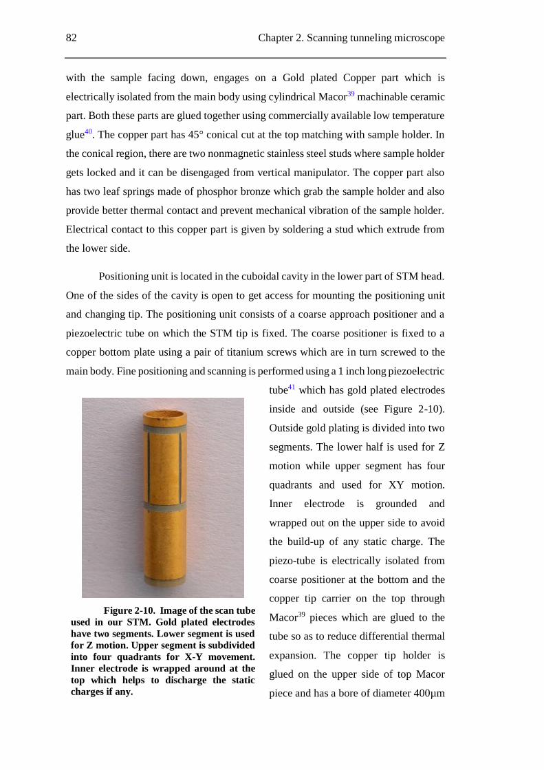
82 Chapter 2. Scanning tunneling microscope
with the sample facing down, engages on a Gold plated Copper part which is
electrically isolated from the main body using cylindrical Macor39 machinable ceramic
part. Both these parts are glued together using commercially available low temperature
glue40. The copper part has 45° conical cut at the top matching with sample holder. In
the conical region, there are two nonmagnetic stainless steel studs where sample holder
gets locked and it can be disengaged from vertical manipulator. The copper part also
has two leaf springs made of phosphor bronze which grab the sample holder and also
provide better thermal contact and prevent mechanical vibration of the sample holder.
Electrical contact to this copper part is given by soldering a stud which extrude from
the lower side.
Positioning unit is located in the cuboidal cavity in the lower part of STM head.
One of the sides of the cavity is open to get access for mounting the positioning unit
and changing tip. The positioning unit consists of a coarse approach positioner and a
piezoelectric tube on which the STM tip is fixed. The coarse positioner is fixed to a
copper bottom plate using a pair of titanium screws which are in turn screwed to the
main body. Fine positioning and scanning is performed using a 1 inch long piezoelectric
tube41 which has gold plated electrodes
inside and outside (see Figure 2-10).
Outside gold plating is divided into two
segments. The lower half is used for Z
motion while upper segment has four
quadrants and used for XY motion.
Inner electrode is grounded and
wrapped out on the upper side to avoid
the build-up of any static charge. The
piezo-tube is electrically isolated from
coarse positioner at the bottom and the
copper tip carrier on the top through
Macor39 pieces which are glued to the
tube so as to reduce differential thermal
expansion. The copper tip holder is
glued on the upper side of top Macor
piece and has a bore of diameter 400µm
Figure 2-10. Image of the scan tube
used in our STM. Gold plated electrodes
have two segments. Lower segment is used
for Z motion. Upper segment is subdivided
into four quadrants for X-Y movement.
Inner electrode is wrapped around at the
top which helps to discharge the static
charges if any.
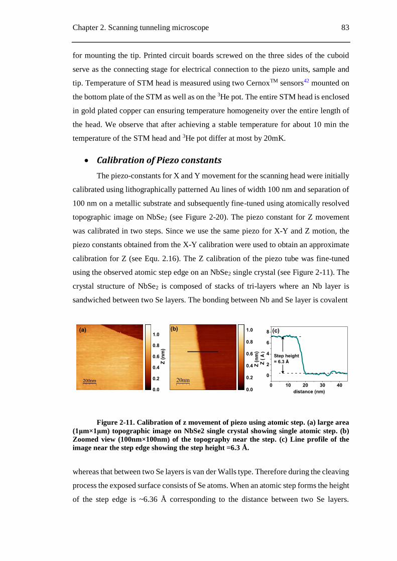
Chapter 2. Scanning tunneling microscope 83
for mounting the tip. Printed circuit boards screwed on the three sides of the cuboid
serve as the connecting stage for electrical connection to the piezo units, sample and
tip. Temperature of STM head is measured using two CernoxTM sensors42 mounted on
the bottom plate of the STM as well as on the 3He pot. The entire STM head is enclosed
in gold plated copper can ensuring temperature homogeneity over the entire length of
the head. We observe that after achieving a stable temperature for about 10 min the
temperature of the STM head and 3He pot differ at most by 20mK.
Calibration of Piezo constants
The piezo-constants for X and Y movement for the scanning head were initially
calibrated using lithographically patterned Au lines of width 100 nm and separation of
100 nm on a metallic substrate and subsequently fine-tuned using atomically resolved
topographic image on NbSe2 (see Figure 2-20). The piezo constant for Z movement
was calibrated in two steps. Since we use the same piezo for X-Y and Z motion, the
piezo constants obtained from the X-Y calibration were used to obtain an approximate
calibration for Z (see Equ. 2.16). The Z calibration of the piezo tube was fine-tuned
using the observed atomic step edge on an NbSe2 single crystal (see Figure 2-11). The
crystal structure of NbSe2 is composed of stacks of tri-layers where an Nb layer is
sandwiched between two Se layers. The bonding between Nb and Se layer is covalent
0.0
0.2
0.4
0.6
0.8
1.0
Z (
nm
)
(a) (b)
0 10 20 30 40
0
2
4
6
8
distance (nm)
Z (
Å )
Step height
= 6.3 Å
0.0
0.2
0.4
0.6
0.8
1.0 (c)
Z
(n
m)
Figure 2-11. Calibration of z movement of piezo using atomic step. (a) large area
(1μm×1μm) topographic image on NbSe2 single crystal showing single atomic step. (b)
Zoomed view (100nm×100nm) of the topography near the step. (c) Line profile of the
image near the step edge showing the step height =6.3 Å.
whereas that between two Se layers is van der Walls type. Therefore during the cleaving
process the exposed surface consists of Se atoms. When an atomic step forms the height
of the step edge is ~6.36 Å corresponding to the distance between two Se layers.
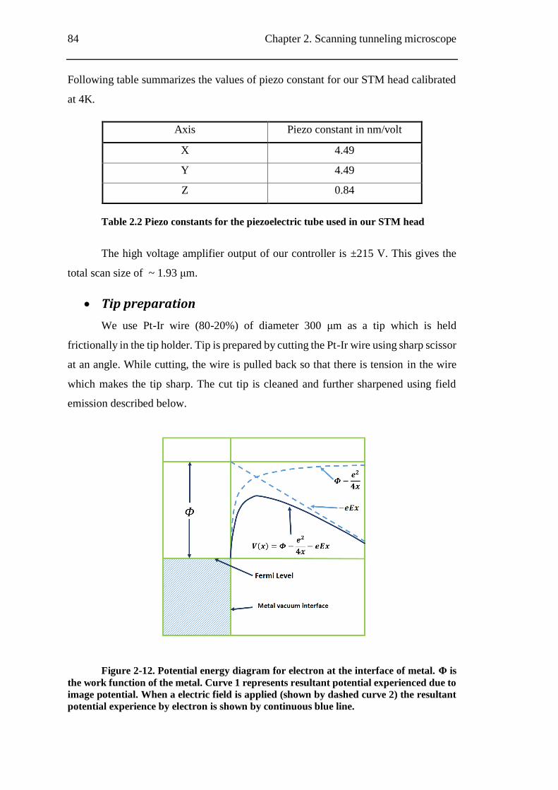
84 Chapter 2. Scanning tunneling microscope
Following table summarizes the values of piezo constant for our STM head calibrated
at 4K.
Axis Piezo constant in nm/volt
X 4.49
Y 4.49
Z 0.84
Table 2.2 Piezo constants for the piezoelectric tube used in our STM head
The high voltage amplifier output of our controller is ±215 V. This gives the
total scan size of ~ 1.93 μm.
Tip preparation
We use Pt-Ir wire (80-20%) of diameter 300 μm as a tip which is held
frictionally in the tip holder. Tip is prepared by cutting the Pt-Ir wire using sharp scissor
at an angle. While cutting, the wire is pulled back so that there is tension in the wire
which makes the tip sharp. The cut tip is cleaned and further sharpened using field
emission described below.
Figure 2-12. Potential energy diagram for electron at the interface of metal. Φ is
the work function of the metal. Curve 1 represents resultant potential experienced due to
image potential. When a electric field is applied (shown by dashed curve 2) the resultant
potential experience by electron is shown by continuous blue line.
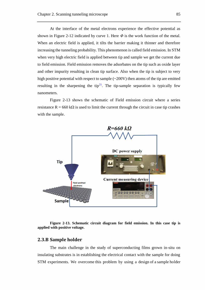
Chapter 2. Scanning tunneling microscope 85
At the interface of the metal electrons experience the effective potential as
shown in Figure 2-12 indicated by curve 1. Here Φ is the work function of the metal.
When an electric field is applied, it tilts the barrier making it thinner and therefore
increasing the tunneling probability. This phenomenon is called field emission. In STM
when very high electric field is applied between tip and sample we get the current due
to field emission. Field emission removes the adsorbates on the tip such as oxide layer
and other impurity resulting in clean tip surface. Also when the tip is subject to very
high positive potential with respect to sample (~200V) then atoms of the tip are emitted
resulting in the sharpening the tip21. The tip-sample separation is typically few
nanometers.
Figure 2-13 shows the schematic of Field emission circuit where a series
resistance R = 660 kΩ is used to limit the current through the circuit in case tip crashes
with the sample.
Figure 2-13. Schematic circuit diagram for field emission. In this case tip is
applied with positive voltage.
2.3.B Sample holder
The main challenge in the study of superconducting films grown in-situ on
insulating substrates is in establishing the electrical contact with the sample for doing
STM experiments. We overcome this problem by using a design of a sample holder
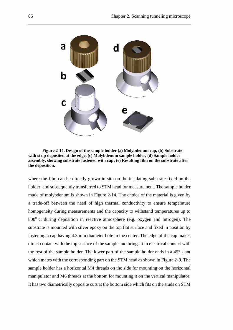
86 Chapter 2. Scanning tunneling microscope
Figure 2-14. Design of the sample holder (a) Molybdenum cap, (b) Substrate
with strip deposited at the edge, (c) Molybdenum sample holder, (d) Sample holder
assembly, showing substrate fastened with cap; (e) Resulting film on the substrate after
the deposition.
where the film can be directly grown in-situ on the insulating substrate fixed on the
holder, and subsequently transferred to STM head for measurement. The sample holder
made of molybdenum is shown in Figure 2-14. The choice of the material is given by
a trade-off between the need of high thermal conductivity to ensure temperature
homogeneity during measurements and the capacity to withstand temperatures up to
8000 C during deposition in reactive atmosphere (e.g. oxygen and nitrogen). The
substrate is mounted with silver epoxy on the top flat surface and fixed in position by
fastening a cap having 4.3 mm diameter hole in the center. The edge of the cap makes
direct contact with the top surface of the sample and brings it in electrical contact with
the rest of the sample holder. The lower part of the sample holder ends in a 45° slant
which mates with the corresponding part on the STM head as shown in Figure 2-9. The
sample holder has a horizontal M4 threads on the side for mounting on the horizontal
manipulator and M6 threads at the bottom for mounting it on the vertical manipulator.
It has two diametrically opposite cuts at the bottom side which fits on the studs on STM
Chapter 2. Scanning tunneling microscope 87
head and locks the circular movement while disengaging the sample holder from the
vertical manipulator after the sample is mounted on the STM head.
For STM measurements on films grown on insulating substrates, first two
contact strips are deposited ex-situ on two edges of the substrate as shown in Figure 2-
14 (b). The width of the strips is adjusted such that when the substrate with contact pads
is mounted on the sample holder, a small portion of the strip on either side is exposed
through the hole in the cap (Figure 2-14 (d)). When the superconducting film is
deposited on the substrate in the in-situ chamber, the edge of the film is in contact with
the strip and is therefore electrically connected to the entire sample holder. In principle,
the strips could be made of any material that can withstand the deposition temperature
of the superconducting film. However, in most cases we found it convenient to make
the strips of the same material as the material under study. Since our STM head is
symmetric, the tip engages at the center of the sample which ensures tip to strip distance
~ 1 mm. This is much larger than the length over which we would expect
superconducting proximity effects from the contact pads to play any role in the
measurements.
For the study of single crystals a single piece sample holder of similar shape
without the cap is used. The crystal is mounted on the flat surface using a two
component conducting silver epoxy43. Depending on the hardness, the crystal is cleaved
in vacuum (in the load lock cross) alternatively by gluing a small rod on the surface
using the same silver epoxy and hitting it with a hammer or by gluing a tape on the
surface and pulling the tape using one of the manipulators.
2.3.C Sample Preparation chamber
The sample preparation chamber, fitted with a turbo molecular pump and with
a base pressure ~ 1×10⁻⁷ mbar, is located on the top of table and is connected to load
lock through a gate valve (Figure 2-15). The chamber consists of two magnetron
sputtering guns facing down at an angle, to the substrate heater. The confocal
arrangement of guns allows for co-sputtering. The substrate heater consists of a
resistive heating element made of a patterned molybdenum plate. Sample holder is
inserted using the horizontal manipulator in the chamber through the load-lock and held
above the heater. It is heated radiatively and its temperature is measured using thermo-
couple (PT100) located inside, at the tip of the horizontal manipulator. In addition, the
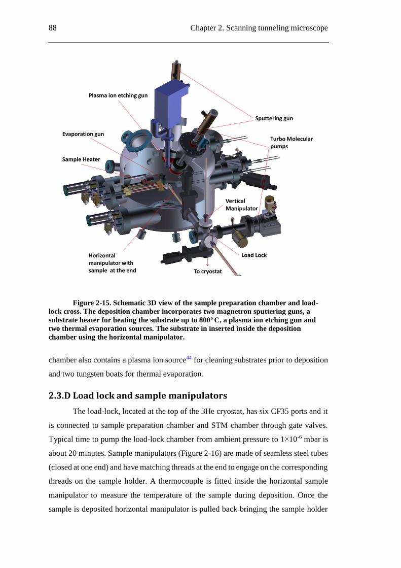
88 Chapter 2. Scanning tunneling microscope
Sputtering gun
Plasma ion etching gun
Evaporation gun
Sample Heater
Horizontal manipulator with sample at the end
Load Lock
Turbo Molecularpumps
To cryostat
Vertical Manipulator
Figure 2-15. Schematic 3D view of the sample preparation chamber and load-
lock cross. The deposition chamber incorporates two magnetron sputtering guns, a
substrate heater for heating the substrate up to 800º C, a plasma ion etching gun and
two thermal evaporation sources. The substrate in inserted inside the deposition
chamber using the horizontal manipulator.
chamber also contains a plasma ion source44 for cleaning substrates prior to deposition
and two tungsten boats for thermal evaporation.
2.3.D Load lock and sample manipulators
The load-lock, located at the top of the 3He cryostat, has six CF35 ports and it
is connected to sample preparation chamber and STM chamber through gate valves.
Typical time to pump the load-lock chamber from ambient pressure to 1×10⁻⁶ mbar is
about 20 minutes. Sample manipulators (Figure 2-16) are made of seamless steel tubes
(closed at one end) and have matching threads at the end to engage on the corresponding
threads on the sample holder. A thermocouple is fitted inside the horizontal sample
manipulator to measure the temperature of the sample during deposition. Once the
sample is deposited horizontal manipulator is pulled back bringing the sample holder

Chapter 2. Scanning tunneling microscope 89
in the cross, and the sample holder is transferred to vertical manipulator and inserted
into the STM head.
Sample holder
To pump
Thermocouple
M4 threading
Wilson seal
CF 35 flange
Figure 2-16. Design of the horizontal sample manipulator with in-built
thermocouple for measuring the temperature during sample deposition. A differential
pumping arrangement between two Wilson seals is used to remove any leaked gas during
movement. The end of the manipulator is made transparent to show the position of the
thermocouple. The vertical manipulator is similar in construction but does not have the
thermocouple.
2.3.E 3He Cryostat
The low temperature stage consists of an internally fitted charcoal sorption
pump based 3He cryostat from Janis Research Company45 (Figure 2-17). The cryostat
essentially consists of variable temperature insert and a liquid helium Dewar with
superconducting magnet.
Variable temperature insert
We use a custom designed insert which consists of annular shaped sorption
pump, 1K pot and 3He pot which give us direct line of site access from the top of the
cryostat to the STM head mounted below the 3He pot. To ensure thermal stability the
STM head is bolted to 3He pot using 6 screws which ensures good thermal contact
between the two. To prevent radiative heating, a radiation plug is inserted in the cryostat
after loading the sample using the same vertical manipulator as the one used to insert
the sample. The radiation plug (not shown) sits just above the STM head. The 3He pot
and sorption pump are fitted with resistive heaters. Top flange have many feedthroughs
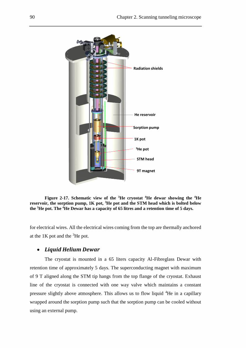
90 Chapter 2. Scanning tunneling microscope
Radiation shields
He reservoir
Sorption pump
1K pot
3He pot
STM head
9T magnet
Figure 2-17. Schematic view of the 3He cryostat 4He dewar showing the 4He
reservoir, the sorption pump, 1K pot, 3He pot and the STM head which is bolted below
the 3He pot. The 4He Dewar has a capacity of 65 litres and a retention time of 5 days.
for electrical wires. All the electrical wires coming from the top are thermally anchored
at the 1K pot and the 3He pot.
Liquid Helium Dewar
The cryostat is mounted in a 65 liters capacity Al-Fibreglass Dewar with
retention time of approximately 5 days. The superconducting magnet with maximum
of 9 T aligned along the STM tip hangs from the top flange of the cryostat. Exhaust
line of the cryostat is connected with one way valve which maintains a constant
pressure slightly above atmosphere. This allows us to flow liquid 4He in a capillary
wrapped around the sorption pump such that the sorption pump can be cooled without
using an external pump.
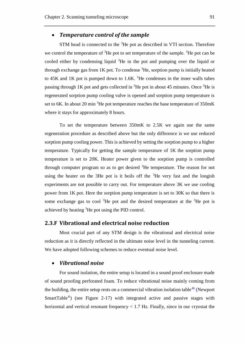
Chapter 2. Scanning tunneling microscope 91
Temperature control of the sample
STM head is connected to the 3He pot as described in VTI section. Therefore
we control the temperature of 3He pot to set temperature of the sample. 3He pot can be
cooled either by condensing liquid 3He in the pot and pumping over the liquid or
through exchange gas from 1K pot. To condense 3He, sorption pump is initially heated
to 45K and 1K pot is pumped down to 1.6K. 3He condenses in the inner walls tubes
passing through 1K pot and gets collected in 3He pot in about 45 minutes. Once 3He is
regenerated sorption pump cooling valve is opened and sorption pump temperature is
set to 6K. In about 20 min 3He pot temperature reaches the base temperature of 350mK
where it stays for approximately 8 hours.
To set the temperature between 350mK to 2.5K we again use the same
regeneration procedure as described above but the only difference is we use reduced
sorption pump cooling power. This is achieved by setting the sorption pump to a higher
temperature. Typically for getting the sample temperature of 1K the sorption pump
temperature is set to 20K. Heater power given to the sorption pump is controlled
through computer program so as to get desired 3He temperature. The reason for not
using the heater on the 3He pot is it boils off the 3He very fast and the longish
experiments are not possible to carry out. For temperature above 3K we use cooling
power from 1K pot. Here the sorption pump temperature is set to 30K so that there is
some exchange gas to cool 3He pot and the desired temperature at the 3He pot is
achieved by heating 3He pot using the PID control.
2.3.F Vibrational and electrical noise reduction
Most crucial part of any STM design is the vibrational and electrical noise
reduction as it is directly reflected in the ultimate noise level in the tunneling current.
We have adopted following schemes to reduce eventual noise level.
Vibrational noise
For sound isolation, the entire setup is located in a sound proof enclosure made
of sound proofing perforated foam. To reduce vibrational noise mainly coming from
the building, the entire setup rests on a commercial vibration isolation table46 (Newport
SmartTable®) (see Figure 2-17) with integrated active and passive stages with
horizontal and vertical resonant frequency < 1.7 Hz. Finally, since in our cryostat the
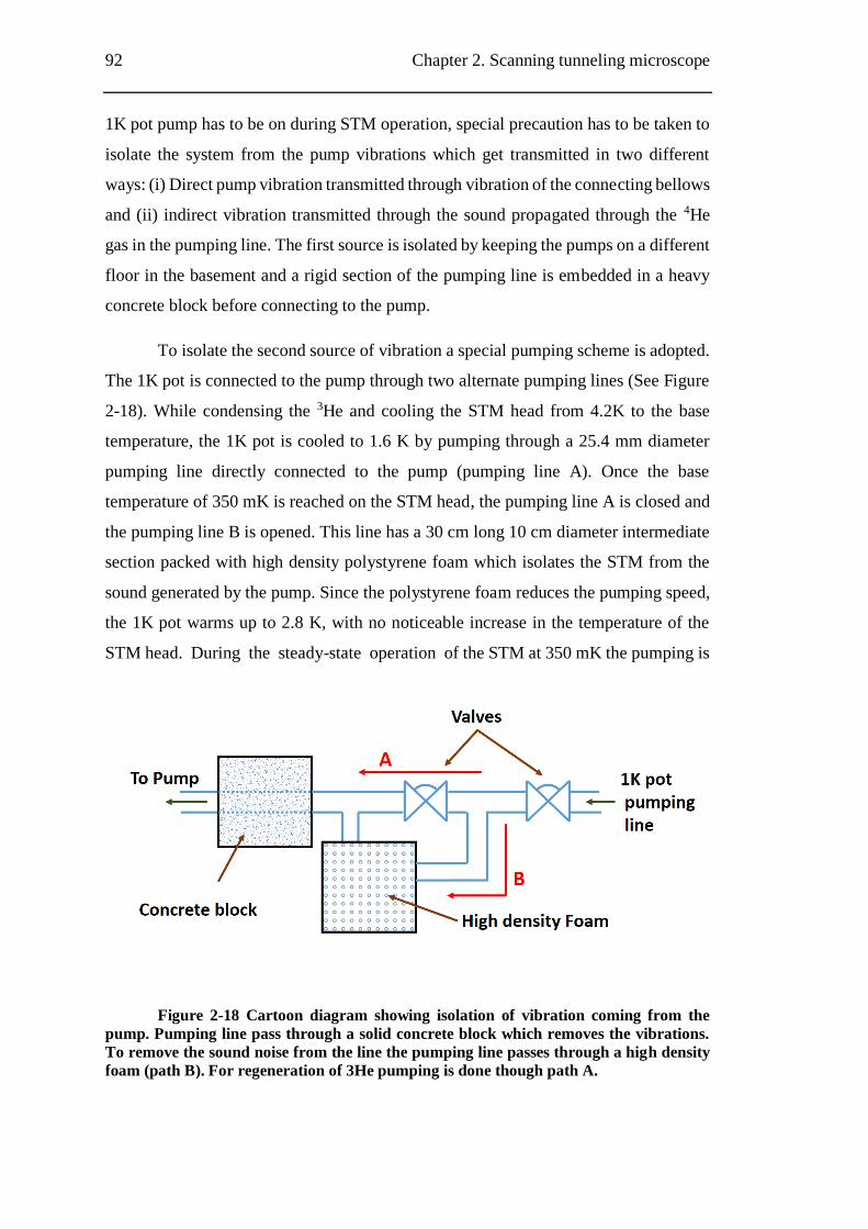
92 Chapter 2. Scanning tunneling microscope
1K pot pump has to be on during STM operation, special precaution has to be taken to
isolate the system from the pump vibrations which get transmitted in two different
ways: (i) Direct pump vibration transmitted through vibration of the connecting bellows
and (ii) indirect vibration transmitted through the sound propagated through the 4He
gas in the pumping line. The first source is isolated by keeping the pumps on a different
floor in the basement and a rigid section of the pumping line is embedded in a heavy
concrete block before connecting to the pump.
To isolate the second source of vibration a special pumping scheme is adopted.
The 1K pot is connected to the pump through two alternate pumping lines (See Figure
2-18). While condensing the 3He and cooling the STM head from 4.2K to the base
temperature, the 1K pot is cooled to 1.6 K by pumping through a 25.4 mm diameter
pumping line directly connected to the pump (pumping line A). Once the base
temperature of 350 mK is reached on the STM head, the pumping line A is closed and
the pumping line B is opened. This line has a 30 cm long 10 cm diameter intermediate
section packed with high density polystyrene foam which isolates the STM from the
sound generated by the pump. Since the polystyrene foam reduces the pumping speed,
the 1K pot warms up to 2.8 K, with no noticeable increase in the temperature of the
STM head. During the steady-state operation of the STM at 350 mK the pumping is
Figure 2-18 Cartoon diagram showing isolation of vibration coming from the
pump. Pumping line pass through a solid concrete block which removes the vibrations.
To remove the sound noise from the line the pumping line passes through a high density
foam (path B). For regeneration of 3He pumping is done though path A.
Chapter 2. Scanning tunneling microscope 93
0 25 50 75 10010
0
101
102
103
0 25 50 75 100
101
102
103
0 50 100 150 200
101
102
103
Ve
locit
y (
nm
s-1 H
z-1
/2)
Frequency (Hz)
1K pot pumping on
1K pot pumping off
cu
rren
t S
D (
fA H
z-1
/2)
Frequency (Hz)
Tip engaged (Feedback off)
Tip engaged (Feedback on)
Tip retracted
Z (
fm H
z-1
/2)
Frequency (Hz)
Figure 2-19. Noise characterization (a) Spectral density of the velocity vs.
frequency on the top of the cryostat measured using an accelerometer. The spectral
densities with and without the 1K pot pump on are nearly identical. (b) Spectral density
of the tunneling current with the tip out of tunneling range, within tunneling range with
feedback on and with feedback off. (c) Spectral density of Z height signal with feedback
on. Measurements in (b) and (c) were performed at 350 mK on a NbSe2 single crystal
with tunneling current set to 50 pA and bias voltage to 20 mV.
further reduced by partially closing a valve to keep the 1K pot at a constant temperature
of ~ 3.5K. While operating in this mode we do not observe any difference in vibration
level on the top of the cryostat with the 1K pot pump on or off.
Electrical noise
To reduce the electrical noise coming from the 50Hz line signal, ground
connection of all instruments, table and Dewar are made to a separate master ground.
RF noise is further reduced by introducing 10 MHz low pass filter before each
94 Chapter 2. Scanning tunneling microscope
connection that goes into the STM. The tunneling current is detected using a Femto
DLPCA-200 current amplifier placed at the top of the cryostat with gain of 109 V/A.
While the bandwidth of the DLCPA-200 amplifier is 500 kHz, the measurement
bandwidth is set digitally restricted to 2.5 kHz in the R9 SPM controller.
Characterization of noise
In our system we have low Z-height and current noise that allows us to get very
good signal to noise ratio in spectroscopic measurements as discussed in next sections.
Figure 2-19 (a) shows the vibration noise spectrum recorded using the accelerometer
on the table while the 1K pot pumping line is on and off. The two profiles show
practically no difference in the vibration levels. The final test of isolation performance
is obtained from the spectral density (SD) in the current and Z-height signals. We
recorded these signals at 350 mK in actual operating condition. Figure 2-19(b) shows
the SD of the current (i) when the tip is out of tunneling range (background noise of the
electronics), (ii) at a fixed tunneling current with feedback on condition, and (iii) after
switching off the feedback for 5 s. The SD with tip out of tunneling range is below 300
fA Hz-1/2. At fixed tunneling current (feedback on) additional peaks appear in the SD
at 25.5 Hz and 91.5 Hz but the peak signal is only marginally larger than 300 fA Hz-1/2.
Even after switching off the feedback the peak signal is less than 1 pA Hz-1/2. Similarly,
the Z-height SD at fixed tunneling current with feedback on (Figure 2-19(c)) is less
than 2 pm Hz-1/2 at all frequencies and less than 50 fm Hz-1/2 above 150 Hz.
2.4 Experimental Methods and results
In this section we discuss experimental techniques and the scheme of
experiments we use in this thesis. In our STM for applying bias and tunneling current
measurements we use the same master ground. We can measure the tunneling current
as a function of X, Y, Z and V (bias).
2.4.A Topography
Topography is the most common mode STM measurement employed all
around. To acquire topographic image the tip is raster scanned across the surface of the
sample in constant current mode and the Z variations are recorded as a function of
position, Z(X, Y). As seen in section 2.2.A constant current topography represents
contours of constant electronic density of states at the surface.
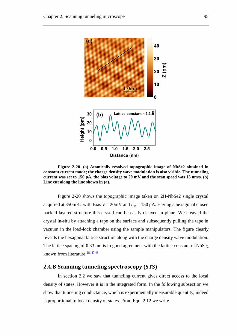
Chapter 2. Scanning tunneling microscope 95
0.0 0.5 1.0 1.5 2.0 2.5
0
10
20
30
0
10
20
30
40
Heig
ht
(pm
)
Distance (nm)
Lattice constant = 3.3 Å (b)
Z (
pm
)
(a)
Figure 2-20. (a) Atomically resolved topographic image of NbSe2 obtained in
constant current mode; the charge density wave modulation is also visible. The tunneling
current was set to 150 pA, the bias voltage to 20 mV and the scan speed was 13 nm/s. (b)
Line cut along the line shown in (a).
Figure 2-20 shows the topographic image taken on 2H-NbSe2 single crystal
acquired at 350mK. with Bias V = 20mV and Iset = 150 pA. Having a hexagonal closed
packed layered structure this crystal can be easily cleaved in-plane. We cleaved the
crystal in-situ by attaching a tape on the surface and subsequently pulling the tape in
vacuum in the load-lock chamber using the sample manipulators. The figure clearly
reveals the hexagonal lattice structure along with the charge density wave modulation.
The lattice spacing of 0.33 nm is in good agreement with the lattice constant of NbSe2
known from literature.28, 47,48
2.4.B Scanning tunneling spectroscopy (STS)
In section 2.2 we saw that tunneling current gives direct access to the local
density of states. However it is in the integrated form. In the following subsection we
show that tunneling conductance, which is experimentally measurable quantity, indeed
is proportional to local density of states. From Equ. 2.12 we write
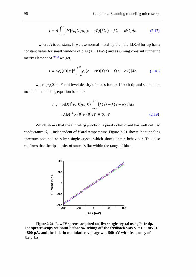
96 Chapter 2. Scanning tunneling microscope
𝐼 = 𝐴∫ |𝑀|2𝜌𝑡(휀)𝜌𝑠(휀 − 𝑒𝑉)[𝑓(휀) − 𝑓(휀 − 𝑒𝑉)]𝑑휀∞
−∞
(2.17)
where A is constant. If we use normal metal tip then the LDOS for tip has a
constant value for small window of bias (< 100mV) and assuming constant tunneling
matrix element M 49,52 we get,
𝐼 = 𝐴𝜌𝑡(0)|𝑀|2∫ 𝜌𝑠(휀 − 𝑒𝑉)[𝑓(휀) − 𝑓(휀 − 𝑒𝑉)]𝑑휀
∞
−∞
(2.18)
where 𝜌𝑡(0) is Fermi level density of states for tip. If both tip and sample are
metal then tunneling equation becomes,
𝐼𝑛𝑛 = 𝐴|𝑀|2𝜌𝑡(0)𝜌𝑠(0)∫ [𝑓(휀) − 𝑓(휀 − 𝑒𝑉)]𝑑휀
∞
−∞
= 𝐴|𝑀|2𝜌𝑡(0)𝜌𝑠(0)𝑒𝑉 ≡ 𝐺𝑛𝑛𝑉 (2.19)
Which shows that the tunneling junction is purely ohmic and has well defined
conductance 𝐺𝑛𝑛, independent of V and temperature. Figure 2-21 shows the tunneling
spectrum obtained on silver single crystal which shows ohmic behaviour. This also
confirms that the tip density of states is flat within the range of bias.
-100 -50 0 50 100-600
-300
0
300
600
Cu
rren
t in
pA
Bias (mV)
Figure 2-21. Raw IV spectra acquired on silver single crystal using Pt-Ir tip.
The spectroscopy set point before switching off the feedback was V = 100 mV, I
= 500 pA, and the lock-in modulation voltage was 500 V with frequency of
419.3 Hz.
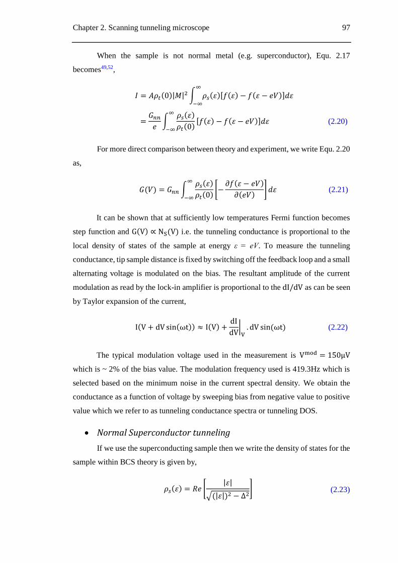
Chapter 2. Scanning tunneling microscope 97
When the sample is not normal metal (e.g. superconductor), Equ. 2.17
becomes49,52,
𝐼 = 𝐴𝜌𝑡(0)|𝑀|2∫ 𝜌𝑠(휀)[𝑓(휀) − 𝑓(휀 − 𝑒𝑉)]𝑑휀
∞
−∞
=𝐺𝑛𝑛𝑒∫
𝜌𝑠(휀)
𝜌𝑡(0)[𝑓(휀) − 𝑓(휀 − 𝑒𝑉)]𝑑휀
∞
−∞
(2.20)
For more direct comparison between theory and experiment, we write Equ. 2.20
as,
𝐺(𝑉) = 𝐺𝑛𝑛∫𝜌𝑠(휀)
𝜌𝑡(0)[−𝜕𝑓(휀 − 𝑒𝑉)
𝜕(𝑒𝑉)]𝑑휀
∞
−∞
(2.21)
It can be shown that at sufficiently low temperatures Fermi function becomes
step function and G(V) ∝ NS(V) i.e. the tunneling conductance is proportional to the
local density of states of the sample at energy ε = eV. To measure the tunneling
conductance, tip sample distance is fixed by switching off the feedback loop and a small
alternating voltage is modulated on the bias. The resultant amplitude of the current
modulation as read by the lock-in amplifier is proportional to the dI/dV as can be seen
by Taylor expansion of the current,
I(V + dV sin(ωt)) ≈ I(V) +dI
dV|V. dV sin(ωt) (2.22)
The typical modulation voltage used in the measurement is Vmod = 150μV
which is ~ 2% of the bias value. The modulation frequency used is 419.3Hz which is
selected based on the minimum noise in the current spectral density. We obtain the
conductance as a function of voltage by sweeping bias from negative value to positive
value which we refer to as tunneling conductance spectra or tunneling DOS.
Normal Superconductor tunneling
If we use the superconducting sample then we write the density of states for the
sample within BCS theory is given by,
𝜌𝑠(휀) = 𝑅𝑒 [|휀|
√(|휀|)2 − Δ2] (2.23)
98 Chapter 2. Scanning tunneling microscope
-4 -2 0 2 40
1
2
G(V
)/G
(5 m
V)
V(mV)
data
BCS fit
meV
Figure 2-22. Tunneling spectroscopy on Pb single crystal acquired with Pt-
Ir tip at 500mK (red circle) along with BCS fit with fit temperature =500mK. The
spectrum is averaged over 10 voltage sweeps at the same point. The spectroscopy
set point before switching off the feedback was V = 6 mV, I = 500 pA, and the lock-
in modulation voltage was 150 V with frequency of 419.3 Hz.
Figure 2-22 shows the typical spectrum acquired at 500mK at a single point on
polished Pb single crystal. The spectrum shows two distinct peaks called as coherence
peaks and a dip close to Fermi level indicating the gap. Figure 2-22 also shows the fit
using BCS density of states (Equ. 2.20 and 2.22). We have taken into account
broadening due to the finite modulation voltage which is used for lock-in measurements
by doing adjacent averaging of points in the theoretical curve over a sliding voltage
range of 150 V. BCS fit gives an energy gap Δ=1.3 meV which is in good agreement50
with reported values of the energy gap in Pb.
2.4.C Linescan
In the previous section we saw the spectroscopy at single point on the surface
of the sample. Since we have (X, Y) control we can acquire the density of states
anywhere on the surface within the scan range. Some samples with no impurity may
have uniform DOS but for some interesting samples tunneling DOS may be
inhomogeneous. To study the inhomogeneity we can measure the conductance spectra
along a line at equispaced interval. We call this data as a linescan.
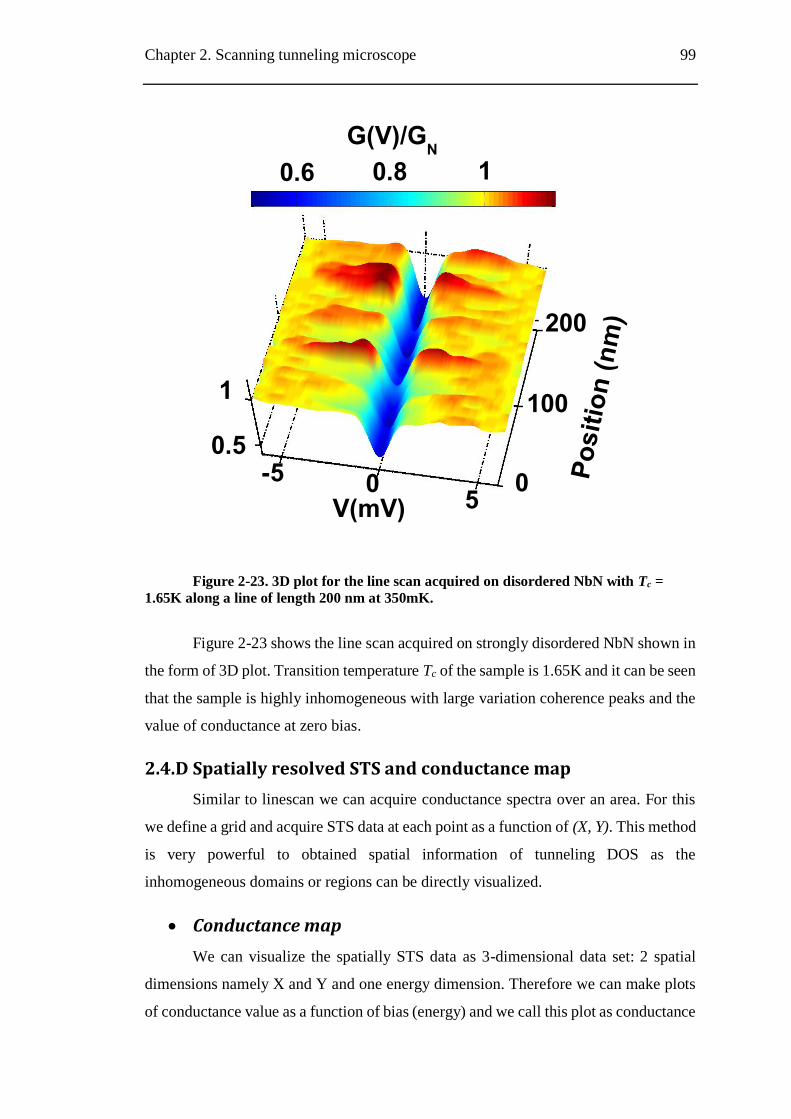
Chapter 2. Scanning tunneling microscope 99
V(mV)
0.6 0.8 1
0.5
G(V)/GN
Po
sit
ion
(n
m)
0
100
200
0-55
1
Figure 2-23. 3D plot for the line scan acquired on disordered NbN with Tc =
1.65K along a line of length 200 nm at 350mK.
Figure 2-23 shows the line scan acquired on strongly disordered NbN shown in
the form of 3D plot. Transition temperature Tc of the sample is 1.65K and it can be seen
that the sample is highly inhomogeneous with large variation coherence peaks and the
value of conductance at zero bias.
2.4.D Spatially resolved STS and conductance map
Similar to linescan we can acquire conductance spectra over an area. For this
we define a grid and acquire STS data at each point as a function of (X, Y). This method
is very powerful to obtained spatial information of tunneling DOS as the
inhomogeneous domains or regions can be directly visualized.
Conductance map
We can visualize the spatially STS data as 3-dimensional data set: 2 spatial
dimensions namely X and Y and one energy dimension. Therefore we can make plots
of conductance value as a function of bias (energy) and we call this plot as conductance
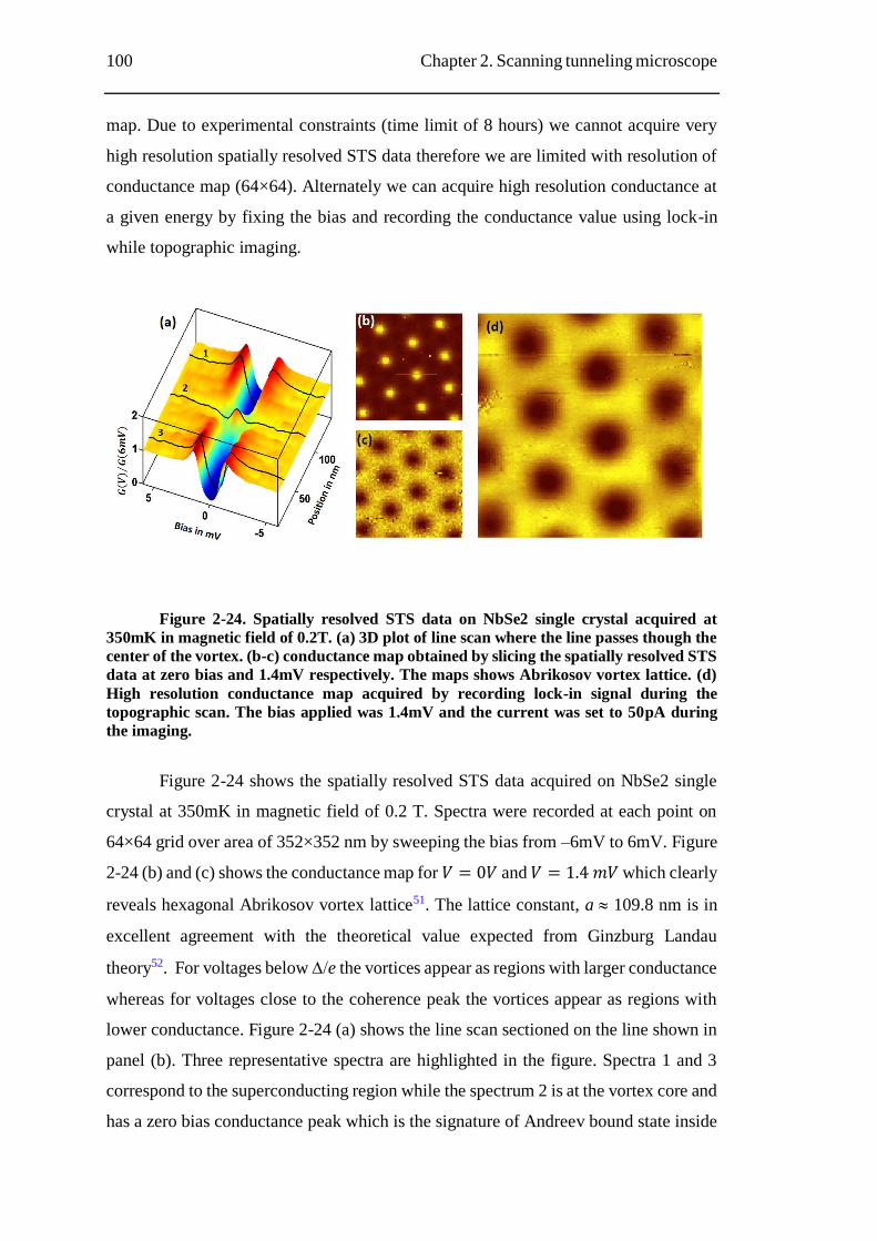
100 Chapter 2. Scanning tunneling microscope
map. Due to experimental constraints (time limit of 8 hours) we cannot acquire very
high resolution spatially resolved STS data therefore we are limited with resolution of
conductance map (64×64). Alternately we can acquire high resolution conductance at
a given energy by fixing the bias and recording the conductance value using lock-in
while topographic imaging.
Figure 2-24. Spatially resolved STS data on NbSe2 single crystal acquired at
350mK in magnetic field of 0.2T. (a) 3D plot of line scan where the line passes though the
center of the vortex. (b-c) conductance map obtained by slicing the spatially resolved STS
data at zero bias and 1.4mV respectively. The maps shows Abrikosov vortex lattice. (d)
High resolution conductance map acquired by recording lock-in signal during the
topographic scan. The bias applied was 1.4mV and the current was set to 50pA during
the imaging.
Figure 2-24 shows the spatially resolved STS data acquired on NbSe2 single
crystal at 350mK in magnetic field of 0.2 T. Spectra were recorded at each point on
64×64 grid over area of 352×352 nm by sweeping the bias from ‒6mV to 6mV. Figure
2-24 (b) and (c) shows the conductance map for 𝑉 = 0𝑉 and 𝑉 = 1.4 𝑚𝑉 which clearly
reveals hexagonal Abrikosov vortex lattice51. The lattice constant, a 109.8 nm is in
excellent agreement with the theoretical value expected from Ginzburg Landau
theory52. For voltages below e the vortices appear as regions with larger conductance
whereas for voltages close to the coherence peak the vortices appear as regions with
lower conductance. Figure 2-24 (a) shows the line scan sectioned on the line shown in
panel (b). Three representative spectra are highlighted in the figure. Spectra 1 and 3
correspond to the superconducting region while the spectrum 2 is at the vortex core and
has a zero bias conductance peak which is the signature of Andreev bound state inside
Chapter 2. Scanning tunneling microscope 101
the vortex core53. In Figure 2-24(d) we show a high resolution (128 128) conductance
map obtained by measuring dI/dV at a fixed bias voltage of 1.4mV while scanning over
the same area.
2.5 Reference
1 G. Binnig, H. Rohrer, Ch. Gerber and E. Weibel, Tunneling through a controllable
vacuum gap, Appl. Phys. Lett. 40, 178 (1982)
2 G. Binnig, H. Rohrer, Ch. Gerber, and E. Weibel, Surface Studies by Scanning
Tunneling Microscopy, Phys. Rev. Lett. 49, 57–61 (1982)
3 G. Binnig and H. Rohrer, Scanning tunneling microscopy, Surf. Sci. 126, 236
(1983).
4 G. Binnig, H. Rohrer, Ch. Gerber, and E. Weibel, 7 × 7 Reconstruction on Si(111)
Resolved in Real Space, Phys. Rev. Lett. 50, 120–123 (1983)
5 J. A. Stroscio, D. M. Eigler, Atomic and Molecular Manipulation with the Scanning
Tunneling Microscope, Science 254, 1319 (1991).
6 M. F. Crommie, C. Lutz, and D. Eigler, Confinement of Electrons to Quantum
Corrals on a Metal Surface, Science 262, 218 (1993).
7 H. C. Manoharan, C. Lutz, and D. Eigler, Quantum mirages formed by coherent
projection of electronic structure, Nature 403, 512 (2000).
8 V. Madhavan V, W. Chen, T. Jamneala, M. F. Crommie, N. S. Wingreen, Tunneling
into a single magnetic atom: Spectroscopic evidence of the Kondo resonance. Science
280, 567 (1998).
102 Chapter 2. Scanning tunneling microscope
9 H. F. Hess, R. B. Robinson, R. C. Dynes, J. J. M. Valles, and J. V. Waszczak,
Scanning-Tunneling-Microscope Observation of the Abrikosov Flux Lattice and the
Density of States near and inside a Fluxoid, Phys. Rev. Lett. 62, 214 (1989).
10 R. Wiesendanger, Spin mapping at the nanoscale and atomic scale, Rev. Mod.
Phys. 81, 1495 (2009).
11 L. Gross, F. Mohn, N. Moll, P. Liljeroth, G. Meyer, The Chemical Structure of a
Molecule Resolved by Atomic Force Microscopy, Science 325, 1110 (2009).
12 D. G. de Oteyza, P. Gorman, Y. C. Chen, S. Wickenburg, A. Riss, D. J. Mowbray,
G. Etkin, Z. Pedramrazi, H. Z. Tsai, A. Rubio, M. F. Crommie, F. R. Fischer, Direct
imaging of covalent bond structure in single-molecule chemical reactions. Science
340, 1434–1437 (2013).
13 Claude Cohen-Tannoudji, Bernard Diu, Frank Laloe Quantum Mechanics Vol.1,
Wiley; 1st edition (January 8, 1991)
14 J. Bardeen, Tunnelling from a Many-Particle Point of View, Phys. Rev. Lett. 6, 57
(1961)
15 Giaever I. Energy Gap in Superconductors Measured by Electron Tunneling, Phys.
Rev. Lett. 5, 147–148 (1960)
16 J. Tersoff and D. R. Hamann, Theory and Application for the Scanning Tunneling
Microscope, Phys. Rev. Lett. 50, 1998–2001 (1983)
17 J. Tersoff and D. R. Hamann, Theory of the scanning tunneling microscope, Phys.
Rev. B 31, 805–813 (1985)
18 A. Baratoff, Theory of scanning tunneling microscopy - methods and
approximations, Physica B (Amsterdam) 127 (1984) 143.
19 C. Julian Chen, Tunneling matrix elements in three-dimensional space: The
derivative rule and the sum rule, Phys. Rev. B 42, 8841–8857 (1990)
20 C. Julian Chen, Origin of atomic resolution on metal surfaces in scanning tunneling
microscopy, Phys. Rev. Lett. 65, 448–451 (1990)
21 C. Julian Chen, Microscopic view of scanning tunneling microscopy, J. Vac. Sci.
Technol. A 9, 44 (1991);
Chapter 2. Scanning tunneling microscope 103
22 S. H. Pan, E. W. Hudson, and J. C. Davis, 3He refrigerator based very low
temperature scanning tunneling microscope, Rev. Sci. Instrum. 70, 1459 (1999).
23 Maximilian Assig, Markus Etzkorn, Axel Enders, Wolfgang Stiepany, Christian R.
Ast and Klaus Kern, A 10 mK scanning tunneling microscope operating in ultra high
vacuum and high magnetic fields, Rev. Sci. Instrum. 84, 033903 (2013).
24 L. Zhang, T. Miyamachi, T. Tomanić, R. Dehm, and W. Wulfhekel, A compact sub-
Kelvin ultrahigh vacuum scanning tunneling microscope with high energy resolution
and high stability, Rev. Sci. Instrum. 82, 103702 (2011).
25 Young Jae Song, Alexander F. Otte, Vladimir Shvarts, Zuyu Zhao, Young Kuk,
Steven R. Blankenship, Alan Band, Frank M. Hess, and Joseph A. Stroscio, Invited
Review Article: A 10 mK scanning probe microscopy facility, Rev. Sci. Instrum. 81,
121101 (2010).
26 M. Kugler, C. Renner, Ø. Fischer, V. Mikheev, and G. Batey, A 3He refrigerated
scanning tunneling microscope in high magnetic fields and ultrahigh vacuum, Rev.
Sci. Instrum. 71, 1475 (2000).
27 C. Debuschewitz, F. Münstermann, V. Kunej, and E. Scheer, A Compact and
Versatile Scanning Tunnelling Microscope with High Energy Resolution for Use in
a 3He Cryostat, J. Low Temp. Phys. 147, 525 (2007).
28 H. Kambara, T. Matsui, Y. Niimi, and H. Fukuyama, Construction of a versatile
ultralow temperature scanning tunneling microscope, Rev. Sci. Instrum. 78, 073703
(2007).
29 U. R. Singh, M. Enayat, S. C. White, and P. Wahl, Construction and performance
of a dilution-refrigerator based spectroscopic-imaging scanning tunneling
microscope, Rev. Sci. Instrum. 84, 013708 (2013).
30 J. Wiebe, A. Wachowiak, F. Meier, D. Haude, T. Foster, M. Morgenstern and R.
Wiesendanger, A 300 mK ultra-high vacuum scanning tunneling microscope for spin-
resolved spectroscopy at high energy resolution, Rev. Sci. Instrum. 75, 4871 (2004).
31 N. Moussy, H. Courtois and B. Pannetier, A very low temperature scanning
tunneling microscope for the local spectroscopy of mesoscopic structures, Rev. Sci.
Instrum. 72, 128 (2001).
32 Sang‐il Park and C. F. Quate, Scanning tunneling microscope, Rev. Sci. Instrum.
58, 2010 (1987).
104 Chapter 2. Scanning tunneling microscope
33 Gerhard Meyer, A simple low‐temperature ultrahigh‐vacuum scanning tunneling
microscope capable of atomic manipulation, Rev. Sci. Instrum. 67, 2960 (1996).
34 S. J. Ball, G. E. Contant, and A. B. McLean, Simplified Besocke scanning tunneling
microscope with linear approach geometry, Rev. Sci. Instrum. 75, 5293 (2004).
35 Chr. Wittneven, R. Dombrowski, S. H. Pan, and R. Wiesendanger, A low-
temperature ultrahigh-vacuum scanning tunneling microscope with rotatable
magnetic field, Rev. Sci. Instrum. 68, 3806 (1997).
36 K. Besocke, An easily operable scanning tunneling microscope, Surface Sci. 181,
145 (1987).
37 J. Frohn, J. F. Wolf, K. Besocke, and M. Teske, Coarse tip distance adjustment and
positioner for a scanning tunneling microscope, Rev. Sci. Instrum. 60, 1200 (1989).
38 C. Julian Chen, Electromechanical deflections of piezoelectric tubes with quartered
electrodes, Appl. Phys. Lett. 60 , 132 (1992).
39 Machinable ceramic from Corning Glass Corporation
(http://www.corning.com/specialtymaterials/products_capabilites/macor.aspx)
40 Low temperature glue, STYCAST 2850FT, from Emerson and Cuming.
41 Piezo electric tube from EBL Products, Model EBL#2
42 Cernox sensor from LakeShore Cryotronics Inc., USA.
43 We found the two component silver epoxy EPO-TEK® E4110 from Epoxy
Technology, Inc to have adequate mechanical strength for cleaving most single
crystals.
44 Ion source from Tectra GmbH, Frankfurt, Germany. Model: IonEtch sputter Ion
Gun, Gen II
45 Janis Research Company, USA. http://www.janis.com/
46 Custom built SmartTable® with central hole from Newport Corporations, USA.
47 R. V. Coleman, B. Giambattista, A. Johnson, W. W. McNairy, G. Slough, P. K.
Hansma, and B. Drake, Detection of atomic surface structure on NbSe2 and NbSe3 at
77 and 4.2 K using scanning tunneling microscopy, J. Vac. Sci. Technol. A 6, 338
(1988).
Chapter 2. Scanning tunneling microscope 105
48 M. Marz, G. Goll, and H. v. Löhneysen, A scanning tunneling microscope for a
dilution refrigerator, Rev. Sci. Instrum. 81, 045102 (2010).
49 M Tinkham, Tunneling Generation, Relaxation, and Tunneling Detection of
Hole-Electron Imbalance in Superconductors, Phys. Rev. B 6, 1747–1756 (1972)
50 I. Giaever and K. Megerle, Study of Superconductors by Electron Tunneling, Phys.
Rev. 122, 1101 (1961).
51 H. F. Hess, R. B. Robinson, R. C. Dynes, J. M. Valles, Jr., and J. V. Waszczak,
Scanning-Tunneling-Microscope Observation of the Abrikosov Flux Lattice and the
Density of States near and inside a Fluxoid, Phys. Rev. Lett. 62, 214 (1989).
52 M Tinkham, Introduction to Superconductivity (Dover Publications Inc., Mineola,
New York, 2004). 53 F. Gygi and M. Schluter, Electronic tunneling into an isolated vortex in a clean
type-II superconductor, Phys. Rev. B 41, 822(R) (1990).
Chapter 3
Emergence of Pseudogap State in Strongly Disordered NbN
Superconducting state is characterized by a gap in the electronic spectrum
which indicates pairing of electrons into Cooper pairs and a phase coherence of these
Cooper pairs which manifests in resistanceless flow of current. For conventional
superconductors this gap vanishes at Tc, as described by Bardeen-Cooper-Schrieffer
(BCS) and Eliashberg mean-field theories1. In contrary the case is very different for
high Tc cuprate superconductors (HTSC) where the gap in the electronic spectrum
exists much above Tc and it is called as pseudogap. The origin of pseudogap and its
relationship with superconductivity has been the field of active research for more than
two decades. Several scenarios based either on peculiarities specific to High Tc
Cuprates such as an order competing with superconductivity2,3, or a precursor to
superconducting energy gap where the superconducting transition driven by phase
fluctuations 4,5,6,15 have been suggested as possible origin of this feature.
In case of conventional disordered superconductors, it is know from dirty limit
BCS relation that disorder scattering reduces superfluid stiffness 1,7 (J). At sufficiently
strong disorder J can become smaller than the superconducting energy gap which
renders the superconductor more susceptible to phase fluctuations to supress
superconductivity leaving finite local pairing amplitude. This implies that in presence
of strong disorder there is a possibility of finite gap due to pairing above Tc in the local
electronic spectra similar to HTSC. Indeed in this chapter we demonstrate
systematically the formation of such gapped state in NbN above Tc and present a
temperature disorder (T-kFl) phase diagram. Borrowing term from HTSC we call this
gap as pseudogap.
The chapter is organized as follows. In section 3.1, I will present the
experimental methods and the scheme of analysis of the STS data. Section 3.2 focusses
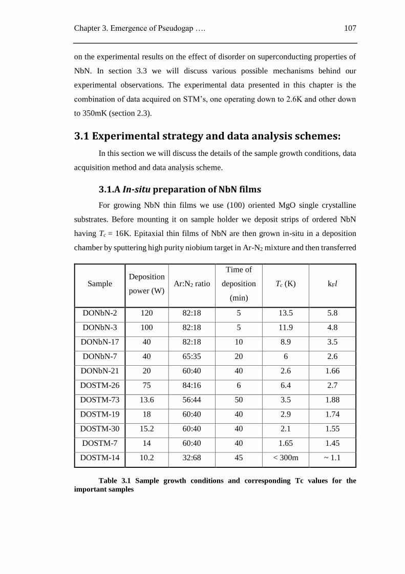
Chapter 3. Emergence of Pseudogap …. 107
on the experimental results on the effect of disorder on superconducting properties of
NbN. In section 3.3 we will discuss various possible mechanisms behind our
experimental observations. The experimental data presented in this chapter is the
combination of data acquired on STM’s, one operating down to 2.6K and other down
to 350mK (section 2.3).
3.1 Experimental strategy and data analysis schemes:
In this section we will discuss the details of the sample growth conditions, data
acquisition method and data analysis scheme.
3.1.A In-situ preparation of NbN films
For growing NbN thin films we use (100) oriented MgO single crystalline
substrates. Before mounting it on sample holder we deposit strips of ordered NbN
having Tc = 16K. Epitaxial thin films of NbN are then grown in-situ in a deposition
chamber by sputtering high purity niobium target in Ar-N2 mixture and then transferred
Sample Deposition
power (W) Ar:N2 ratio
Time of
deposition
(min)
Tc (K) kFl
DONbN-2 120 82:18 5 13.5 5.8
DONbN-3 100 82:18 5 11.9 4.8
DONbN-17 40 82:18 10 8.9 3.5
DONbN-7 40 65:35 20 6 2.6
DONbN-21 20 60:40 40 2.6 1.66
DOSTM-26 75 84:16 6 6.4 2.7
DOSTM-73 13.6 56:44 50 3.5 1.88
DOSTM-19 18 60:40 40 2.9 1.74
DOSTM-30 15.2 60:40 40 2.1 1.55
DOSTM-7 14 60:40 40 1.65 1.45
DOSTM-14 10.2 32:68 45 < 300m ~ 1.1
Table 3.1 Sample growth conditions and corresponding Tc values for the
important samples
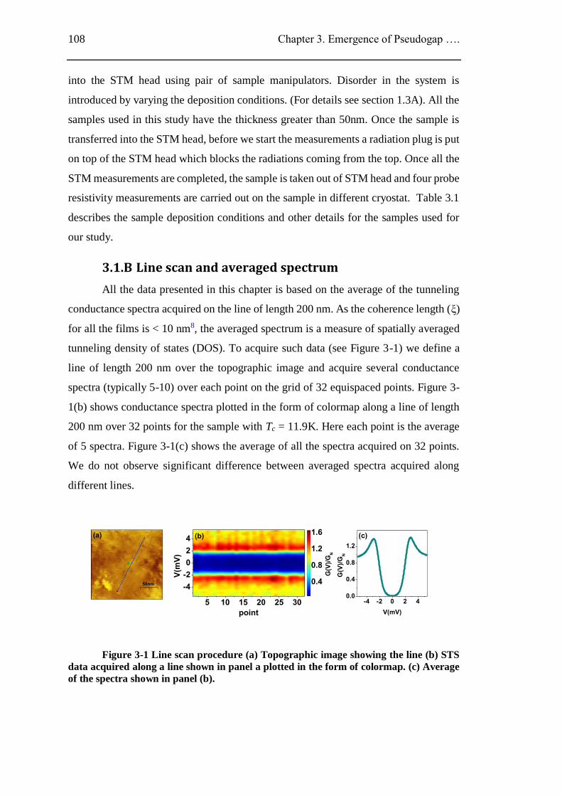
108 Chapter 3. Emergence of Pseudogap ….
into the STM head using pair of sample manipulators. Disorder in the system is
introduced by varying the deposition conditions. (For details see section 1.3A). All the
samples used in this study have the thickness greater than 50nm. Once the sample is
transferred into the STM head, before we start the measurements a radiation plug is put
on top of the STM head which blocks the radiations coming from the top. Once all the
STM measurements are completed, the sample is taken out of STM head and four probe
resistivity measurements are carried out on the sample in different cryostat. Table 3.1
describes the sample deposition conditions and other details for the samples used for
our study.
3.1.B Line scan and averaged spectrum
All the data presented in this chapter is based on the average of the tunneling
conductance spectra acquired on the line of length 200 nm. As the coherence length (ξ)
for all the films is < 10 nm8, the averaged spectrum is a measure of spatially averaged
tunneling density of states (DOS). To acquire such data (see Figure 3-1) we define a
line of length 200 nm over the topographic image and acquire several conductance
spectra (typically 5-10) over each point on the grid of 32 equispaced points. Figure 3-
1(b) shows conductance spectra plotted in the form of colormap along a line of length
200 nm over 32 points for the sample with Tc = 11.9K. Here each point is the average
of 5 spectra. Figure 3-1(c) shows the average of all the spectra acquired on 32 points.
We do not observe significant difference between averaged spectra acquired along
different lines.
-4 -2 0 2 40.0
0.4
0.8
1.2
(c)
G(V
)/G
N
G(V
)/G
N
V(mV)
(a)
5 10 15 20 25 30
-4
-2
0
2
4 (b)
V(m
V)
point
50nm 0.4
0.8
1.2
1.6
Figure 3-1 Line scan procedure (a) Topographic image showing the line (b) STS
data acquired along a line shown in panel a plotted in the form of colormap. (c) Average
of the spectra shown in panel (b).
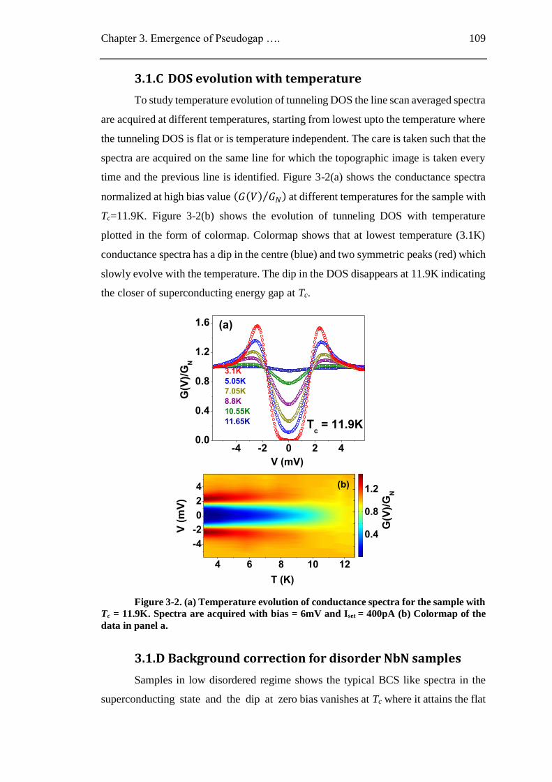
Chapter 3. Emergence of Pseudogap …. 109
3.1.C DOS evolution with temperature
To study temperature evolution of tunneling DOS the line scan averaged spectra
are acquired at different temperatures, starting from lowest upto the temperature where
the tunneling DOS is flat or is temperature independent. The care is taken such that the
spectra are acquired on the same line for which the topographic image is taken every
time and the previous line is identified. Figure 3-2(a) shows the conductance spectra
normalized at high bias value (𝐺(𝑉) 𝐺𝑁⁄ ) at different temperatures for the sample with
Tc=11.9K. Figure 3-2(b) shows the evolution of tunneling DOS with temperature
plotted in the form of colormap. Colormap shows that at lowest temperature (3.1K)
conductance spectra has a dip in the centre (blue) and two symmetric peaks (red) which
slowly evolve with the temperature. The dip in the DOS disappears at 11.9K indicating
the closer of superconducting energy gap at Tc.
4 6 8 10 12
-4
-2
0
2
4
-4 -2 0 2 40.0
0.4
0.8
1.2
1.6
Tc = 11.9K
G(V
)/G
N
V (mV)
3.1K
5.05K
7.05K
8.8K
10.55K
11.65K
(a)
(b)
G(V
)/G
N
V (
mV
)
T (K)
0.4
0.8
1.2
Figure 3-2. (a) Temperature evolution of conductance spectra for the sample with
Tc = 11.9K. Spectra are acquired with bias = 6mV and Iset = 400pA (b) Colormap of the
data in panel a.
3.1.D Background correction for disorder NbN samples
Samples in low disordered regime shows the typical BCS like spectra in the
superconducting state and the dip at zero bias vanishes at Tc where it attains the flat
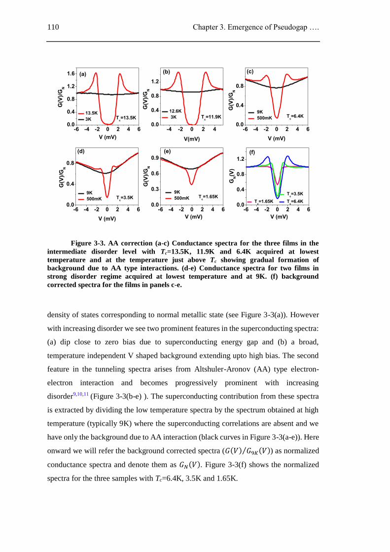
110 Chapter 3. Emergence of Pseudogap ….
-6 -4 -2 0 2 4 60.0
0.4
0.8
1.2
1.6
-4 -2 0 2 40.0
0.4
0.8
1.2
13.5K
3K
G(V
)/G
N
V (mV)
Tc=13.5K
(a)
Tc=11.9K
(b)
12.6K
3K
G(V
)/G
N
V(mV)
-6 -4 -2 0 2 4 60.0
0.4
0.8
(c)
9K
500mK
Tc=1.65KT
c=3.5K
G(V
)/G
N
V (mV)
Tc=6.4K
-6 -4 -2 0 2 4 60.0
0.4
0.8
(d)
9K
500mK
G(V
)/G
N
V (mV)
-6 -4 -2 0 2 4 60.0
0.3
0.6
0.9
(e)
9K
500mK
G
(V)/
GN
V (mV)
-6 -4 -2 0 2 4 60.0
0.4
0.8
1.2
(f)
Tc=3.5K
Tc=1.65K T
c=6.4K
GN(V
)
V (mV)
Figure 3-3. AA correction (a-c) Conductance spectra for the three films in the
intermediate disorder level with Tc=13.5K, 11.9K and 6.4K acquired at lowest
temperature and at the temperature just above Tc showing gradual formation of
background due to AA type interactions. (d-e) Conductance spectra for two films in
strong disorder regime acquired at lowest temperature and at 9K. (f) background
corrected spectra for the films in panels c-e.
density of states corresponding to normal metallic state (see Figure 3-3(a)). However
with increasing disorder we see two prominent features in the superconducting spectra:
(a) dip close to zero bias due to superconducting energy gap and (b) a broad,
temperature independent V shaped background extending upto high bias. The second
feature in the tunneling spectra arises from Altshuler-Aronov (AA) type electron-
electron interaction and becomes progressively prominent with increasing
disorder9,10,11 (Figure 3-3(b-e) ). The superconducting contribution from these spectra
is extracted by dividing the low temperature spectra by the spectrum obtained at high
temperature (typically 9K) where the superconducting correlations are absent and we
have only the background due to AA interaction (black curves in Figure 3-3(a-e)). Here
onward we will refer the background corrected spectra (𝐺(𝑉) 𝐺9𝐾(𝑉)⁄ ) as normalized
conductance spectra and denote them as 𝐺𝑁(𝑉). Figure 3-3(f) shows the normalized
spectra for the three samples with Tc=6.4K, 3.5K and 1.65K.
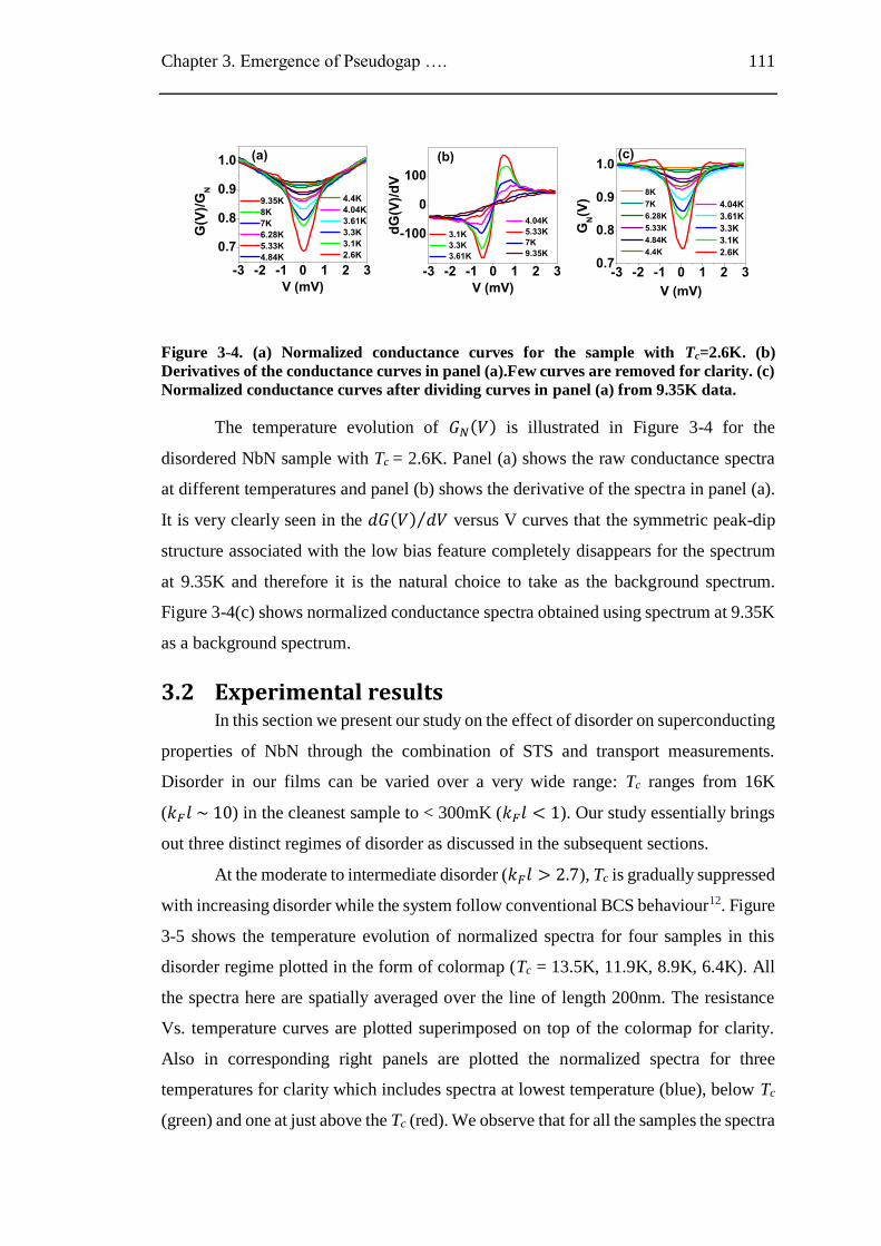
Chapter 3. Emergence of Pseudogap …. 111
-3 -2 -1 0 1 2 3
0.7
0.8
0.9
1.0
4.4K
4.04K
3.61K
3.3K
3.1K
2.6K
G(V
)/G
N
V (mV)
(a)
-3 -2 -1 0 1 2 30.7
0.8
0.9
1.0(c)
4.04K
3.61K
3.3K
3.1K
2.6K
8K
7K
6.28K
5.33K
4.84K
4.4K
GN(V
)
V (mV)
-3 -2 -1 0 1 2 3
-100
0
100
(b)
3.1K
3.3K
3.61K
4.04K
5.33K
7K
9.35K
9.35K
8K
7K
6.28K
5.33K
4.84K
dG
(V)/
dV
V (mV)
Figure 3-4. (a) Normalized conductance curves for the sample with Tc=2.6K. (b)
Derivatives of the conductance curves in panel (a).Few curves are removed for clarity. (c)
Normalized conductance curves after dividing curves in panel (a) from 9.35K data.
The temperature evolution of 𝐺𝑁(𝑉) is illustrated in Figure 3-4 for the
disordered NbN sample with Tc = 2.6K. Panel (a) shows the raw conductance spectra
at different temperatures and panel (b) shows the derivative of the spectra in panel (a).
It is very clearly seen in the 𝑑𝐺(𝑉) 𝑑𝑉⁄ versus V curves that the symmetric peak-dip
structure associated with the low bias feature completely disappears for the spectrum
at 9.35K and therefore it is the natural choice to take as the background spectrum.
Figure 3-4(c) shows normalized conductance spectra obtained using spectrum at 9.35K
as a background spectrum.
3.2 Experimental results In this section we present our study on the effect of disorder on superconducting
properties of NbN through the combination of STS and transport measurements.
Disorder in our films can be varied over a very wide range: Tc ranges from 16K
(𝑘𝐹𝑙 ~ 10) in the cleanest sample to < 300mK (𝑘𝐹𝑙 < 1). Our study essentially brings
out three distinct regimes of disorder as discussed in the subsequent sections.
At the moderate to intermediate disorder (𝑘𝐹𝑙 > 2.7), Tc is gradually suppressed
with increasing disorder while the system follow conventional BCS behaviour12. Figure
3-5 shows the temperature evolution of normalized spectra for four samples in this
disorder regime plotted in the form of colormap (Tc = 13.5K, 11.9K, 8.9K, 6.4K). All
the spectra here are spatially averaged over the line of length 200nm. The resistance
Vs. temperature curves are plotted superimposed on top of the colormap for clarity.
Also in corresponding right panels are plotted the normalized spectra for three
temperatures for clarity which includes spectra at lowest temperature (blue), below Tc
(green) and one at just above the Tc (red). We observe that for all the samples the spectra
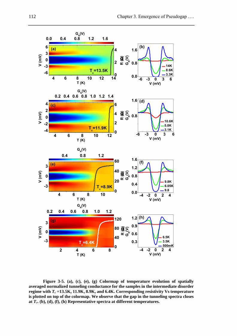
112 Chapter 3. Emergence of Pseudogap ….
4 6 8 10 12 14
-6
-3
0
3
6 (a)
Tc=11.9K
Tc=13.5K
V (
mV
)
T (K)
0
2
4
R (
) R
(
) R
(
) R
(
)
0.0 0.4 0.8 1.2 1.6
GN(V)
GN(V)
GN(V)
GN(V)
-6 -3 0 3 60.0
0.8
1.6(b)
14K
8.6K
3.3K
GN(V
)
V (mV)
4 6 8 10 12
-4
-2
0
2
4 (c)
V (
mV
)
T (K)
0
2
4
6
0.2 0.4 0.6 0.8 1.0 1.2 1.4
-6 -3 0 3 6
0.8
1.6 (d)
10.6K
5.8K
3.1K
GN(V
)
V (mV)
4 6 8 10
-3
0
3(e)
Tc=8.9K
V (
mV
)
T (K)
0
20
40
60
0.4 0.8 1.2
-4 -2 0 2 40.0
0.4
0.8
1.2
1.6(f)
9.8K
6.05K
9.8
GN(V
)
V (mV)
2 4 6 8
-3
0
3
Tc=6.4K
V (
mV
)
T (K)
0
40
80
120
0.2 0.4 0.6 0.8 1.0 1.2
(g)
-4 -2 0 2 4
0.3
0.6
0.9
1.2 (h)
6.5K
3.5K
500mK
GN(V
)
V (mV)
Figure 3-5. (a), (c), (e), (g) Colormap of temperature evolution of spatially
averaged normalized tunneling conductance for the samples in the intermediate disorder
regime with Tc =13.5K, 11.9K, 8.9K, and 6.4K. Corresponding resistivity Vs temperature
is plotted on top of the colormap. We observe that the gap in the tunneling spectra closes
at Tc. (b), (d), (f), (h) Representative spectra at different temperatures.
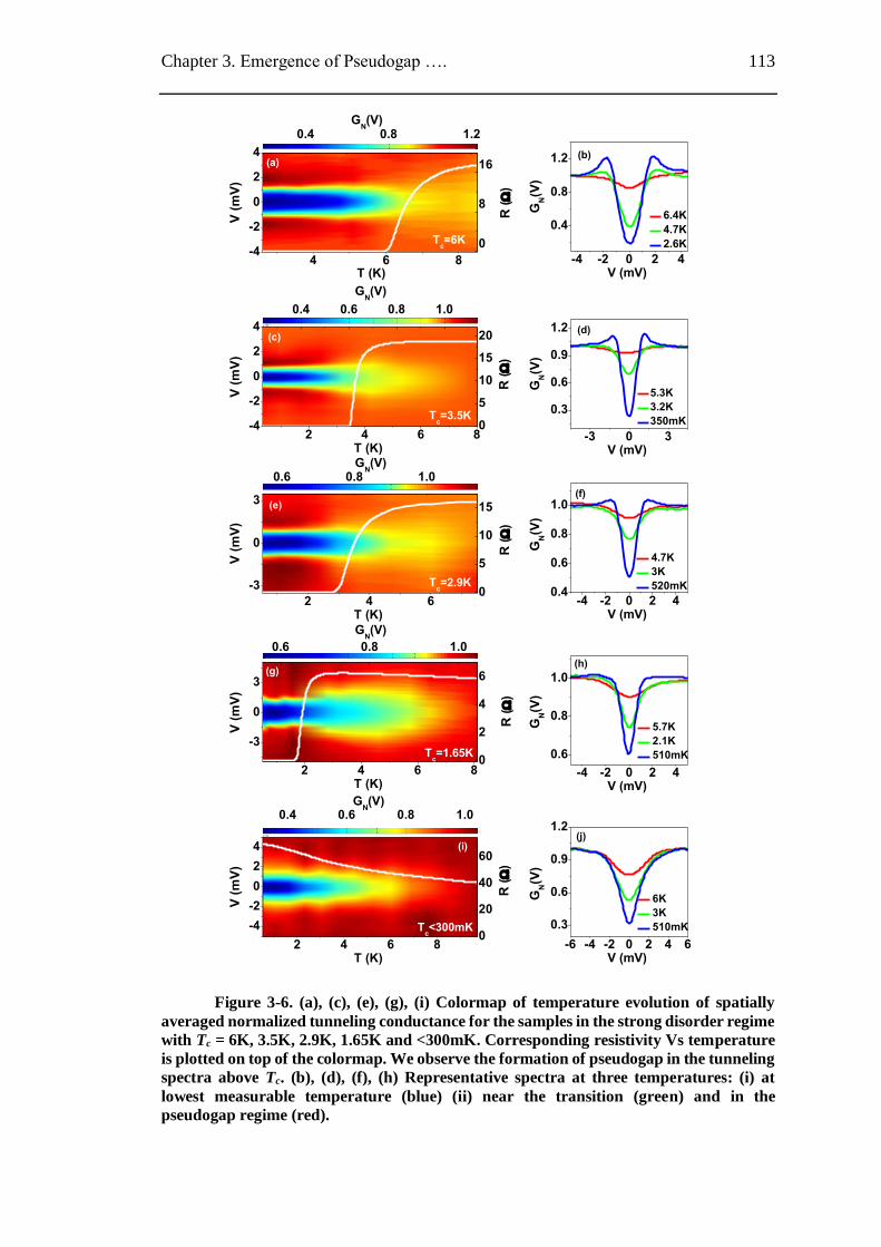
Chapter 3. Emergence of Pseudogap …. 113
4 6 8-4
-2
0
2
4
V (
mV
)
T (K)
Tc=6K
(a)
0
8
16
Tc=3.5K
R (
) R
(
) R
(
) R
(
) R
(
)
0.4 0.8 1.2
GN(V)
GN(V)
GN(V)
GN(V)
GN(V)
-4 -2 0 2 4
0.4
0.8
1.2 (b)
6.4K
4.7K
2.6K
GN(V
)
V (mV)
2 4 6 8-4
-2
0
2
4(c)
V (
mV
)
T (K)
0
5
10
15
20
0.4 0.6 0.8 1.0
-3 0 3
0.3
0.6
0.9
1.2 (d)
5.3K
3.2K
350mK
GN(V
)
V (mV)
2 4 6
-3
0
3 (e)
Tc=2.9K
V (
mV
)
T (K)
0
5
10
15
0.6 0.8 1.0
-4 -2 0 2 40.4
0.6
0.8
1.0(f)
4.7K
3K
520mK
GN(V
)
V (mV)
2 4 6 8
-3
0
3(g)
Tc<300mK
Tc=1.65K
Tc=1.65K
V (
mV
)
T (K)
0
2
4
6
0.6 0.8 1.0
-4 -2 0 2 4
0.6
0.8
1.0(h)
5.7K
2.1K
510mK
GN(V
)
V (mV)
2 4 6 8
-4
-2
0
2
4(j)
(i)
V (
mV
)
T (K)
0
20
40
60
0.4 0.6 0.8 1.0
-6 -4 -2 0 2 4 6
0.3
0.6
0.9
1.2
6K
3K
510mK
GN(V
)
V (mV)
Figure 3-6. (a), (c), (e), (g), (i) Colormap of temperature evolution of spatially
averaged normalized tunneling conductance for the samples in the strong disorder regime
with Tc = 6K, 3.5K, 2.9K, 1.65K and <300mK. Corresponding resistivity Vs temperature
is plotted on top of the colormap. We observe the formation of pseudogap in the tunneling
spectra above Tc. (b), (d), (f), (h) Representative spectra at three temperatures: (i) at
lowest measurable temperature (blue) (ii) near the transition (green) and in the
pseudogap regime (red).
114 Chapter 3. Emergence of Pseudogap ….
at low temperature show a prominent gap and two symmetric coherence peaks. The
superconducting gap vanishes exactly at Tc as expected from BCS theory and a flat
metallic DOS is restored above Tc.
With further increase in disorder (2.7 > 𝑘𝐹𝑙 > 1) Tc continue to decrease
monotonically while we observe the emergence of pseudogap state where the finite gap
above Tc is revealed though STS measurements. The temperature at which pseudogap
vanishes is denoted by T*. For practical purposes we define T* as the temperature at
which the zero bias conductance (ZBC) value in the normalized conductance spectra
become 95% of the value at high bias. Figure 3-6 shows colormap of temperature
evolution of normalized conductance spectra for five samples with Tc = 6K, 3.5K, 2.9K,
1.65K and < 300mK. Three spectra are shown on the corresponding right side panels
for clarity which include the spectra at lowest temperature (blue), near Tc (green) and
one in the pseudogap region (red). Figure 3-6 reveals that with increasing disorder T*/Tc
increases. For sample with Tc = 1.65, T* > 4Tc while for the sample with Tc < 300mK,
T* >> Tc. Interesting thing to notice in all our strongly disordered samples is that T*
has the value ~ 6 -7K irrespective of the value of Tc. The pseudogap state has also been
observed in other strongly disordered conventional s-wave superconductors like
TiN13and InO,14 consistent with our results.
All the above results are summarized in the Figure 3-7 in the form of phase
diagram where we plot evolution of Tc and T* as a function of 𝑘𝐹𝑙. The phase diagram
brings out three distinct regimes: the intermediate regime (regime I) where the
superconducting state is characterized by a single energy scale Tc, strong disorder
regime (regime II) which is characterized by the emergence of the pseudogap state and
a nonsuperconducting regime (regime III) where the samples remain
nonsuperconducting down to 300mK.
3.3 Discussion
Before we understand the effect of disorder to decrease Tc and emergence of
pseudogap state we will discuss the possible mechanisms responsible for the
destruction of superconductivity. The superconducting state is characterized by a
complex order parameter,
Ψ = |Δ|𝑒𝑖𝜑 (3.1)
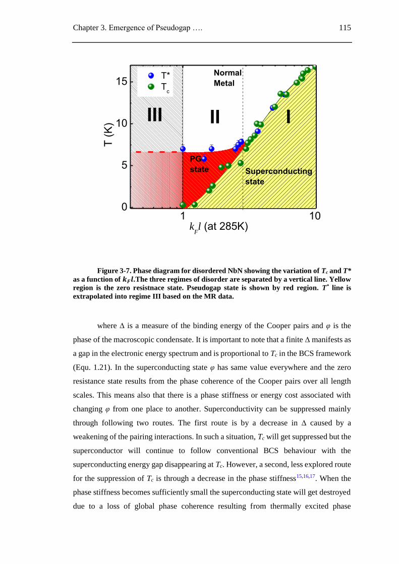
Chapter 3. Emergence of Pseudogap …. 115
1 100
5
10
15T*
Tc
PG
state Superconducting
state
III II
T (
K)
kFl (at 285K)
I
Normal
Metal
Figure 3-7. Phase diagram for disordered NbN showing the variation of Tc and T*
as a function of 𝒌𝑭𝒍.The three regimes of disorder are separated by a vertical line. Yellow
region is the zero resistnace state. Pseudogap state is shown by red region. T* line is
extrapolated into regime III based on the MR data.
where ∆ is a measure of the binding energy of the Cooper pairs and φ is the
phase of the macroscopic condensate. It is important to note that a finite ∆ manifests as
a gap in the electronic energy spectrum and is proportional to Tc in the BCS framework
(Equ. 1.21). In the superconducting state φ has same value everywhere and the zero
resistance state results from the phase coherence of the Cooper pairs over all length
scales. This means also that there is a phase stiffness or energy cost associated with
changing φ from one place to another. Superconductivity can be suppressed mainly
through following two routes. The first route is by a decrease in ∆ caused by a
weakening of the pairing interactions. In such a situation, Tc will get suppressed but the
superconductor will continue to follow conventional BCS behaviour with the
superconducting energy gap disappearing at Tc. However, a second, less explored route
for the suppression of Tc is through a decrease in the phase stiffness15,16,17. When the
phase stiffness becomes sufficiently small the superconducting state will get destroyed
due to a loss of global phase coherence resulting from thermally excited phase
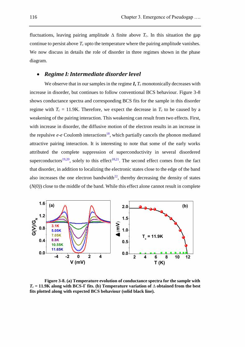
116 Chapter 3. Emergence of Pseudogap ….
fluctuations, leaving pairing amplitude ∆ finite above Tc. In this situation the gap
continue to persist above Tc upto the temperature where the pairing amplitude vanishes.
We now discuss in details the role of disorder in three regimes shown in the phase
diagram.
Regime I: Intermediate disorder level
We observe that in our samples in the regime I, Tc monotonically decreases with
increase in disorder, but continues to follow conventional BCS behaviour. Figure 3-8
shows conductance spectra and corresponding BCS fits for the sample in this disorder
regime with Tc = 11.9K. Therefore, we expect the decrease in Tc to be caused by a
weakening of the pairing interaction. This weakening can result from two effects. First,
with increase in disorder, the diffusive motion of the electron results in an increase in
the repulsive e-e Coulomb interactions18, which partially cancels the phonon mediated
attractive pairing interaction. It is interesting to note that some of the early works
attributed the complete suppression of superconductivity in several disordered
superconductors19,20, solely to this effect18,21. The second effect comes from the fact
that disorder, in addition to localizing the electronic states close to the edge of the band
also increases the one electron bandwidth22, thereby decreasing the density of states
(N(0)) close to the middle of the band. While this effect alone cannot result in complete
2 4 6 8 10 120.0
0.5
1.0
1.5
2.0
-4 -2 0 2 40.0
0.4
0.8
1.2
1.6
G(V
)/G
N
V (mV)
3.1K
5.05K
7.05K
8.8K
10.55K
11.65K
Tc = 11.9K
(a) (b)
m
V
T (K)
Figure 3-8. (a) Temperature evolution of conductance spectra for the sample with
Tc = 11.9K along with BCS-Γ fits. (b) Temperature variation of ∆ obtained from the best
fits plotted along with expected BCS behaviour (solid black line).
Chapter 3. Emergence of Pseudogap …. 117
suppression of superconductivity, it can have a noticeable effect in the intermediate
disordered regime23. Both these effects are captured at a qualitative level using the
modified BCS relation24,
𝑇𝑐 = 1.13Θ𝐷𝑒𝑥𝑝 (−1
𝑁(0)𝑉 − 𝜇∗) (3.2)
where Θ𝐷 is a temperature scale of the order of Debye temperature, V is the
attractive electron-phonon potential and 𝜇∗ is the Coulomb pseudopotential which
accounts for the disorder enhanced e-e interactions. The available theoretical model on
the dependence of the 𝜇∗ on disorder in a 3-D superconductor is currently not developed
enough to attempt a quantitative fit of our data. However the combination of the two
effects mentioned above qualitatively explains the suppression of Tc in the intermediate
disorder level, where the superconducting energy gap in the tunneling DOS vanishes
exactly at Tc.
Regime II: Strong disorder level
Strong disorder regime is characterized by two temperature scales, namely, Tc,
which corresponds to the temperature at which the resistance appears and T*, the
pseudogap temperature where the gap in the local tunneling spectra disappears. Tc
continues to decrease monotonically with increasing disorder, whereas T* remains
almost constant down to 𝑘𝐹𝑙 ~ 1, where the superconducting ground state is completely
destroyed. It would be natural to ascribe these two temperature scales to the phase
stiffness of the superfluid (J) and the strength of the pairing interaction () respectively.
J can be estimated using the relation15,16,
𝐽 =ℏ𝑎𝑛𝑠4𝑚∗
(3.3)
where a is the length scale over which the phase fluctuates and m* is the
effective mass of the electron. A rough estimate of J is obtained from 𝑛𝑠 derived from
the low temperature penetration depth25 (𝜆(𝑇 → 0)) and setting a in the
equation ,
𝑛𝑠 =𝑚∗
𝜇0𝑒2𝜆2 (3.4)
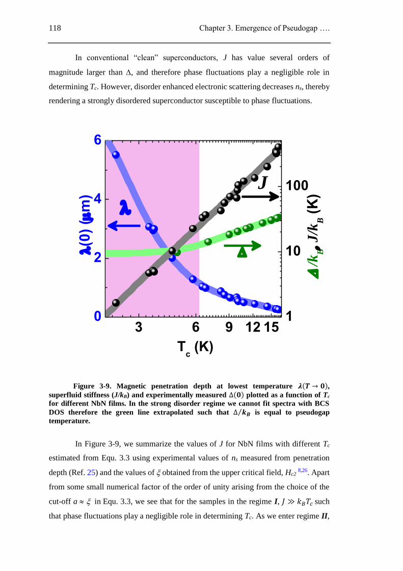
118 Chapter 3. Emergence of Pseudogap ….
In conventional “clean” superconductors, J has value several orders of
magnitude larger than , and therefore phase fluctuations play a negligible role in
determining Tc. However, disorder enhanced electronic scattering decreases ns, thereby
rendering a strongly disordered superconductor susceptible to phase fluctuations.
3 6 9 12 150
2
4
6
(0
) (
m)
Tc (K)
J
1
10
100
/
kBJ
/kB (
K)
Figure 3-9. Magnetic penetration depth at lowest temperature 𝝀(𝑻 → 𝟎), superfluid stiffness (J/kB) and experimentally measured ∆(𝟎) plotted as a function of Tc
for different NbN films. In the strong disorder regime we cannot fit spectra with BCS
DOS therefore the green line extrapolated such that ∆ 𝒌𝑩⁄ is equal to pseudogap
temperature.
In Figure 3-9, we summarize the values of J for NbN films with different Tc
estimated from Equ. 3.3 using experimental values of ns measured from penetration
depth (Ref. 25) and the values of obtained from the upper critical field, Hc2 8,26. Apart
from some small numerical factor of the order of unity arising from the choice of the
cut-off a inEqu. 3.3, we see that for the samples in the regime I, 𝐽 ≫ 𝑘𝐵𝑇𝑐 such
that phase fluctuations play a negligible role in determining Tc. As we enter regime II,
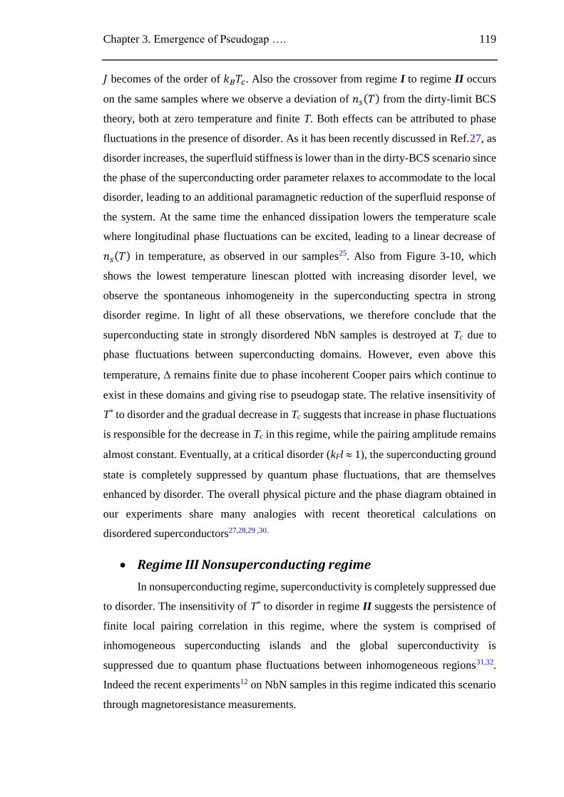
Chapter 3. Emergence of Pseudogap …. 119
𝐽 becomes of the order of 𝑘𝐵𝑇𝑐. Also the crossover from regime I to regime II occurs
on the same samples where we observe a deviation of 𝑛𝑠(𝑇) from the dirty-limit BCS
theory, both at zero temperature and finite T. Both effects can be attributed to phase
fluctuations in the presence of disorder. As it has been recently discussed in Ref.27, as
disorder increases, the superfluid stiffness is lower than in the dirty-BCS scenario since
the phase of the superconducting order parameter relaxes to accommodate to the local
disorder, leading to an additional paramagnetic reduction of the superfluid response of
the system. At the same time the enhanced dissipation lowers the temperature scale
where longitudinal phase fluctuations can be excited, leading to a linear decrease of
𝑛𝑠(𝑇) in temperature, as observed in our samples25. Also from Figure 3-10, which
shows the lowest temperature linescan plotted with increasing disorder level, we
observe the spontaneous inhomogeneity in the superconducting spectra in strong
disorder regime. In light of all these observations, we therefore conclude that the
superconducting state in strongly disordered NbN samples is destroyed at Tc due to
phase fluctuations between superconducting domains. However, even above this
temperature, remains finite due to phase incoherent Cooper pairs which continue to
exist in these domains and giving rise to pseudogap state. The relative insensitivity of
T* to disorder and the gradual decrease in Tc suggests that increase in phase fluctuations
is responsible for the decrease in Tc in this regime, while the pairing amplitude remains
almost constant. Eventually, at a critical disorder (kFl 1), the superconducting ground
state is completely suppressed by quantum phase fluctuations, that are themselves
enhanced by disorder. The overall physical picture and the phase diagram obtained in
our experiments share many analogies with recent theoretical calculations on
disordered superconductors27,28,29 ,30.
Regime III Nonsuperconducting regime
In nonsuperconducting regime, superconductivity is completely suppressed due
to disorder. The insensitivity of T* to disorder in regime II suggests the persistence of
finite local pairing correlation in this regime, where the system is comprised of
inhomogeneous superconducting islands and the global superconductivity is
suppressed due to quantum phase fluctuations between inhomogeneous regions31,32.
Indeed the recent experiments12 on NbN samples in this regime indicated this scenario
through magnetoresistance measurements.
120 Chapter 3. Emergence of Pseudogap ….
10 20 30
-4
-2
0
2
4
Tc=13.5K
(a)
V(m
V)
Point
0.4
0.8
1.2
GN(V
)
GN(V
)
GN(V
)
GN(V
)
GN(V
)
GN(V
)
GN(V
)
GN(V
)
10 20 30
-4
-2
0
2
4
Tc=11.9K
(b)
V(m
V)
Point
0.4
0.8
1.2
1.6
10 20 30
-4
-2
0
2
4
Tc=6.4K
(c)
V(m
V)
Point
0.5
1.0
1.5
10 20 30
-4
-2
0
2
4
Tc=6K
(d)
V(m
V)
Point
0.4
0.8
1.2
10 20 30
-4
-2
0
2
4
Tc=3.5K
(e)
V(m
V)
Point
0.5
1.0
1.5
10 20 30
-4
-2
0
2
4
Tc=2.9K
(f)
V(m
V)
Point
0.4
0.8
1.2
10 20 30
-4
-2
0
2
4
Tc=2.1K
(g)
V(m
V)
Point
0.6
0.8
1.0
1.2
10 20 30
-4
-2
0
2
4
Tc=1.65K
(h)
V(m
V)
Point
0.6
0.8
1.0
Figure 3-10. Line scans acquired at lowest temperature for 8 films with different
levels of disorder. We can see that for the samples with Tc ≤ 6K superconductivity
becomes inhomogeneous supporting phase fluctuation scenario.
3.4 Summary
We have shown that with increasing disorder a 3D conventional
superconductor, NbN, evolves from a BCS superconductor in a moderately clean limit
to the situation where the superconductivity is completely destroyed through phase
fluctuations. We constructed a temperature-disorder (T-𝑘𝐹𝑙) phase diagram
Chapter 3. Emergence of Pseudogap …. 121
summarizing various temperature scales based on the transport and STS measurements.
We identify three distinct regimes of disorder on the phase diagram: (i) the intermediate
disorder regime where Tc monotonically decreases due to weakening of pairing
interaction, (ii) strong disorder regime where the decrease in Tc is governed by phase
fluctuations and (iii) nonsuperconducting. It would be interesting to explore the analogy
with underdoped high-Tc cuprates, which share many similarities with strongly
disordered s-wave superconductors.
3.5 References
1 Tinkham, M Introduction to Superconductivity (Dover Publications Inc., Mineola,
New York, 2004).
2 T. Kondo, R. Khasanov, T. Takeuchi, J. Schmalian and A. Kaminski, Competition
between the pseudogap and superconductivity in the high-Tc copper oxides, Nature
457, 296-300 (2009)
3 M. Hashimoto et al, Particle–hole symmetry breaking in the pseudogap state of
Bi2201, Nature Physics 6, 414–418 (2010).
4 Ch. Renner, B. Revaz, J.-Y. Genoud, K. Kadowaki, and Ø. Fischer, Pseudogap
Precursor of the Superconducting Gap in Under- and Overdoped Bi2Sr2CaCu2O8+δ,
Phys. Rev. Lett. 80, 149–152 (1998)
5 M. Kugler, Ø. Fischer, Ch. Renner, S. Ono and Yoichi Ando, Scanning Tunneling
Spectroscopy of Bi2Sr2CuO6+δ: New Evidence for the Common Origin of the
Pseudogap and Superconductivity, Phys. Rev. Lett. 86, 4911–4914 (2001)
6 Y. Kohsaka et al, How Cooper pairs vanish approaching the Mott insulator in
Bi2Sr2CaCu2O8+δ, Nature 454, 1072-1078 (2008).
7 A. Kamlapure, M. Mondal, M. Chand, A. Mishra, J. Jesudasan, V. Bagwe, L.
Benfatto, V. Tripathi, and P. Raychaudhuri, Measurement of magnetic penetration
122 Chapter 3. Emergence of Pseudogap ….
depth and superconducting energy gap in very thin epitaxial NbN films, Appl. Phys.
Lett. 96, 072509 (2010).
8 Madhavi Chand, Ph.D. Thesis, Tata Institute of Fundamental Research, 2013
http://www.tifr.res.in/~superconductivity/pdfs/madhavi.pdf
9 B. L. Altshuler and A. G. Aronov Zero Bias Anomaly in Tunnel Resistance and
Electron-electron Interaction. Solid State Commun. 36, 115-117 (1979).
10 B. L. Altshuler and A. G. Aronov In: Electron-Electron Interactions in Disordered
Systems, edited by Pollak, M.; Efros, A. L. Ed. North-Holland, Amsterdam, 1984,
Chapter 1.
11 B. L. Altshuler, A. G. Aronov and P. A. Lee, Interaction Effects in Disordered
Fermi Systems in Two Dimensions, Phys. Rev. Lett. 44, 1288–1291 (1980)
12 M. Chand, G. Saraswat, A. Kamlapure, M. Mondal, S. Kumar, J. Jesudasan, V.
Bagwe, L. Benfatto, V. Tripathi, and P. Raychaudhuri, Phase diagram of a strongly
disordered s-wave superconductor, NbN, close to the metal-insulator transition. Phys.
Rev. B 85, 014508 (2012).
13 B. Sacépé, C. Chapelier, T. I. Baturina, V. M.Vinokur, M. R. Baklanov and M.
Sanquer, Pseudogap in a thin film of a conventional superconductor, Nat. Commun. 1
140 (2010)
14 B. Sacépé, T. Dubouchet, C. Chapelier, M. Sanquer, M. Ovadia, D. Shahar, M.
Feigel’man and L. Ioffe, Localization of preformed Cooper pairs in disordered
superconductors, Nat. Phys. 7 239 (2011)
15 V. J. Emery and S. A. Kivelson, Importance of phase fluctuations in
superconductors with small superfluid density, Nature (London) 374, 434 (1995)
16 V. J. Emery and S. A. Kivelson, Superconductivity in Bad Metals, Phys. Rev. Lett.
74, 3253 (1995).
17 T. V. Ramakrishnan, Superconductivity in disordered thin films, Phys. Scr., T 27,
24 (1989). 18 P. W. Anderson, K. A. Muttalib and T. V. Ramakrishnan, Theory of the "universal"
degradation of Tc in high-temperature superconductors, Phys. Rev. B 28, 117 (1983).
19 T. Furubayashi, N. Nishida, M. Yamaguchi, K. Morigaki, H. Ishimoto,
Superconducting properties of amorphous Si1−xAux near metal-insulator transition,
Solid State Commun. 55, 513 (1985).
Chapter 3. Emergence of Pseudogap …. 123
20 G. Hertel, D. J. Bishop, E. G. Spencer, J. M. Rowell, and R. C. Dynes, Tunneling
and Transport Measurements at the Metal-Insulator Transition of Amorphous Nb: Si,
Phys. Rev. Lett. 50, 743 (1983).
21 A. M. Finkelstein, Suppression of superconductivity in homogeneously disordered
systems, Physica B 197, 636-648 (1994).
22 J. M. Ziman, Models of Disorder, (Cambridge University Press, 1979).
23 A. Ghosal, M. Randeria, and N. Trivedi, Inhomogeneous pairing in highly
disordered s-wave superconductors, Phys. Rev. B 65, 014501 (2001).
24 W. L. McMillan, Transition Temperature of Strong-Coupled Superconductors,
Phys. Rev. 167, 331 (1968).
25 M. Mondal, A. Kamlapure, M. Chand, G. Saraswat, S. Kumar, J. Jesudasan, L.
Benfatto, V. Tripathi and P. Raychaudhuri, Phase fluctuations in a strongly
disordered s-wave NbN superconductor close to the Metal-Insulator transition, Phys.
Rev. Lett. 106, 047001 (2011).
26 M. Mondal, M. Chand, A. Kamlapure, J. Jesudasan, V. C. Bagwe, S. Kumar, G.
Saraswat, V. Tripathi and P. Raychaudhuri, Phase Diagram and Upper Critical Field
of Homogeneously Disordered Epitaxial 3-Dimensional NbN Films, J. Supercond.
Nov. Magn. 24, 341 (2011).
27 G. Seibold, L. Benfatto, C. Castellani and J. Lorenzana, Superfluid Density and
Phase Relaxation in Superconductors with Strong Disorder, Phys. Rev. Lett. 108,
207004 (2012)
28 A. Ghosal, M. Randeria, and N. Trivedi, Inhomogeneous pairing in highly
disordered s-wave superconductors, Phys. Rev. B 65, 014501 (2001).
29 A. Ghosal, M. Randeria, and N. Trivedi, Role of Spatial Amplitude Fluctuations in
Highly Disordered s-Wave Superconductors, Phys. Rev. Lett. 81, 3940–3943 (1998)
30 X. T. Wu and R. Ikeda, Pseudogap phase in strongly disordered conventional
superconductors, Phys. Rev. B 83, 104517 (2011).
31 Y. Dubi, Y. Meir and Y. Avishai, Theory of the magnetoresistance of disordered
superconducting films, Phys. Rev. B 73, 054509 (2006).

124 Chapter 3. Emergence of Pseudogap ….
32 M. Müller, Magnetoresistance and localization in bosonic insulators, EPL 102
67008 (2013)
Chapter 4
Emergence of inhomogeneity in the superconducting state of strongly disordered s-wave superconductor, NbN
4.1 Introduction
In recent times numerous theories and numerical simulations have been carried
out in order to understand real space evolution of superconductivity in presence of
strong disorder. The starting Hamiltonian for the superconductor is normally the
attractive Hubbard model with random on-site energy1,2,3. Although these simulations
ignore the Coulomb interactions and are done on relatively small lattice the end results
are instructive. These simulations indicate that in the presence of strong disorder the
superconducting order parameter becomes inhomogeneous, spontaneously segregating
into superconducting domains, dispersed in an insulating matrix. Consequently the
energy gap Δ is not strongly affected but the energy cost of spatially twisting the phase
of the condensate, the superfluid stiffness J, decreases rapidly with increasing disorder
making the system more susceptible to phase fluctuations. Thus in presence of strong
disorder and below the critical disorder system consists of superconducting islands and
the phases are Josephson coupled through insulating regions in the superconducting
state. These superconducting islands lose phase coherence above Tc but persists upto
much higher temperatures.
While the formation of an inhomogeneous superconducting state has been
invoked to explain a variety of phenomena close to the critical disorder for the
destruction of the superconducting state e.g. magnetic field tuned superconductor-
insulator transition4,5, finite superfluid stiffness6 above Tc and Little-Parks oscillations
in a disorder driven insulating film7,8, a direct experimental proof of emergent
126 Chapter 4. Emergence of inhomogeneity …
inhomogeneity in a system where the structural disorder is indeed homogeneously
distributed over typical length scale of superconducting domains is currently lacking.
In this chapter we use a low temperature scanning tunneling microscope (LT-
STM) to explore the inhomogeneity formed in the superconducting ground state in
homogeneously disordered NbN. In combination we also use high resolution scanning
transmission electron microscope (HRSTEM) to study the structural disorder at the
atomic length scale. Indeed we see the emergence of inhomogeneity in the local order
parameter in the form of domains of size over tens of nanometer while the structural
disorder is distributed uniformly over atomic scale. We also observe the striking
universality in the order parameter distribution when we rescale the order parameter by
taking logarithm and normalizing to its variance.
The plan of the chapter is as follows, in section 4.2 we first explore the structural
disorder in NbN at the atomic scale probed through HRSTEM. In next few sections
we discuss the general trend in the superconducting spectra with increasing disorder
through scanning tunneling spectroscopy (STS) measurements and define the order
parameter for the disordered superconducting state. In section 4.6 we discuss the
emergent inhomogeneity and its spatial correlation. In section 4.7 we explore the
universality in the order parameter distribution. We report the temperature evolution of
the inhomogeneous superconducting state across Tc in section 4.8. Finally we discuss
the implication of our results in concluding section.
4.2 Investigation of structural disorder in NbN at the
atomic scale.
To characterise the disorder at the atomic scale HRSTEM measurements were
performed on two films: one with low disorder having Tc ~ 16K and other is strongly
disordered sample having Tc ~ 2.5K (𝑘𝐹𝑙 ~ 1.7). To make the interfaces 'edge on', i.e,
perpendicular to the incoming electron beam, both the samples were tilted along <110>
in this present study. The structure of NbN projected along <110> is shown in the inset
of Figure 4-1(a) which reveals that atomic columns contain either Nb or, N i.e, atomic
columns with mixed atoms are not present while viewing through this direction. High
resolution Z-contrast images of MgO/NbN thin film interfaces of both samples (Figure
4-1(a) and (g)) shows that the films grow epitaxially on MgO (100) substrate. At low
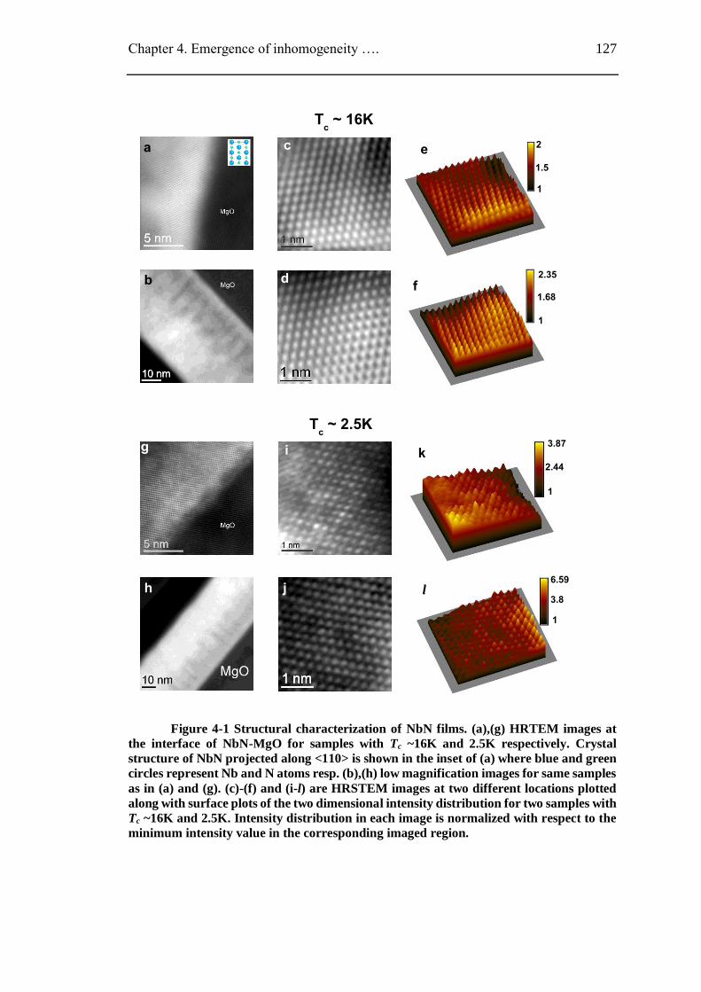
Chapter 4. Emergence of inhomogeneity …. 127
Tc ~ 2.5K
lj
1
3.8
6.59
1
2.44
3.87
h
kig
f
e
d
c
b
1
1.68
2.35
1.5
2
1
a
Tc ~ 16K
Figure 4-1 Structural characterization of NbN films. (a),(g) HRTEM images at
the interface of NbN-MgO for samples with Tc ~16K and 2.5K respectively. Crystal
structure of NbN projected along <110> is shown in the inset of (a) where blue and green
circles represent Nb and N atoms resp. (b),(h) low magnification images for same samples
as in (a) and (g). (c)-(f) and (i-l) are HRSTEM images at two different locations plotted
along with surface plots of the two dimensional intensity distribution for two samples with
Tc ~16K and 2.5K. Intensity distribution in each image is normalized with respect to the
minimum intensity value in the corresponding imaged region.
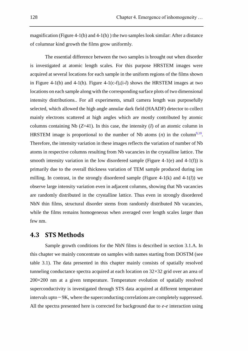
128 Chapter 4. Emergence of inhomogeneity …
magnification (Figure 4-1(b) and 4-1(h) ) the two samples look similar: After a distance
of columnar kind growth the films grow uniformly.
The essential difference between the two samples is brought out when disorder
is investigated at atomic length scales. For this purpose HRSTEM images were
acquired at several locations for each sample in the uniform regions of the films shown
in Figure 4-1(b) and 4-1(h). Figure 4-1(c-f),(i-l) shows the HRSTEM images at two
locations on each sample along with the corresponding surface plots of two dimensional
intensity distributions.. For all experiments, small camera length was purposefully
selected, which allowed the high angle annular dark field (HAADF) detector to collect
mainly electrons scattered at high angles which are mostly contributed by atomic
columns containing Nb (Z=41). In this case, the intensity (I) of an atomic column in
HRSTEM image is proportional to the number of Nb atoms (n) in the column9,10.
Therefore, the intensity variation in these images reflects the variation of number of Nb
atoms in respective columns resulting from Nb vacancies in the crystalline lattice. The
smooth intensity variation in the low disordered sample (Figure 4-1(e) and 4-1(f)) is
primarily due to the overall thickness variation of TEM sample produced during ion
milling. In contrast, in the strongly disordered sample (Figure 4-1(k) and 4-1(l)) we
observe large intensity variation even in adjacent columns, showing that Nb vacancies
are randomly distributed in the crystalline lattice. Thus even in strongly disordered
NbN thin films, structural disorder stems from randomly distributed Nb vacancies,
while the films remains homogeneous when averaged over length scales larger than
few nm.
4.3 STS Methods
Sample growth conditions for the NbN films is described in section 3.1.A. In
this chapter we mainly concentrate on samples with names starting from DOSTM (see
table 3.1). The data presented in this chapter mainly consists of spatially resolved
tunneling conductance spectra acquired at each location on 32×32 grid over an area of
200×200 nm at a given temperature. Temperature evolution of spatially resolved
superconductivity is investigated through STS data acquired at different temperature
intervals upto ~ 9K, where the superconducting correlations are completely suppressed.
All the spectra presented here is corrected for background due to e-e interaction using
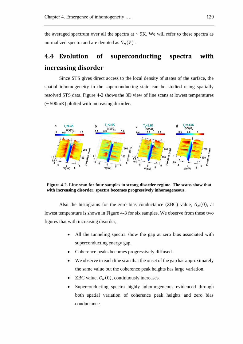
Chapter 4. Emergence of inhomogeneity …. 129
the averaged spectrum over all the spectra at ~ 9K. We will refer to these spectra as
normalized spectra and are denoted as 𝐺𝑁(𝑉) .
4.4 Evolution of superconducting spectra with
increasing disorder
Since STS gives direct access to the local density of states of the surface, the
spatial inhomogeneity in the superconducting state can be studied using spatially
resolved STS data. Figure 4-2 shows the 3D view of line scans at lowest temperatures
(~ 500mK) plotted with increasing disorder.
b
dc
V(mV)V(mV)V(mV)
0 0
0.6 0.8 1
0.5-5
5
200
100
G(V)/GN
Po
sit
ion
(n
m)
Po
sit
ion
(n
m)
Po
sit
ion
(n
m)
G(V)/GN
G(V)/GN
0
100
200
0
100
200
0-55
0-55
1
0.4 1.20.81.60.5 1
12
0.4
1.20.8
a
0
0.2
TC=1.65KT
C=2.9KT
C=3.5K
0 0.5G(V)/G
N
V(mV)0 0
-55
200
100
Po
sit
ion
(n
m)
1.51
0.61.2
0
TC=6.4K
Figure 4-2. Line scan for four samples in strong disorder regime. The scans show that
with increasing disorder, spectra becomes progressively inhomogeneous.
Also the histograms for the zero bias conductance (ZBC) value, 𝐺𝑁(0), at
lowest temperature is shown in Figure 4-3 for six samples. We observe from these two
figures that with increasing disorder,
All the tunneling spectra show the gap at zero bias associated with
superconducting energy gap.
Coherence peaks becomes progressively diffused.
We observe in each line scan that the onset of the gap has approximately
the same value but the coherence peak heights has large variation.
ZBC value, 𝐺𝑁(0), continuously increases.
Superconducting spectra highly inhomogeneous evidenced through
both spatial variation of coherence peak heights and zero bias
conductance.
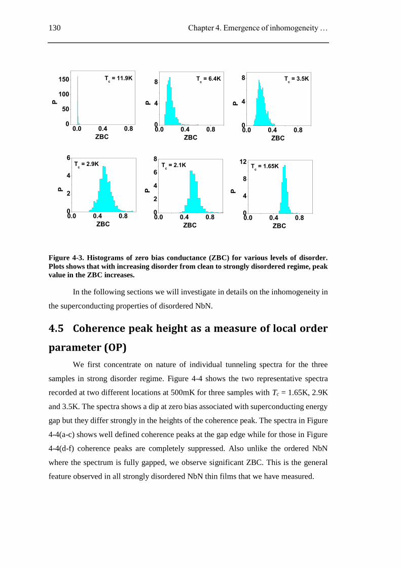
130 Chapter 4. Emergence of inhomogeneity …
0.0 0.4 0.80
50
100
150
P
ZBC
Tc = 11.9K T
c = 6.4K T
c = 3.5K
Tc = 1.65KT
c = 2.1KT
c = 2.9K
0.0 0.4 0.80
4
8
P
ZBC0.0 0.4 0.80
4
8
P
ZBC
0.0 0.4 0.80
2
4
6
P
ZBC0.0 0.4 0.80
2
4
6
8
P
ZBC0.0 0.4 0.80
4
8
12
PZBC
Figure 4-3. Histograms of zero bias conductance (ZBC) for various levels of disorder.
Plots shows that with increasing disorder from clean to strongly disordered regime, peak
value in the ZBC increases.
In the following sections we will investigate in details on the inhomogeneity in
the superconducting properties of disordered NbN.
4.5 Coherence peak height as a measure of local order
parameter (OP)
We first concentrate on nature of individual tunneling spectra for the three
samples in strong disorder regime. Figure 4-4 shows the two representative spectra
recorded at two different locations at 500mK for three samples with Tc = 1.65K, 2.9K
and 3.5K. The spectra shows a dip at zero bias associated with superconducting energy
gap but they differ strongly in the heights of the coherence peak. The spectra in Figure
4-4(a-c) shows well defined coherence peaks at the gap edge while for those in Figure
4-4(d-f) coherence peaks are completely suppressed. Also unlike the ordered NbN
where the spectrum is fully gapped, we observe significant ZBC. This is the general
feature observed in all strongly disordered NbN thin films that we have measured.
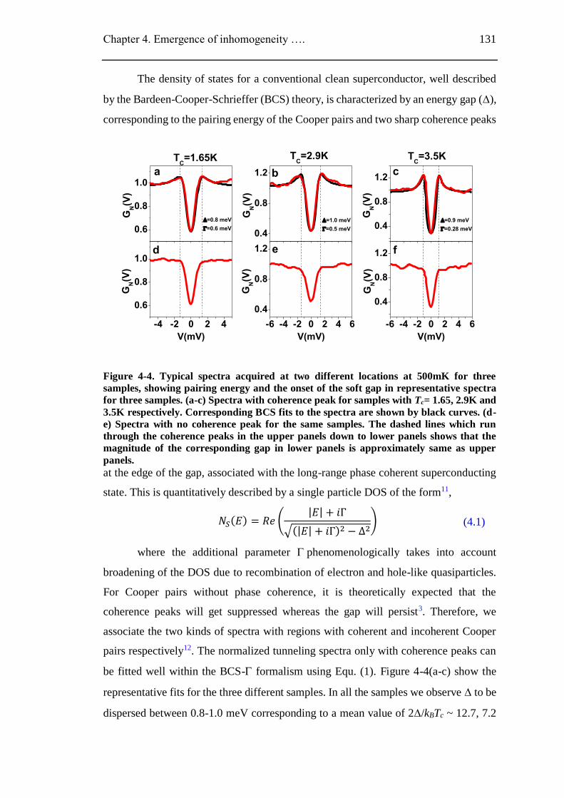
Chapter 4. Emergence of inhomogeneity …. 131
The density of states for a conventional clean superconductor, well described
by the Bardeen-Cooper-Schrieffer (BCS) theory, is characterized by an energy gap (),
corresponding to the pairing energy of the Cooper pairs and two sharp coherence peaks
0.6
0.8
1.0
-4 -2 0 2 4
0.6
0.8
1.0
0.4
0.8
1.2
-6 -4 -2 0 2 4 6
0.4
0.8
1.2
0.4
0.8
1.2
-6 -4 -2 0 2 4 6
0.4
0.8
1.2 fed
b c
TC=3.5KT
C=2.9K
=0.8 meV
=0.6 meV
GN(V
)
TC=1.65K
a
GN(V
)
V(mV)
=1.0 meV
=0.5 meV
GN(V
)
GN(V
)
V(mV)
=0.9 meV
=0.28 meV
GN(V
)
GN(V
)
V(mV)
Figure 4-4. Typical spectra acquired at two different locations at 500mK for three
samples, showing pairing energy and the onset of the soft gap in representative spectra
for three samples. (a-c) Spectra with coherence peak for samples with Tc= 1.65, 2.9K and
3.5K respectively. Corresponding BCS fits to the spectra are shown by black curves. (d-
e) Spectra with no coherence peak for the same samples. The dashed lines which run
through the coherence peaks in the upper panels down to lower panels shows that the
magnitude of the corresponding gap in lower panels is approximately same as upper
panels.
at the edge of the gap, associated with the long-range phase coherent superconducting
state. This is quantitatively described by a single particle DOS of the form11,
𝑁𝑆(𝐸) = 𝑅𝑒 (|𝐸| + 𝑖Γ
√(|𝐸| + 𝑖Γ)2 − Δ2) (4.1)
where the additional parameter phenomenologically takes into account
broadening of the DOS due to recombination of electron and hole-like quasiparticles.
For Cooper pairs without phase coherence, it is theoretically expected that the
coherence peaks will get suppressed whereas the gap will persist3. Therefore, we
associate the two kinds of spectra with regions with coherent and incoherent Cooper
pairs respectively12. The normalized tunneling spectra only with coherence peaks can
be fitted well within the BCS- formalism using Equ. (1). Figure 4-4(a-c) show the
representative fits for the three different samples. In all the samples we observe to be
dispersed between 0.8-1.0 meV corresponding to a mean value of 2/kBTc ~ 12.7, 7.2
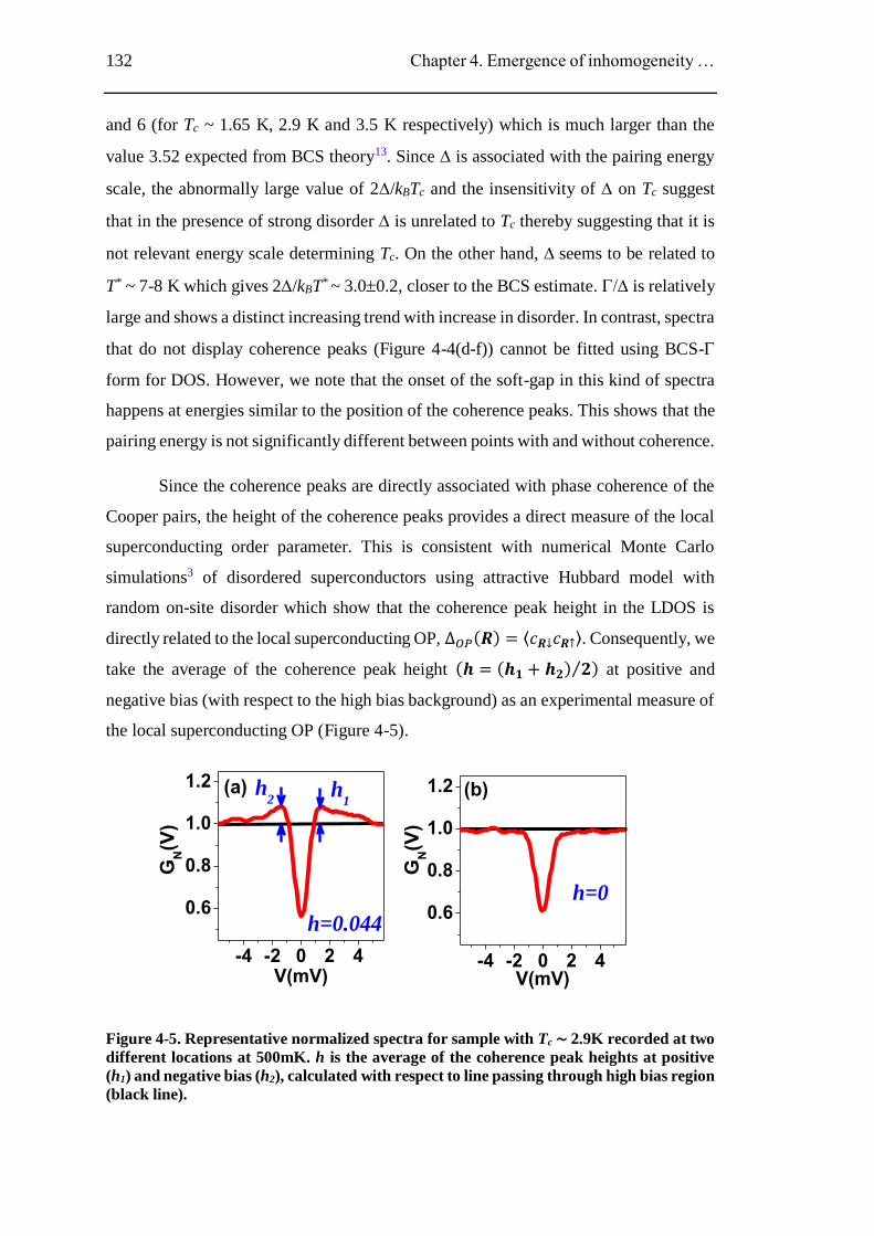
132 Chapter 4. Emergence of inhomogeneity …
and 6 (for Tc ~ 1.65 K, 2.9 K and 3.5 K respectively) which is much larger than the
value 3.52 expected from BCS theory13. Since is associated with the pairing energy
scale, the abnormally large value of 2/kBTc and the insensitivity of on Tc suggest
that in the presence of strong disorder is unrelated to Tc thereby suggesting that it is
not relevant energy scale determining Tc. On the other hand, seems to be related to
T* ~ 7-8 K which gives 2/kBT* ~ 3.00.2, closer to the BCS estimate. is relatively
large and shows a distinct increasing trend with increase in disorder. In contrast, spectra
that do not display coherence peaks (Figure 4-4(d-f)) cannot be fitted using BCS-
form for DOS. However, we note that the onset of the soft-gap in this kind of spectra
happens at energies similar to the position of the coherence peaks. This shows that the
pairing energy is not significantly different between points with and without coherence.
Since the coherence peaks are directly associated with phase coherence of the
Cooper pairs, the height of the coherence peaks provides a direct measure of the local
superconducting order parameter. This is consistent with numerical Monte Carlo
simulations3 of disordered superconductors using attractive Hubbard model with
random on-site disorder which show that the coherence peak height in the LDOS is
directly related to the local superconducting OP, Δ𝑂𝑃(𝑹) = ⟨𝑐𝑹↓𝑐𝑹↑⟩. Consequently, we
take the average of the coherence peak height (𝒉 = (𝒉𝟏 + 𝒉𝟐) 𝟐⁄ ) at positive and
negative bias (with respect to the high bias background) as an experimental measure of
the local superconducting OP (Figure 4-5).
-4 -2 0 2 4
0.6
0.8
1.0
1.2
-4 -2 0 2 4
0.6
0.8
1.0
1.2h1
GN(V
)
V(mV)
h=0.044
h2
(a) (b)
h=0
V(mV)
GN(V
)
Figure 4-5. Representative normalized spectra for sample with Tc ∼ 2.9K recorded at two
different locations at 500mK. h is the average of the coherence peak heights at positive
(h1) and negative bias (h2), calculated with respect to line passing through high bias region
(black line).
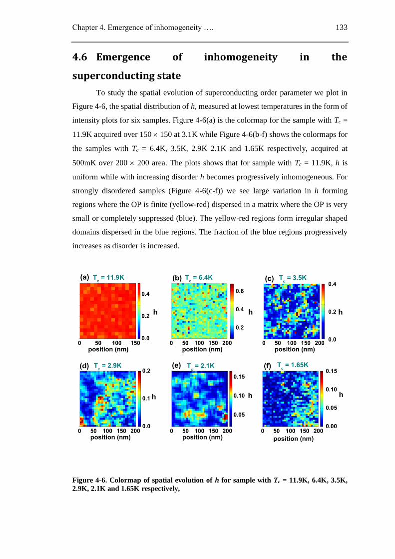
Chapter 4. Emergence of inhomogeneity …. 133
4.6 Emergence of inhomogeneity in the
superconducting state
To study the spatial evolution of superconducting order parameter we plot in
Figure 4-6, the spatial distribution of h, measured at lowest temperatures in the form of
intensity plots for six samples. Figure 4-6(a) is the colormap for the sample with Tc =
11.9K acquired over 150 150 at 3.1K while Figure 4-6(b-f) shows the colormaps for
the samples with Tc = 6.4K, 3.5K, 2.9K 2.1K and 1.65K respectively, acquired at
500mK over 200 200 area. The plots shows that for sample with Tc = 11.9K, h is
uniform while with increasing disorder h becomes progressively inhomogeneous. For
strongly disordered samples (Figure 4-6(c-f)) we see large variation in h forming
regions where the OP is finite (yellow-red) dispersed in a matrix where the OP is very
small or completely suppressed (blue). The yellow-red regions form irregular shaped
domains dispersed in the blue regions. The fraction of the blue regions progressively
increases as disorder is increased.
0 50 100 150 2000.00
0.05
0.10
0.15
0 50 100 150 2000.0
0.1
0.2
0 50 100 150 2000.0
0.2
0.4
0 50 100 1500.0
0.2
0.4
0 50 100 150 200
0.2
0.4
0.6
0 50 100 150 200
0.05
0.10
0.15
Tc = 1.65KT
c = 2.1KT
c = 2.9K
Tc = 3.5KT
c = 6.4KT
c = 11.9K
(f)(e)(d)
(c)(b)
position (nm)
(a)
h
position (nm)
hhh
h
position (nm)
position (nm)
h
position (nm)
position (nm)
Figure 4-6. Colormap of spatial evolution of h for sample with Tc = 11.9K, 6.4K, 3.5K,
2.9K, 2.1K and 1.65K respectively,
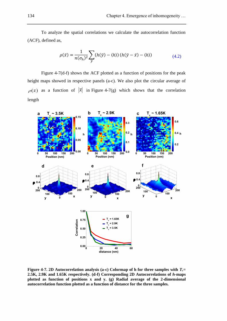
134 Chapter 4. Emergence of inhomogeneity …
To analyze the spatial correlations we calculate the autocorrelation function
(ACF), defined as,
𝜌(�̅�) =1
𝑛(𝜎ℎ)2∑(ℎ(�̅�) − ⟨ℎ⟩)
�̅�
(ℎ(�̅� − �̅�) − ⟨ℎ⟩) (4.2)
Figure 4-7(d-f) shows the ACF plotted as a function of positions for the peak
height maps showed in respective panels (a-c). We also plot the circular average of
x as a function of x in Figure 4-7(g) which shows that the correlation
length
0 20 40 600.00
0.25
0.50
0.75
1.00
0 50 100 150 2000.00
0.05
0.10
0.15
fed
yyy xx
000
0.80.8 0.8
0.40.40.4
00
100100
100100100
200200
200200 200200
100
h
Position (nm)
0 x
0 50 100 150 2000.0
0.1
0.2
0.3
cb Tc ~ 1.65KT
c ~ 2.9K
h
Position (nm)
Tc ~ 3.5Ka
0 50 100 150 200
0.2
0.4
0.6
h
Position (nm)
Tc = 1.65K
Tc = 2.9K
Tc = 3.5K
g
distance (nm)
Co
rre
lati
on
Figure 4-7. 2D Autocorrelation analysis (a-c) Colormap of h for three samples with Tc=
2.5K, 2.9K and 1.65K respectively. (d-f) Corresponding 2D Autocorrelations of h-maps
plotted as function of positions x and y. (g) Radial average of the 2-dimensional
autocorrelation function plotted as a function of distance for the three samples.
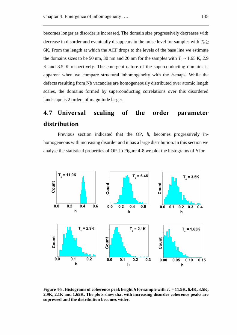
Chapter 4. Emergence of inhomogeneity …. 135
becomes longer as disorder is increased. The domain size progressively decreases with
decrease in disorder and eventually disappears in the noise level for samples with Tc≥
6K. From the length at which the ACF drops to the levels of the base line we estimate
the domains sizes to be 50 nm, 30 nm and 20 nm for the samples with Tc ~ 1.65 K, 2.9
K and 3.5 K respectively. The emergent nature of the superconducting domains is
apparent when we compare structural inhomogeneity with the h-maps. While the
defects resulting from Nb vacancies are homogeneously distributed over atomic length
scales, the domains formed by superconducting correlations over this disordered
landscape is 2 orders of magnitude larger.
4.7 Universal scaling of the order parameter
distribution
Previous section indicated that the OP, h, becomes progressively in-
homogeneous with increasing disorder and it has a large distribution. In this section we
analyse the statistical properties of OP. In Figure 4-8 we plot the histograms of h for
0.0 0.2 0.4 0.6
Tc = 1.65KT
c = 2.1KT
c = 2.9K
Tc = 3.5KT
c = 6.4K
Co
un
t
h
Tc = 11.9K
0.0 0.2 0.4 0.6
Co
un
t
h0.0 0.1 0.2 0.3 0.4
Co
un
t
h
0.0 0.1 0.2
Co
un
t
h0.0 0.1 0.2 0.3
Co
un
t
h0.00 0.05 0.10 0.15
Co
un
t
h
Figure 4-8. Histograms of coherence peak height h for sample with Tc = 11.9K, 6.4K, 3.5K,
2.9K, 2.1K and 1.65K. The plots show that with increasing disorder coherence peaks are
supressed and the distribution becomes wider.
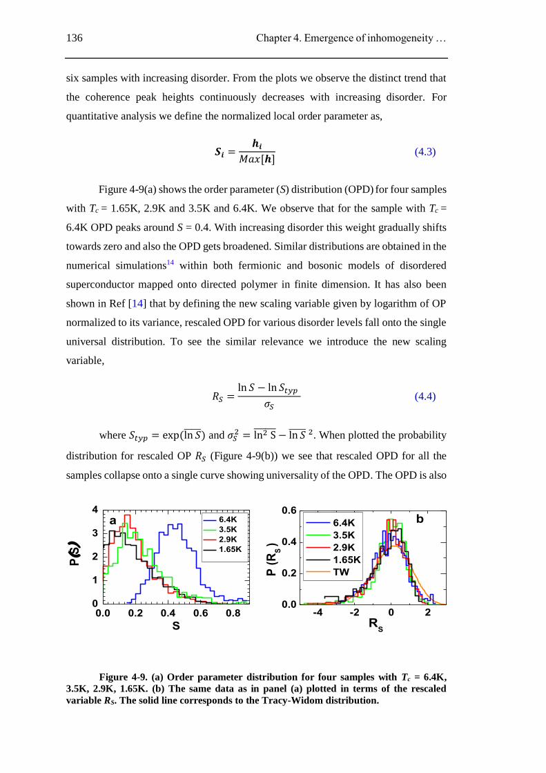
136 Chapter 4. Emergence of inhomogeneity …
six samples with increasing disorder. From the plots we observe the distinct trend that
the coherence peak heights continuously decreases with increasing disorder. For
quantitative analysis we define the normalized local order parameter as,
𝑺𝒊 =𝒉𝒊
𝑀𝑎𝑥[𝒉] (4.3)
Figure 4-9(a) shows the order parameter (S) distribution (OPD) for four samples
with Tc = 1.65K, 2.9K and 3.5K and 6.4K. We observe that for the sample with Tc =
6.4K OPD peaks around S = 0.4. With increasing disorder this weight gradually shifts
towards zero and also the OPD gets broadened. Similar distributions are obtained in the
numerical simulations14 within both fermionic and bosonic models of disordered
superconductor mapped onto directed polymer in finite dimension. It has also been
shown in Ref [14] that by defining the new scaling variable given by logarithm of OP
normalized to its variance, rescaled OPD for various disorder levels fall onto the single
universal distribution. To see the similar relevance we introduce the new scaling
variable,
𝑅𝑆 =ln 𝑆 − ln 𝑆𝑡𝑦𝑝
𝜎𝑆 (4.4)
where 𝑆𝑡𝑦𝑝 = exp (ln 𝑆̅̅ ̅̅ ̅) and 𝜎𝑆2 = ln2 S̅̅ ̅̅ ̅̅ − ln 𝑆̅̅ ̅̅ ̅ 2. When plotted the probability
distribution for rescaled OP 𝑅𝑆 (Figure 4-9(b)) we see that rescaled OPD for all the
samples collapse onto a single curve showing universality of the OPD. The OPD is also
0.0 0.2 0.4 0.6 0.80
1
2
3
4 6.4K
3.5K
2.9K
1.65K
S
P(S)
-4 -2 0 20.0
0.2
0.4
0.6
6.4K
3.5K
2.9K
1.65K
TW
RS
P (
RS
)
a b
Figure 4-9. (a) Order parameter distribution for four samples with Tc = 6.4K,
3.5K, 2.9K, 1.65K. (b) The same data as in panel (a) plotted in terms of the rescaled
variable RS. The solid line corresponds to the Tracy-Widom distribution.
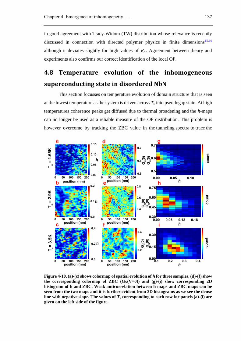
Chapter 4. Emergence of inhomogeneity …. 137
in good agreement with Tracy-Widom (TW) distribution whose relevance is recently
discussed in connection with directed polymer physics in finite dimensions15,16
although it deviates slightly for high values of 𝑅𝑆. Agreement between theory and
experiments also confirms our correct identification of the local OP.
4.8 Temperature evolution of the inhomogeneous
superconducting state in disordered NbN
This section focusses on temperature evolution of domain structure that is seen
at the lowest temperature as the system is driven across Tc into pseudogap state. At high
temperatures coherence peaks get diffused due to thermal broadening and the h-maps
can no longer be used as a reliable measure of the OP distribution. This problem is
however overcome by tracking the ZBC value in the tunneling spectra to trace the
0 50 100 150 2000.00
0.05
0.10
0.15
0 50 100 150 200
0.5
0.6
0.7
0.00 0.05 0.10
0.5
0.6
0.7
0 50 100 150 2000.0
0.1
0.2
0 50 100 150 200
0.4
0.6
0.8
0.00 0.06 0.12 0.180.30
0.45
0.60
0.75
0 50 100 150 2000.0
0.2
0.4
0 50 100 150 200
0.2
0.4
0.1 0.2 0.3 0.40.00
0.15
0.30
position (nm)
position (nm)
GN(0
)
h
GN(0
)
co
un
t
position (nm)
i
h
g
f
e
d
c
b
position (nm)
GN(0
)
a
h
GN(0
)
co
un
t
position (nm)
h
position (nm)
GN(0
)
Tc=
3.5
KT
c =
2.9
K
h
h
h
GN(0
)
co
un
t
Tc =
1.6
5K
Figure 4-10. (a)-(c) shows colormap of spatial evolution of h for three samples, (d)-(f) show
the corresponding colormap of ZBC (GN(V=0)) and (g)-(i) show corresponding 2D
histogram of h and ZBC. Weak anticorrelation between h maps and ZBC maps can be
seen from the two maps and it is further evident from 2D histograms as we see the dense
line with negative slope. The values of Tc corresponding to each row for panels (a)-(i) are
given on the left side of the figure.
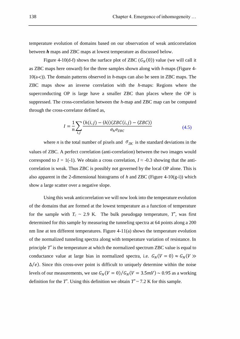
138 Chapter 4. Emergence of inhomogeneity …
temperature evolution of domains based on our observation of weak anticorrelation
between h maps and ZBC maps at lowest temperature as discussed below.
Figure 4-10(d-f) shows the surface plot of ZBC (𝐺𝑁(0)) value (we will call it
as ZBC maps here onward) for the three samples shown along with h-maps (Figure 4-
10(a-c)). The domain patterns observed in h-maps can also be seen in ZBC maps. The
ZBC maps show an inverse correlation with the h-maps: Regions where the
superconducting OP is large have a smaller ZBC than places where the OP is
suppressed. The cross-correlation between the h-map and ZBC map can be computed
through the cross-correlator defined as,
𝐼 =1
𝑛∑
(ℎ(𝑖, 𝑗) − ⟨ℎ⟩)(𝑍𝐵𝐶(𝑖, 𝑗) − ⟨𝑍𝐵𝐶⟩)
𝜎ℎ𝜎𝑍𝐵𝐶𝑖,𝑗
(4.5)
where n is the total number of pixels and ZBC is the standard deviations in the
values of ZBC. A perfect correlation (anti-correlation) between the two images would
correspond to I = 1(-1). We obtain a cross correlation, I ≈ -0.3 showing that the anti-
correlation is weak. Thus ZBC is possibly not governed by the local OP alone. This is
also apparent in the 2-dimensional histograms of h and ZBC (Figure 4-10(g-i)) which
show a large scatter over a negative slope.
Using this weak anticorrelation we will now look into the temperature evolution
of the domains that are formed at the lowest temperature as a function of temperature
for the sample with Tc ~ 2.9 K. The bulk pseudogap temperature, T*, was first
determined for this sample by measuring the tunneling spectra at 64 points along a 200
nm line at ten different temperatures. Figure 4-11(a) shows the temperature evolution
of the normalized tunneling spectra along with temperature variation of resistance. In
principle T* is the temperature at which the normalized spectrum ZBC value is equal to
conductance value at large bias in normalized spectra, i.e. 𝐺𝑁(𝑉 = 0) ≈ 𝐺𝑁(𝑉 ≫
∆ 𝑒⁄ ). Since this cross-over point is difficult to uniquely determine within the noise
levels of our measurements, we use 𝐺𝑁(𝑉 = 0) 𝐺𝑁(𝑉 = 3.5𝑚𝑉)⁄ ~ 0.95 as a working
definition for the T*. Using this definition we obtain T* ~ 7.2 K for this sample.
Chapter 4. Emergence of inhomogeneity …. 139
Spectroscopic maps were subsequently acquired at 6 different temperatures
over the same area as the one in Figure 4-10(e). Before acquiring the spectroscopic map
we corrected for the small drift using the topographic image, such that the maps were
0 50 100 150 200
0.3
0.4
0.5
0.6
0 50 100 150 200
0.3
0.4
0.5
0.6
0.7
0 50 100 150 200
0.3
0.4
0.5
0.6
0.7
0 50 100 150 200
0.4
0.6
0.8
0 50 100 150 200
0.6
0.8
1.0
0 50 100 150 200
0.6
0.8
1.0
GN(0)G
N(0)G
N(0)
GN(0)G
N(0)c
position (nm)
GN(0)
a
position (nm)
position (nm)
position (nm)
b
position (nm)
6.9K3.6K2.2K
1.7K1K
gfe
d
position (nm)
500mK
2 4 6
-2
0
2
T*=7.2KTC=2.9K
a)
V (
mV
)
T (K)
R(
)
0
100
200
300
0.6 0.8 1.0
GN(V)
Figure 4-11. Temperature evolution of the inhomogeneous superconducting state for the
sample with Tc = 2.9K. (a) Temperature evolution of spatially averaged normalized
tunneling spectra plotted in the form of intensity plot of GN(V) as a function of bias voltage
and temperature. Resistance vs temperature (R-T) for the same sample is shown in white
curve on the same plot. Pseudogap temperature T* ~ 7.2 K is marked with the dotted
black line on top of the plot. (b)-(g) Spatial variation of ZBC (GN(V=0)) plotted in the
form of intensity plot over the same area for six different temperatures.
taken over the same area at every temperature. Figure 4-11(b-g) show the ZBC maps
as a function of temperature. Below Tc, the domain pattern does not show a significant
change and for all points 𝐺𝑁(𝑉 = 0) 𝐺𝑁(𝑉 = 3.5𝑚𝑁)⁄ < 1 showing that a soft gap is
present everywhere. As the sample is heated across Tc Most of these domains continue
to survive at 3.6K across the superconducting transition. Barring few isolated points
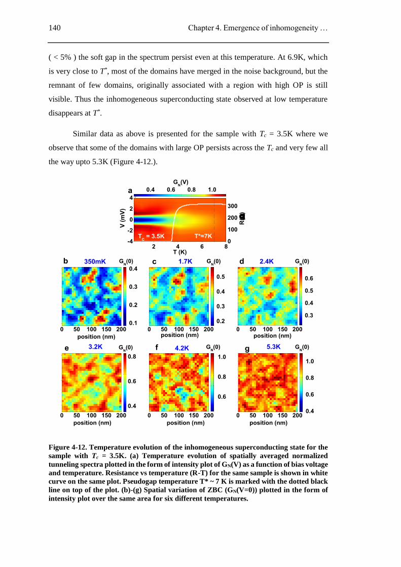
140 Chapter 4. Emergence of inhomogeneity …
( < 5% ) the soft gap in the spectrum persist even at this temperature. At 6.9K, which
is very close to T*, most of the domains have merged in the noise background, but the
remnant of few domains, originally associated with a region with high OP is still
visible. Thus the inhomogeneous superconducting state observed at low temperature
disappears at T*.
Similar data as above is presented for the sample with Tc = 3.5K where we
observe that some of the domains with large OP persists across the Tc and very few all
the way upto 5.3K (Figure 4-12.).
0 50 100 150 2000.1
0.2
0.3
0.4
0 50 100 150 200
0.2
0.3
0.4
0.5
0 50 100 150 200
0.3
0.4
0.5
0.6
0 50 100 150 200
0.4
0.6
0.8
0 50 100 150 200
0.6
0.8
1.0
0 50 100 150 2000.4
0.6
0.8
1.0
GN(0)G
N(0)G
N(0)
GN(0)G
N(0)c
position (nm)
GN(0)
a
position (nm)
position (nm)
position (nm)
b
position (nm)
5.3K4.2K3.2K
2.4K1.7K
gfe
d
position (nm)
350mK
2 4 6 8-4
-2
0
2
4
T*=7KTC = 3.5K
a)
V (
mV
)
T (K)
R(
)0
100
200
300
0.4 0.6 0.8 1.0
GN(V)
Figure 4-12. Temperature evolution of the inhomogeneous superconducting state for the
sample with Tc = 3.5K. (a) Temperature evolution of spatially averaged normalized
tunneling spectra plotted in the form of intensity plot of GN(V) as a function of bias voltage
and temperature. Resistance vs temperature (R-T) for the same sample is shown in white
curve on the same plot. Pseudogap temperature T* ~ 7 K is marked with the dotted black
line on top of the plot. (b)-(g) Spatial variation of ZBC (GN(V=0)) plotted in the form of
intensity plot over the same area for six different temperatures.
Chapter 4. Emergence of inhomogeneity …. 141
4.9 Discussion
We now discuss the implication of our results on the nature of the
superconducting transition. In a clean conventional superconductor the
superconducting transition, well described through BCS theory, is governed by a single
energy scale, which represent the pairing energy of the Cooper pairs. Consequently,
Tc is given by the temperature where ∆→ 0 This is indeed the case for NbN thin films
in the clean limit. On the other hand in the strong disorder limit, the persistence of the
gap in the single particle energy spectrum in the pseudogap state and the insensitivity
of on Tc conclusively establishes that is no longer the energy scale driving the
superconducting transition. Indeed, the formation of an inhomogeneous
superconducting state supports the notion that the superconducting state should be
visualized as a disordered network of superconducting islands where global phase
coherence is established below Tc through Josephson tunneling between
superconducting islands. Consequently at Tc, the phase coherence would get destroyed
through thermal phase fluctuations between the superconducting domains, while
coherent and incoherent Cooper pairs would continue to survive as evidenced from the
persistence of the domain structure and the soft gap in the tunneling spectrum at
temperatures above Tc. Finally, at T* we reach the energy scale set by the pairing energy
where the domain structure and the soft gap disappears.
This picture is further supported by measurements of the superfluid phase
stiffness (J) performed through low frequency penetration depth17 and high frequency
complex conductivity ( 'i” )18 on similar NbN samples. Low frequency
measurements reveal that in the same range of disorder where the pseudogap appears
( Tc ≤ 6K), J(T0) becomes a lower energy scale compared to ∆(0) (See Chapter 3
Figure 9)High frequency microwave measurements reveal that in the pseudogap
regime the superfluid stiffness becomes strongly frequency dependent. While at low
frequencies J ( ”) becomes zero close to Tc showing that the global phase
coherent state is destroyed, at higher frequencies J continues to remain finite up to a
higher temperature (Figure 4-13), which coincides with T* in the limit of very high
frequencies. Since the probing length scale set by the electron diffusion length at
microwave frequencies18 is of the same order as the size of the domains observed in
STS, finite J at these frequencies implies that the phase stiffness continues to remains
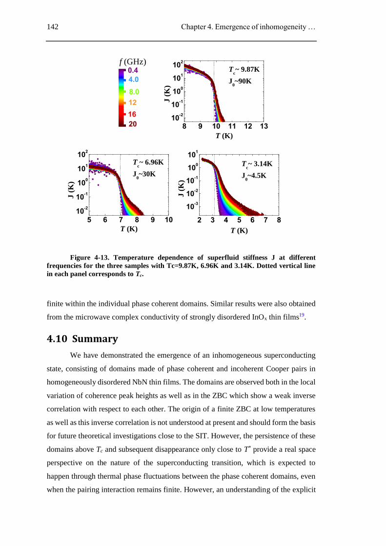
142 Chapter 4. Emergence of inhomogeneity …
5 6 7 8 9 1010
-2
10-1
100
101
102
2 3 4 5 6 7 8
10-3
10-2
10-1
100
101
8 9 10 11 12 1310
-2
10-1
100
101
102
J (
K)
T (K)
Tc~ 6.96K
J0~30K
Tc~ 3.14K
J0~4.5K
J (
K)
T (K)
f (GHz)0.4
4.0
8.0
12
16
20
J (
K)
T (K)
Tc~ 9.87K
J0~90K
Figure 4-13. Temperature dependence of superfluid stiffness J at different
frequencies for the three samples with Tc=9.87K, 6.96K and 3.14K. Dotted vertical line
in each panel corresponds to Tc.
finite within the individual phase coherent domains. Similar results were also obtained
from the microwave complex conductivity of strongly disordered InOx thin films19.
4.10 Summary
We have demonstrated the emergence of an inhomogeneous superconducting
state, consisting of domains made of phase coherent and incoherent Cooper pairs in
homogeneously disordered NbN thin films. The domains are observed both in the local
variation of coherence peak heights as well as in the ZBC which show a weak inverse
correlation with respect to each other. The origin of a finite ZBC at low temperatures
as well as this inverse correlation is not understood at present and should form the basis
for future theoretical investigations close to the SIT. However, the persistence of these
domains above Tc and subsequent disappearance only close to T* provide a real space
perspective on the nature of the superconducting transition, which is expected to
happen through thermal phase fluctuations between the phase coherent domains, even
when the pairing interaction remains finite. However, an understanding of the explicit
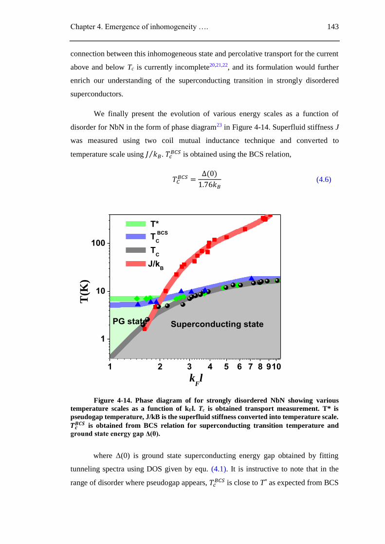
Chapter 4. Emergence of inhomogeneity …. 143
connection between this inhomogeneous state and percolative transport for the current
above and below Tc is currently incomplete20,21,22, and its formulation would further
enrich our understanding of the superconducting transition in strongly disordered
superconductors.
We finally present the evolution of various energy scales as a function of
disorder for NbN in the form of phase diagram23 in Figure 4-14. Superfluid stiffness J
was measured using two coil mutual inductance technique and converted to
temperature scale using 𝐽 𝑘𝐵⁄ . 𝑇𝑐𝐵𝐶𝑆 is obtained using the BCS relation,
𝑇𝐶𝐵𝐶𝑆 =
∆(0)
1.76𝑘𝐵 (4.6)
1 2 3 4 5 6 7 8 910
1
10
100
PG state
T(K
)
kFl
T*
T BCS
C
TC
J/kB
Superconducting state
Figure 4-14. Phase diagram of for strongly disordered NbN showing various
temperature scales as a function of kFl. Tc is obtained transport measurement. T* is
pseudogap temperature, J/kB is the superfluid stiffness converted into temperature scale.
𝑻𝒄𝑩𝑪𝑺 is obtained from BCS relation for superconducting transition temperature and
ground state energy gap Δ(0).
where Δ(0) is ground state superconducting energy gap obtained by fitting
tunneling spectra using DOS given by equ. (4.1). It is instructive to note that in the
range of disorder where pseudogap appears, 𝑇𝑐𝐵𝐶𝑆 is close to T* as expected from BCS
144 Chapter 4. Emergence of inhomogeneity …
theory. In the same range of disorder 𝐽 𝑘𝐵⁄ is smaller than 𝑇𝑐𝐵𝐶𝑆 showing that the
superconducting transition is governed by phase fluctuations. Our conclusion is that
energy scale determining T* is Δ(0) whereas the energy scale determining Tc minimum
of either of Δ(0) and 𝐽.
4.11 References
1 A.Ghosal, M. Randeria, and N. Trivedi, Role of Spatial Amplitude Fluctuations in
Highly Disordered s-Wave Superconductors, Phys. Rev. Lett. 81 3940 (1998)
2 Y. Dubi, Y. Meir and Y. Avishai, Nature of the superconductor–insulator transition
in disordered superconductors, Nature, 449 876 (2007)
3 Bouadim, K., Loh, Y. L., Randeria, M. & Trivedi, N. Single- and two-particle
energy gaps across the disorder-driven superconductor-insulator transition. Nat.
Phys. 7, 884-889 (2011).
4 Sambandamurthy, G., Engel, L. W., Johansson, A. and Shahar, D. Superconductivity
related insulating behaviour, Phys. Rev. Lett. 92, 107005 (2004).
5 Dubi, Y., Meir, Y., and Avishai, Y. Theory of the magnetoresistance of disordered
superconducting films. Phys. Rev. B 73 054509 (2006).
6 M. Mondal, A. Kamlapure, S. C. Ganguli, J. Jesudasan, V. Bagwe, L. Benfatto and
P. Raychaudhuri, Enhancement of the finite-frequency superfluid response in the
pseudogap regime of strongly disordered superconducting films, Scientific Reports 3,
1357 (2013)
Chapter 4. Emergence of inhomogeneity …. 145
7 Stewart Jr., M. D., Yin, A., Xu, J. M. and Valles Jr., J. M. Superconducting Pair
Correlations in an Amorphous Insulating Nanohoneycomb Film, Science 318, 1273
(2007).
8 Kopnov, G. et al. Little-Parks Oscillations in an Insulator. Phys. Rev. Lett. 109,
167002 (2012).
9 Wang, Z.L., Cowley, J.M. Simulating high-angle annular dark-field stem images
including inelastic thermal diffuse scattering. Ultramicroscopy 31, 437 (1989).
10 LeBeau, J.M., Findlay, S.D., Allen, L.J., Stemmer, S. Standardless Atom Counting
in Scanning Transmission Electron Microscopy, Nano Letters 10, 4405 (2010).
11 Dynes, R. C., Narayanamurti, V., and Garno, J. P. Direct Measurement of
Quasiparticle-Lifetime Broadening in a Strong-Coupled Superconductor, Phys. Rev.
Lett. 41, 1509 (1978).
12 Sacépé, B. et al., Localization of preformed Cooper pairs in disordered
superconductors. Nat. Phys. 7, 239-244 (2011).
13 Tinkham, M Introduction to Superconductivity (Dover Publications Inc., Mineola,
New York, 2004).
14 G. Lemarié, A. Kamlapure, D. Bucheli, L. Benfatto, J. Lorenzana, G. Seibold, S. C.
Ganguli, P. Raychaudhuri and C. Castellani, Universal scaling of the order-
parameter distribution in strongly disordered superconductors, Phys. Rev. B 85
184509 (2013)
15 C. Monthus and T. Garel, Random transverse field Ising model in dimensions d =
2,3: infinite disorder scaling via a non-linear transfer approach, J. Stat. Mech.:
Theory Exp. P01008 (2012)
16 C. Monthus and T. Garel, Random transverse field Ising model in dimension
d > 1: scaling analysis in the disordered phase from the directed polymer model, J.
Phys. A: Math. Theor. 45, 095002 (2012).
17 M. Mondal, A. Kamlapure, M. Chand, G. Saraswat, S. Kumar, J. Jesudasan, L.
Benfatto, V. Tripathi and P. Raychaudhuri, Phase fluctuations in a strongly
disordered s-wave NbN superconductor close to the Metal-Insulator transition, Phys.
Rev. Lett. 106, 047001 (2011).
18 M. Mondal, A. Kamlapure, S. C. Ganguli, J. Jesudasan, V. Bagwe, L. Benfatto and
P. Raychaudhuri, Enhancement of the finite-frequency superfluid response in the
pseudogap regime of strongly disordered superconducting films, Scientific Reports 3,
1357 (2013)
19 Liu, W., Kim, M., Sambandamurthy, G. and Armitage, N. P. Dynamical study of
phase fluctuations and their critical slowing down in amorphous superconducting
films. Phys. Rev. B 84, 024511(2011).
146 Chapter 4. Emergence of inhomogeneity …
20 Bucheli, D., Caprara, S., Castellani, C. and Grilli, M. Metal–superconductor
transition in low-dimensional superconducting clusters embedded in two-dimensional
electron systems. New Journal of Physics 15, 023014 (2013).
21 Li, Y., Vicente, C. L. and Yoon, J. Transport phase diagram for superconducting
thin films of tantalum with homogeneous disorder. Phys. Rev. B 81, 020505(R)
(2010).
22 Seibold, G., Benfatto, L., Castellani, C. & Lorenzana, J. Superfluid density and
phase relaxation in superconductors with strong disorder. Phys. Rev. Lett. 108,
207004 (2012).
23 A. Kamlapure, T. Das, S. C. Ganguli, J.B. Parmar, S. Bhattacharyya, P.
Raychaudhuri, Emergence of nanoscale inhomogeneity in the superconducting state
of a homogeneously disordered conventional superconductor, Scientific Reports 3,
2979 (2013).
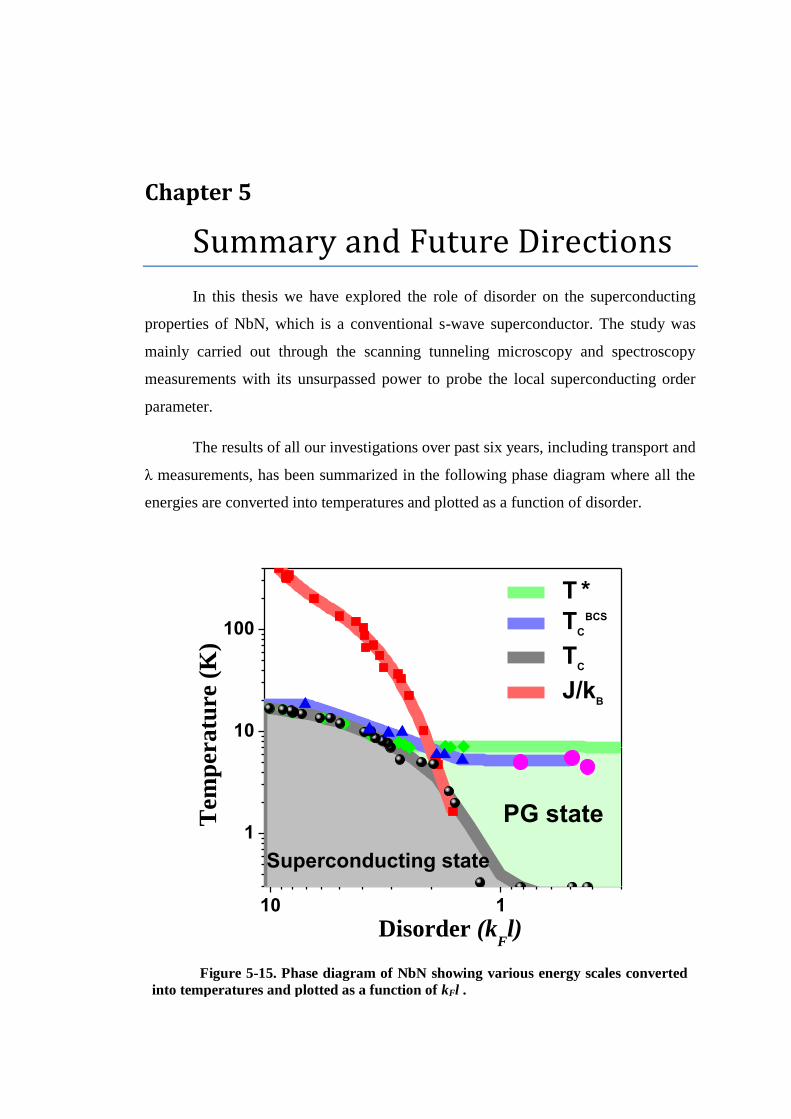
Chapter 5
Summary and Future Directions
In this thesis we have explored the role of disorder on the superconducting
properties of NbN, which is a conventional s-wave superconductor. The study was
mainly carried out through the scanning tunneling microscopy and spectroscopy
measurements with its unsurpassed power to probe the local superconducting order
parameter.
The results of all our investigations over past six years, including transport and
λ measurements, has been summarized in the following phase diagram where all the
energies are converted into temperatures and plotted as a function of disorder.
10 1
1
10
100
PG state
Tem
per
atu
re (
K)
Disorder (kFl)
T *
T BCS
C
TC
J/kB
Superconducting state
Figure 5-15. Phase diagram of NbN showing various energy scales converted
into temperatures and plotted as a function of kFl .
148 Chapter 5. Summary and Future directions
The critical temperature Tc represented by black circles1 decreases with
increasing disorder and becomes zero at 𝑘𝐹𝑙 ~ 1. Thus the zero resistance state is seen
in the half dome, shaded with grey colour and bounded by Tc line. The superfluid
stiffness, J/kB, is represented by red line2,3, decreases very rapidly with increasing
disorder. 𝑇𝑐𝐵𝐶𝑆 is the expected transition temperature calculated using the BCS relation4
∆(0) = 1.76𝑘𝐵𝑇𝐶𝐵𝐶𝑆.
In the intermediate disorder regime (𝑘𝐹𝑙 > 2.7), 𝐽 𝑘𝐵 > 𝑇𝑐𝐵𝐶𝑆⁄ and therefore
the transition in this regime is governed by vanishing of the energy gap as described by
BCS theory. We indeed see in the tunnelling spectra that the gap vanishes exactly where
the resistance appear and the spectra can be fitted with the BCS density of states for all
the temperatures.
In the strong disorder regime (𝑘𝐹𝑙 ≤ 2.7), 𝐽 𝑘𝐵 ≤ 𝑇𝑐𝐵𝐶𝑆⁄ and the formation of
pseudogap state, together indicates that here the superconductivity is suppressed
through phase fluctuations while the pairing remain finite all the way upto the
temperature T*. This scenario is further confirmed through the close resemblance of
𝑇𝑐𝐵𝐶𝑆 with the 𝑇∗.
For the strong disorder regime we proposed that the coherence peak height
represents a measure of the local order parameter (OP) and showed that it has universal
distribution irrespective of disorder strength. With this OP we observed the emergence
of inhomogeneous domains with large OP separated by regions of small OP. This
emergent inhomogeneity is seen over the length scale of few tens of nanometer while
the structural disorder is uniformly distributed over the atomic scale. We have also
demonstrated that these inhomogeneous domains that are formed at the lowest
temperature evolve smoothly with temperature across Tc and persists all the way upto
T*.
For 𝑘𝐹𝑙 < 1, MR data indicated the superconducting correlations persisting
upto the temperatures close to T* (Magenta circles), therefore it would be interesting to
explore this regime using STS to see whether the gap in the tunnelling spectra is also
seen5.
Finally it will be interesting to study spatially resolved STS measurements in
presence of magnetic field at various levels of disorder which will help us explore the
Chapter 5. Summary and Future directions 149
recent propositions6 on formation of superconducting island on the insulating side of
the SIT. This would ultimately help us understand better the nature of disordered driven
SIT.
References
1 M. Chand, G. Saraswat, A. Kamlapure, M. Mondal, S. Kumar, J. Jesudasan, V.
Bagwe, L. Benfatto, V. Tripathi, and P. Raychaudhuri, Phase diagram of a strongly
disordered s-wave superconductor, NbN, close to the metal-insulator transition. Phys.
Rev. B 85, 014508 (2012).
2 M. Mondal, A. Kamlapure, M. Chand, G. Saraswat, S. Kumar, J. Jesudasan, L.
Benfatto, V. Tripathi and P. Raychaudhuri, Phase fluctuations in a strongly
disordered s-wave NbN superconductor close to the Metal-Insulator transition, Phys.
Rev. Lett. 106, 047001 (2011).
3 M. Mondal, A. Kamlapure, S. C. Ganguli, J. Jesudasan, V. Bagwe, L. Benfatto and
P. Raychaudhuri, Enhancement of the finite-frequency superfluid response in the
pseudogap regime of strongly disordered superconducting films, Scientific Reports 3,
1357 (2013)
4 A. Kamlapure, T. Das, S. C. Ganguli, J.B. Parmar, S. Bhattacharyya, P.
Raychaudhuri, Emergence of nanoscale inhomogeneity in the superconducting state
of a homogeneously disordered conventional superconductor, Scientific Reports 3,
2979 (2013).
5 K. Bouadim, Y. L. Loh , M. Randeria, N. Trivedi, Single- and two-particle energy
gaps across the disorder-driven superconductor-insulator transition. Nat. Phys. 7,
884-889 (2011).
6 Y. Dubi, Y. Meir and Y. Avishai, Nature of the superconductor–insulator transition
in disordered superconductors, Nature, 449 876 (2007)


