

25. juni 2008
Silicon thinfilm tandem technology and industrial production by Sunfilm
Carsten Rohr
9 Jan. 2008

25.06.2008
Norsun
• Incorporated in 2005 as a subsidiary of Scatec • Manufactures mono-crystalline ingots and wafers• Mission to become the global cost- and technology leader in mono-crystalline wafers
production by 2010 • Shareholders: Scatec, Good Energies, Norsk Hydro, and others
Polysilicon Wafer Cells Modules Systems
Sunfilm AG
Polysilicon projects
Strategic partners
Okmetic
Equipment suppliers
Strategic partners
Investments
Partners

25.06.2008
PV grid price parity outlook
Average residential & commercial power price (Germany)
Peak utility price(Germany)
Source: Solarbuzz 2006, Citigroup 06/2005
Assumptions5% solar cost decline p.a.2.5% price increase p.a. of electricity tariff
Utility prices and solar power generation cost (EUR/kWh) in Germany (sun energy 900KWh/year)
0.0
0.2
0.4
0.6
0.8
2005 2010 2015 2020 2025 2030 2035 2040
Residential competitive
Commercial competitive
Utility bulk power priceAverage industrial power priceAverage commercial power priceAverage residential power price
Commercial Solar production costIndustrial Solar production cost
Residential Solar production cost
Solar production cost Utility prices
Residential systems
Commercial systems
Grid parity in certain markets

Solar cell technologies
Source: ThinFilm Sun&Wind Energy 1/2007, PSE 2007
Production in 2006 (in MWp)
n.a.
n.a.
n.a.
n.a.
n.a.
n.a.
Solar Cell
Crystalline Si Wafer
Amorphous + µc Si
Thin Film
Concentrator (III - V)
Mono Crystalline
Multi Crystalline
Ribbon
CdTe
CIS
Other Chalcopyrites
GaAs
InP
Others
New Technologies
Dye Solar Cell
Organic Structures
Others
Thin Film Crystalline
880
1089
57
153
n.a.
57
9
n.a.
1 GWp0
90%
Thin film advantages
+ Cost
+ No resource constraints
+ Scaling
+ New applications

25.06.2008
Cell / module production outlook
Source: averages from UBS, GS, Photon, LBBW (update 08.11.2007).
2,1 2,5 3,75,7
8,9
0,2 0,61,2
2,0
2,8
3,5
14,5
02468
101214161820
2006 2007 2008 2009 2010 2011
Thin filmConventional PV
GW
Thin film at ~19% market
share
Thin film at ~10% market
share
2.3 3.14.9
7.7
13.1
2006-2011 CAGRConventional PV: 47%Thin film: 77%Total: 51%
18.0

25. juni 2008
Announced production capacity by thinfilm technology
Source: Status and Perspectives of Thin Film Solar Cell Production, A. Jäger-Waldau, European Commission, DG JRC, Ispra, 22nd EU PVSEC, Milan 2007.

25.06.2008
Markets recognize thin film potential
Thin film: First Solar
Integrated: SolarWorld, REC and Trina
Cell / module: SunPower, Suntech, Q-Cells, Motech, Solarfun, Canadian Solar, Aleo Solar & Solon
500
450
400
350
300
250
200
150
100
50Nov 06 Jan 07 Apr 07 Jun 07 Aug 07 Nov 07
Thin film: 363%
Integrated: 129%
Cell / module: 99%
Silicon feedstock: 46%
MSCI Utilities: 16%Conglomerates: -13%
Indexed to 100
Source: Morgan Stanley, November 2007
Silicon feedstock: MEMC, Tokuyama and Wacker
Conglomerates: Sharp, Kyocera, BP, Energy Conversion and Sanyo
Thin film offers clear advantages• High potential for cost reduction• Low material costs (1% of Si use vs. wafer based techs) and no major
silicon constraints• Higher energy yield at less optimal environmental conditions
(dawn, dusk, cloudy days)– Performance advantage in northern locations– Performance advantage in hot climates (better temperature coefficient)– Generates ~10% more energy (kWh) per Watt peak installed than
crystalline PV• Strong synergies with flat panel display industry (=> industrial production)
25. juni 2008
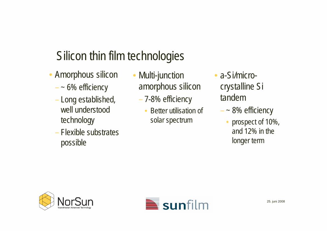
Silicon thin film technologies• Amorphous silicon
– ~ 6% efficiency– Long established,
well understood technology
– Flexible substrates possible
• Multi-junction amorphous silicon– 7-8% efficiency
• Better utilisation of solar spectrum
• a-Si/micro-crystalline Si tandem– ~ 8% efficiency
• prospect of 10%, and 12% in the longer term
25. juni 2008
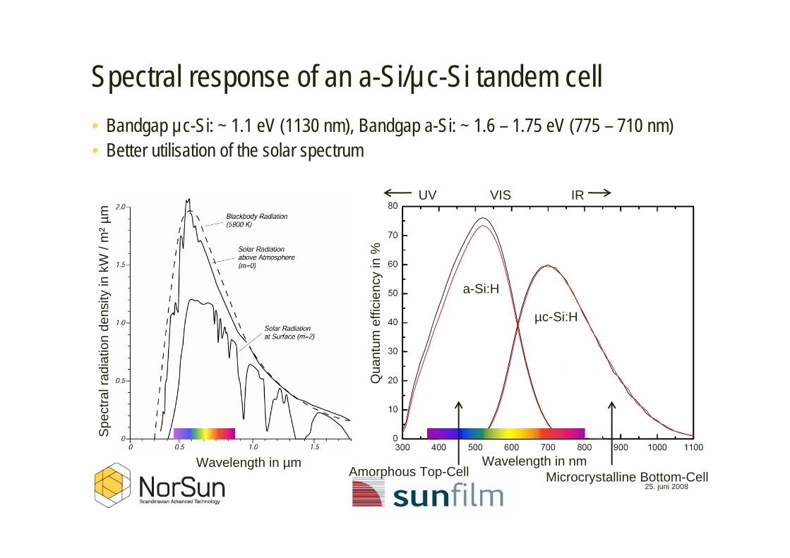
Amorphous Top-Cell Microcrystalline Bottom-Cell
Spectral response of an a-Si/µc-Si tandem cell• Bandgap µc-Si: ~ 1.1 eV (1130 nm), Bandgap a-Si: ~ 1.6 – 1.75 eV (775 – 710 nm)• Better utilisation of the solar spectrum
a-Si:H
µc-Si:H
Wavelength in nm
Qua
ntum
effi
cien
cyin
%
UV VIS IR
Wavelength in µm
Spe
ctra
l rad
iatio
n de
nsity
in k
W /
m²µ
m
25. juni 2008
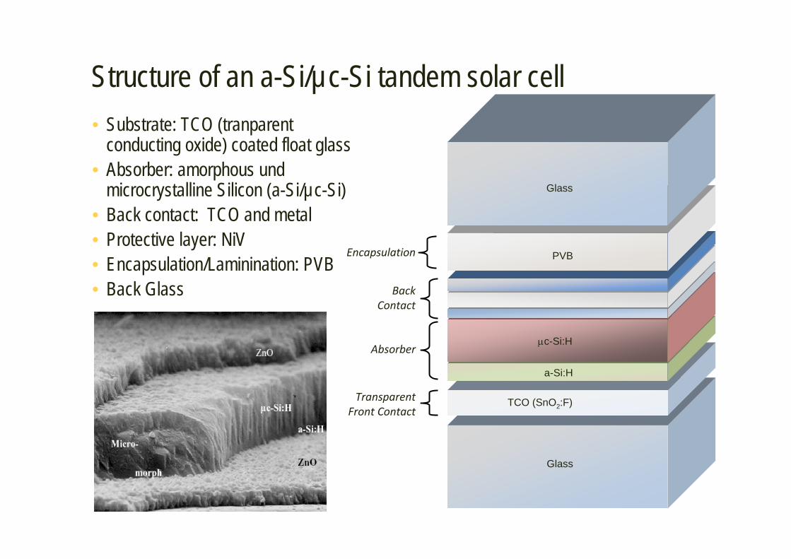
Structure of an a-Si/µc-Si tandem solar cell• Substrate: TCO (tranparent
conducting oxide) coated float glass• Absorber: amorphous und
microcrystalline Silicon (a-Si/µc-Si)• Back contact: TCO and metal• Protective layer: NiV• Encapsulation/Laminination: PVB• Back Glass
Glass
TCO (SnO2:F)
a-Si:H
μc-Si:H
PVB
Glass
Back Contact
Transparent Front Contact
Absorber
Encapsulation

25. juni 2008
Players in Silicon thinfilm PV• Equipment / technology
providers:– Applied Materials (USA)– Oerlikon (Switzerland)– Ulvac (Japan)
• Module manufacturers:– Kaneka (Japan)– Mitsubishi Heavy Industries (Japan)– Sharp (Japan)– Topray (China)– Brilliant 234 (Germany)– Sanyo (Japan)– Ersol (Germany)– Moser Baer (India)– T Solar Global (Spain)– Signet Solar (USA/India/Germany)– Sunfilm (Germany)– etc.

Applied Materials production line “Applied Sunfab”Quality
Deposition (TCO, back surface reflectors)
Junction Box Attach
Washing
Lasering
Lasering
Lamination
Back Glas
PECVD Deposition (Silicon layer)
Source: Applied Materials

25. juni 2008
PECVD - Plasma-enhanced chemical vapor deposition• Plasma to generate reactive
species via ionisation, dissociation and excitation
• Chemical reaction on heated substrate (~ 200°C)
• Process gases:• Silane (SiH4) and H2• TMB (Trimethylboran) for p-
doping• Phosphin (PH3) for n-doping
• Deposition rate• Influence on crystallinity
• Afterwards: • Cleaning with NF3• Purging with Ar
Silane
(SiH4)
Exhaust
RF-Generator (13.56 MHz)
Plasma
Diffuser
H2
Substrate Substrate heater
Electrode

25. juni 2008
PVD - Physical Vapor Deposition• Plasma to generate Ar+ ions• Low energy Ar+ ions are
accelerated to hit the target and thereby release atoms (sputter) which deposit on the substrate
• Sputter targets: metal, metal oxides
25. juni 2008
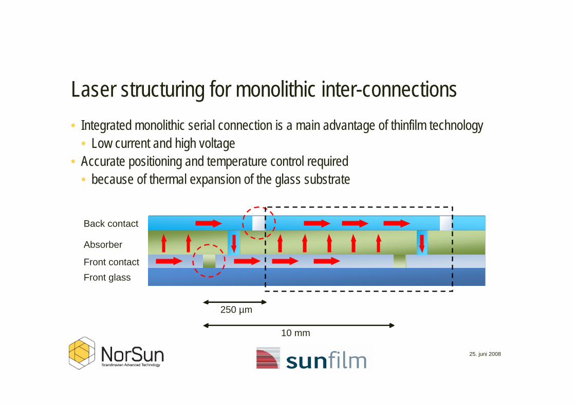
Front glassFront contact
Absorber
Back contact
Laser structuring for monolithic inter-connections• Integrated monolithic serial connection is a main advantage of thinfilm technology
• Low current and high voltage• Accurate positioning and temperature control required
• because of thermal expansion of the glass substrate
250 µm
10 mm

Sunfilm – Norsun investment in thin film
• based in Großröhrsdorf near Dresden (Germany) • first 60MWp factory is being built
• Construction started summer 2007 • Production expected to commence summer 2008• About 180 employees when fully operational
• Ambitious growth plans

Gen 8.5 Silicon thinfilm module• Size and flexibility• Low cost promise• Higher energy yield• Good aesthetics• Suited for Building
Integrated Photovoltaics (BIPV)
• No cadmium2.2
2.6
Gen 8.5
1.1
1.3
Gen 5
Monocrystalline Si module
Multicrystalline Si module
8% nominal 450Wp

Fab 1 currently under construction
Site Fab 1 purchased/ additional land blocked
Temporary offices
23km from Dresden
Gas farm and other expansion areas

May 2007

June 1, 2007 „ Groundbreaking“

August 12, 2007

August 20, 2007

November 8, 2007 „Topping“
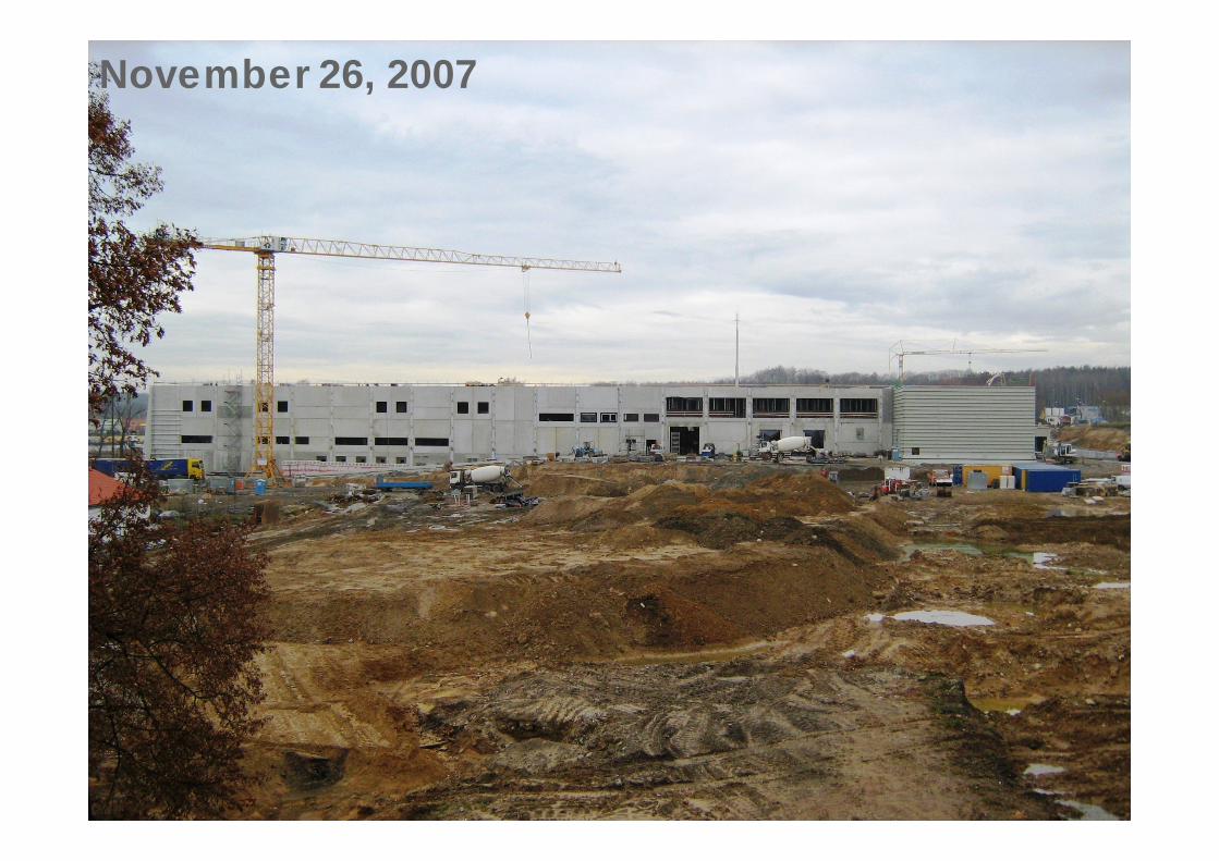
November 26, 2007

25.06.2008
December 10, 2007

25.06.2008
January 4, 2008

Sunfilm contactsWolfgang Heinze, COO
Dr. Sicco W.T. Westra, CBDO
Dr. Wilhelm Stein, Head of Process Technology
David Metzger, Member of the Executive Board
Sunfilm AG
Strasse E, Nr 8
01900 Grossröhrsdorf
Tel +49 35952 280 000
Fax +49 35952 280 111
www.sunfilmsolar.com
Dr. Carsten Rohr, Business Development, NorSun AS, [email protected]
www.norsuncorp.no


