

SOI Pixel Detector :
Present Status & Future PlansSuper Belle Collb. MtgDec. 11, 2008Yasuo Arai (KEK)[email protected]://rd.kek.jp/project/soi/
1
[SOI Pixel Collaboration]
• KEK : Y. Unno, S. Terada, Y. Ikegami, T. Tsuboyama, T. Kohriki, K. Tauchi, Y. Ikemoto, T. Miyoshi, Y. Arai
• U. of Tsukuba : K. Hara, H. Miyake, M. Kouchiyama, T. Sega
• Osaka U. : K. Hanagaki, M. Hirose
• JAXA/ISAS : H, Ikeda, D. Kobayashi, T. Wada, H. Nagata
• Tohoku U. : H. Yamamoto, Y. Takubo, T. Nagamine, Y. Horii, Y. Sato,
• Kyoto U. : T. Tsuru
• Riken/JASRI : T. Hatsui, T. Kudo, R. Ichimiya, A. Taketani
• U. of Hawaii : G. Varner, J. Kennedy, M. Cooney, H. Hoedlmoser, E. Martin
• LBNL : P. Denes, M. Battaglia, C. Vu, D. Contarato, P. Giubilato, L. Glesener
• FNAL : R. Yarema, R. Lipton, G. Deptuch, M. Trimpl
• OKI Elec. Ind. Co. Ltd. : M. Ohno, K. Fukuda, J. Ida, H. Hayashi, Y. Kawai, M. Okihara, H. Komatsubara, A. Ohtomo

OUTLINE
• Introduction of SOI Pixel R&D• SOI Pixel Test Results• R&D Plans• Summary
2

下部 Si をセンサーとして利用
Bonded wafer : High Resistivity (Sensor) + Low Resistivity (CMOS) .
Truly Monolithic Detector (-> High Density, Low material, Thin Device).
Standard CMOS can be used (-> Complex functions in a pixel).
No mechanical bonding (-> High yield, Low cost).
Fully depleted sensor with small capacitance of the sense node (~10fF, High conversion gain, Low noise)
Based on Industrial standard technology (-> Cost benefit and Scalability)
No Latch Up, Rad Hard.
Low Power
Low to High Temp(4K-300C) operation
...
Features of SOI Pixel Detector
3

KEK SOIPIX Target & Brief History
'05. 7: Start Collaboration with OKI Elec. Co. Ltd.
'05.10: TEG submission to OKI SOI 0.15 m process.
'06.12: 1st 0.15 um MPW run hosted by KEK.(17 designs; KEK, Japanese Universities, LBNL, FNAL, U of Hawaii)
'07.6: Process (and Fab.) is changed from 0.15 m to 0.2 m.
'08.1: 1st 0.2 um KEK MPW run is submitted.
'09.1: 2nd 0.2 um MPW run will be submitted.
'09.6: 3rd 0.2um MPW run is planned.
Starting as a generic R&D program of KEK Detector Technology project in 2005.Main purposes are to establish a SOI Pixel process and develop pixel detectors for many applications.
4
5
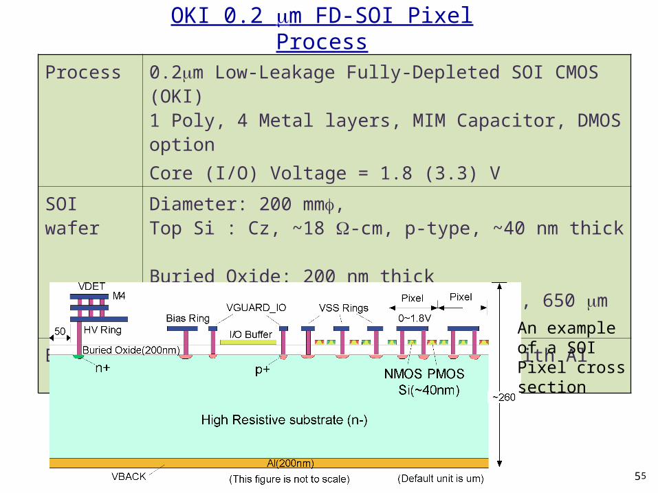
OKI 0.2 m FD-SOI Pixel Process
Process 0.2m Low-Leakage Fully-Depleted SOI CMOS (OKI)1 Poly, 4 Metal layers, MIM Capacitor, DMOS option
Core (I/O) Voltage = 1.8 (3.3) V
SOI wafer Diameter: 200 mm, Top Si : Cz, ~18 -cm, p-type, ~40 nm thick Buried Oxide: 200 nm thickHandle wafer: Cz 、 700 -cm (n-type), 650 m thick
Backside Thinned to 260 m, and sputtered with Al (200 nm).
An example of a SOI Pixel cross section
5
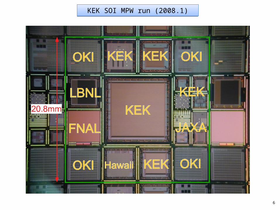
KEK SOI MPW run (2008.1)KEK SOI MPW run (2008.1)
6

77
Integration Type Pixel (INTPIX)
20 m x 20 m pixel20 m x 20 m pixel7
128 x 128 pixels5 x 5 mm2
128 x 128 pixels5 x 5 mm2

Counting Type Pixel
10.4 mm□128 x 128 pix10.4 mm□128 x 128 pix
ChargeAmp
DualDiscri Counter
Energy window and counting in each pixel.Energy window and counting in each pixel.
9
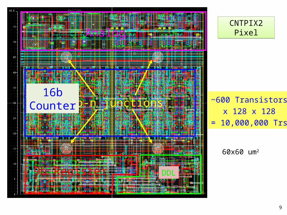
CNTPIX2 Pixel
CNTPIX2 Pixel
60x60 um2
~600 Transistors
x 128 x 128
= 10,000,000 Trs
p-n junctions
Analog
16bCounter
9b Register DDL
10
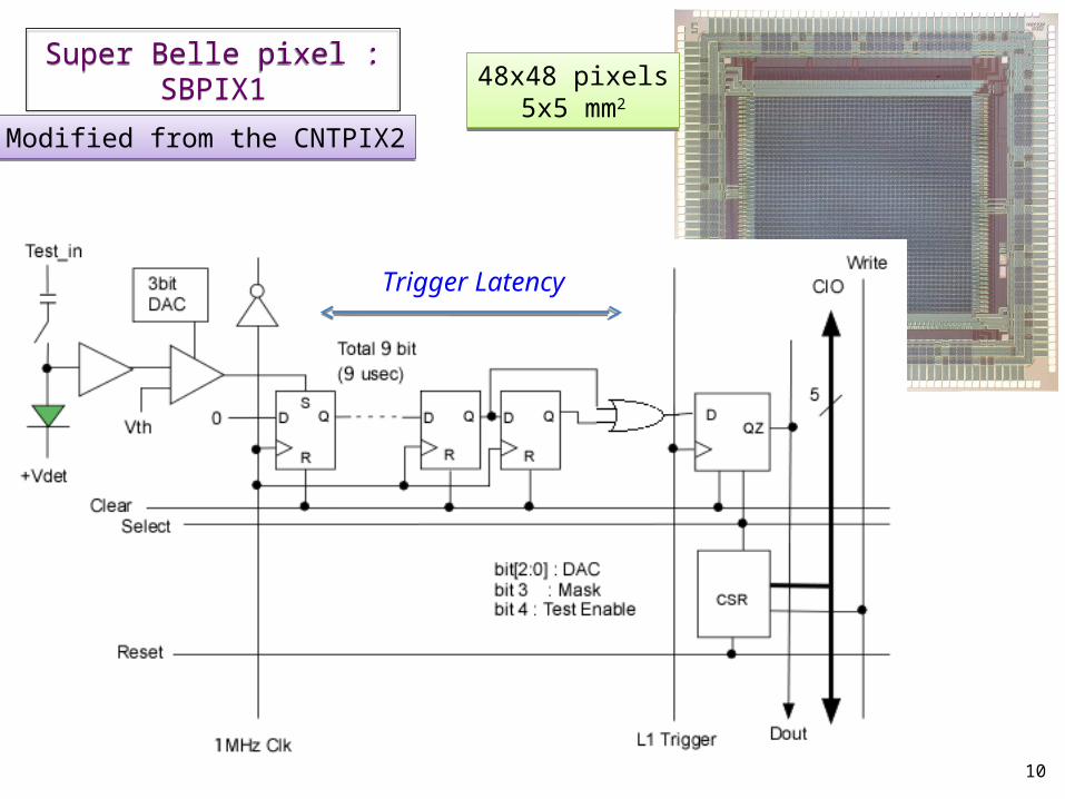
Super Belle pixel : SBPIX1Super Belle pixel : SBPIX1
Trigger Latency
48x48 pixels5x5 mm2
48x48 pixels5x5 mm2
Modified from the CNTPIX2Modified from the CNTPIX2
11
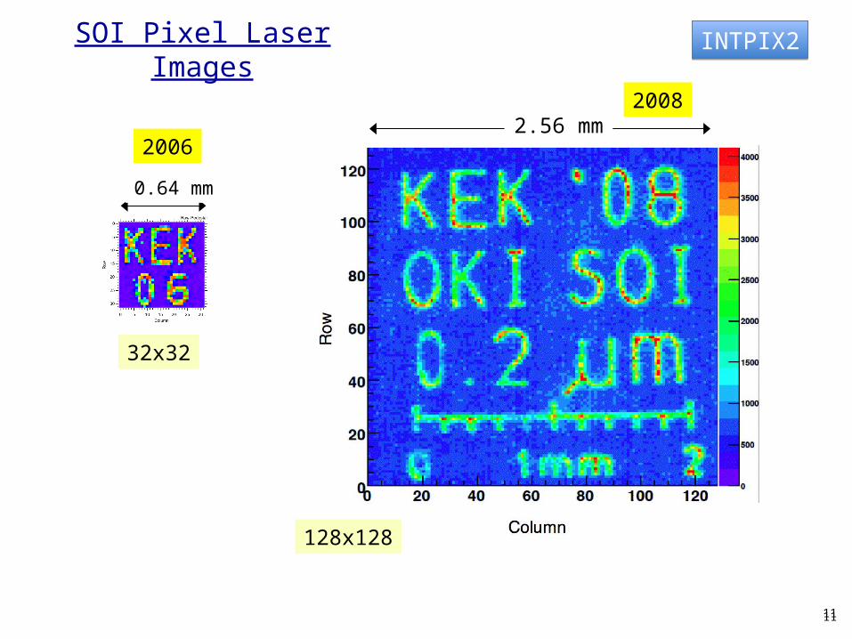
SOI Pixel Laser Images
0.64 mm
2006
32x32
20082.56 mm
128x128
INTPIX2INTPIX2
11
12
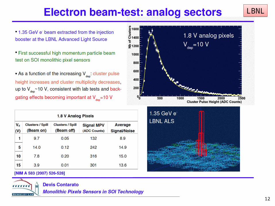
LBNLLBNL
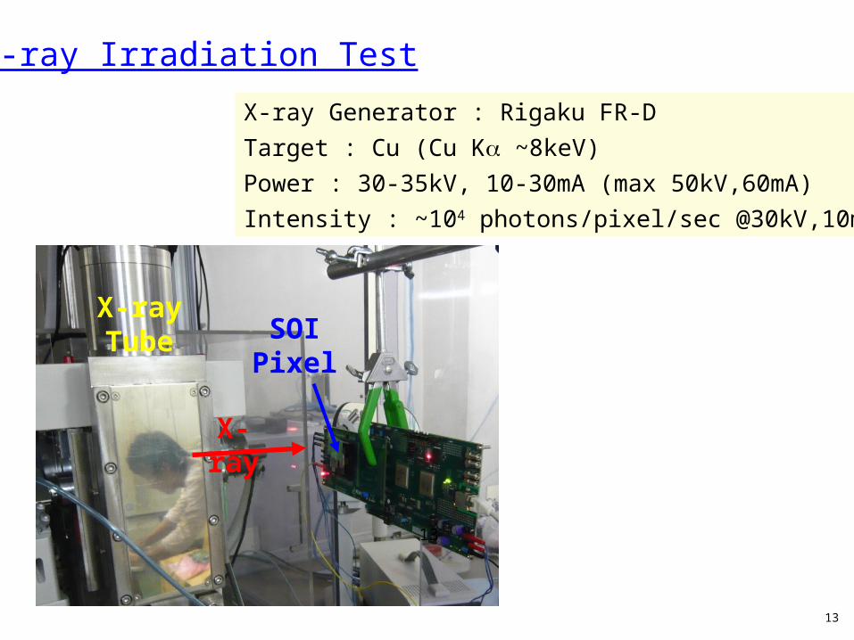
X-ray Irradiation Test
X-ray Tube
X-ray
SOIPixel
X-ray Generator : Rigaku FR-D
Target : Cu (Cu K ~8keV)
Power : 30-35kV, 10-30mA (max 50kV,60mA)
Intensity : ~104 photons/pixel/sec @30kV,10mA
13
13

X-ray Test Chart14
Position resolution(pixel size=20m x 20m)
12.5 16 20 [lp/mm]
INTPIX2INTPIX2
slit w=25m
25 m Slit is well separated.25 m Slit is well separated.14
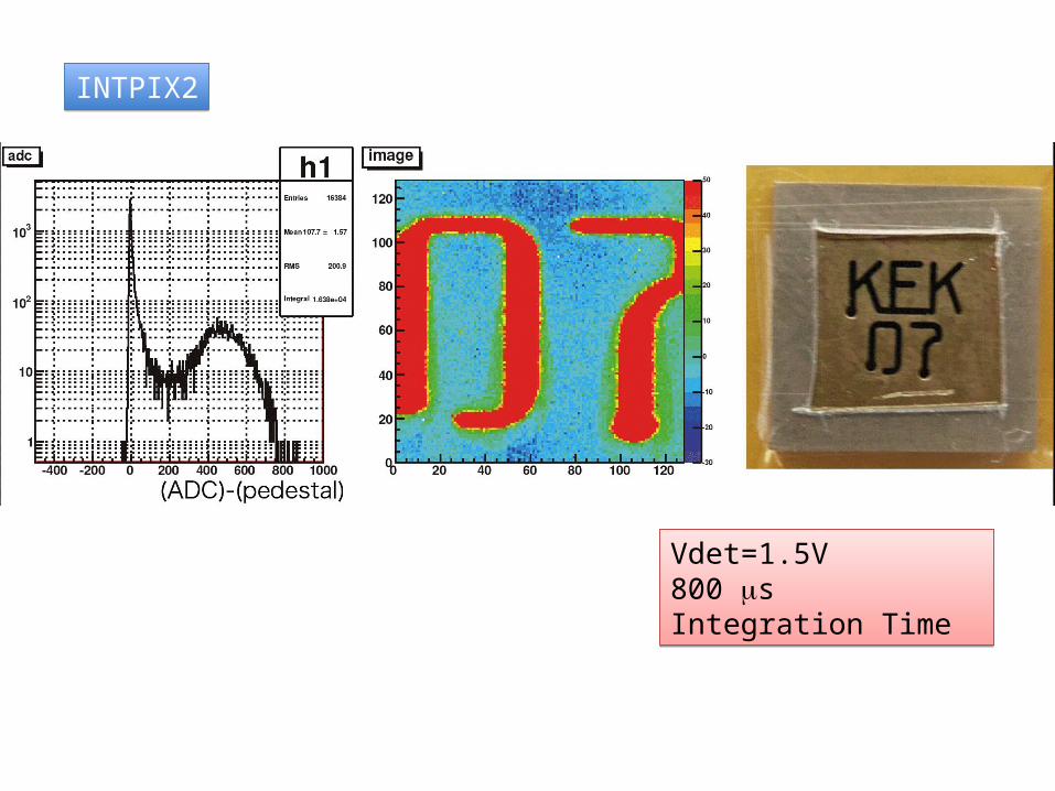
INTPIX2INTPIX2
Vdet=1.5V800 s Integration TimeVdet=1.5V800 s Integration Time
16
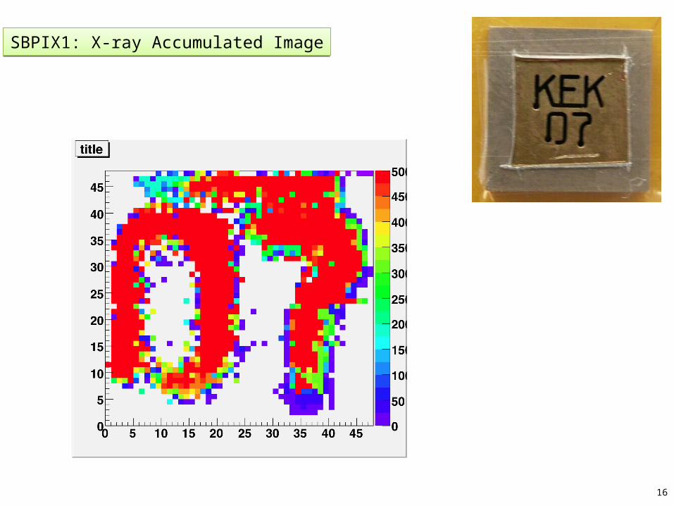
SBPIX1: X-ray Accumulated ImageSBPIX1: X-ray Accumulated Image
5 6.3 8 10 12.5 16 20
[lp/mm]
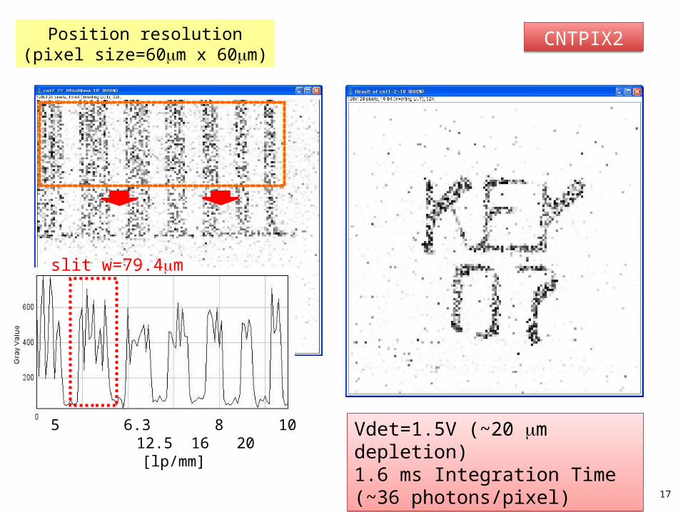
CNTPIX2CNTPIX2Position resolution(pixel size=60m x 60m)
slit w=79.4m
Vdet=1.5V (~20 m depletion)1.6 ms Integration Time(~36 photons/pixel)
Vdet=1.5V (~20 m depletion)1.6 ms Integration Time(~36 photons/pixel)
17

SEABAS test board
INTPIX2 + Lens
Ethernet
18
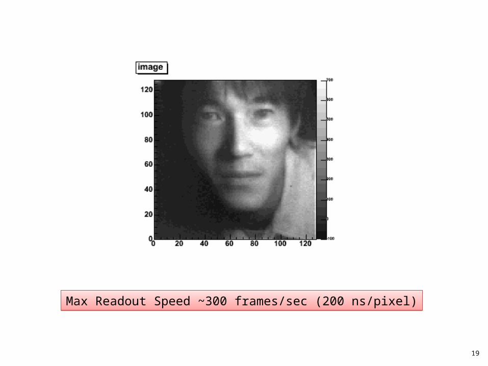
Max Readout Speed ~300 frames/sec (200 ns/pixel)Max Readout Speed ~300 frames/sec (200 ns/pixel)
19

R&D Plans
20
Continue MPW runs : Number of the run will be increased twice/year.FY08 Submission : Feb. 2009FY09 Submission : June and December 2009
Continue MPW runs : Number of the run will be increased twice/year.FY08 Submission : Feb. 2009FY09 Submission : June and December 2009
•Wafer Improvement : Double SOI wafer
•Process Improvement : Implant through SOI layer
•Implementation Improvement : 3D Integration
•Wafer Improvement : Double SOI wafer
•Process Improvement : Implant through SOI layer
•Implementation Improvement : 3D Integration
+
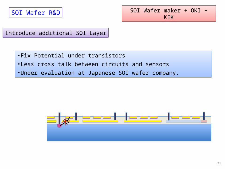
SOI Wafer R&D
•Fix Potential under transistors
•Less cross talk between circuits and sensors
•Under evaluation at Japanese SOI wafer company.
•Fix Potential under transistors
•Less cross talk between circuits and sensors
•Under evaluation at Japanese SOI wafer company.
SOI Wafer maker + OKI + KEKSOI Wafer maker + OKI + KEK
Introduce additional SOI LayerIntroduce additional SOI Layer
21
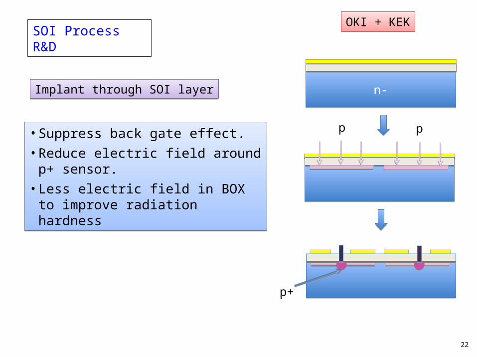
SOI Process R&D
n-n-
p
p+
p• Suppress back gate effect.
• Reduce electric field around p+ sensor.
• Less electric field in BOX to improve radiation hardness
• Suppress back gate effect.
• Reduce electric field around p+ sensor.
• Less electric field in BOX to improve radiation hardness
Implant through SOI layerImplant through SOI layer
OKI + KEKOKI + KEK
22
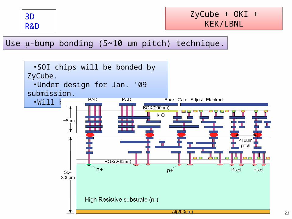
•SOI chips will be bonded by ZyCube.•Under design for Jan. '09 submission.•Will be bonded in Apr. '09.
•SOI chips will be bonded by ZyCube.•Under design for Jan. '09 submission.•Will be bonded in Apr. '09.
ZyCube + OKI + KEK/LBNLZyCube + OKI + KEK/LBNL3D R&D
Use -bump bonding (5~10 um pitch) technique.Use -bump bonding (5~10 um pitch) technique.
23
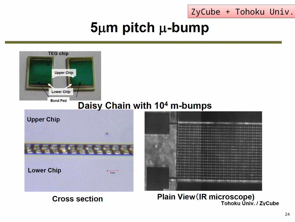
ZyCube + Tohoku Univ.ZyCube + Tohoku Univ.
24
Summary
• The SOI pixel has many good features (monolithic, low material, high speed ...) and a promising candidate for the future Super Belle pixel detector.
• Preliminary test chips are showing good response to light, -rays, X-rays and charged particles.
• The number of the SOI MPW runs will be increased twice per year in 2009.
• We are doing several R&D ('Double SOI wafer', 'through SOI Implant', and '3D Integration' etc.) to get better performance in the SOI Pixel.
• There are still many items not to be tested. We welcome any people who have interests on the SOI pixel.
25


