
Spectromicroscopy for Addressing theSurface and Electron TransportProperties of Individual 1-DNanostructures and Their NetworksAndrei Kolmakov,†,* Sai Potluri,† Alexei Barinov,‡ Tevfik O. Mentes,‡ Luca Gregoratti,‡ Miguel A. Nino,‡
Andrea Locatelli,‡ and Maya Kiskinova‡
†Southern Illinois University at Carbondale, Carbondale, Illinois 62901-4401, and ‡Sincrotrone Trieste, 34012 Basovizza-Trieste, Italy
Implementation of “bottom-up” para-digm in technology is based on fabrica-tion and assembly of artificial objects
with dimensions ranging from a few to a
few hundred nanometers with predesigned
functionalities. Semiconducting quasi-one-
dimensional (quasi-1D) nanostructures, in
particular metal oxide (MOx) nanowires and
nanobelts, are among the most promising
platforms for gas sensing, energy harvest-
ing/conversion, and opto-electronic
applications.1�3 When the effective diam-
eter of these objects shrinks to the nano-
scale, the surface starts to play a significant
role and can even dominate their proper-
ties. For example, the attractive novel prop-
erties of semiconducting metal oxide
nanowires in gas sensing4�8 and electroni-
cally tunable reactivity9,10 have been attrib-
uted to the intimate coupling between sur-
face redox processes and electron
concentration inside the nanostructure. In
order to control this surface ↔ electron
transport interplay and to develop a repro-
ducible nanodevice, the fundamental rela-
tions between the surface composition,
morphology, and electronic structure of ox-
ide nanostructures along with their physi-
cal and chemical properties have to be
identified. The complexity and challenges
in such studies are dictated by two major
factors: (i) the purity (both surface and bulk)
and (ii) the strong size and morphology de-
pendence of the observed phenomena. In
addition, the substrate and electrodes in the
real world devices can induce significant
changes to the electronic properties of the
nanostructure. Therefore, it is desirable to
measure individual and prewired nano-
structures since the results obtained on en-
sembles (bundles, films, etc.) lack size andmorphology specificity.
Up to date, the structural and composi-tional ex situ and in situ characterization ofthe oxide nanostructures has exclusivelybeen performed by means of scanning elec-tron microscopy (SEM) or transmission elec-tron microscopy (TEM).11,12 The imagingand analytical capabilities, combined withthe latest developments of sample stages inthese machines, have allowed in situ explo-ration of the mechanical, compositional,electrical, and other properties of the nano-structures, as well as high-resolution imag-ing and analysis at elevated pressures andtemperatures. Both techniques provide veryhigh spatial resolution, but their spectro-scopic abilities, based on energy-filteredelectron and photon emission, such as elec-tron energy loss, auger electron, and en-ergy dispersive X-ray spectroscopy, are lim-ited in energy resolution and/or surfacesensitivity.
Alternative spectromicroscopy methodswith surface sensitivity are those using X-raysources and detecting photoelectrons
*Address correspondence [email protected].
Received for review May 31, 2008and accepted September 11, 2008.
Published online September 26,2008.10.1021/nn8003313 CCC: $40.75
© 2008 American Chemical Society
ABSTRACT Understanding size/dimensionality-dependent phenomena and processes relevant to chemical
sensing and catalysis requires analytical methods with high surface sensitivity, which can exploit the structure
and composition of nanomaterials at their natural length scales and working conditions. In the present study, we
explored the potentials and complementary capabilities of several surface-sensitive microscopy approaches to
shed light on the properties of individual SnO2 nanowires and their networks. Our results demonstrate the unique
opportunities provided by synchrotron-based photoelectron microscopies for surface-sensitive structural and
chemical analysis, including in situ characterization of electron transport properties of a nanostructure wired as
an active element in chemiresistor devices.
KEYWORDS: SnO2 nanowires · nanobelts · surface · electronspectroscopy · microscopy · PEEM · LEEM · SPEM · LEED · gas sensors · catalysis
ARTIC
LE
www.acsnano.org VOL. 2 ▪ NO. 10 ▪ 1993–2000 ▪ 2008 1993

emitted from the top few layers of the specimen. Inthese X-ray photoelectron microscopies, informationfor the chemical state and electronic structure of thesurface is provided by the two well-developed spectro-scopic methods: (i) X-ray photoelectron spectroscopy(XPS), which uses monochromatic photons to obtainenergy distribution curves of the photoelectrons emit-ted from discrete atomic electron levels,13 and (ii) X-rayabsorption near-edge spectroscopy (XANES), wherethe total electron yield spectra are measured while vary-ing the photon energy around the X-ray absorptionthresholds corresponding to a given core electron bind-ing energy.14 Along with the surface chemical sensitiv-ity, another advantage of these photoelectron-basedspectroscopies is that the radiation damage, which caninduce irreversible structural and chemical changes inthe nano-object, is weaker using X-rays relative to theelectron beam. Probing the matter at submicrometerlength scales using XPS and/or XANES requires the in-tense and tunable X-rays provided at the third genera-tion synchrotron facilities. The spatial resolution isachieved using two different approaches, which clas-sify the microscopies as scanning and full-fieldimaging.15�17 In the scanning photoelectron micros-copy (SPEM), the incident photon beam is demagnifiedto a submicrometer (ca. 100�200 nm) spot onto thesample, which can be raster scanned with respect to themicroprobe. In the X-ray photoelectron emissionmicroscopies (XPEEM), a magnified image of the irradi-ated area is obtained by projection of the emitted elec-trons using appropriate electron tailoring optics. Thesesynchrotron-based microscopies can be successfullycomplemented with conventional surface sciencemethods for structural analysis, as low energy electrondiffraction (LEED) and low energy electron microscopy
(LEEM). In fact, an important advantage of XPEEM in-struments is the possibility to perform LEEM in the samesetup,18 which provide complementary morphologicalinformation with spatial resolution of 10 nm and mi-crospot LEED monitoring the long-range atomic orderfrom an area of 1�2 �m. SPEM and XPEEM have suc-cessfully been used for analysis of C and MoSx
nanotubes,19�25 GaN nanowire,26 oxide nanoparticles,and wires.27,28 A few experimental impediments forPEEM imaging and spectroscopy on an individualprewired nanowire chemiresistor were reported in ourprevious work,29 and some solutions were proposed.
This communication reports on the surface struc-ture, composition, and morphology of individualquasi-1D SnO2 nanostructures, their percolating net-works, and corresponding transport properties whenthey are indexed as a part of the device. The results, ob-tained by combining surface-sensitive spectromicros-copy and transport measurement methods, providenew important information for these nanomaterials.The surface and sensor properties of the macroscopiccounterparts selected for this study of SnO2 nanostruc-tures are already well-known,30 and we have developedfabrication and handling protocols, which preservetheir surface cleanliness (see ref 31 and supporting ma-terial therein).
RESULTS AND DISCUSSIONThe SPEM and X-PEEM/LEEM experiments were per-
formed at the ESCAmicroscopy32 and Nanospectros-copy beamlines17 at ELETTRA synchrotron radiation fa-cility, hosting the SPEM and XPEEM-LEEM instruments,respectively. The XPEEM-LEEM is equipped with a hemi-spherical electron analyzer, reaching an energy resolu-tion of 200 meV, and provides the complementary spec-
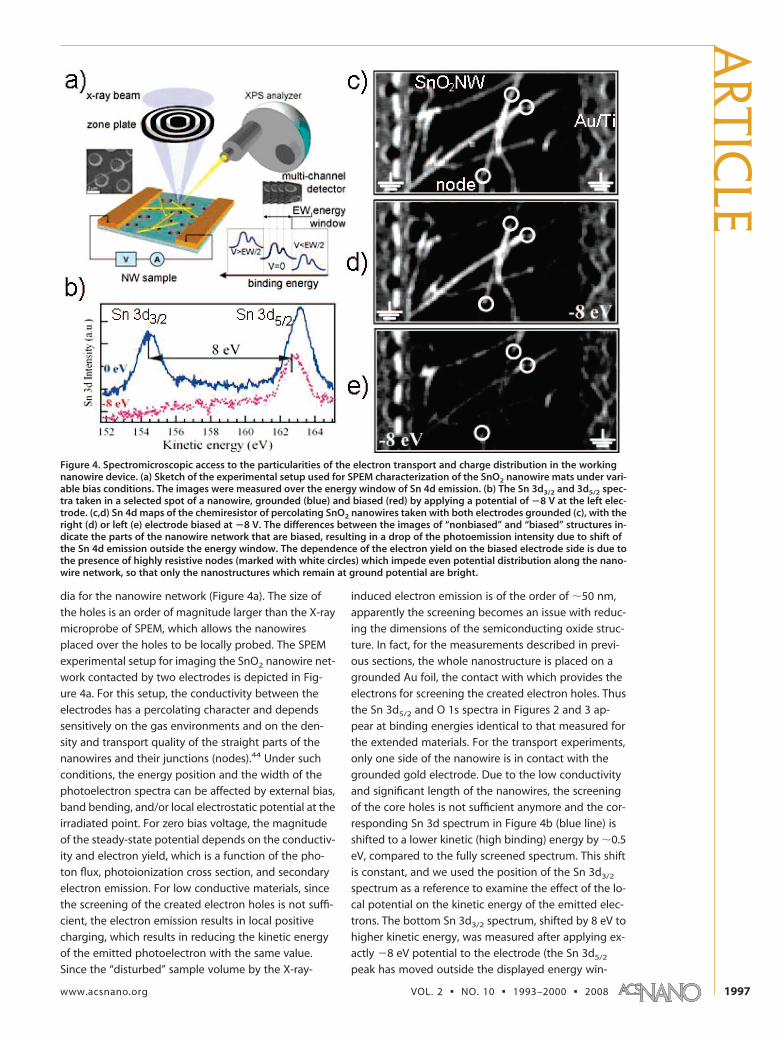
Figure 1. (a,b) Two LEEM images (FOV 20 �m) and (c,d) corresponding (1 � 1) LEED patterns collected from the two areas(marked with white circles) along the individual nanostructure. The rotation of the (1 � 1) LEED patterns approximately fol-lows the bending of the nanostructure in real space. (e) LEEM (FOV 6 �m, 5.5 eV) image of the “kinked” nanostructure and(1 � 1) LEED patterns (45 eV) collected from different “arms”. In spite of the changed orientation in the real space, the sur-face structure and its orientation are preserved along the length of the nanostructure. The inset depicts the model of the(010) facet and crystallographically equivalent growth directions.
ART
ICLE
VOL. 2 ▪ NO. 10 ▪ KOLMAKOV ET AL. www.acsnano.org1994

troscopic methods XANES and XPS. The lateralresolution is 10 nm in LEEM operation mode and a fewtens of nanometers in energy-filtered X-PEEM imaging.The instrument can also perform micro-LEED andmicro-XPS measurements, restricted to an area of 2�m in diameter.
Surface Structure of the Individual Nanostructure. Figure1a,b depicts LEEM images of two different parts of thesame SnO2 nanowire (here we are using the generalterm “nanowire” since the resolution is not sufficientto distinguish between nanostructures with differentmorphologies). Panels c and d represent the micro-LEED patterns collected at two locations (marked withwhite circles in a and b). Moving the sample in front ofthe LEEM objective, we were able to monitor the evolu-tion of LEED patterns along the nanostructure’s length.Both 1 � 1 micro-LEED patterns, marked by the whitedashed line, correspond to a rutile surface unit cell withreal space dimensions, (3.23 � 0.1 Å) � (4.88 � 0.12Å), in agreement with the ones from (010) or (100) fac-ets of the SnO2 rutile crystals.33 Soley on the basis of theLEED pattern, it is not possible to discriminate be-tween these two facets. However, on the basis of previ-ous HRTEM results showing that the preferable growthdirection is [101] and (101)/(010) top/side faceting ofSnO2 rutile nanobelts and nanowires with rectangularcross section,34 most probably the LEED pattern corre-sponds to a (010) side facet of the nanowire. This assign-ment is supported by the facile bending of the nano-wire/nanobelt in this plane and the appearance ofweaker diffraction spots in the LEED pattern. The latterones are evidence of the single twin structure in thenanowire/nanobelt. Very similar SAED patterns, takenalong the [010] zone axis, have been previously re-ported34 for large diameter nanobelts, which agreewell with our assignment.
Another class of quasi-1D nanostructures, exploredby LEED, is nanowires which change their growth direc-tion due to perturbed growth conditions while preserv-ing their crystallographic orientation. In contrast to thenanobelt case, the V-shaped (“kinked”) nanostructure inFigure 1e shows the same LEED pattern independentlyof the position. This observation corroborates nicelywith previous HRTEM studies of the segmented and zig-zag SnO2 nanostructures, which have shown that suchstructures are in fact “sculptured” single crystals andtheir growth axis can be altered into crystallographi-cally equivalent directions by tiny changes in thegrowth conditions.35,36 Again, the LEED pattern in Fig-ure 1e corresponds to the (010) facet of the nanostruc-ture. Assuming that the growth takes place along the[101] and [101] directions, the angle at the kink is ex-pected to be 67.9°, in agreement with the experimen-tally determined value of �70°.
XANES and XPS on Individual Nanostructures. Figure 2shows the XANES spectrum (green top line) of the SnO2
nanobelt, measured with X-PEEM by collecting stacks
of images while scanning the photon energy aroundthe Sn 3d edge. For comparison, the XANES spectra ofrutile SnO2 (red) and tetragonal SnO (blue) samples, re-ported in ref 37, are also shown. Analogous to themacroscopic counterparts, the XANES spectrum fromthe individual nanostructure consists of the Sn 3d5/2
and 3d3/2 features (separated by �8.5 eV), giving riseto six major transitions into the unoccupied Sn elec-tronic states. Close inspection of the three spectra inFigure 2 reveals that in spite of the general similaritythere are some differences in the relative intensity andshape of the nanobelt peaks, most evident in the 3�4eV range. The enhanced relative intensity of the 4.2 eVpeak, reported previously in ref 37, has been attributedto oxygen deficiency, induced by surface reconstruc-tion. Since our LEED patterns do not evidence a recon-struction, this suggests that the nanobelt surface is par-tially reduced and the spectrum contains overlappingfeatures of the SnO2 and SnO phases, as indicated in thefigure.
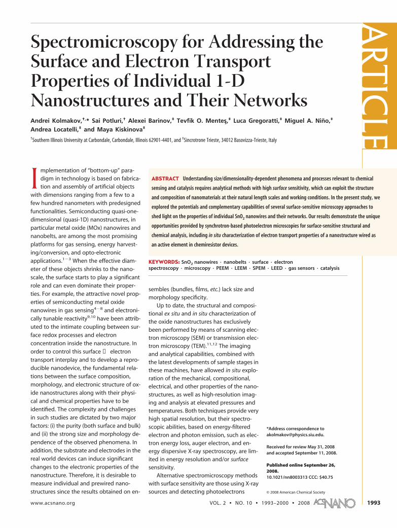
More detailed information for the surface chemicalstate has been obtained from the photoelectron spec-tra of individual SnO2 nano(meso)structures, measuredby SPEM, where the incident photon beam is focused toa small spot (100�200 nm). SPEM can be operated intwo modes: (i) imaging by collecting photoelectronswithin a selected kinetic energy window (Figure 3a),while scanning the sample with respect to the focusedbeam, and (ii) conventional energy dispersive electronspectroscopy from the illuminated local spot (micro-XPS) (Figure 3b�d). When the element under consider-ation is present in a single chemical state, the spatialvariation in the contrast of the images reflects the varia-tion of the photoelectron yield, which is a measure ofthe local concentration of the element. Figure 3a showsthe Sn 4d image of a SnO2 nanobelt (bright) placed on
Figure 2. XANES spectrum (green) taken at room temperatureon an individual SnO2 nanowire obtained as a ratio of the grayscale signals form XPEEM (inset) images of the nanowire andbackground while scanning the photon energy from 480 to 505eV. For comparison, XAS spectra from bulk SnO (blue) and SnO2
(red) (adapted from ref 36) are shown. The energy scale is off-set with respect to the first maximum of Sn 3d5/2.
ARTIC
LE
www.acsnano.org VOL. 2 ▪ NO. 10 ▪ 1993–2000 ▪ 2008 1995
a gold support (dark). Figure 3b shows two representa-
tive sets of O 1s, Sn 3d5/2, and VB spectra measured on
microspots of a freshly oxygen-plasma-treated nano-
structure (bottom spectra) and after annealing to 523
K in UHV (top spectra). The spectra are deconvoluted
considering the reported binding energy of Sn 3d5/2
and O 1s core levels of SnO and SnO2 macroscopic poly-
crystalline and single-crystal samples.38�41 The pres-
ence of SnO-derived components in the O 1s and Sn
3d5/2 spectra is in accordance with the XANES spectra
in Figure 2. This should be attributed to lattice oxygen
deficiency and reduced oxygen concentration at the
surface, becoming more prominent after annealing to
523 K. The spectra from the fresh oxygen-plasma-
treated sample have a weaker SnO component and
contain also a third high BE component, which domi-
nates the O 1s spectra. According to the literature,41 the
rather broad component at �531.7 eV (marked with
yellow in Figure 3b) apparently originates from chemi-
sorbed O-containing species, such as O��, O2��, or
OH��. Correspondingly, the high BE component in the
Sn 3d5/2 spectra can tentatively be attributed to surface
Sn atoms bound to adsorbed species, resulting in O co-
ordination higher than that in SnO2. The relatively high
intensity of the “Ochem” component is due to the very
high surface sensitivity, resulting from the low kinetic
energy of the O 1s and Sn 3d5/2 photoelectrons and the
grazing acceptance geometry of the energy analyzer
in SPEM. The origin of this component is confirmed by
its strong attenuation due to desorption upon anneal-
ing to 523 K. The Ochem component also gradually loses
intensity under prolonged X-ray irradiation at room
temperature due to photon-induced desorption,
whereas the oxide components remain practically in-
tact. The VB spectra in Figure 3d are measured with a
lower surface sensitivity due to the high photoelectron
kinetic energy. They are dominated by the SnO2 main
peaks centered at �5, 8, and 11 eV, originating from
the O(2p) nonbonding, Sn(5s)�O(2p), and
Sn(5p)�O(2p) states, respectively, whereas the SnO-
related features at �3, 6.5, and 9.7 eV are appearing as
weak shoulders.42 The only distinct difference in the VB
spectra of a fresh and annealed nanostructure is the in-
crease of the emission at �3 eV, attributed to
Sn(5s�5p)-hybridized states in the SnO band gap.37,41
It is clearly manifested by the VB spectral difference
shown by the dashed line in panel d. These results sup-
port that the oxygen deficiency is mostly at the sur-
face and, due to the larger probing depth, is not very
evident in the VB spectra.
Addressing the Electron Transport in a Working Device. When
the SnO2 nanostructures are wired as active elements
in nanodevices, their electronic and surface properties
cannot be fully decoupled from effects induced by
other parts of the nanodevice such as electrodes, sup-
port, etc. Some examples of possible effects on the
nanowire properties are the electrostatically controlled
reactivity,43 the gate-induced electrodesorption,10 and
the influence of the mobile parasitic charges on the
transport properties.44 In order to get insight into how
these phenomena affect the electronic status of the
nanostructures, wired as part of a device, the analytical
measurements have to be performed under conditions
close or identical to the working ones. The straightfor-
ward application of the photoelectron spectromicros-
copy to working nanodevices is generally hampered by
parasitic charging since the standard device architec-
tures routinely involve isolating layers or support in the
proximity of the nanostructure.45 One of the possible
solutions is to use a model UHV-compatible device con-
taining a suspended nanostructure similar to the one
described in ref 29. For the present study, we fabricated
a model chemiresistor gas sensing device using Si3N4
membranes with periodic 2 �m holes as a support me-
Figure 3. (a) Large- and small-scale chemical image of an individual SnO2 nanobelt obtained by monitoring the Sn 4d photoelectrons.(b) O 1s, (c) Sn 3d5/2, and (d) VB spectra taken from the SnO2 nanobelt after oxygen plasma treatment (bottom spectrum in each panel,measured at room temperature) and after annealing at 523 K (top spectrum in each panel, measured at 523 K). The SnO band gap peak re-sulting from subtraction of the bottom from the top VB spectrum is shown by the dashed line in panel d.
ART
ICLE
VOL. 2 ▪ NO. 10 ▪ KOLMAKOV ET AL. www.acsnano.org1996
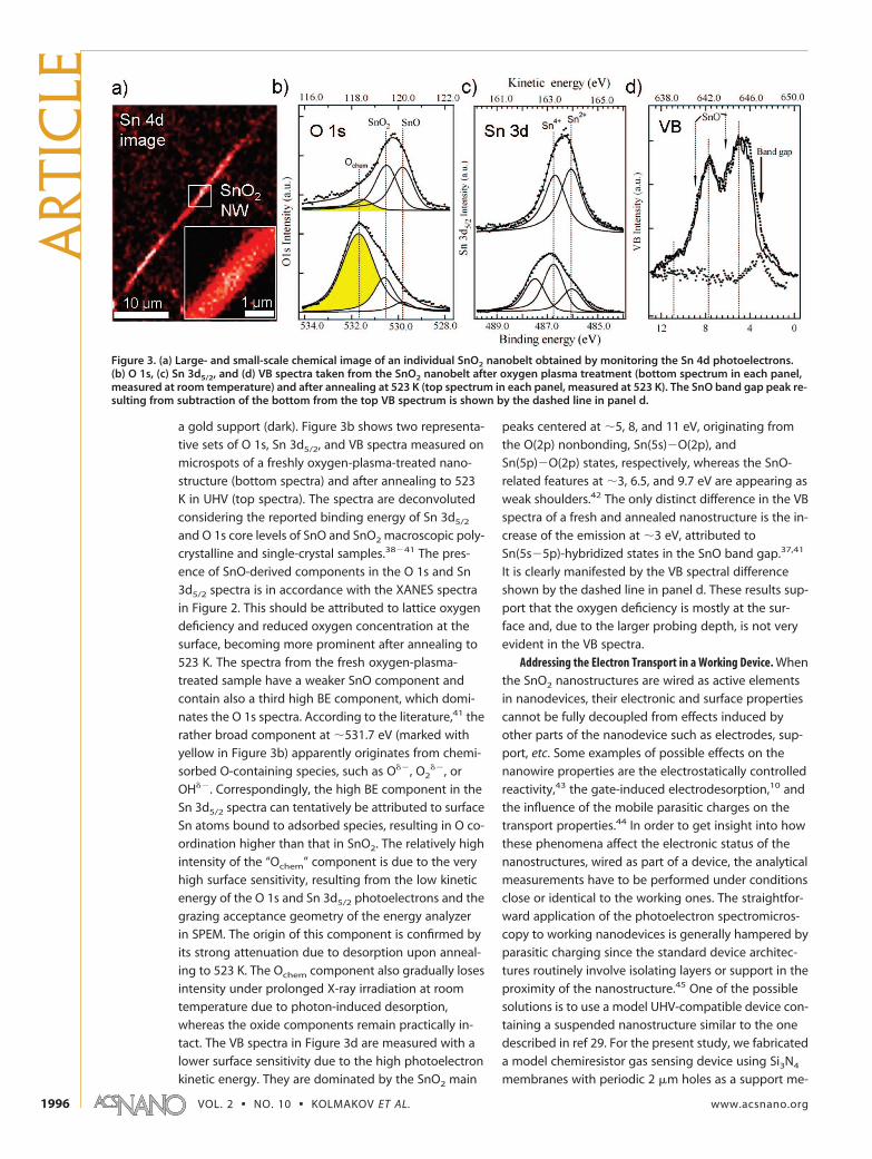
dia for the nanowire network (Figure 4a). The size of
the holes is an order of magnitude larger than the X-ray
microprobe of SPEM, which allows the nanowires
placed over the holes to be locally probed. The SPEM
experimental setup for imaging the SnO2 nanowire net-
work contacted by two electrodes is depicted in Fig-
ure 4a. For this setup, the conductivity between the
electrodes has a percolating character and depends
sensitively on the gas environments and on the den-
sity and transport quality of the straight parts of the
nanowires and their junctions (nodes).44 Under such
conditions, the energy position and the width of the
photoelectron spectra can be affected by external bias,
band bending, and/or local electrostatic potential at the
irradiated point. For zero bias voltage, the magnitude
of the steady-state potential depends on the conductiv-
ity and electron yield, which is a function of the pho-
ton flux, photoionization cross section, and secondary
electron emission. For low conductive materials, since
the screening of the created electron holes is not suffi-
cient, the electron emission results in local positive
charging, which results in reducing the kinetic energy
of the emitted photoelectron with the same value.
Since the “disturbed” sample volume by the X-ray-
induced electron emission is of the order of �50 nm,
apparently the screening becomes an issue with reduc-
ing the dimensions of the semiconducting oxide struc-
ture. In fact, for the measurements described in previ-
ous sections, the whole nanostructure is placed on a
grounded Au foil, the contact with which provides the
electrons for screening the created electron holes. Thus
the Sn 3d5/2 and O 1s spectra in Figures 2 and 3 ap-
pear at binding energies identical to that measured for
the extended materials. For the transport experiments,
only one side of the nanowire is in contact with the
grounded gold electrode. Due to the low conductivity
and significant length of the nanowires, the screening
of the core holes is not sufficient anymore and the cor-
responding Sn 3d spectrum in Figure 4b (blue line) is
shifted to a lower kinetic (high binding) energy by �0.5
eV, compared to the fully screened spectrum. This shift
is constant, and we used the position of the Sn 3d3/2
spectrum as a reference to examine the effect of the lo-
cal potential on the kinetic energy of the emitted elec-
trons. The bottom Sn 3d3/2 spectrum, shifted by 8 eV to
higher kinetic energy, was measured after applying ex-
actly �8 eV potential to the electrode (the Sn 3d5/2
peak has moved outside the displayed energy win-
Figure 4. Spectromicroscopic access to the particularities of the electron transport and charge distribution in the workingnanowire device. (a) Sketch of the experimental setup used for SPEM characterization of the SnO2 nanowire mats under vari-able bias conditions. The images were measured over the energy window of Sn 4d emission. (b) The Sn 3d3/2 and 3d5/2 spec-tra taken in a selected spot of a nanowire, grounded (blue) and biased (red) by applying a potential of �8 V at the left elec-trode. (c,d) Sn 4d maps of the chemiresistor of percolating SnO2 nanowires taken with both electrodes grounded (c), with theright (d) or left (e) electrode biased at �8 V. The differences between the images of “nonbiased” and “biased” structures in-dicate the parts of the nanowire network that are biased, resulting in a drop of the photoemission intensity due to shift ofthe Sn 4d emission outside the energy window. The dependence of the electron yield on the biased electrode side is due tothe presence of highly resistive nodes (marked with white circles) which impede even potential distribution along the nano-wire network, so that only the nanostructures which remain at ground potential are bright.
ARTIC
LE
www.acsnano.org VOL. 2 ▪ NO. 10 ▪ 1993–2000 ▪ 2008 1997

dow). Since all emitted photoelectrons undergo thesame potential-induced kinetic energy shift, the posi-tion (and presence) of core level peak (i.e., Sn 3d, 4dused in this study) in the energy window of the ana-lyzer depends on local electrostatic potential of theprobed area. The potential of SPEM for analyzing thecharge distribution and transport properties of work-ing nanodevices, based on the demonstrated correla-tion between the applied potential and kinetic energyof the emitted photoelectrons is best illustrated by theSPEM images in Figure 4c�e. They show a percolatingnanowire network measured under three different bias-ing conditions. The energy window of 7.8 eV was tunedaround the Sn 4d emission of nonbiased nanowires,which appear as bright stripes in Figure 4c. On the leftand right side of the image, the metal electrodes arealso distinct due to the intense secondary electronemission. The biasing of the right or left electrode (Fig-ure 4d,e) results in very strong attenuation of the pho-toelectron signal (due to energy shift beyond the Sn 4denergy window) only from certain SnO2 wires, whichdepends on the biased electrode. By close inspectionof the images in Figure 4c,d, one can identify somewires with rather good conductivity, which remain vis-ible and confined points (nods) of the high resistivitywhere nearly all potential drops and the entire groupof nanowires disappear from the image up to the junc-tion point. As can be expected by biasing (Figure 4e) ofthe opposite electrode, a complementing part of thenetwork becomes visible again up to the same junc-tion points.
SUMMARYUsing several powerful spectromicroscopy and
microscopy surface science tools, namely, X-PEEM,
SPEM, LEEM, and LEED, we obtained new information
about the composition and structure of individual
metal oxide nanowires and their 2D networks. The
micro-LEED patterns obtained for the first time on indi-
vidual SnO2 nanowires confirm the (010) structure of
the side facets and the preservation of the single-crystal
orientation of the “kinked” nanostructures. Micro-XPS
and XANES measured from the individual nanowires
and nanobelts reveal surface stoichiometry, coordina-
tion, and oxidation state of the nanostructures similar to
their macroscopic counterparts. Being extremely impor-
tant for electronic screening effects, apparently 100
nm size domain is still too large to induce measurable
size effects. The potential of SPEM to explore electron
transport in the working chemiresistor device com-
posed of mats of the percolating nanowires has al-
lowed us to identify the presence of “electroactive” ele-
ments which control the transport through the entire
percolating nanowire network. This approach opens
new avenues to explore the surface structural and elec-
tronic properties of individual nanostructures as a func-
tion of nanostructure size, morphology, type of adsor-
bate, and temperature. In addition, we have shown that
the method is applicable to the nanostructures wired
as an active element of the functioning nanodevice
(chemiresistor in our case). The latter offers a unique ex-
perimental platform for in situ and in real time studies
in order to link fundamental surface processes taking
place on the nanowire surface with the corresponding
electronic and transport properties.
METHODSPristine single-crystal quasi-1D SnO2 nanowires and nano-
belts were synthesized from SnO at ca. 1220 K in Ar flux (35sccm) using the vapor�solid (VS) growth protocol. As-preparednanostructures, with diameters and lengths in the range of100�500 nm and 10�300 �m, correspondingly, were trans-ferred from the alumina crucible and dry deposited on (i) a cleanSi (111) wafer with native oxide layer for X-PEEM/LEEM measure-ments and (ii) a Au foil for SPEM characterization. A model nan-odevice, which allows in situ SPEM characterization under biasingconditions, was prepared placing the 2D network of cross-linkedSnO2 nanowires on a perforated Si3N4 membrane (with peri-odic 2 �m holes (Aquamarijn Micro Filtration BV)) and evaporat-ing on top of the nanowire network a few Au/Ti electrodesthrough a shadow mask. The distance between electrodes wasca. 20 �m. The average density of the nanowires in the networkwas r � 0.036 �m�2, which was close to the percolation thresh-old r � 0.04 �m�2. This SnO2 nanowire/Si3N4 unit was placedand wire bonded in a ceramic chip holder. Wet processing (asthose used in resist-based lithography) is avoided because it cancontaminate the surface of the nanostructure and support andaffect chemical and transport properties. The small amount ofweakly bound C-containing species on nanostructure and de-vice surfaces is unavoidable when the materials are in air (seesurvey XPS in ref 31). They are cleaned by brief annealing in
vacuum and by oxygen plasma treatment before SPEM and X-PEEM/LEEM measurements. In particular, the sample was an-nealed at 530 K for a few minutes using indirect electron bom-bardment heating on the back side of the Au support. Theoxygen flux was provided from a TECTRA radio frequency plasmasource providing O flux of the order of 1015 atoms cm�2 min�1.
Acknowledgment. We thank Ulrike Diebold for helpful discus-sions. The technical support of Clay Watts and Joshua Cothren(SIUC) is greatly acknowledged. SIUC part of the research wassupported by through ACS PRF# 45842-G5 grant.
REFERENCES AND NOTES1. Lieber, C. M. Nanoscale Science and Technology: Building
a Big Future From Small Things. MRS Bull. 2003, 28,486–491.
2. Xia, Y. N.; Yang, P. D.; Sun, Y. G.; Wu, Y. Y.; Mayers, B.; Gates,B.; Yin, Y. D.; Kim, F.; Yan, Y. Q. One-DimensionalNanostructures: Synthesis, Characterization, andApplications. Adv. Mater. 2003, 15, 353–389.
3. Wang, Z. L. Functional Oxide Nanobelts: Materials,Properties and Potential Applications in Nanosystems andBiotechnology. Annu. Rev. Phys. Chem. 2004, 55, 159–196.
4. Cui, Y.; Wei, Q. Q.; Park, H. K.; Lieber, C. M. NanowireNanosensors for Highly Sensitive and Selective Detection
ART
ICLE
VOL. 2 ▪ NO. 10 ▪ KOLMAKOV ET AL. www.acsnano.org1998

of Biological and Chemical Species. Science 2001, 293,1289–1292.
5. Law, M.; Kind, H.; Messer, B.; Kim, F.; Yang, P. D.Photochemical Sensing of NO2 with SnO2 NanoribbonNanosensors at Room Temperature. Angew. Chem., Int. Ed.2002, 41, 2405–2408.
6. Comini, E.; Faglia, G.; Sberveglieri, G.; Pan, Z. W.; Wang,Z. L. Stable and Highly Sensitive Gas Sensors Based onSemiconducting Oxide Nanobelts. Appl. Phys. Lett. 2002,81, 1869–1871.
7. Kolmakov, A.; Zhang, Y. X.; Cheng, G. S.; Moskovits, M.Detection of CO and O2 Using Tin Oxide NanowireSensors. Adv. Mater. 2003, 15, 997–1001.
8. Zhang, D. H.; Liu, Z. Q.; Li, C.; Tang, T.; Liu, X. L.; Han, S.; Lei,B.; Zhou, C. W. Detection of NO2 Down to ppb LevelsUsing Individual and Multiple In2O3 Nanowire Devices.Nano Lett. 2004, 4, 1919–1924.
9. Zhang, Y.; Kolmakov, A.; Lilach, Y.; Moskovits, M. ElectronicControl of Chemistry and Catalysis at the Surface of anIndividual Tin Oxide Nanowire. J. Phys. Chem. B 2005, 109,1923–1929.
10. Fan, Z. Y.; Lu, J. G. Gate-Refreshable Nanowire ChemicalSensors. Appl. Phys. Lett. 2005, 86, 123510–123513.
11. Wang, Z. L. New Developments in Transmission ElectronMicroscopy for Nanotechnology. Adv. Mater. 2003, 15,1497–1514.
12. Bell, D. C.; Wu, Y.; Barrelet, C. J.; Gradecak, S.; Xiang, J.;Timko, B. P.; Lieber, C. M. Imaging and Analysis ofNanowires. Microsc. Res. Tech. 2004, 64, 373–389.
13. Siegbahn, K. From X-ray to Electron-Spectroscopy andNew Trends. J. Electron Spectrosc. Relat. Phenom. 1990, 51,11–36.
14. Stohr, J. NEXAFS Spectroscopy; Springer Series in SurfaceSciences 25, Springer Verlag: Berlin, 1992.
15. Gunther, S.; Kaulich, B.; Gregoratti, L.; Kiskinova, M.Photoelectron Microscopy and Applications in Surface andMaterials Science. Prog. Surf. Sci. 2002, 70, 187–260.
16. Frazer, B. H.; Girasole, M.; Wiese, L. M.; Franz, T.; De Stasio,G. Spectromicroscope for the Photoelectron Imaging ofNanostructures with X-rays SPHINX: Performance inBiology, Medicine and Geology. Ultramicroscopy 2004, 99,87–94.
17. Locatelli, A.; Aballe, L.; Mentes, T. O.; Kiskinova, M.; Bauer,E. Photoemission Electron Microscopy with ChemicalSensitivity: SPELEEM Methods and Applications. Surf.Interface Anal. 2006, 38, 1554–1557.
18. Bauer, E. LEEM Basics. Surf. Rev. Lett. 1998, 5, 1275–1286.19. Chiou, J. W.; Yueh, C. L.; Jan, J. C.; Tsai, H. M.; Pong, W. F.;
Hong, I. H.; Klauser, R.; Tsai, M. H.; Chang, Y. K.; Chen, Y.Electronic Structure of the Carbon Nanotube Tips Studiedby X-ray Absorption Spectroscopy and ScanningPhotoelectron Microscopy. Appl. Phys. Lett. 2002, 81,4189–4191.
20. Goldoni, A.; Larciprete, R.; Gregoratti, L.; Kaulich, B.;Kiskinova, M.; Zhang, Y.; Dai, H.; Sangaletti, L.; Parmigiani,F. X-ray Photoelectron Microscopy of the C 1s Core Levelof Free-Standing Single-Wall Carbon Nanotube Bundles.Appl. Phys. Lett. 2002, 80, 2165–2167.
21. Suzuki, S.; Watanabe, Y.; Ogino, T.; Heun, S.; Gregoratti, L.;Barinov, A.; Kaulich, B.; Kiskinova, M.; Zhu, W.; Bower, C.; etal. Extremely Small Diffusion Constant of Cs in MultiwalledCarbon Nanotubes. J. Appl. Phys. 2002, 92, 7527�7531.
22. Suzuki, S.; Watanabe, Y.; Ogino, T.; Heun, S.; Gregoratti, L.;Barinov, A.; Kaulich, B.; Kiskinova, M.; Zhu, W.; Bower, C.; etal. Electronic Structure of Carbon Nanotubes Studied byPhotoelectron Spectromicroscopy. Phys. Rev. B 2002, 66,035414�035418.
23. Hong, I. H.; Chiou, J. W.; Wang, S. C.; Klauser, R.; Pong,W. F.; Chen, L. C.; Chuang, T. J. Electronic Structure ofAligned Carbon Nanotubes Studied by ScanningPhotoelectron Microscopy. J. Phys. IV 2003, 104, 467–470.
24. Suzuki, S.; Watanabe, Y.; Ogino, T.; Homma, Y.; Takagi, D.;Heun, S.; Gregoratti, L.; Barinov, A.; Kiskinova, M.Observation of Single-Walled Carbon Nanotubes byPhotoemission Microscopy. Carbon 2004, 42, 559–563.
25. Kovac, J.; Zalar, A.; Remskar, M.; Mrzel, A.; Mihailovic, D.;Gregoratti, L.; Kiskinova, M. Elettra Highlights.Inww.elettra.trieste.it/science/highlights/index.html, 2003.
26. Chiou, J. W.; Jan, J. C.; Tsai, H. M.; Pong, W. F.; Tsai, M. H.;Hong, I. H.; Klauser, R.; Lee, J. F.; Hsu, C. W.; Lin, H. M.; et al.Electronic Structure of GaN Nanowire Studied by X-ray-Absorption Spectroscopy and Scanning PhotoelectronMicroscopy. Appl. Phys. Lett. 2003, 82, 3949�3951.
27. Nolting, F.; Luning, J.; Rockenberger, J.; Hu, J.; Alivisatos,A. P. A PEEM Study of Small Agglomerates of Colloidal IronOxide Nanocrystals. Surf. Rev. Lett. 2002, 9, 437–440.
28. Xiao, Y.; Cai, Z.; Wang, Z. L.; Lai, B.; Chu, Y. S. An X-rayNanodiffraction Technique for Structural Characterizationof Individual Nanowires. J. Synchrotron Radiat. 2005, 12,124–128.
29. Kolmakov, A.; Lanke, U.; Karam, R.; Shin, J.; Jesse, S.; Kalinin,S. V. Application of Spectromicroscopy Tools to ExploreLocal Origins of Sensor Activity in Quasi-1D OxideNanostructures. Nanotechnology 2006, 17, 4014–4018.
30. Batzill, M.; Diebold, U. The Surface and Materials Science ofTin Oxide. Prog. Surf. Sci. 2005, 79, 47–154.
31. Sysoev, V.; Goschnick, J.; Schneider, T.; Strelcov, E.;Kolmakov, A. A Gradient Microarray Electronic Nose Basedon Percolating SnO2 Nanowire Sensing Elements. NanoLett. 2007, 7, 3182–3188.
32. Gregoratti, L.; Barinov, A.; Benfatto, E.; Cautero, G.; Fava, C.;Lacovig, P.; Lonza, D.; Kiskinova, M.; Tommasini, R.; Mahl,S.; et al. 48-Channel Electron Detector for PhotoemissionSpectroscopy and Microscopy. Rev. Sci. Instrum. 2004, 75,64�69.
33. Batzill, M.; Katsiev, K.; Burst, J. M.; Diebold, U.; Chaka, A. M.;Delley, B. Gas-Phase-Dependent Properties of SnO2 (110),(100), and (101) Single-Crystal Surfaces: Structure,Composition, and Electronic Properties. Phys. Rev. B 2005,72.
34. Dai, Z. R.; Gole, J. L.; Stout, J. D.; Wang, Z. L. Tin OxideNanowires, Nanoribbons, and Nanotubes. J. Phys. Chem. B2002, 106, 1274–1279.
35. Duan, J. H.; Gong, J. F.; Huang, H. B.; Zhao, X. N.; Cheng,G. X.; Yu, Z. Z.; Yang, S. G. Multiform Structures of SnO2
Nanobelts. Nanotechnology 2007, 18, 055607–055613.36. Lilach, Y.; Zhang, J. P.; Moskovits, M.; Kolmakov, A.
Encoding Morphology in Oxide Nanostructures duringTheir Growth. Nano Lett. 2005, 5, 2019–2022.
37. Kucheyev, S. O.; Baumann, T. F.; Sterne, P. A.; Wang, Y. M.;van Buuren, T.; Hamza, A. V.; Terminello, L. J.; Willey, T. M.Surface Electronic States in Three-Dimensional SnO2
Nanostructures. Phys. Rev. B 2005, 72, 035404–035410.38. Themlin, J. M.; Chtaib, M.; Henrard, L.; Lambin, P.; Darville,
J.; Gilles, J. M. Characterization of Tin Oxides by X-ray-Photoemission Spectroscopy. Phys. Rev. B 1992, 46, 2460–2466.
39. Szuber, J.; Czempik, G.; Larciprete, R.; Koziej, D.;Adamowicz, B. XPS Study of the L-CVD Deposited SnO2
Thin Films Exposed to Oxygen and Hydrogen. Thin SolidFilms 2001, 391, 198–203.
40. Kwoka, M.; Ottaviano, L.; Passacantando, M.; Santucci, S.;Czempik, G.; Szuber, J. XPS Study of the Surface Chemistryof L-CVD SnO2 Thin Films After Oxidation. Thin Solid Films2005, 490, 36–42.
41. Nagasawa, Y.; Choso, T.; Karasuda, T.; Shimomura, S.;Ouyang, F.; Tabata, K.; Yamaguchi, Y. Photoemission Studyof the Interaction of a Reduced Thin Film SnO2 WithOxygen. Surf. Sci. 1999, 435, 226–229.
42. DePadova, P.; Larciprete, R.; Ottaviani, C.; Quaresima, C.;Perfetti, P.; Borsella, E.; Astaldi, C.; Comicioli, C.; Crotti, C.;Matteucci, M.; et al. Synchrotron Radiation PhotoelectronSpectroscopy of the O 2s Core Level as a Tool forMonitoring the Reducing Effects of Ion Bombardment onSnO2 Thin Films. Appl. Surf. Sci. 1996, 104, 349�353.
43. Zhang, Y.; Kolmakov, A.; Chretien, S.; Metiu, H.; Moskovits,M. Control of Catalytic Reactions at the Surface of a MetalOxide Nanowire by Manipulating Electron Density InsideIt. Nano Lett. 2004, 4, 403–407.
ARTIC
LE
www.acsnano.org VOL. 2 ▪ NO. 10 ▪ 1993–2000 ▪ 2008 1999

44. Kalinin, S. V.; Shin, J.; Jesse, S.; Geohegan, D.; Baddorf, A. P.;Lilach, Y.; Moskovits, M.; Kolmakov, A. Electronic TransportImaging in a Multiwire SnO2 Chemical Field-EffectTransistor Device. J. Appl. Phys. 2005, 98, 044503.
45. Gunther, S.; Kolmakov, A.; Kovac, J.; Kiskinova, M. ArtefactFormation in Scanning Photoelectron EmissionMicroscopy. Ultramicroscopy 1998, 75, 35–51.
ART
ICLE
VOL. 2 ▪ NO. 10 ▪ KOLMAKOV ET AL. www.acsnano.org2000


