

State Space Modeling and Power Flow Analysis of
Modular Multilevel Converters
Chen Li
Thesis submitted to the faculty of the Virginia Polytechnic Institute and
State University in partial fulfillment of the requirements for the degree
of
Master of Science
In
Electrical Engineering
Fred C. Lee Chair
Qiang Li
Rolando Burgos
06/16/2016
Blacksburg, VA
Keywords: Modular Multilevel Converters, Capacitor Voltage Reduction,
Power Flows Analysis, State Trajectory Analysis
State Trajectory Analysis for Modular
Multilevel Converter
Chen Li
(Abstract)
For the future of sustainable energy, renewable energy will need to
significantly penetrate existing utility grids. While various renewable
energy sources are networked with high-voltage DC grids, integration
between these high-voltage DC grids and the existing AC grids is a
significant technical challenge. Among the limited choices available, the
modular multi-level converter (MMC) is the most prominent interface
converter used between the DC and AC grids. This subject has been widely
pursued in recent years. One of the important design challenges when using
an MMC is to reduce the capacitor size associated with each module.
Currently, a rather large capacitor bank is required to store a certain amount
of line-frequency related circulating energy. Several control strategies have
been introduced to reduce the capacitor voltage ripples by injecting certain
harmonic current. Most of these strategies were developed using trial and
error and there is a lack of a systematic means to address this issue. Most
recently, Yadong Lyu has proposed to control the modulation index in order

iii
to reduce capacitor ripples. The total elimination of the unwanted
circulating power associated with both the fundamental line frequency and
the second-order harmonic was demonstrated, and this resulted in a
dramatic reduction in capacitor size. To gain a better understanding of the
intricate operation of the MMC, this thesis proposes a state-space analysis
technique in the present paper. Combining the power flow analysis with
the state trajectory portrayed on a set of two-dimensional state plans, it
clearly delineates the desired power transfer from the unwanted circulating
energy, thus leading to an ultimate reduction in the circulation energy and
therefore the required capacitor volume.

iv
Acknowledgement
I would like to express my sincere gratitude and appreciation for my
advisor, Professor Fred C. Lee, for his continuous guidance,
encouragement and support during my study and research in CPES.
Through all the tremendous effort Dr. Lee spent on me, I improved myself
greatly in many aspects, and of which the most important part is the
working attitude – never stop challenging and improving. All of the
training I got will definitely benefit me in my whole life.
I also would like to give specific appreciation to the faculty advisors
in the REN group, Dr. Dushan Boroyevich, Dr. Rolando Burgos, and Dr.
Qiang Li. Their wisdom, knowledge and guidance greatly benefit my
research. And it is an honor for me to have Dr. Rolando Burgos and Dr.
Qiang Li as my committee members. I am very thankful to them for all the
helps and suggestions.
Many aspects of reported work is the team efforts. I would like to
appreciate my previous and current colleagues for their contributions and
assistances. It includes Mr. Kai Li, Mr. Yadong Lyu, Mr. Eric Hsieh, Mr.
Zhang Wei, Mr. Ruiyang Qin. Without their help and assistances, none of
any success of this research can be achieved.
I would also like to appreciate Miss Fan Fan and Miss Keara Axelrod

v
who helped me with my thesis editing and polishing.
I would like to thank colleagues in the renewable energy nano-grid
consortium (REN) of CPES. It is my honor to work with these talented,
knowledge, helpful and dedicated people: Dr. Mingkai Mu, Dr. Zhiyu Shen,
Dr. Igor Cvetkovic, Mr. Fang Chen, Mr. Eric Hsieh, Mr. Zhengrong Huang,
Mr. Sungjae Ohn, Miss Niloofar Rashdi, Miss Ye Tang, Mr. Wei Zhang,
Mr. Jun Wang, Mr. Alinaghi Marzoughi, Dr. Marko Jaksic, Dr. Bo Wen,
Dr. Yang Jiao, Mr. Chi Li, Mr. Ruiyang Qin, Mr. Shishuo Zhao. It is my
precious memory to work with you in the past three years.
I would also like to thank the wonderful members of the CPES staffs
who always give me their kindness help: Ms. Teresa Shaw, Mr. David
Gilham, Ms. Linda Gallagher, Ms. Teresa Rose, Ms. Marianne Hawthorne,
Ms. Linda Long.
My deepest appreciations go towards my parents Yin Li and Xiaohong
Zhao, who have always been there with their love, support, understanding
and encouragement

vi
Table of Contents
Chapter 1 Introduction ............................................................................ 1
1.1. Background and History ............................................................ 1
1.2. Modular Multilevel Converter in HVDC ................................... 7
1.3. Challenges of Modular Multilevel Converter .......................... 11
1.4. Thesis Outline ........................................................................... 14
Chapter 2 Basis Working Principle ...................................................... 17
2.1 Structure of MMC ..................................................................... 17
2.2 Pulse Width Modulation for MMC .......................................... 18
2.3 Nearest Level Modulation for MMC ........................................ 20
2.4 Basic control loop for voltage balancing in MMC .................. 23
2.5 Simplification of MMC ............................................................. 25
2.1 Analysis of simplified MMC circuit ......................................... 31
Chapter 3 State Space Analysis ............................................................. 40
3.1 Introduction of State Space Analysis ....................................... 40
3.2 State Trajectory Analysis for Different Control Method ........ 46
Example 1: Simple control law ................................................... 46
Example 2: Zero harmonic current ............................................. 49
Example 3: Second-order harmonic current injection ................ 54
Example 4: Controlling the modulation index ............................ 58

vii
Example 5: High-frequency injection for three-phase MMC ..... 65
Chapter 4 Verification of Concept ........................................................ 70
4.1 Concept extension to multi modules ........................................ 70
4.2 Scaled down hardware of MMC ............................................... 73
Chapter 5 Conclusion and Future Work .............................................. 82
5.1 Summary and conclusion ......................................................... 82
5.2 Future work ............................................................................... 83
References ................................................................................................ 85

viii
List of Figures
Fig.1. 1 Total loss vs. distance for DC and AC transmission line .............. 3
Fig.1. 2 DC and an AC overhead line ......................................................... 4
Fig.1. 3 Combine System for AC and DC Transmission Line ................... 5
Fig.1. 4 Structure of Voltage Source Converter ......................................... 6
Fig.1. 5 Structure of MMC AC-DC combined system ............................... 7
Fig.1. 6 Trans Bay Cable in CA with MMC Technology .......................... 8
Fig.1. 7 Structure of Modular Multilevel Converter .................................. 9
Fig.1. 8 Sub-module for MMC from Siemens.......................................... 12
Fig.2. 1 Three phase MMC system ........................................................... 17
Fig.2. 2 PWM modulation for MMC with one module per arm .............. 19
Fig.2. 3 PWM for multi modules per arm MMC ...................................... 20
Fig.2. 4 working principle of the NLM .................................................... 21
Fig.2. 5 The control diagram of NLM ...................................................... 22
Fig.2. 6 The voltage balancing control of NLM ....................................... 22
Fig.2. 7 control diagram for average balance control ............................... 24
Fig.2. 8 control diagram of individual balance control ............................ 25
Fig.2. 9 Simulation results of three phase MMC ...................................... 27
Fig.2. 10 Simplified one phase MMC circuit with one module per arm .. 30
Fig.2. 11 Replacing switching model with average model in MMC ........ 30

ix
Fig.2. 12 The average circuit model with current loop ............................ 31
Fig.2. 13 Simulation results for simple control law ................................. 34
Fig.2. 14. Power transfer diagram ............................................................ 38
Fig.3. 1 3D state space diagram for MMC ............................................... 41
Fig.3. 2 2D state plane projection for MMC ............................................ 41
Fig.3. 3 The state plane trajectory of upper arm current and module
voltage ................................................................................................ 43
Fig.3. 4 State trajectory of i1 and vc1 with different power rating ............. 44
Fig.3. 5 2D state trajectory of the vc1 and vc2 planes and waveforms....... 45
Fig.3. 6 power flow mapped state trajectory of i1 vc1 in example 1 ....... 47
Fig.3. 7 power flow mapped state trajectory of i1 vc1 in example 1 ......... 48
Fig.3. 8 simulation results of MMC with harmonic current elimination . 50
Fig.3. 9 Power transfer diagram for ihar=0 .............................................. 51
Fig.3. 10 2D state trajectory of i1 and vc1 with colored areas for ihar=0 52
Fig.3. 11 2D state trajectory of vc1 and vc2 with colored area for ihar=0
............................................................................................................ 53
Fig.3. 12 simulation results of MMC with 2nd order harmonic injection . 54
Fig.3. 13 Power transfer diagram for second-order current injection ...... 56
FIG.3. 14 2D state trajectory of i1 and vc1 with colored area representing
second-order harmonics ..................................................................... 57
Fig.3. 15 2D state trajectory of vc1 and vc2 for second-order current
injection .............................................................................................. 58
Fig.3. 16 State plane with changing modulation index ............................ 59
x
Fig.3. 17 modulation index control realized with full bridge module ...... 61
Fig.3. 18 simulation results for modulation index control ....................... 61
Fig.3. 19. Power transfer diagram for M = 1.15 ....................................... 62
Fig.3. 20 2D state trajectory of i1 and vc1 for M = 1.15 .......................... 63
Fig.3. 21 2D state trajectory of vc1 and vc2 with colored area for M =
1.15 ..................................................................................................... 63
Fig.3. 22 comparison of state trajectory for different control strategies .. 64
Fig.3. 23 Three-phase MMC for high-frequency common-mode voltage
injection .............................................................................................. 65
Fig.3. 24 Simulation results of high-frequency common-mode voltage
injection .............................................................................................. 67
Fig.3. 25 State trajectory comparison of high-frequency injection and
over-modulation ................................................................................. 68
Fig.3. 26 comparison of high frequency injection, modulation index
control and ideal case ......................................................................... 69
Fig.4. 1 Circuit Structure for MMC with 12 module per arm .................. 70
Fig.4. 2 Simulation results for proposed control methods ........................ 71
Fig.4. 3 summary of voltage ripple of the different control method ........ 72
Fig.4. 4 semiconductor loss evaluations ................................................... 73
Fig.4. 5 Structure of Scaled down MMC hardware .................................. 74
Fig.4. 6 circuit of sub-module power stage .............................................. 75
Fig.4. 7 Picture of one sub-module ........................................................... 76
Fig.4. 8 one phase leg of the scaled down hardware MMC ..................... 77

xi
Fig.4. 9 experimental results of example 2 and example 3 ...................... 78
Fig.4. 10 experimental results of modulation index control method ........ 79
Fig.4. 11 Three phase scaled down hardware of MMC ........................... 80
List of Tables
Table 2. 1 SIMULATION PARAMETERS ............................................. 26
Table 2. 2 SIMULATION PARAMETERS ............................................. 33
Table 2. 3 SUMMARY OF ARM CURRENT AND MODULE POWER ................... 38
TABLE 3. 1 POWER TRANSFER FOR IHAR=0 ................................................... 52
TABLE 3. 2 POWER TRANSFER FOR SECOND-ORDER CURRENT INJECTION ... 56
Table 3. 3 Power transfer for Modulation Index control .......................... 62
Table 3. 4 Parameters for High-Frequency Injection ................................ 66
Table 4. 1 Parameters for simulation with 12 modules per arm ............... 71
TABLE 4. 2 PARAMETERS OF SCALED DOWN MMC HARDWARE ................ 75
TABLE 4. 3 CONTROLLER TASK .................................................................. 80

1
Chapter 1 Introduction
1.1. Background and History
At the beginning, the transmission and distribution of electrical
energy start with direct current. In 1882, a 50-kilometer-long DC
transmission line with 2 kilovolts was built between Miesbach and Munich
in Germany[1]. At that time, rotating DC machines is the only method to
realized conversion between reasonable consumer voltages and higher DC
transmission voltages.
In an AC system, voltage conversion is simple. An AC transformer
allows high power levels and high insulation level with low loss.
Furthermore, a three-phase synchronous generator is superior to a DC
generator in every aspect. The AC system soon became the only feasible
technology for generation, transmission and distribution of electrical
However, for high voltage application, AC transmission lines have
disadvantages, which may compel a change to DC technology[2]:
i. The transmission capacity and the transmission distance are
limited by the inductive and capacitive elements of the overhead
lines.

2
ii. Direct connection between two AC system with different
frequencies is not possible.
iii. Direct connection between two AC systems with the same
frequency or a new connection within a meshed grid may be
impossible due to system instability, to high short-circuit levels or
undesirable power flow scenarios
In 1941, the first contract for a commercial HVDC system was signed
in Germany: 60 MW were to be supplied to the city of Berlin via an
underground cable of 115 km length[1].
The advantages of a DC link over an AC link are[2]:
i. A DC link allows power transmission between AC networks with
different frequencies or networks, which cannot be synchronized.
ii. Inductive or capacitive parameter does not limit the transmission
capacity or the maximum length of a DC overhead line or cable.
The conductor cross section is fully utilized because there is no
skin effect.
For a given transmission task, feasibility studies are also
considered before the final decision on implementation of an HVAC

3
or HVDC system can be made. Fig.1. 1 shows a typical cost
comparison curve between AC and DC transmission considering[1]:
AC vs. DC line costs
AC vs. DC station terminal costs
AC vs. DC capitalized value of losses.
Fig.1. 1 Total loss vs. distance for DC and AC transmission line

4
An HVDC transmission system is also environment friendly because
improved energy transmission possibilities contribute to a more efficient
utilization of existing power plants
The land coverage and the associated right-of- way cost for an HVDC
overhead transmission line is lower. Moreover, it is also possible to
increase the power transmission capacity. A comparison between a DC and
an AC overhead line is shown in Fig.1. 2[2].
Fig.1. 2 DC and an AC overhead line
Recently, HVDC transmission systems and technologies associated
with the flexible ac transmission system (FACTS) continue to advance as
they make their way to commercial applications[3][4]. Fig.1. 3 shows the
structure of a combine system of HVDC and FACTS. Both HVDC and

5
FACTS systems underwent research and development for many years, and
they were based initially on thyristor technology and more recently on fully
controlled semiconductors and voltage-source converter (VSC)
topologies[5].
Fig.1. 3 Combine System for AC and DC Transmission Line
Voltage sourced converters require semiconductor devices with turn-
off capability. The development of Insulated Gate Bipolar Transistors
(IGBT) with high voltage ratings have accelerated the development of
voltage sourced converters for HVDC applications in the lower power
range[6]. The structure of VSC is in Fig.1. 4 However, the multi-module

6
VSC-based HVDC converter provides modularity[7], it requires multiple
bulky transformers.
Fig.1. 4 Structure of Voltage Source Converter
Alternatively, the modular multilevel converter (MMC) is a newly
introduced switch-mode converter topology with the potential HVDC
transmission applications[8]. The structure and application is in Fig.1. 5.
Usually, one AC side is connected to a power grid. MMC is very suitable
for the case that two power grids are connected through DC transmission

7
line for electricity exchanging. Another application is to connect off shore
wind farm, for transferring wind power to onshore grid[9]. In Europe,
MMC is also used to offer power to traction intertie to provide a low
frequency AC electrical energy[10].
Fig.1. 5 Structure of MMC AC-DC combined system
1.2. Modular Multilevel Converter in HVDC
MMC is comprised of many sub-modules (SM) connected in series,
in which each sub-module has a configuration of half-bridge or full-bridge
converter[11]. MMC generates the line-frequency voltage waveform by
switching each sub-module with low switching frequency and low
harmonic level, which results in high efficiency[12][13][14]. As shown in
Fig.1. 6 a 400MW/200kY MMC-based HYDC system was installed near
San Francisco in the United States for the first time in the world[15].

8
Fig.1. 6 Trans Bay Cable in CA with MMC Technology
The modular multilevel converter (MMC) was first introduced in
2001[16]. This converter is an emerging cascaded multilevel converter
with common dc bus, and considered suitable for VSC-HVDC
transmission[17][18][19]. MMC is well scalable to high-voltage levels of
power transmission based on cascade connection of multiple submodules
(SMs) per arm, which also means a high number of output voltage levels
(e.g., “Trans Bay Cable” Project is at 400 kV dc voltage, and about 200
SMs per arm [15]). The high number of voltage levels provides high-
quality output voltage with low common-mode voltage, also known as
zero-sequence voltage in a three-phase ac system[20]. Thus, only small or
even no filters are required. Another advantage of the high-level number is

9
that low switching frequency modulation scheme can be adopted to reduce
semiconductor switching losses[21][22].
The structure MMC is in Fig.1. 7. Compare with the previous version
voltage source converter, the most significant difference is in MMC, the
floating capacitors are used in sub-modules instead of isolated voltage
sources. That means lots of bulky transformers are not needed at all.
Fig.1. 7 Structure of Modular Multilevel Converter
In contrast to known VSCs (including the multilevel converters) the
internal arm currents feature low di/dt and can be controlled, too. At first
glance, when being compared to conventional VSC or multilevel VSC, the

10
new topology MMC offers several features, which are quite different and
seem strange. Therefore, the main points are summarized in the
following[23][24][25]:
The internal arm currents are not chopped; they are flowing
continuously. The arm currents can be controlled by the converter control.
Half the AC current is flowing in each arm.
Protection chokes can be inserted into the arms. They do not disturb
operation or generate overvoltage for the semiconductors. The protection
chokes limit the AC-current, whenever the DC-Bus is short circuited (fault
condition).
The submodules are two terminal devices. There is no need to supply
the DC-side-storage capacitor with energy no isolated, floating DC-
supplies. This is true for real power or reactive power transmission of the
converter in any direction or combination.
Voltage balancing (of the submodules) is not critical with respect to
the timing of the pulses or the semiconductor switching times. It is assured
by the converter control on a noncritical, larger time scale [23], [25].
The DC-link voltage of the converter can be controlled by the
converter too (Fast control via the switching states). No DC-link capacitors
11
or filters are connected at the DC-Bus. The DC-Bus current and voltage are
smooth and can be controlled by the converter, dynamically.
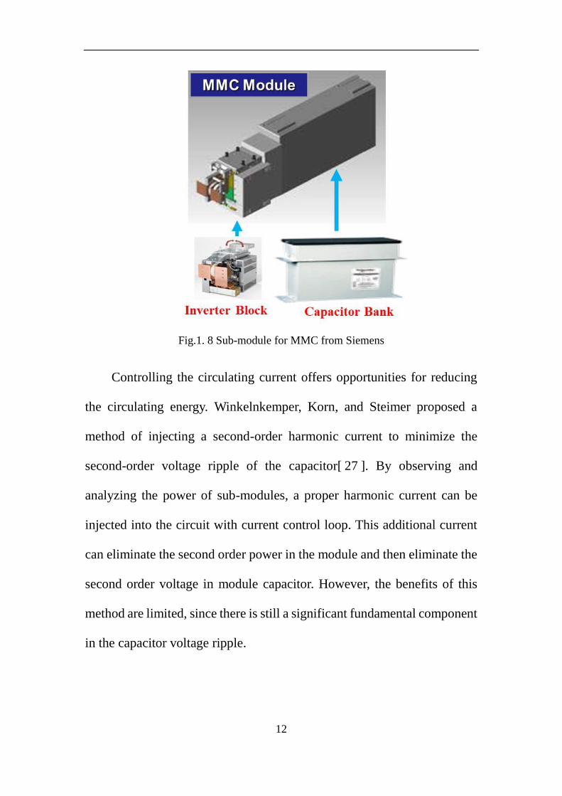
1.3. Challenges of Modular Multilevel Converter
Modular multilevel converters are being actively developed for
offshore wind or tidal power collection and onwards transmission. Given
the difficulties of constructing and maintaining an infrastructure in a hostile
environment, it is important to keep the size as low as possible. In the
current designs of an MMC submodule (SM) for 50 or 60 Hz ac grid-
connected systems, the reservoir capacitor needs to absorb low order
harmonics and hence accounts for over 50% of the total size and 80% of
weight[26]. For most time, the energy buffering capability of the capacitor
is not well utilized. The SM capacitor needs to be large enough
(capacitance) to constrain the voltage ripple, while having sufficient ripple
current capability to avoid overheating. Metalized polypropylene film
(MPPF) capacitors are commonly used in MMC SMs due to their stability
and ripple current capability. The sub-modules of Siemens is shown in Fig.1.
8. In most industry products, the volume of the capacitors is more than 50%
of the volume of the MMC. Hence, a method of reducing the circulating
energy and capacitor voltage ripple has been widely pursued as an
important research topic.
12
Fig.1. 8 Sub-module for MMC from Siemens
Controlling the circulating current offers opportunities for reducing
the circulating energy. Winkelnkemper, Korn, and Steimer proposed a
method of injecting a second-order harmonic current to minimize the
second-order voltage ripple of the capacitor[ 27 ]. By observing and
analyzing the power of sub-modules, a proper harmonic current can be
injected into the circuit with current control loop. This additional current
can eliminate the second order power in the module and then eliminate the
second order voltage in module capacitor. However, the benefits of this
method are limited, since there is still a significant fundamental component
in the capacitor voltage ripple.

13
The concept of injecting high-frequency voltage and circulating
current was proposed in [28] to facilitate the start-up of induction motors
with quadratic-torque loads. However, [28] only considers the dc and
fundamental components in the arm current, and ignores the second-order
component. Furthermore, the calculated circulating current is very
complex and contains both low frequencies and high frequencies.
Recently, a novel concept of controlling the modulation was proposed
to eliminate both the fundamental and second-order harmonic. The concept
comes also from power analysis; the modulation index is related to the
fundamental power in module. By setting a proper modulation index value,
the fundamental power in module and fundamental voltage ripple in
capacitor can be eliminated. In this method, full bridge module is required.
It should be noted that that even though there have been various
methods proposed to reduce the capacitor voltage ripple, it was mostly
done by trial and error. There is a lack of systematic approaches of
addressing the means for capacitor ripple reduction. In general, the
reported findings utilize the module power as a means to develop a control
strategy. However, the minimum power flow needed from the source
through the modules to the load is rather ambiguous.
14
A method of state trajectory analysis with the objective of delineating
the needed power flow from the unwanted circulating energy is proposed
in this thesis. The analysis method offers a graphical visualization of the
effectiveness of the various proposed methods. Furthermore, it leads to a
new proposed method that dramatically reduces the bulk of the circulating
energy by eliminating both the fundamental and second-order harmonic
components of power.
1.4. Thesis Outline
Taking into account the challenges raised during the literature survey
on the modular multilevel convertor, several issues have been addressed in
this thesis:
In Chapter 1, Research background, application, motivation,
challenges and opportunities are stated.
Due to the frequency flexibility and the cost saving for long distance
transmission, the DC transmission line is more competitive in high voltage
grid.
With the developing of semiconductor device, the new generation
MOSFET and IGBT give one the opportunity to connect high voltage DC
grid and AC grid by voltage source converters. Recently, the method of

15
using floating capacitor instead of the voltage source and bulky transformer
was proposed, the modular multilevel convertor becomes most prominent
interface converter used between DC and AC grid
The challenge of modular multilevel converter is that a large
capacitance is required in order to suppress the voltage ripple. Therefore,
reducing capacitor voltage attract lots of attention. However, there is a lack
of systematic approaches of addressing the means for capacitor ripple
reduction. This thesis also offers a graphical visualization of the
effectiveness of the various proposed methods.
In Chapter 2, Basic working principle and structure of MMC is
introduced
Pules width modulation and nearest level modulation are most
popular modulation method for MMC. Moreover, PWM could suppress all
low-order harmonics for multilevel converters and produce a sinusoidal
output for MMC.
Average balance control and individual balance control are the basic
control loop for MMC. With the basic control, the capacitor voltage of
difference sub-modules is in the same level, which is the foundation of
MMC basic operation and other control objects.

16
In order to analyze the working process clearly, MMC system can be
simplified to one phase with only one module per arm. Basing on the PWM
modulation and basic control, the complicated power flows in the MMC
circuit is in-depth studied.
In Chapter 3, the State trajectory analysis is proposed. It enables one
to gain a better understanding of the working principle of the MMC and
offers a simple way to assess the effectiveness of the various control
strategies with visual support.
Modulation index control method is proposed to reduce the
fundamental voltage ripple and analyzed with state space analysis as the
example 4
In Chapter 4, the concept is extended to the multi modules three phase
system. And the loss evaluation offers one the trade of between
semiconductor loss and voltage ripple reduction
The scaled down MMC hardware is introduced to verify the proposed
concept and enlighten one new research opportunities.
Finally, summary and future work are provided

17
Chapter 2 Basis Working Principle
2.1 Structure of MMC
Fig.2. 1 shows a three-phase MMC system with only a resistive load.
The neutral point ‘o’ on the dc side is a fictitious point which divides the
dc voltage to two equal parts of 0.5Vdc. The converter topology consists of
six phase arms. Each phase has an upper and a lower arm. There are n
series-connected modules with an arm inductor in each arm. Each module
has two switch devices and a capacitor in a half-bridge structure. In Fig.2.
1, the output is resistive and there is a neutral point ‘m’ of the three phases
of the load. The n modules per arm can provide n+1 voltage levels.
Fig.2. 1 Three phase MMC system
o
0.5Vdc
0.5Vdc
a
+vc1
+vcN
+vc(N+1)
+vc2N
b
+
+
+
+
c
+
+
+
+
m
R0

18
2.2 Pulse Width Modulation for MMC
The phase-shifted carrier-based PWM (PSC-PWM) method can
naturally suppress all low-order harmonics for multilevel converters[29].
The details of the modified PSC-PWM method for one pair modules in
upper and lower arm are shown in Fig.2. 2. The reference waveform for
upper and lower arm is complementary. Comparing the carrier duty cycle
waveform (vp_ref , vn_ref) with the triangle wave, the signal state condition of
upper and lower module can be achieved. When half-bridge module is used,
there are two switching states. The ‘1’ state denotes when the upper switch
is “on” and lower switch is “off;” the dc storage capacitor is connected in
the phase. The ‘0’ state denotes when the lower switch is “on” and the
upper switch is “off.” In the “0” state, the capacitor is bypassed from the
phase arm. With the state condition of upper and lower module (S1 and S2),
a sinusoidal output can be generated.

19
Fig.2. 2 PWM modulation for MMC with one module per arm
For an MMC with N number of SMs per arm, the reference arm
voltages are compared with triangular carriers, each phase shifted by an
angle of 360 degrees/N. As shown in Fig.2. 3. Compare with the same arm
duty cycle wave, each module achieves their own switch state condition.
Furthermore, in a N modules per arm MMC, the output voltage has N+1
level[ 30 ]. With 120 degrees’ phase shift on reference wave, this
modulation method can be extended to three phases system.

20
2 4 6 8 10 12 14 160
0.2
0.4
0.6
0.8
1
2 4 6 8 10 12 14 16
2 4 6 8 10 12 14 16-4
-2
0
2
4
Time/s
carr_pa1 carr_pa2 carr_pa3 carr_pa4
pa_ref
carr_na1 carr_na2 carr_na3 carr_na4
na_ref
ao
0
0.2
0.4
0.6
0.8
1
Fig.2. 3 PWM for multi modules per arm MMC
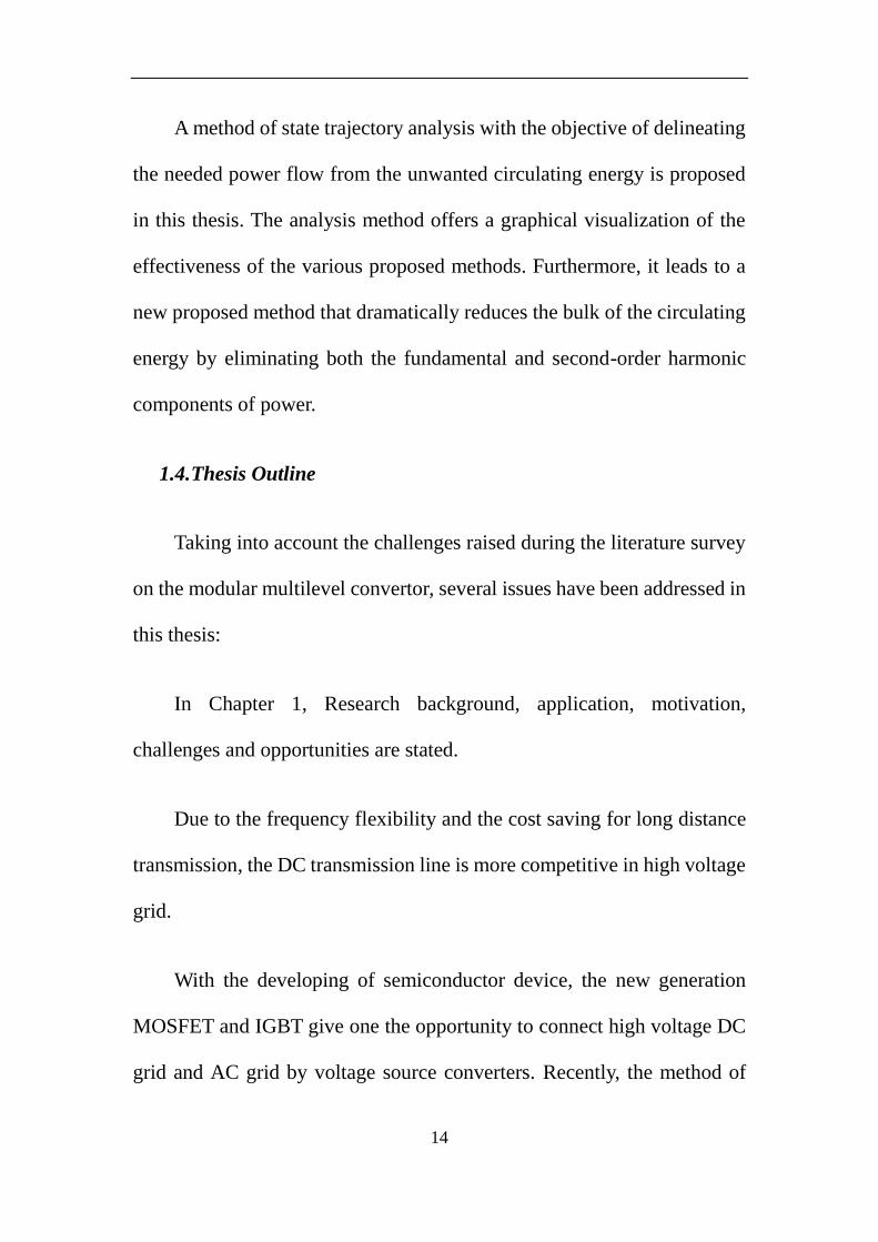
2.3 Nearest Level Modulation for MMC
Another effective modulation method is nearest level
modulation[ 31 ][ 32 ]. Fig.2. 4 illustrates the working principle of the
conventional NLM, with N module in one phase arm. The voltages are
normalized by Vc to indicate the number of inserted SMs. The resulting
output voltage va has a maximum level number of N + 1, with a step size
of Vc and largest possible error of 0.5vc. The waveforms of the upper and
lower arm step voltages Vpa_ref and Vna_ref are symmetrical to each other
21
with respect to the vertical y = N/2 line (suppose the normalized voltage
axis is the y-axis). Therefore, all the transition instants of Vpa_ref and Vna_ref
are aligned.
Fig.2. 4 working principle of the NLM
The control diagram of the conventional NLM method is illustrated
in Fig.2. 5 The voltage reference is first normalized by the sub-module
capacitor voltage vc, then the round function gives the closest integer
number of SMs to insert in order to approximate the voltage reference with
the nearest voltage level. The nearest integer function or round function, is
defined such that round(x) is the integer closest to x. The additional
convention is that half-integers are always rounded to even number [33],
for example round (1.5) = 2. The inserted upper and lower arm sub-module

22
numbers are:
_( )
2
A ref
low
dc
NVNn round
V (2.1)
_( )
2
A ref
up
dc
NVNn round
V
(2.2)
Fig.2. 5 The control diagram of NLM
The voltage balancing control is based on module voltage sorting. As
shown in Fig.2. 6. , according to the sensed module voltage and arm current
direction, N modules with highest voltage or lowest voltage are connected
with phase arm. The inserted modules number N is based on the calculation
in (2.1) and (2.2).
Fig.2. 6 The voltage balancing control of NLM

23
In the following simulation and analysis in this thesis, the pulse width
modulation is used due to its flexibility and stability, especially for MMC
with small module number.
2.4 Basic control loop for voltage balancing in MMC
Due to the large number of sub-modules and floating capacitors in
modules, the voltage balancing of modules is an important issue. The first
goal of voltage balancing is avoiding the over charge of the capacitor.
Furthermore, balanced capacitor voltage is also an assumption for
conventional modulation. Recent years, the solutions for this problem have
been found and proposed in many literature such as [34][29].
The basic voltage-balancing control can be divided into:
1) Averaging control; and
2) Individual balancing control.
Averaging Control:
Fig.2. 7 shows a block diagram of the averaging control. It forces the
one phase average voltage Vc_avr to follow its command Vcref, where Vc_avr
is given by
_ _
1
1 N
c avr c j
j
V VN
(2.3)

24
Let a dc-loop current command of iZref be iZ, as shown in Fig.2. 7. iZref
is a result of a PI functioned compassion between Vc_avr and Vcref . iz is the
current which go through the upper and lower arm at the same time (so
called “circulating current”). Vref_avr is the voltage command obtained from
the averaging control.
-
Vcref
Vc_avr
+ Vref_avr
PI -+
iZref
iP
iN
PI
12
iZ
Fig.2. 7 control diagram for average balance control
When Vcref ≥Vc_avr, iZref increases. The function of the current minor
loop forces the actual dc-loop current iZ to follow its command iZref . As a
result, this feedback control of iZ enables Vc_avr to follow its command Vcref
without being affected by the load current io .
Individual balancing control.
The use of the balancing control described in [35]forces the individual
capacitor voltage to follow its command Vcref . Fig.2. 8 shows a block
diagram of the individual balancing control, where vref_Ij is the voltage
command obtained from the balancing control. It forms an active power
between the voltage at the low voltage side of each sub-module, vj and the
corresponding arm current. Since the balancing control is based on either
iP or iN, the polarity of vref_Ij should be changed according to that of iP or iN.
25
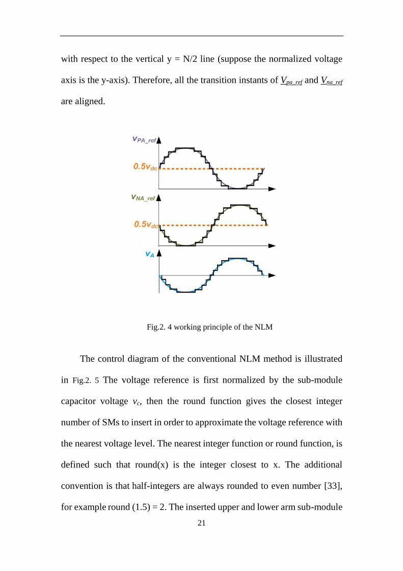
When Vcref≥ vj in the upper arm, a positive active power should be
taken from the dc power supply into the upper sub-modules. When iP is
positive, the product of vref_Ij and iP forms the positive active power. When
iP is negative, the polarity of vref_Ij should get inverse to take the positive
active power.
-
Vcref
vcj
+vref_Ij
K ±1
i
Fig.2. 8 control diagram of individual balance control
The finial reference capacitor voltage is represented as
_ _*ref ref avr ref Ij refv v v v (2.4)
where vc_avr comes from the average control loop, vref_Ij is a result of
individual balancing control. The vref is the original reference voltage. With
the basic control method mentioned above, the fundamental function of
MMC with multi sub-modules can be achieved.
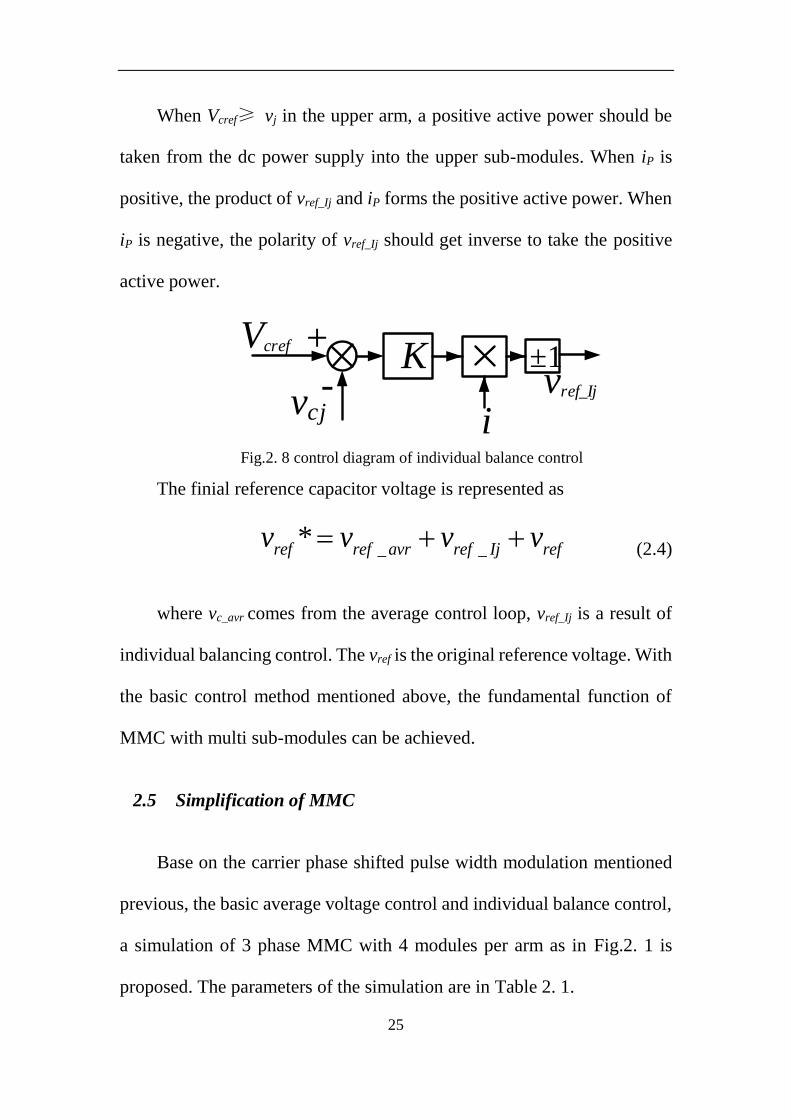
2.5 Simplification of MMC
Base on the carrier phase shifted pulse width modulation mentioned
previous, the basic average voltage control and individual balance control,
a simulation of 3 phase MMC with 4 modules per arm as in Fig.2. 1 is
proposed. The parameters of the simulation are in Table 2. 1.
26
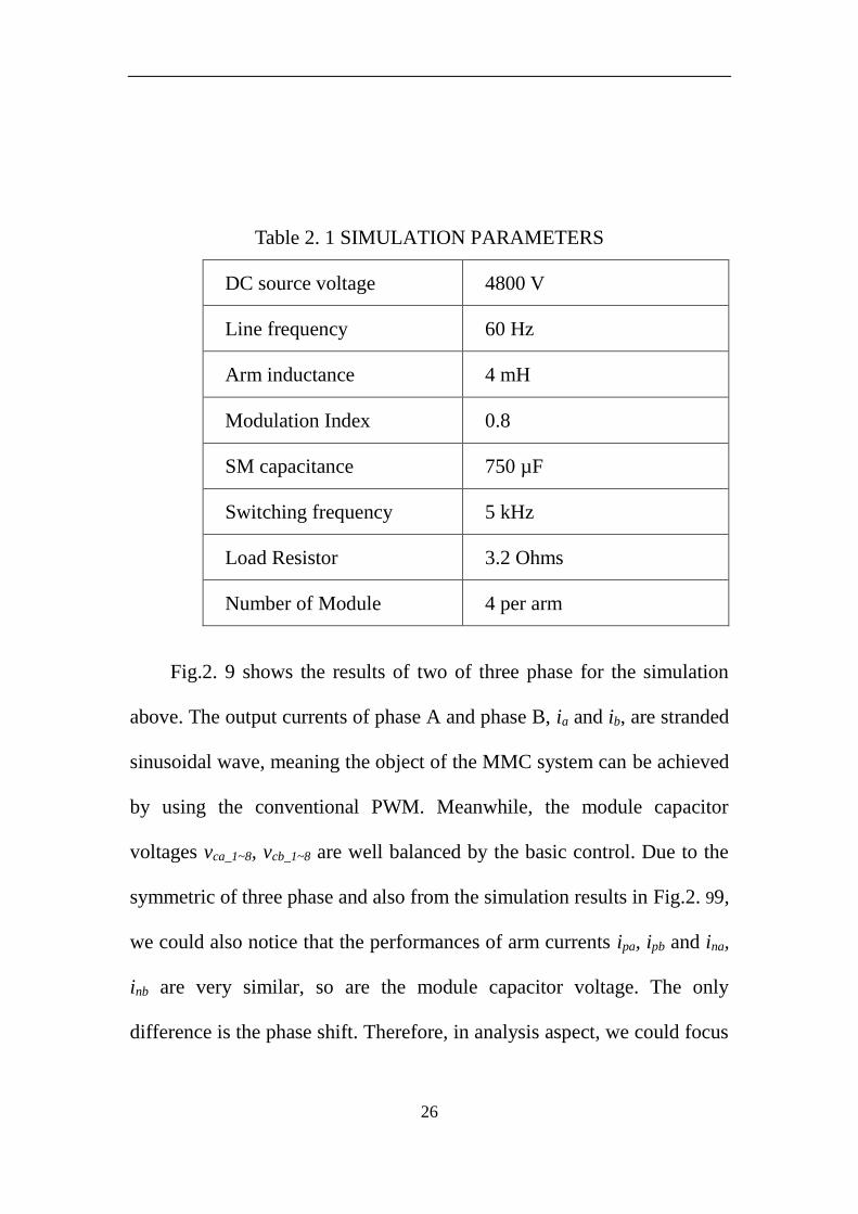
Table 2. 1 SIMULATION PARAMETERS
DC source voltage 4800 V
Line frequency 60 Hz
Arm inductance 4 mH
Modulation Index 0.8
SM capacitance 750 µF
Switching frequency 5 kHz
Load Resistor 3.2 Ohms
Number of Module 4 per arm
Fig.2. 9 shows the results of two of three phase for the simulation
above. The output currents of phase A and phase B, ia and ib, are stranded
sinusoidal wave, meaning the object of the MMC system can be achieved
by using the conventional PWM. Meanwhile, the module capacitor
voltages vca_1~8, vcb_1~8 are well balanced by the basic control. Due to the
symmetric of three phase and also from the simulation results in Fig.2. 99,
we could also notice that the performances of arm currents ipa, ipb and ina,
inb are very similar, so are the module capacitor voltage. The only
difference is the phase shift. Therefore, in analysis aspect, we could focus

27
on only one phase instead of three phases. In the following discuss in this
thesis, the analyses are mainly based on one phase system.
Fig.2. 9 Simulation results of three phase MMC
(2.5)
1 0 01
1 1
2 0 0 1 2
1 1
22
0 0
0 0 0 0 0
0 0 0 0 0
0 0 0 0 0
0 0
0 0 0 0 0
0 0 0 0 0
0 0 0 0 0
N
c
cN N
N N
c N N
Nc N
di R d Rd
dt L L L L
dv d
dt C
dv d
dt C
di R R d d
dt L L L L
dv d
Cdt
ddv
Cdt
1
1
2
1
2
2
0
0
2
0
0
dc
c
cN
dc
c N
c N
Vi Lv
v
i V
v L
v

28
The matrix above is the differential equations of a single-phase
MMC with N sub-modules in phase. In terms of the matrix, the upper arm
and lower arm equation are coupled by the term in the red box, which
contains only the components of load.
(2.6)
Equation (2.6) is the expression of the output current. Substituting
(2.6) into matrix (2.5), a decoupled matrix can be achieved, as follows
below.
(2.7)
In (2.7), with considering the load components as given value and
moving them into the constant matrix, all the terms in the red boxes are
zero, meaning that the matrix can be seen as two decoupled parts. The
0/o oi v R
1 1
1 1
2 1 2
1 1
22
0 0 0 0
0 0 0 0 0
0 0 0 0 0
0 0 0 0 0
0 0 0 0
0 0 0 0 0
0 0 0 0 0
0 0 0 0 0
N
c
cN N
N N
c N N
Nc N
di dd
dt L L
dv d
dt C
dv d
dt C
di d d
dt L L
dv d
Cdt
ddv
Cdt
1
1
2
1
2
2
0
0
2
0
0
dc ao
c
cN
dc ao
c N
c N
V vi L Lv
v
i V v
v L L
v

29
upper part of the equation represents the upper arm information of the
circuit, and the lower part of the equation stands for the lower arm.
(2.8)
Matrix (2.8) is the upper part of (2.7), which contains the upper arm
information. If all the duty cycles d are assumed as same value and all
capacitor voltages vc are well balanced, the information in this complex
system can be represented by a 2X2 matrix in the red box.
Basing on the decoupling concept above, the multi module circuit
can be represented by the simplified circuit with only one module per
arm, showing in Fig.2. 10 . The differential equations of the simplified
circuit are represented as:
1 1
1
111
0
2
00
dc o
cc
di dV v
idt LL L
vddv
Cdt
(2.9)
1 1
1
1 11
0
20 0
0
0 0
00 0
N
dc ao
cc
cNNcN
di dd
V vdt L L iL Ldv d
vCdt
vddv
Cdt

30
2 2
1
212
0
2
00
dc o
cc
di dV v
idt LL L
vddv
Cdt
(2.10)
Fig.2. 10 Simplified one phase MMC circuit with one module per arm
Fig.2. 11 Replacing switching model with average model in MMC
Our analysis in this thesis is focused on the line frequency problems,
the switching frequency performance of the circuit is not our concern.
Therefore, as in Fig.2. 11 the switching model can be replaced with the
average model with the following equations:

31
sm C
C arm
v S v
i S i
(2.11)
p C
C arm
v d v
i d i
(2.12)
2.1 Analysis of simplified MMC circuit
Fig.2. 12 is the simplified one module circuit with average model. The
ac reference output voltage and current can be defined as:
(2.12)
(2.13)
where M is the modulation index.
Fig.2. 12 The average circuit model with current loop
0.5 cos( )o dcv V M t
0.5 cos( ) /o dci V M t R

32
In the conventional open-loop control law of the MMC, the duty cycle
of the upper module d1 and lower module d2 is set based on Kirchhoff’s
voltage law (KVL).
(2.14)
where vc1 and vc2 are the sub-module capacitor voltages. For the
purpose of defining a simple modulation control law, one can first assume
that the voltage ripples of the sub-module capacitor voltage are negligible.
Hence vc1 and vc2 are replaced by Vdc. Furthermore, because the arm
inductor is a relatively small value, the voltage on the inductor can also be
neglected. Thus the expression of duty cycle can be written as
(2.15)
In the circuit in Error! Reference source not found., due to the KCL,
he currents have the following relationship.
(2.16)
(2.17)
(2.18)
where the upper arm current is i1, the lower arm current is i2 and output
1 1
2 2
0.5
0.5
dc c o L
dc c o L
V d v v v
V d v v v
1
2
0.5 0.5 cos
0.5 0.5 cos
d M t
d M t
1 2oi i i

33
current is io. From (2.17) and (2.18), we know that the arm currents i1 and
i2 have three components. One of the components is from half the output
current io, the green loop in Fig.2. 12. The other two components are the
currents which do not go to the output, but go through from the upper arm
to the lower arm and circulate in the circuit. In the Fig.2. 12, the circulating
current is in orange color. Variable ihar represents the low-frequency
harmonics. Since ihar does not flow into the load, ihar offers a free variable
to control.
With the simple duty cycle control law in (2.15), a simulation of the
circuit in Fig.2. 12 was made to observe the base performance of this
simplest case with the simulation parameters in Table 2. 2.
Table 2. 2 SIMULATION PARAMETERS
DC source voltage 600 V
Line frequency 60 Hz
Arm inductance 2 mH
Modulation Index 0.8
SM capacitance 750 µF
Switching frequency 5 kHz
Load Resistor 3.2 Ohms
The simulation results are shown in Fig.2. 13. The output voltage is a
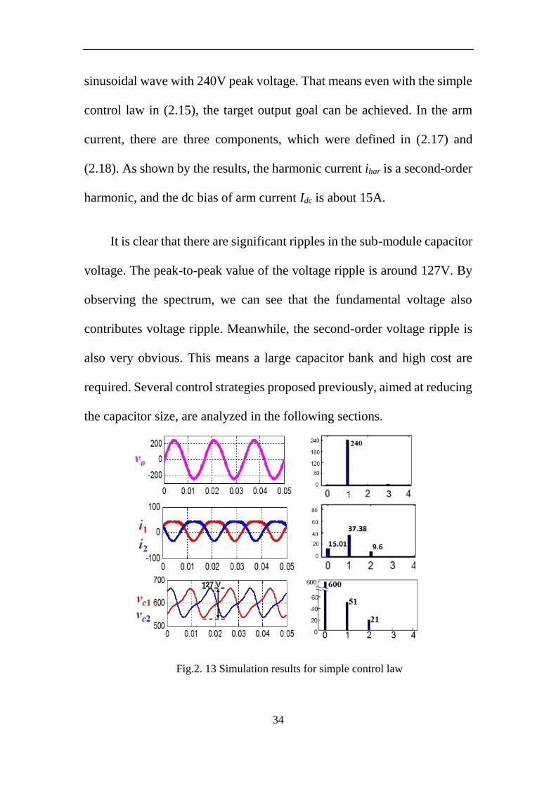
34
sinusoidal wave with 240V peak voltage. That means even with the simple
control law in (2.15), the target output goal can be achieved. In the arm
current, there are three components, which were defined in (2.17) and
(2.18). As shown by the results, the harmonic current ihar is a second-order
harmonic, and the dc bias of arm current Idc is about 15A.
It is clear that there are significant ripples in the sub-module capacitor
voltage. The peak-to-peak value of the voltage ripple is around 127V. By
observing the spectrum, we can see that the fundamental voltage also
contributes voltage ripple. Meanwhile, the second-order voltage ripple is
also very obvious. This means a large capacitor bank and high cost are
required. Several control strategies proposed previously, aimed at reducing
the capacitor size, are analyzed in the following sections.
Fig.2. 13 Simulation results for simple control law

35
In [16], the reason for the capacitor voltage ripple is explained. The
module plays a significant role for power transfer in this circuit. As
explained in [16], the module must produce a power offering to load or
transfer with the source and even other modules. The produced power has
harmonics. However, the only component which can carry that harmonic
power is the capacitor. The inductor voltage and inductor power, which are
very small, will be assumed to be negligible. In order to analyze this issue
clearly, a power flow analysis is necessary. In following power analysis,
the inductor voltage and inductor power are ignored.
(2.19)
(2.20)
where pp is the upper module power and pn is the lower module power,
and i1 and i2 are the arm current, vpa is the upper arm voltage from point p
to point a, and van is the lower arm voltage. Using the KVL, the expression
of vpa and van can be derived:
(2.21)
(2.22)
Substituting (2.17) and (2.21) into (2.19) and substituting (2.18) and
(2.22) into (2.20), the expression of the arm power can be calculated:
(2.23)
(2.24)
1p pap i v
2n anp i v
0.5 cospa dc ov V V t
0.5 cosan dc ov V V t
1 1 1 1 1( )cos cos 2 cos32 2 4 2 2
p o dc dc o h o o o har dc h op I V I V I V t V I t i V I V t
1 1 1 1 1( )cos cos 2 cos32 2 4 2 2
n o dc dc o h o o o har dc h op I V I V I V t V I t i V I V t

36
In (2.25), it describes the relationship of the upper module power and
arm current. The components in (2.25) in orange color are associated with
the orange part in (2.17), which are “circulating current”. The components
in (2.25) in green color are associated with the green part in (2.17) which
are load current. Based on the common understanding of circulating
current, the circulating current produces the circulating power. However,
the question is: In this circuit, is all the circulating power produced by
circulating current? In order to answer this question, power flow analysis
is required.
(2.25)
To understand the function and relationship of power flows, the load
power and total source power also need to be observed.
(2.26)
(2.27)
where po is the load power which has a dc term and an ac term, and ps
is the total source power, which also has a dc term and an ac term.
By observing the equations above, we can summarize several
relationships.
1 1cos 2
2 2o o o o op I V I V t
1 2
1 1( )
2 2s dc o o har dcp V i i I V i V

37
a) The dc term in po equals the dc terms in ps;
b) The second-order harmonic ac term in the load power equals
twice the second-order harmonic term in the upper and lower arm power;
c) The ac power in the source, which relates to ihar, equals to the
harmonic term in the arm power;
d) In the upper arm power and lower arm power equations, the
fundamental and third-order harmonic components have opposite signs.
Even though the power transfer process in this circuit is very
complicated, we can derive the following observations:
a) The dc power in the load comes from the source;
b) The phase arm contributes second-order power to the load;
c) The phase arm receives power from the source;
d) The AC power switches between the upper arm and lower arm.
The power flow analysis above can be shown in Fig.2. 14. Moreover,
the relationship of arm current and module power is summarized in Table
2. 3. By observing the table, we could notice that the circulating harmonic
power is associated with all the components of arm current, not only the so

38
called “circulating current”.
Fig.2. 14. Power transfer diagram
Table 2. 3 SUMMARY OF ARM CURRENT AND MODULE POWER
Using Fig.2. 14 and Table 2. 3 , the function of the modules can be

39
explained in terms of energy storage and transfer. It can be noted that the
module has a significant role in the power flow process for this circuit.
However, the amount of energy storage and transfer that is essential for the
intended purpose is still unknown. In the sections below, the state
trajectory analysis is employed to help minimize the circulating power and
thus minimize the voltage ripple.

40
Chapter 3 State Space Analysis
3.1 Introduction of State Space Analysis
In the previous section, Fig.2. 13 shows that the arm current and
capacitor voltage are the state variables in each module. Hence the four
state variables for the MMC are defined as i1, i2, vc1, and vc2. Because i1
and i2 are related by (3.1), they are not independent. Therefore, there are
only three independent variables. Thus, one can use a 3D state trajectory,
with the three variables i1, vc1, and vc2 to represent the system.
(3.1)
Fig.3. 1 illustrates the 3D state trajectories. To facilitate visual support,
the 3D state trajectory is projected into three 2-D planes, as shown in Fig.3.
2.
1 2 oi i i

41
Fig.3. 1 3D state space diagram for MMC
Fig.3. 2 2D state plane projection for MMC
The capacitor voltage of upper and lower module can be calculated
using (6) and (7).
42
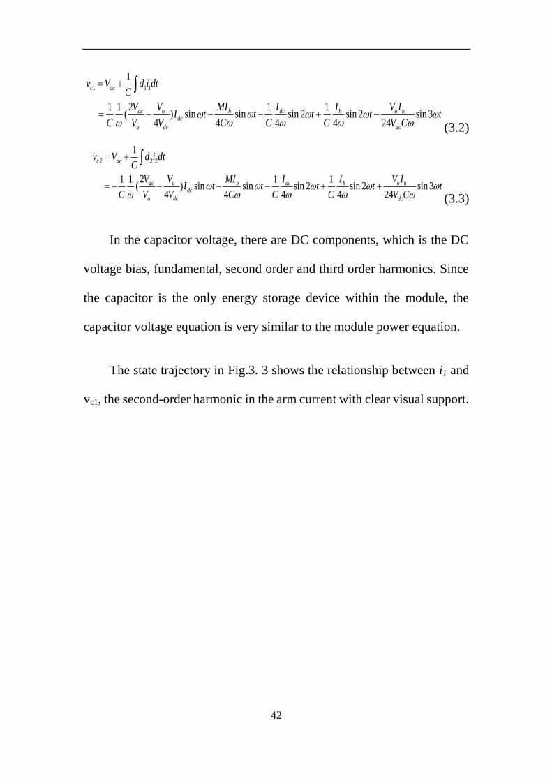
(3.2)
(3.3)
In the capacitor voltage, there are DC components, which is the DC
voltage bias, fundamental, second order and third order harmonics. Since
the capacitor is the only energy storage device within the module, the
capacitor voltage equation is very similar to the module power equation.
The state trajectory in Fig.3. 3 shows the relationship between i1 and
vc1, the second-order harmonic in the arm current with clear visual support.
1 1 1
1
21 1 1 1( ) sin sin sin 2 sin 2 sin 3
4 4 4 4 24
c dc
dc o h dc h o hdc
o dc dc
v V d i dtC
V V MI I I V II t t t t t
C V V C C C V C
2 2 2
1
21 1 1 1( ) sin sin sin 2 sin 2 sin 3
4 4 4 4 24
c dc
dc o h dc h o hdc
o dc dc
v V d i dtC
V V MI I I V II t t t t t
C V V C C C V C

43
Fig.3. 3 The state plane trajectory of upper arm current and module voltage
The size of the state trajectory in one cycle of operation is proportional
to its energy; i.e., a larger loop leads to a higher energy content. For
example, illustrates that the loop size decreases with a larger load resistor.
Fig.3. 4 shows the state trajectory of i1 and vc1with different power ratings

44
Fig.3. 4 State trajectory of i1 and vc1 with different power rating
Fig.3. 5 shows the 2D state trajectory in terms of the vc1 and vc2 planes
and the voltage waveform. The state trajectories cross paths during one-
line cycle, symptomizing the energy exchange between modules. The
waveform and trajectory can be separated to two parts. In blue interval the
voltage in upper and lower module change in different direction, that
means when one increases the other one decreases. In red interval the
voltage in upper and lower module change in same direction, when one
increases or decreases the other one also increases or decreases.

45
Fig.3. 5 2D state trajectory of the vc1 and vc2 planes and waveforms
To explain this phenomenon, two axes are defined; the α-axis and the
β-axis. The α-axis denotes the energy storage related to odd-order
harmonics, which is associated with the blue interval in waveform. On the
other hand, the β-axis is related to even-order harmonics, which is
associated with the red interval in waveform. The above statements are
supported by examining (3.2) and (3.3). In (3.2) and (3.3), the
fundamental and third-order harmonics are represented with the opposite
sign, meaning energy exchanges between these two modules. The second-
order harmonics are represented with the same sign, meaning energy is
stored in the modules and eventually delivered out of the power phase.
If we use the power flows analysis in Fig.2. 14 as cross reference, we

46
could find that the α-axis is related to power swapping between modules
and the β-axis is related to power exchange between module and source or
load.
3.2 State Trajectory Analysis for Different Control Method
In this sub-section, the proposed state-trajectory analysis is employed
to evaluate the effectiveness of various control strategies with the intent of
minimizing circulating energy and the bulk capacitor.
Example 1: Simple control law
The simple control law used in the previous section is employed here
as the first example to illustrate the power flow analysis. As noted in Fig.2.
13, the module has a significant role in energy storage and transfer for the
system. Fig.2. 14 and Table 2. 3 shows the relationship between the arm
current and the associated module power, which is broken down in terms
of dc, fundamental components and harmonics.
47
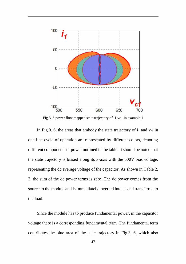
Fig.3. 6 power flow mapped state trajectory of i1 vc1 in example 1
In Fig.3. 6, the areas that embody the state trajectory of i1 and vc1 in
one line cycle of operation are represented by different colors, denoting
different components of power outlined in the table. It should be noted that
the state trajectory is biased along its x-axis with the 600V bias voltage,
representing the dc average voltage of the capacitor. As shown in Table 2.
3, the sum of the dc power terms is zero. The dc power comes from the
source to the module and is immediately inverted into ac and transferred to
the load.
Since the module has to produce fundamental power, in the capacitor
voltage there is a corresponding fundamental term. The fundamental term
contributes the blue area of the state trajectory in Fig.3. 6, which also

48
relates to the blue terms in Table 2. 3. As explained above, this fundamental
power switches to the lower arm, showing in Fig.2. 14. Since the net Pp(ωt)
is not zero, the capacitor needed to store energy is related to the
fundamental frequency. The green area in Fig.3. 6 is caused by second-
order harmonic power. This Pp(2ωt) also produces the second-order
voltage ripple in the capacitor. A portion of this power is associated with
the green terms in Table 2. 3 and eventually transferred to the load,
showing in Fig.2. 14. The second portion of Pp(2ωt), marked in orange, is
the result of energy coming from source. This component of the power is
further examined in Fig.2. 14.
Fig.3. 7 power flow mapped state trajectory of i1 vc1 in example 1
In Fig.3. 7, the fundamental power in Table 2. 3 and the fundamental
component of the voltage contribute the blue line in the state trajectory. If

49
we consider both the upper arm and lower arm, the trajectory without any
distance in β-axis means that power does not transfer out of phase nor
transfer to the load nor source. This fundamental power only transfers
between the arms. However, this power does make a voltage ripple in the
capacitor, as shown in Fig.2. 143.
The green area in Fig.3. 7 represents the energy stored in the module
and eventually transferred from the module to the load. It is colored in
green in Table 2. 3 as well as in Fig.2. 14. Because this voltage ripple is a
second-order harmonic, it extends the trajectory in the β-axis. As discussed
above, the area indicates the power the phase arm contributes to the load.
Since the module also transfers power to the source, additional Pp(2ωt)
power is stored in the capacitor and indicated by the orange area in Fig.3.
7. and Table 2. 3. There is also a small amount of Pp(3ωt) alone the α-axis.
From the diagram, it can be seen that the fundamental component
contributes most of the voltage ripple in the α-axis.
Example 2: Zero harmonic current
A very popular control method is to eliminate the harmonic current
with the idea of minimizing circulating current [36]. If the harmonic arm
current is eliminated, the arm currents are:

50
(3.4)
(3.5)
With the harmonic current elimination, the voltage ripple in module
capacitor can be reduced, showing in Fig.3. 8
Fig.3. 8 simulation results of MMC with harmonic current elimination
From Fig.3. 8, we could notice that arm current has only DC part and
fundamental part. As a result, the cap voltage ripple is also reduced. The
fundamental, 2nd order are all smaller and the 3rd order harmonic is
eliminated. Meanwhile, the phase modules power is defined as
(3.6)
1 0.5 o dci i I
2 0.5 o dci i I
1 1( )cos cos 22 4
p o dc dc o o op I V I V t V I t

51
(3.7)
Using TABLE 3. 1 and Fig.3. 9, the function of the module power can
be clearly explained. The module provides dc and Pp(2ωt) power to the
load and the Pp(ωt) power switches between the upper and lower arms. In
this example, the module no longer exchange power with the source.
Fig.3. 9 Power transfer diagram for ihar=0
1 1( )cos cos 22 4
n o dc dc o o op I V I V t V I t
52
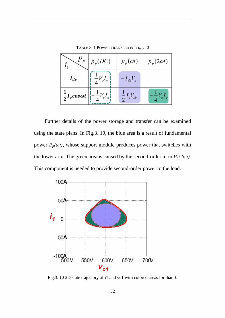
TABLE 3. 1 POWER TRANSFER FOR IHAR=0
Further details of the power storage and transfer can be examined
using the state plans. In Fig.3. 10, the blue area is a result of fundamental
power Pp(ωt), whose support module produces power that switches with
the lower arm. The green area is caused by the second-order term Pp(2ωt).
This component is needed to provide second-order power to the load.
Fig.3. 10 2D state trajectory of i1 and vc1 with colored areas for ihar=0

53
Fig.3. 11 2D state trajectory of vc1 and vc2 with colored area for ihar=0
Fig.3. 11 shows that the fundamental voltage extends the trajectory in
the α-axis, which causes the energy exchange between the two modules,
denoted by the blue line. The green area is caused by the second-order
voltage, which extends the trajectory in the direction of the β-axis. This
area represents the energy stored in the capacitor related to Pp(2ωt), which
is transferred to the load.
Compared with Example 1, the area enclosed by the state trajectory is
smaller. Significant reduction of β energy and small reduction of α energy.
Since the module no longer needs to store energy that is eventually
transferred back to the source, the capacitor voltage ripple is reduced. In
this example the module still needs to store energy related to the

54
fundamental frequency and its second-order harmonic.
Example 3: Second-order harmonic current injection
As discussed above, the module supplies second-order harmonic
power to the load. If a proper amount of the second-order current is injected,
the module may not need to store the second-order harmonic-related
energy [36]. The proposed second-order harmonic current injection is:
(3.8)
With this harmonic current injection, the voltage ripple in module
capacitor can be reduced, showing in Fig.3. 8
Fig.3. 12 simulation results of MMC with 2nd order harmonic injection
With the harmonic current as 2nd order, the cap voltage ripple is
cos 2har dci I t

55
reduced. In cap voltage, the fundamental part is reduced, the 2nd order part
is eliminated, but introduced a small 3rd order part.
the second-order component of the module power as shown in (3.9)
and (3.10) will cancel out each other. That means the module does not
provide power to the load or to the source. The power equations are
simplified significantly:
(3.9)
(3.10)
Using Table 3. 2 and Fig.3. 13, the function of module power flow
can be clearly explained. The module only needs to store the Pp(ωt) needed
to switch between the upper and lower arms. All the load power comes
from the source. From Table 3. 2, we can observe that only the odd-order
power components exist in the module.
1 1 1( )cos cos32 2 2
p o dc dc o dc o dc op I V I V I V t I V t
1 1 1( )cos cos32 2 2
n o dc dc o dc o dc op I V I V I V t I V t

56
Fig.3. 13 Power transfer diagram for second-order current injection
TABLE 3. 2 POWER TRANSFER FOR SECOND-ORDER CURRENT INJECTION
Details of the power storage and transfer can be examined using the
state planes. In Fig.3. 14, the blue area is further reduced compared to
Example 2. The capacitor voltage consists of only the fundamental and
third-order harmonic voltages.

57
FIG.3. 14 2D state trajectory of i1 and vc1 with colored area representing second-
order harmonics
Fig.3. 15 clearly shows in this case the state trajectory only travels
along the α-axis; thus no even-order harmonics exists. As discussed above,
this means that no power transfers out of the phase module to the source or
load. The only circulating power that exists is Pp(2ωt) switching between
the arms. Moreover, due to the strong injected second order current, the
circle loop is not round like.

58
Fig.3. 15 2D state trajectory of vc1 and vc2 for second-order current injection
Compared with the previous cases, this case is more promising.
However, the main issue remains that the modules still need to store and
transfer line-frequency-related circulating energy; thus the capacitor bank
remains bulky.
Example 4: Controlling the modulation index
Observing the module power (3.9) (3.10), we could find that there is
only odd order harmonic power which contribute all the voltage ripple. In
(3.9),(3.10) the module power is a function of Vdc, Vo, Io and Idc.
Meanwhile, those four variables have relationship which is associated with
the modulation index M, as following representation:
(3.11) 2 /o dcM V V

59
Substitute (3.11) in to (3.9) and (3.10), the module power equation
can be rewritten as:
(3.12)
The expression of module power is a function of modulation index M.
When M changes, the power and voltage ripple also change, as shown in
Fig.3. 16.
Fig.3. 16 State plane with changing modulation index
As shown in Fig.3. 16, when M increases, the α energy decreases, that
1 3 1( ) cos cos32 8 8
1 3 1( ) cos cos32 8 8
p o o o o
n o o o o
p M I V t MI V tM
p M I V t MI V tM

60
can be also examined in (3.12). Our team have recently proposed a new
control strategy of controlling modulation index M while still injecting the
second-order harmonic current in the same way as Example 3. By over-
modulation one can further reduce the fundamental component of
circulating energy. If M = 1.15, the fundamental component of energy can
be totally eliminated and the capacitor size drastically reduced. Since the
modulation index is always less than one in the half-bridge module, the
concept can only be implemented in the full-bridge topology. Analyzing
the module power equations in the previous case, with M=1.15 they can
also be written as:
(3.13)
However, in half bridge module, the modulation index has limitation.
It cannot larger than 1. In order to increase M to 1.15, full bridge module
could be employed. As shown in Fig.3. 17. with full bridge module, the
modulation index is limitation free.
1cos3
8
1cos3
8
p o o
n o o
p MI V t
p MI V t

61
Fig.3. 17 modulation index control realized with full bridge module
With this modulation index control, the voltage ripple in module
capacitor can be reduced a lot, showing in Fig.3. 18
Fig.3. 18 simulation results for modulation index control

62
In cap voltage, the fundamental part is zero, the 2nd order part is
eliminated, still there is a small 3rd order part.
Under proposed control method, there is only a small amount of
circulating energy related the third-order harmonic, and it switches
between the upper and lower arms. From TABLE 3. 3 and we can observe
that most of the power terms are equal to zero; the only term left is a small
amount of third-order power.
Table 3. 3 Power transfer for Modulation Index control
Fig.3. 19. Power transfer diagram for M = 1.15

63
Fig.3. 20 illustrates that the area embodied by the state trajectory is very
small and related only to the third-order harmonic voltage.
Fig.3. 20 2D state trajectory of i1 and vc1 for M = 1.15
Fig.3. 21 shows the state trajectory of vc1 and vc2. The small state
trajectory is caused by the small third-order voltage. There is no
fundamental or second-order harmonic. The α energy and β energy are both
reduced near zero.
Fig.3. 21 2D state trajectory of vc1 and vc2 with colored area for M = 1.15

64
Compared with the previous cases, this case is much better. The
fundamental ripple is eliminated and there is only small third order
harmonic in capacitor voltage, whose effect is very limited. From the state
plane we could notice that in the Fig.3. 21, the voltage is fluctuating around
the middle point, that means most of the circulating power is eliminated in
this circuit.
In Fig.3. 22. a summary of proposed examples is plotted. It is obvious
that in our finial design, the modulation index control, the capacitor voltage
ripple can be significantly reduced and the circulating power in this circuit
is almost eliminated.
Fig.3. 22 comparison of state trajectory for different control strategies

65
Example 5: High-frequency injection for three-phase MMC
A more complicated case, the high frequency injection method was
proposed in [37] to reduce the capacitor voltage ripple. It was employed to
demonstrate the start-up of an induction motor with quadratic-torque loads.
However, it only considers the dc and fundamental components in the
branch current and ignores the second-order components, so the power
flow processes are very complex.
The author injected a high-frequency common-mode voltage in the
neutral point of the three-phase load. The structure of this method is shown
in Fig.3. 23. The high-frequency common-mode voltage is added between
point m and point o. This high-frequency voltage injection makes it
possible to eliminate the low-frequency harmonic power in the module.
Fig.3. 23 Three-phase MMC for high-frequency common-mode voltage injection
66
The power flow in the proposed method is rather complex to analyze,
but using the proposed state trajectory can help us gain some insight into
this approach.
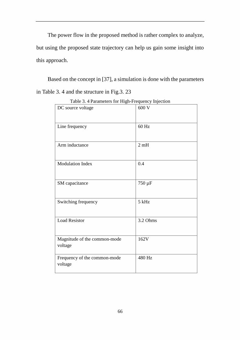
Based on the concept in [37], a simulation is done with the parameters
in Table 3. 4 and the structure in Fig.3. 23
Table 3. 4 Parameters for High-Frequency Injection
DC source voltage 600 V
Line frequency 60 Hz
Arm inductance 2 mH
Modulation Index 0.4
SM capacitance 750 µF
Switching frequency 5 kHz
Load Resistor 3.2 Ohms
Magnitude of the common-mode
voltage
162V
Frequency of the common-mode
voltage
480 Hz

67
Fig.3. 24 Simulation results of high-frequency common-mode voltage injection
The simulation results waveforms in Fig.3. 24 show that the high-
frequency capacitor voltage ripple dominates the voltage fluctuation. The
low-frequency voltage ripple is suppressed. The state trajectories of this
simulation are plotted in Fig.3. 25.

68
Fig.3. 25 State trajectory comparison of high-frequency injection and over-
modulation
Unlike Example 4, here the high-frequency injection method encircles
the quiescent point numerous times while the over-modulation method
only encircles it once in a line cycle. In both cases, the fundamental and
second-order line frequency components are invisible.

69
Fig.3. 26 comparison of high frequency injection, modulation index control and ideal
case
Fig.3. 26 plots three state plane for the best solutions and ideal case.
The high frequency injection method can suppress the voltage ripple a lot,
especially the low frequency harmonic voltage can be eliminated. However,
due to the injected high frequency common mode voltage, in one-line cycle,
the current fluctuates many times, meaning large conduction loss. On the
other hand, the modulation index control can provide an even smaller
voltage ripple with low frequency current and voltage fluctuation.
Comparing with the ideal case without any voltage ripple, the modulation
index control method can offer a near-perfect result.

70
Chapter 4 Verification of Concept
4.1 Concept extension to multi modules
In industry application, a MMC system contains numerous of sub-
modules. All the modules share the high DC link voltage. A scale downed
three phase MMC with 12 modules per arm is demonstrated in Fig.4. 1 for
implementing the concept to real case. The parameters are shown in Table
4. 1 The sub-modules in this circuit can be half bridge or full bridge.
Fig.4. 1 Circuit Structure for MMC with 12 module per arm

71
Table 4. 1 Parameters for simulation with 12 modules per arm
DC bus voltage 7.2kV
Power rating 1MW
Line frequency 60Hz
Arm inductor (L) 4.8mH
Module capacitance 900µF
Switching frequency 4800Hz
Modules per arm 12
Fig.4. 2 Simulation results for proposed control methods
Fig.4. 2 describes the simulation results of proposed voltage ripple
suppression methods. By observing the results, we could notice that the

72
concept of modulation index control and the other control methods work
well for multi modules case and they all can reduce the capacitor voltage
ripple. Fig.4. 3 gives us the summary of voltage ripple of the examples
proposed.
Fig.4. 3 summary of voltage ripple of the different control method
Base on the results in Fig.4. 3, with modulation index control, the
voltage ripple can be reduce 85%. That means with the same voltage ripple
tolerance standard, the capacitance can be reduced 85%. Therefore, in this
simulation circuit, the 900 μF capacitance can be replaced with 135 μF. For
industry application, small capacitance means saving money and space.
Especially for the MMC built in the offshore platform, the volume of bulky
capacitor is a significant issue.
However, in the design 4, in order to implement a modulation index
equals 1.15, full bridge modules have to be used. Hence, the conduction
loss is increased in this case. Base on the information of a 1.2kV IGBT
73
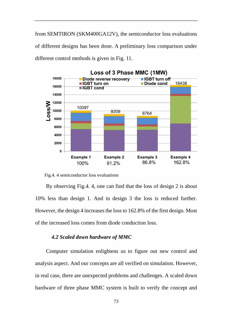
from SEMTIRON (SKM400GA12V), the semiconductor loss evaluations
of different designs has been done. A preliminary loss comparison under
different control methods is given in Fig. 11.
Fig.4. 4 semiconductor loss evaluations
By observing Fig.4. 4, one can find that the loss of design 2 is about
10% less than design 1. And in design 3 the loss is reduced further.
However, the design 4 increases the loss to 162.8% of the first design. Most
of the increased loss comes from diode conduction loss.
4.2 Scaled down hardware of MMC
Computer simulation enlightens us to figure out new control and
analysis aspect. And our concepts are all verified on simulation. However,
in real case, there are unexpected problems and challenges. A scaled down
hardware of three phase MMC system is built to verify the concept and

74
provide us inspiration of research outlook. The structure of the prototype
hardware is shown in Fig.4. 5.
Fig.4. 5 Structure of Scaled down MMC hardware
Shown as in Fig.4. 5, the system is a converter connected between DC
bus and AC output. It has 24 sub-modules which are separated to three
phases, meaning 8 modules per phase and 4 modules per arm. Each phase
has a DSP control board for most of the individual controlling. Moreover,
there is also a master control board to deal with the communication issue
between three phase and to give some general control order. The
parameters of this system are in Table 4. 2
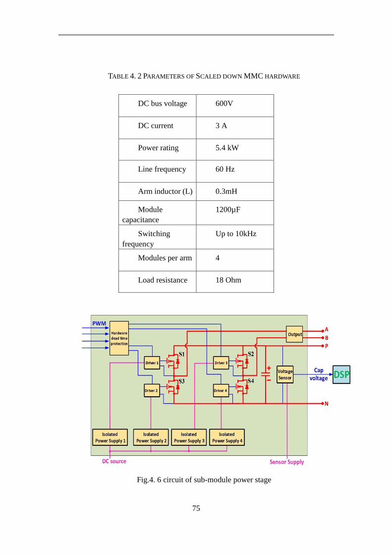
75
TABLE 4. 2 PARAMETERS OF SCALED DOWN MMC HARDWARE
DC bus voltage 600V
DC current 3 A
Power rating 5.4 kW
Line frequency 60 Hz
Arm inductor (L) 0.3mH
Module
capacitance
1200µF
Switching
frequency
Up to 10kHz
Modules per arm 4
Load resistance 18 Ohm
Fig.4. 6 circuit of sub-module power stage

76
The schematic of one sub-module is shown in Fig.4. 6. Four MOSFET
are driven by four individual gate driver which are supported by four
isolated power supply. The PWM signal are secured by the hardware
protection which can provide the dead time protection and make sure the
signals of upper switch and lower switch are complementary. The module
has two output mode. When P and N are connected to the arm, the module
works as half bridge. When A and B are connected to the arm, it works as
Full bridge. The voltage sensor on power stage can probe the capacitor
voltage of module and send the information to control board.
Fig.4. 7 Picture of one sub-module
The picture of one sub-module is shown in Fig.4. 7. Due to the DC bus
voltage is 600V and there are 4 modules per arm, the capacitor DC bias
voltage is 150V. Moreover, the used MOSFET should have enough voltage
margin for the safety and stability of the system. Therefore, the MOSFET
we use is IPB200N25N3 with the voltage rating 250V and 64A current
tolerance. The power loop and signal loop are settle on two side of the
board to avoid the interference.

77
Fig.4. 8 one phase leg of the scaled down hardware MMC
Fig 4.8 shows one phase leg of the MMC hardware. Each arm has four
modules and all the control and sensor signals are transferred through an
interface board to the control board. The interface board also offers low
voltage power to modules and control boards. The control board is based
on DSP chip and CPLD chip, it has enough calculating capability and speed
for our operation.
Using the one phase hardware, the concept of the voltage ripple
suppression method can already be verified. Fig.4. 9 plots the experimental
results of harmonic current elimination method (Example 2) and second
order harmonic current injection method (Example 3). For the safety
concern, the DC bus voltage rating of those experiment is only 60V.
However, the effects of harmonic current control and voltage ripple

78
reducing can be implemented with this hardware prototype. The voltage
ripple with second order injection is around 20 % smaller than that in
example 2, which is same as simulation results.
Fig.4. 9 experimental results of example 2 and example 3
With modulation index control and full bridge module, as previous
proposed, the capacitor voltage ripple reducing can be improved. Fig.4. 10
plots the experimental result for it. Due to the effect of inductors and other
components in the circuit, the results is not as good as simulation. However,
when the switching frequency ripple is neglected, the voltage ripple is also
significantly reduced.

79
Fig.4. 10 experimental results of modulation index control method
As in Fig.4. 5 shown, there are four controller for this three phase
system. One of them is the master controller and the others are salve
controllers. When the system works as three phase, it is not as simple as
single phase. The communication between phased is important. Therefore,
the master and slave controller have different control task, showing in
TABLE 4. 3
Fig.4. 11 shows three phase scaled down hardware of MMC. Besides
the components mentioned previous, there is a sensor board to measure the
output voltage and arm current.

80
TABLE 4. 3 CONTROLLER TASK
Control task Measurements Communication
Master
controller
Output Voltage
Control
Output Voltage
Average capacitor
voltage from slave
Phase balance control
DC Voltage
Running & Fault status
Arm balance control
Arm Current
Over current & voltage
protection
slave
controller
Module balance
control
Module Voltage
Voltage reference of
each arm from master
Module protection
Arm Current
Running & Fault status
Fig.4. 11 Three phase scaled down hardware of MMC
With this hardware, the concept of voltage ripple reduction control
strategies can be verified. In future, it will also help us find out more

81
opportunities of improving the performance of modular multilevel
convertor.

82
Chapter 5 Conclusion and Future Work
5.1 Summary and conclusion
To gain a better understanding of the intricate operations of the
modular multi-level converter, this thesis proposes a method of analysis
that utilizes both state trajectory analysis and power flow analysis. The
flow of the circulating energy of the system is portrayed as state trajectories
on a three-dimensional state space and is further simplified to a set of two-
dimensional state plans. Subsequently, this method offers a clear portrayal
of the energy state within a module and the energy transfer in the system
over a line cycle. The method can be effectively used to assess the merits
and drawbacks of various control strategies for minimizing capacitor
energy storage for each module. The method clearly delineates the energy
storage transfer to the load and energy circulating to the sources as well as
the energy circulating among modules.
The analysis begins by breaking down the energy components into a
series of entities and identifying their association with dc, fundamental line
frequency and various harmonics. The flow of the various components of
power at the system level are displayed on the state plans with a clear
delineation of the power delivered to the load from the circulating energy
to the sources, as well as among the modules themselves. The proposed

83
method enables one to gain a better understanding of the working principle
of the MMC and offers a simple way to assess the effectiveness of the
various control strategies with visual support by portraying its state
trajectories on two-dimensional planes.
Moreover, a new control strategy for reducing capacitor voltage ripple
is proposed. Controlling modulation index with full bridge module can
eliminated the fundamental harmonic voltage ripple, which is the main
obstacles of reducing capacitance. The theoretical concept also can be
verified on the scaled down hardware.
5.2 Future work
Basing on the loss evaluation in section 4, we find that the
semiconductor loss in modulation index design is around 160% of the
original case. Therefore, a new hybrid topology which combines half
bridge and full bridge is being explored. From that hybrid topology, we
expect a balance between voltage ripple reduction and semiconductor loss
With our control concept, a 3rd harmonic voltage is still left in the
module. The next step is to analyze possible injected currents to further
reduce the 3rd order capacitor voltage ripple.

84
Utilize the proposed saving capacitance method in MMC-HVDC
system, and quantify the effectiveness of the proposed method. A tradeoff
between converter loss and saving capacitance would also be analyzed
based on CPES double-pulse test results of IGBT.
An optimization design of inductors is also necessary to build a solid
fundamental for further research. The optimization design of inductors
should include the considerations of protection, THD requirement, loss and
cost.

85
References
[1] Siemens website “High voltage direct current Transmission-Proven
Technology for Power Exchange”
[2] Siemens “Fact Sheet High-voltage direct current transmission (HVDC)”
May 2014
[3] K. R. Padiyar, HVDC Power Transmission Systems: Technology and
System Interactions. New York/Chichester, U.K.: Wiley, 1990
[4] J. Arrillaga, High Voltage Direct Current Transmission. London, U.K.:
Inst. Electr. Eng., 1998.
[ 5 ] J. Casazza and G. C. Loehr, The Evolution of Electric Power
Transmission Under Deregulation: Selected Readings. Piscataway, NJ:
IEEE Press, 2000
[6] B. Andersen, L. Xu, P. J. Horton, and P. Cartwright, “Topologies for
VSC transmission,” Power Eng. J., vol. 16, no. 3, pp. 142–150, Jun. 2002.
[ 7 ] L. Xu and V. Agelidis, “VSC transmission system using flying
capacitor multilevel converters and hybrid PWM control,” IEEE Trans.
Power Del., vol. 22, no. 1, pp. 693–702, Jan. 2007.
86
[ 8 ] J. Dorn, H. Huang, and D. Retzmann, “A new multilevel
voltagesourced converter topology for HVDC applications,” in Proc.
CIGRE Conf., 2008, pp. 1–8, paper B4–304.
[9] B. Gemmell, J. Dorn, D. Retzmann, and D. Soerangr, “Prospects of
multilevel VSC technologies for power transmission,” in Proc. IEEE
Transmission and Distribution Conf. Expo., Apr. 2008, pp. 1–16.
[10] S. Allebrod, R. Hamerski, and R. Marquardt, “New transformerless,
scalable modular multilevel converters for HVDC-transmission,” in Conf.
Rec. IEEE PESC, 2008, pp. 174–179.
[11] R. Marquardt "Modular multilevel converter topologies with DCshort
circuit current limitation", Proc.8th Int. Power Electron. ECCE Asia Conf.,
pp.1425 -1431 2011
[12] R. Marquardt "Modular multilevel converter: An universal concept
for HVDC-Networks and extended DC-Bus-applications", Proc. Int.
Power Electron. Conf., 2010, Jun. 2010
[13] R. Marquardt, A Lesnicar, "New Concept for High Voltage - Modular
Multilevel Converter," PESC 2004, Aachen.

87
[14] R. Marquardt, A Lesnicar, "A new modular voltage source inverter
topology," EPE 2003, Toulouse
[15] H.J. Knaak, " Modular Multilevel Converters and HVDCIFACTS: a
success story, " In Conf EPE 2011, Birmingham.
[ 16 ] R.Marquardt, “Stromrichterschaltungenmit verteilten
Energiespeichern” German Patent DE 10 103 031/24.01.2001, Jan. 24,
2001.
[17] S. Allebrod, R. Hamerski, and R. Marquardt, “New transformerless,
scalable modular multilevel converters for HVDC-transmission,” in Proc.
IEEE Power Electron. Spec. Conf., Jun. 2008, pp. 174–179.
[18] J. Dorn, H. Huang, and D. Retzmann, “A new multilevel voltage-
sourced onverter topology forHVDCapplications,” in Proc.Conf. Int. des
Grands eseaux Electriques, 2008, pp. 1–8.
[19] K. Kunomura, K. Yoshida, K. Ito, N. Nagayama, M. Otsuki, T.
Ishizuka, F. Aoyama, and T. Yoshino, “Electronic frequency converter,”
in Proc. IEEJ IPEC, 2005, pp. 2187–2191.

88
[20] L. Franquelo, J. Rodr´ıguez, J. Leon, S. Kouro, R. Portillo, and M.
Prats,“The age of multilevel converters arrives,” IEEE Ind. Electron. Mag.,
vol. 2, no. 2, pp. 28–39, Jun. 2008.
[21] J. Rodr´ıguez, L. Franquelo, S. Kouro, J. Leon, R. Portillo, M. Prats,
and M. Perez, “Multilevel converters: An enabling technology for high-
power applications,” Proc. IEEE, vol. 97, no. 11, pp. 1786–1817, Nov.
2009.
[22] G. Ding, M. Ding and G.Tang "An Innovative Modular Multilevel
Converter Topology and Modulation Control Scheme for the first VSC-
HVDC project in China", in Proc. 16th Power Systems Computation
Conference (PSCC), 14-18 July 2008, Glasgow, United Kingdom.
[23] R. Marquardt and A. Lesnicar “New Concept for High Voltage –
Modular Multilevel Converter”, IEEE PESC 2004, Aachen
[24] S. Allebrod, R. Hamerski and R. Marquardt, “New transformerless,
scalable Modular Multilevel Converters for HVDC transmission”, IEEE
PESC 2008, Rhodes.
[25] H. Huang, “Multilevel Voltage Source Converters for HVDC and
FACTS Application”, Cigre Colliqium, Bergen 2009.

89
[26] Y. Tang, L. Ran, O. Alatise, and P. Mawby, "Capacitor Selection for
Modular Multilevel Converter," in Proc. IEEE ECCE, Pittisburgh, PA,
USA, Sep. 2014, pp. 2080-2087.
[27] M. Zhang, L. Huang, W. Yao, and Z. Lu, “Circulating harmonic
current elimination of a CPS-PWM based modular multilevel converter
with plug-in repetitive controller,” IEEE Trans. Power Electron., vol. 29,
no. 4, pp. 2083–2097, Apr. 2014.
[28] K. Wang, Y. Li, Z. Zheng, and L. Xu, “Voltage balancing and
fluctuation suppression method of floating capacitors in a new modular
multilevel converter,” IEEE Trans. Ind. Electron., vol. 60, no. 5, pp. 1943–
1954, May 2013.
[ 29 ] Makoto HagiwaraHirofumi Akagi, “Control and Experiment of
Pulsewidth-Modulated Modular Multilevel Converters” IEEE
TRANSACTIONS ON POWER ELECTRONICS, VOL. 24, NO. 7, JULY
2009
[ 30 ] V. Agelidis and M. Calais, “Application specific harmonic
performance evaluation of multicarrier PWM techniques,” in Proc. IEEE
Power Electronics Specialists Conf., May 1998, vol. 1, pp. 172–178.
90
[31] Kouro, S., Bernal, R., Miranda, H., et al.: ‘High-performance torque
and flux control for multilevel inverter fed induction motors’, IEEE Trans.
Power Electron., 2007, 22, (6), pp. 2116–2123
[32] Moranchel, M., Bueno, E.J., Rodriguez, F.J., et al.: ‘Implementation
of nearest level modulation for modular multilevel converter’. IEEE 6th
Int. Symp. PEDG, June 2015, pp. 1–5
[33]IEEE Standard for Floating-Point Arithmetic, IEEE Std. 754-2008, 29
August 2008
[34]J. Rodriguez, J. S. Lai, and F. Z. Peng, “Multilevel inverters: A survey
of topologies, controls, and applications,” IEEE Trans. Ind. Electron., vol.
49, no. 4, pp. 724–738, Aug. 2002.
[35] H. Akagi, S. Inoue, and T. Yoshii, “Control and performance of a
transformerless cascade PWM STATCOM with star configuration,” IEEE
Trans. Ind. Appl., vol. 43, no. 4, pp. 1041–1049, Jul./Aug. 2007.
[36] M. Zhang, L. Huang, W. Yao, and Z. Lu, “Circulating harmonic
current elimination of a CPS-PWM based modular multilevel converter
with plug-in repetitive controller,” IEEE Trans. Power Electron., vol. 29,
no. 4, pp. 2083–2097, Apr. 2014.

91
[37] K. Wang, Y. Li, Z. Zheng, and L. Xu, “Voltage balancing and
fluctuation suppression method of floating capacitors in a new modular
multilevel converter,” IEEE Trans. Ind. Electron., vol. 60, no. 5, pp. 1943–
1954, May 2013.


