
Journal of Microwaves, Optoelectronics and Electromagnetic Applications, Vol. 16, No. 2, June 2017
DOI: http://dx.doi.org/10.1590/2179-10742017v16i2793
Brazilian Microwave and Optoelectronics Society-SBMO received 16 Sept 2016; for review 22 Sept 2016; accepted 01 Feb 2017
Brazilian Society of Electromagnetism-SBMag © 2017 SBMO/SBMag ISSN 2179-1074
393
Abstract— A Substrate integrated waveguide bandpass filter is
presented with a novel CPW-to-SIW transition at both the input
and output ports which also served as the input and output
couplings into the filter. The CPW-to-SIW transition structures
presented here exploited the step impedance between the 50 ohms
input/output feedline and the transition to control the input/output
couplings of the filter. The SIW filter is also shown to have very
minimum milling or etching requirement which reduces the
fabrication error. The proposed SIW filter has been validated
experimentally and results presented. The results show that a
simulated return loss of 15 dB and an initial measured return loss
of 16 dB were achieved. An improved measured return loss of 22
dB was later achieved after some tuining adjustments were
performed on the filter input and output couplings. A minimum
insertion loss of 1.3 dB was also achieved across the band.
Index Terms— Bandpass filter, coplanar waveguide (CPW), coupling,
substrate integrated waveguide (SIW).
I. INTRODUCTION
Substrate integrated waveguide (SIW) is a new type of transmission line that has evolved since the
inception of the twenty-first century. This new technology has become popular in the past decade as it
has opened new doors to the design of efficient microwave and millimetre-wave circuits at low cost.
This new technology implements a conventional air-filled rectangular waveguide on a piece of printed
circuit board (PCB) by replacing the side walls of the waveguide with two rows of metallic posts also
known as via holes [1]. The SIW inherits the advantages of the microstrip, i.e. compact size and easy
integration, but maintaining some of its waveguide characteristic, i.e. low radiation loss, high
unloaded quality factor (Q-factor), as well as the high power handling characteristics. SIW as a
transmission line is well established with details equations governing its physical structures, i.e.
propagation mode, width of the transmission line and size of the metallic post, reported in [2].
Various authors have reported bandpass filters (BPFs) implemented with different transmission line
technologies including: microstrip [3], waveguide [4], and SIW [5]. A BPF is a device that passes
frequencies within a single band while rejecting all other frequencies outside the band [6], [7]. BPFs
are crucial components in wireless communication systems to reject unwanted spectrum from the
communication channels. Some design factors or parameters of filters such as selectivity, cost, size,
Substrate Integrated Waveguide (SIW)
Bandpass Filter with Novel Microstrip-CPW-
SIW Input Coupling Augustine O. Nwajana, Amadu Dainkeh, Kenneth S. K. Yeo
Electrical and Electronic Engineering Department, University of East London, London E16 2RD, UK [email protected], [email protected], [email protected]

Journal of Microwaves, Optoelectronics and Electromagnetic Applications, Vol. 16, No. 2, June 2017
DOI: http://dx.doi.org/10.1590/2179-10742017v16i2793
Brazilian Microwave and Optoelectronics Society-SBMO received 16 Sept 2016; for review 22 Sept 2016; accepted 01 Feb 2017
Brazilian Society of Electromagnetism-SBMag © 2017 SBMO/SBMag ISSN 2179-1074
394
sensitivity to environmental effects, power handling capacity, in-band and out-of-band performance
metrics, are critical specifications when it comes to the development of radio frequency (RF) and
microwave communication front ends. Designers are often required to make compromise between
several conflicting requirements as it is rather difficult or even physically and/or electrically
impossible to simultaneously achieve all design criteria or specifications. For instance, achieving
higher channel selectivity usually requires the use of more resonators, which will result in higher
insertion loss along the transmission path [8].
Transition between planar transmission lines and SIW structures are a vital element related to SIW
devices [9]. A number of publications have presented SIW research findings with various types of
input/output transitions. Microstrip-to-SIW transitions based on a simple taper have been presented in
[10], [11]. The tapered section connects a 50 Ohms microstrip line and the SIW. The taper is used for
transforming the quasi-TEM mode in the microstrip line into the TE10 mode in the SIW. Coplanar
waveguide (CPW)-to-SIW transition based on a 90o bend has also been proposed [12]. Another form
of transition between a grounded coplanar waveguide (GCPW) and SIW based on a current probe was
presented in [13]. The current flowing through the probe generates a magnetic field that matches with
the magnetic field inside the SIW structure. Transitions between air-filled waveguide and SIW
structure have also been presented [14], [15]. Microstrip-to-SIW transition in a multi-layer substrate
have also been investigated and presented in [16]. The work presented in this paper employs a novel
Microstirp-CPW-SIW transition as the input/output coupling to the filter’s resonator. The proposed
transition model makes it easy for RF and microwave designers to achieve controllable external Q-
factor for filter design. The transition employs a step impedance from 50 Ohms microstrip to a low
impedance GCPW before coupling into the filter using the short low impedance GCPW transmission
line. This transition as an input/output coupling for filter is shown to be very efficient as it allows two
degrees of freedom in controlling the input/output coupling, i.e. the input/output coupling or the
external Q-factor can be varied by either changing the step impedance of the CPW or the length of the
short CPW transmission line.
II. SIW DESIGN
Substrate integrated waveguide (SIW) is a planar transmission line with some inherited properties
of rectangular waveguide as mentioned in the introduction. The physical structure of an SIW
transmission line is shown in Fig. 1. The SIW transmission line itself consist of two metallic plates
sandwiched by a dielectric material (dielectric substrate). Two rows of periodic metallic posts run
along the length of the substrate to mimic the metallic sidewall of a rectangular waveguide.

Journal of Microwaves, Optoelectronics and Electromagnetic Applications, Vol. 16, No. 2, June 2017
DOI: http://dx.doi.org/10.1590/2179-10742017v16i2793
Brazilian Microwave and Optoelectronics Society-SBMO received 16 Sept 2016; for review 22 Sept 2016; accepted 01 Feb 2017
Brazilian Society of Electromagnetism-SBMag © 2017 SBMO/SBMag ISSN 2179-1074
395
Fig. 1. Substrate integrated waveguide cavity.
To design a SIW transmission line to operate at a given frequency, there are three main design
parameters that need to be considered. There are namely; the width of the SIW, w; the diameter of the
metallic post, d; and the distance between the metallic posts (also commonly known as the pitch), p.
The width of the SIW governs the cut-off frequencies of the propagation mode of the SIW
transmission line in the same way as it does with width of the rectangular waveguide. The parameters,
d and p, determine how well the SIW transmission line mimics the rectangular waveguide itself. If p
is reduced to d/2, the SIW transmission line is effectively reduced to a dielectric filled rectangular
waveguide. The larger p becomes the worst it diverges from a rectangular waveguide with
electromagnetic energies leaking or radiating out between the metallic posts. According to a study in
[17], for an electrically small metallic post, i.e. d < 0.2λ where λ is the wavelength of signal
propagating in the dielectric material, the radiation loss is negligible when the ratio of d/p is 0.5. For a
constant ratio of d/p, the radiation loss decreases as the size of the metallic post get smaller which is
conditioned by the fabrication process [18]. It is important to note that the ratio d/p is considered to be
more critical than the values for p and d alone.
The size of an SIW cavity, for the fundamental TE101 mode, can be determined using the
corresponding resonance frequency mode, f101 given in (1) [19] where weff and leff are the effective
width and length of the SIW cavity, µr is the relative permeability (which is 1 for non-magnetic
substrate) of the substrate, and c0 is the speed of light in free space. The empirical formulation for weff
and leff are given in (2) [1].
𝑓101 =𝑐0
2𝜋√µ𝑟𝜀𝑟
√(𝜋
𝑤𝑒𝑓𝑓)
2
+ (𝜋
𝑙𝑒𝑓𝑓)
2
(1)
𝑤𝑒𝑓𝑓 = 𝑤 − 1.08𝑑2
𝑝+ 0.1
𝑑2
𝑤 ; 𝑙𝑒𝑓𝑓 = 𝑙 − 1.08
𝑑2
𝑝+ 0.1
𝑑2
𝑙 (2)
d
p
w
substrate
Metal via
l
Top Metal plate
h

Journal of Microwaves, Optoelectronics and Electromagnetic Applications, Vol. 16, No. 2, June 2017
DOI: http://dx.doi.org/10.1590/2179-10742017v16i2793
Brazilian Microwave and Optoelectronics Society-SBMO received 16 Sept 2016; for review 22 Sept 2016; accepted 01 Feb 2017
Brazilian Society of Electromagnetism-SBMag © 2017 SBMO/SBMag ISSN 2179-1074
396
III. BANDPASS FILTER CIRCUIT MODEL
The test BPF reported in this paper was designed with the following specifications: center
frequency f0, 1684 MHz; fractional bandwidth FBW, 4%; and passband return loss RL, 20 dB. The
BPF circuit model was designed based on the technique detailed in [18] and applied in [20]. As
explained in [18], [20]; L, C and J are the inductance, capacitance and J-inverter values, respectively.
The numerical design parameters for the BPF are shown in Table 1. The lossless circuit model with
identical parallel LC resonators and J-inverters is shown in Fig. 2a. The BPF circuit model was
simulated using the Agilent Advanced Design System (ADS) circuit simulator. The couplings
between resonators were modelled using the method described in [18], i.e. modelling each J-inverter
on the circuit model with a pi-network of capacitors. The simulation responses of the test BPF circuit
model are shown in Fig. 2b.
TABLE I. 3-POLE CHEBYSHEV BANDPASS FILTER DESIGN PARAMETERS
Filter f0 [MHz] L [nH] C [pF] J01 J12
BPF 1684 0.222 40.2424 0.02 0.0176
Fig. 2. 3-pole Chebyshev bandpass filter. (a) Circuit model with ideal LC resonators and J-inverters. (b) Simulation
responses.
J’12 g1 g0 g0 J’01 g1 J’12 g1 J’01
(a)
1.5 1.6 1.7 1.8 1.9 2-90
-80
-70
-60
-50
-40
-30
-20
-10
0
S-P
ara
me
ters
(d
B)
Frequency (GHz)
S11
S21
(b)

Journal of Microwaves, Optoelectronics and Electromagnetic Applications, Vol. 16, No. 2, June 2017
DOI: http://dx.doi.org/10.1590/2179-10742017v16i2793
Brazilian Microwave and Optoelectronics Society-SBMO received 16 Sept 2016; for review 22 Sept 2016; accepted 01 Feb 2017
Brazilian Society of Electromagnetism-SBMag © 2017 SBMO/SBMag ISSN 2179-1074
397
IV. DESIGN AND SIMULATION
The SIW cavity for the test BPF was designed to resonate at the TE101 mode resonance frequency, f0
of 1684 MHz using (1). The filter was designed on a Rogers RT/Duroid 6010LM substrate with εr =
10.8, h = 1.27 mm and µr = 1. The SIW design parameters were chosen as follows: d = 2 mm, p =
3.725 mm, w = 37.25 mm, and l = 37.25 mm.
All electromagnetic (EM) simulations were carried out using the finite-element method (FEM) of
the Keysight electromagnetic professional (EMPro) 3D simulator. A loss tangent, tan δ = 0.0023 was
assumed for the substrate, and a conductivity, σ = 5.8 x 10⁷ S/m for all the metals (copper) with 17
microns (µm) thickness. In order to achieve faster simulation results convergence, each metallized via
was implemented as an octadecagon (18 sided polygons).
The theoretical value of the coupling coefficient, kt, for the filter was determined using (3), where
FBW is the filter fractional bandwidth of 4%; J12, L, and C correspond to the values given in Table 1.
The simulated value of the coupling coefficient, k, between each pair of SIW cavities were
determined using the technique shown in Fig. 3 and using (4), where f1 and f2 are the Eigen-modes
from simulating a pair of SIW cavities. The value of k that was used to achieve the test filter is k =
0.041 at s = 13.05 mm.
𝑘𝑡 = 𝐽12√𝐿
𝐶 (3)
𝑘 =𝑓2
2−𝑓12
𝑓22+𝑓1
2 (4)
Fig. 3. Coupling coefficient of a pair of substrate integrated waveguide cavities.

Journal of Microwaves, Optoelectronics and Electromagnetic Applications, Vol. 16, No. 2, June 2017
DOI: http://dx.doi.org/10.1590/2179-10742017v16i2793
Brazilian Microwave and Optoelectronics Society-SBMO received 16 Sept 2016; for review 22 Sept 2016; accepted 01 Feb 2017
Brazilian Society of Electromagnetism-SBMag © 2017 SBMO/SBMag ISSN 2179-1074
398
The theoretical external quality factor, Qext, of the filter was extracted using (5), where f0, J01, and C
correspond to the values given in Table 1. Based on (5), the theoretical Qext value for the test SIW
bandpass filter is 21.21. The simulated Qext value was based on the method shown in Fig. 4. The
length corresponding to the 50 Ohms impedance (Z0) of the microstrip transmission line was
determined using the widely known formulations reported in [14]. The impedance (Z1), at the SIW
end of the transition was achieved by adjusting the lengths, a and b, until the required filter Qext value
of 21.21 was achieved. A graph showing the variation of Qext with a, at constant b (i.e. b = 8.13 mm)
is presented in Fig. 5a. Another graph showing the variation of Qext with b, at constant a (i.e. a = 0.7
mm) is also presented in Fig. 5b. The value of Z1 that corresponds to the required Qext value of 21.21
is 24 Ohms. This characteristic impedance value was worked-out by using the length, y1 (from Fig. 6
and Table 2) and the widely known formulations reported in [18]. It is important to note that an
increase in the length, a, would lead to an increase in the characteristic impedance, Z1, and vice versa.
𝑄𝑒𝑥𝑡 =2𝜋𝑓0𝐶
𝐽01 (5)
Fig. 4. Microstrip-CPW-SIW input coupling structure for extracting the external Q-factor.
Fig. 5. Graphs for extracting the external Q-factor, Qext. (a) Variation of Qext, with length, a, at constant length, b = 8.13 mm.
(b) Variation of Qext, with length, b, at constant length, a = 0.7 mm.
Z1
Z0 a
a
b
(a)
0.4 0.5 0.6 0.7 0.8 0.920.5
21
21.5
22
22.5
23
Length, a (mm)
Exte
rnal Q
uality
Facto
r, Q
ext
6.5 7 7.5 8 8.5 9 9.5 1010
15
20
25
30
35
Length, b (mm)
Exte
rnal Q
uality
Fa
cto
r, Q
ext
(b)
Journal of Microwaves, Optoelectronics and Electromagnetic Applications, Vol. 16, No. 2, June 2017
DOI: http://dx.doi.org/10.1590/2179-10742017v16i2793
Brazilian Microwave and Optoelectronics Society-SBMO received 16 Sept 2016; for review 22 Sept 2016; accepted 01 Feb 2017
Brazilian Society of Electromagnetism-SBMag © 2017 SBMO/SBMag ISSN 2179-1074
399
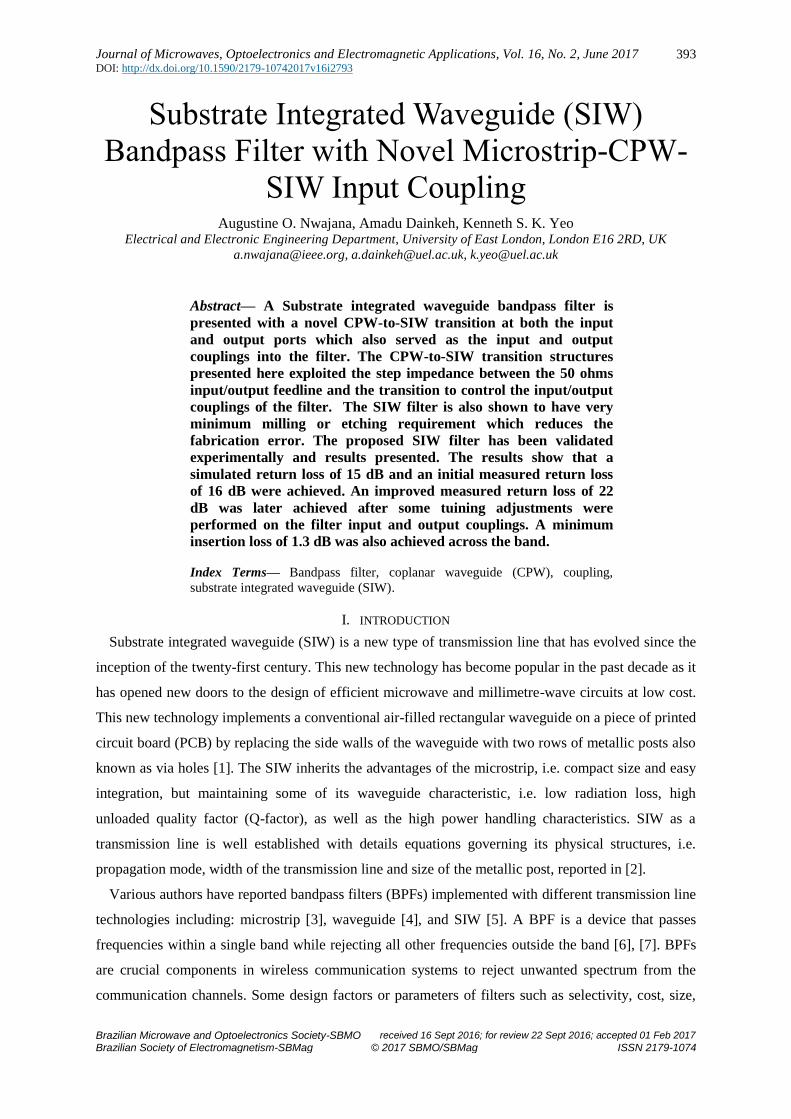
The complete FEM layout of the SIW BPF that was simulated using the Keysight EMPro 3D
simulator is shown in Fig. 6, with all the physical dimensions for the filter shown in Table 2. The
simulation responses of the proposed filter are presented in Fig. 7. It could be seen from the
simulation results that the center frequency of the filter is about 1.68 GHz as designed. A simulated
minimum insertion loss (S21) at the passband of 1.3 dB was achieved. The simulated return loss (S11)
is better than 14.6 dB across the passband. The filter passband is based on the fractional bandwidth
specification and can be controlled by the input/output coupling and the couplings between each pair
of SIW cavities. According to [17], [18]; the distance between neighbouring metal vias p should be
made equal or less than double the diameter of the metal via d (i.e. p ≤ 2d) for best results. The larger
the values of p and b, the higher the electromagnetic leakage through the vias. This means higher
radiation losses which negatively affect the filter insertion and return losses. The radiation loss
becomes negligible at p = 2d as explained in [17].
TABLE II. PHYSICAL DIMENSIONS OF THE SIW BANDPASS FILTER
Fig. 6. Substrate integrated waveguide bandpass filter layout with dimensions.
Dimension Value [mm] Dimension Value [mm]
x1 8.125 y1 3.9 x2 37.25 y2 0.7 x3 111.75 y3 1.1 d 2.0 y4 37.25 p 3.725 s1 13.05
y1 y2 y3
y2
x1
y1 y2
y2 y3
x1
x3
p d
X2 X2 X2
s1 s1 y4

Journal of Microwaves, Optoelectronics and Electromagnetic Applications, Vol. 16, No. 2, June 2017
DOI: http://dx.doi.org/10.1590/2179-10742017v16i2793
Brazilian Microwave and Optoelectronics Society-SBMO received 16 Sept 2016; for review 22 Sept 2016; accepted 01 Feb 2017
Brazilian Society of Electromagnetism-SBMag © 2017 SBMO/SBMag ISSN 2179-1074
400
Fig. 7. Simulation responses of the substrate integrated waveguide bandpass filter.
V. FABRICATION AND MEASUREMENT
The SIW bandpass filter was fabricated using the same material employed in the FEM simulation.
The fabrication was based on printed circuit board (PCB) micro-milling process using the
“Leiterplatten-Kopierfräsen” (LKPF) Protomat C60. The photograph of the fabricated filter is shown
in Fig. 8. In order to facilitate measurement of the filter, two SMA (Sub-Miniature version A)
connectors were fitted onto the input and output ports as shown. The fabricated filter was measured
using the Agilent Vector Network Analyzer. Fig. 9 shows the measured results indicating that a
minimum insertion loss (S21) of 1.3 dB was achieved at the passband. The minimum simulated and
initial measured return losses (S11) of 15 dB and 16 dB were respectively achieved across the
passband. An improved measured return loss of better than 22 dB across the passband was later
achieved after some tuning adjustments were made at the input/output couplings. The improved return
loss is shown in Fig. 9b. The measurement and simulation results are jointly presented in Fig. 10 for
ease of comparison. It is clear from Fig. 10 that the simulation and the initial measurement results are
in good agreement. The improved measured return loss of 22 dB shown in Fig. 10 was achieved by
tuining the filter input and output couplings, while viewing the responses on a vector network
analyzer. The electrical size of the bandpass filter reported in this paper is 0.21λg x 0.63λg which is
more compact than the waveguide filter reported in [4], but less compact when compared to the
microstrip filter reported in [3]. In general, SIW filters are normally smaller in size when compared to
waveguide filters, but are relatively larger in size when compared to microstrip filters. The return loss
of the filter reported in this paper is slightly better than that reported in page 2569 of [4] where the
measured return loss is about 11 dB, as opposed to the minimum measured return loss of 16 dB
achievd here. The roll-off factor and band rejection of our simulated and measured results are very
steepy and in good agreement when compared to that of the filter presented in [4].

Journal of Microwaves, Optoelectronics and Electromagnetic Applications, Vol. 16, No. 2, June 2017
DOI: http://dx.doi.org/10.1590/2179-10742017v16i2793
Brazilian Microwave and Optoelectronics Society-SBMO received 16 Sept 2016; for review 22 Sept 2016; accepted 01 Feb 2017
Brazilian Society of Electromagnetism-SBMag © 2017 SBMO/SBMag ISSN 2179-1074
401
Fig. 8. Fabricated SIW bandpass filter photograph. (a) Top view. (b) Bottom view.
Fig. 9. Measurement results of the SIW bandpass filter. (a) Without tuning. (b) After tuning.
Fig. 10. Comparison of the simulated and measured results of the filter.
VI. CONCLUSION
A substrate integrated waveguide bandpass filter with a new type of Microstrip-CPW- SIW input
coupling has been presented. The proposed filter has been designed, simulated, manufactured and
(b) (a)
(a)
1.5 1.55 1.6 1.65 1.7 1.75 1.8 1.85 1.9 1.95-50
-45
-40
-35
-30
-25
-20
-15
-10
-5
0
S-P
ara
me
ters
(d
B)
Frequency (GHz)
S11
S21
1.5 1.55 1.6 1.65 1.7 1.75 1.8 1.85 1.9 1.95-50
-45
-40
-35
-30
-25
-20
-15
-10
-5
0
S-P
ara
me
ters
(d
B)
Frequency (GHz)
S11
S21
(b)
Journal of Microwaves, Optoelectronics and Electromagnetic Applications, Vol. 16, No. 2, June 2017
DOI: http://dx.doi.org/10.1590/2179-10742017v16i2793
Brazilian Microwave and Optoelectronics Society-SBMO received 16 Sept 2016; for review 22 Sept 2016; accepted 01 Feb 2017
Brazilian Society of Electromagnetism-SBMag © 2017 SBMO/SBMag ISSN 2179-1074
402
measured. The Microstrip-CPW-SIW transition employed as the input coupling in the design allows
two degrees of freedom in controlling the external Q-factor. Stepping the 50 Ohms feedline
impedance to a lower impedance at the SIW end of the transition makes it easier to realize the
required filter external quality factor, Qext. Changing the impedance at the SIW end of the transition,
changes the Qext. The experimentally verified results show that a minimum insertion loss of 1.3 dB
was achieved across the band. An initial measured minimum return loss of 16 dB was achieved before
any tuning was performed on the input/output ports. With some tuning on the filter input and output
couplings, a slight improvement of return loss was achieved with a measured minimum of 22 dB. The
results presented show that there is a good agreement between the simulated and measured filter
responses. Due to the minimum milling/etching of this particular design, a very good agreement
between simulation and raw experimental results was achieved.
REFERENCES
[1] S. H. Han, X. L. Wang, Y. Fan, Z. Q. Yang, and Z. N. He, “The generalized Chebyshev substrate integrated waveguide
diplexer,” Progress in Electromagnetic Research, vol. 73, pp. 29–38, 2007.
[2] D. Deslandes, and K. Wu, “Accurate modelling, wave mechanisms, and design considerations of a substrate integrated
waveguide’” IEEE Trans. Microw. Theory and Techn., vol. 56, no. 6, pp. 2516–2526, Jun. 2006.
[3] C.-F. Chen, S.-F. Chang, and B.-H. Tseng, “Design of compact microstrip sept-band bandpass filter with flexible
passband allocation,” IEEE Microw. Wireless Compon. Lett., vol. 26, no. 5, pp. 346-348, May 2016.
[4] N. Mohottige, O. Glubokov, U. Jankovic, and D. Budimir, “Ultra compact inline E-plane waveguide bandpass filter
using cross coupling,” IEEE Trans. Microw. Theory and Techn., vol. 64, no. 8, pp. 2561–2571, Aug. 2016.
[5] A. Rhbanou, M. Sabbane, and S. Bri, “Design of K-band substrate integrated waveguide band-pass filter with high
rejection,” J. of Microw., Optoelectronics and Electromagnetic Applications, vol. 14, no. 2, pp. 155-169, Dec. 2015.
[6] A. O. Nwajana and K. S. K. Yeo, “Microwave diplexer purely based on direct synchronous and asynchronous
coupling,” Radioengineering, vol. 25, no. 2, pp. 247–252, Jun. 2016.
[7] A. O. Nwajana and K. S. K. Yeo, “Multi-coupled resonator microwave diplexer with high isolation,” in Proc. 46th Eur.
Microw. Conf., IEEE, Oct. 2016, pp. 1167–1170.
[8] X.-P. Chen and K. Wu, “Substrate integrated waveguide filter: basic design rules and fundamental structure features,”
IEEE Microw. Mag., vol. 15, no. 5, pp. 108–116, Jul. 2014.
[9] M. Bozzi, A. Georgiadis, and K. Wu, “Review of substrate-integrated waveguide circuits and antennas,” IET Microw.,
Antennas & Propagation, vol. 5, no. 8, pp. 909–920, Jun. 2011.
[10] D. Deslandes and K. Wu, “Integrated microstrip and rectangular waveguide in planar form,” IEEE Microw. Wireless
Compon. Lett., vol. 11, no. 2, pp. 68-70, Feb. 2001.
[11] D. Deslandes, “Design equations for tapered microstrip-to-Substrate Integrated Waveguide transitions,” IEEE MTT-S
Int. Microw. Symp. Dig., May. 2010, pp. 704–707.
[12] D. Deslandes and K. Wu, “Integrated transition of coplanar to rectangular waveguides,” IEEE MTT-S Int. Microw.
Symp. Dig., vol. 2, May 2001, pp. 619–622.
[13] D. Deslandes and K. Wu, “Analysis and design of current probe transition from grounded coplanar to substrate
integrated rectangular waveguides,” IEEE Trans. Microw. Theory and Techn., vol. 53, no. 8, pp. 2487–2494, Aug.
2005.
[14] Y. Huang and K. L. Wu, “A broad-band LTCC integrated transition of laminated waveguide to air-filled waveguide for
millimeter-wave applications,” IEEE Trans. Microw. Theory and Techn., vol. 51, no. 5, pp. 1613–1617, May 2003.
[15] L. Xia, R. Xu, B. Yan, J. Li, Y. Guo, and J. Wang, “Broadband transition between air-filled waveguide and substrate
integrated waveguide,” IET Electron. Lett., vol. 42, no. 24, pp. 1403–1405, Nov. 2006.
[16] Y. Ding and K. Wu, “Substrate integrated waveguide-to-microstrip transition in multilayer substrate,” IEEE Trans.
Microw. Theory and Techn., vol. 55, no. 12, pp. 2839–2844, Dec. 2007.
[17] D. Deslandes and K. Wu, “Single-substrate integration technique of planar circuits and waveguide filters,” IEEE Trans.
Microw. Theory and Techn., vol. 51, no. 2, pp. 593–596, Feb. 2003.
[18] J.-S. Hong, Microstrip Filters for RF/Microwave Applications. New York, NY, USA: 2011.
[19] X. Chen, W. Hong, T. Cui, J. Chen, and K. Wu, “Substrate integrated waveguide (SIW) linear phase filter,” IEEE
Microw. Wireless Compon. Lett., vol. 15, no. 11, pp. 787-789, Nov. 2005.
[20] K. S. K. Yeo and A. O. Nwajana, “A novel microstrip dual-band bandpass filter using dual-mode square patch
resonators,” Progress in Electromagnetic Research C, vol. 36, pp. 233–247, 2013.


![A Review of Substrate Integrated Waveguide End-Fire Antennas · Some practical dif˝culties for the development of SIW ... Yagi-Uda antennas, and etc. [2] [4]. ... formances and application](https://static.documents.pub/doc/80x56/5e83e92851a5832de8270049/a-review-of-substrate-integrated-waveguide-end-fire-antennas-some-practical-difculties.jpg)