

Switching Energy in CMOS Logic: How far are we from physical limit?
Saibal MukhopadhyayArijit Raychowdhury
Professor: Kaushik RoyDept. of Electrical & Computer Engineering
Purdue University
Network for Computational Nanotechnology
NRLNRL NANOELECTRONICSNANOELECTRONICSRESEARCH LABRESEARCH LAB

2
Outline• Switching energy in charge transfer based
Digital Logic– Basics and Physical Limits
• Practical consideration for switching energy in CMOS Logic– Static requirements– Dynamic requirements– System considerations
• What can we do to reduce switching energy ?• Summary
3
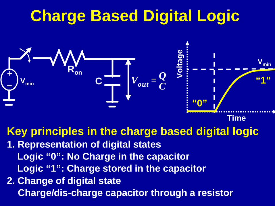
Charge Based Digital Logic
Key principles in the charge based digital logic1. Representation of digital states
Logic “0”: No Charge in the capacitorLogic “1”: Charge stored in the capacitor
2. Change of digital stateCharge/dis-charge capacitor through a resistor
=outQV C
+– C
RonVmin
“0”
“1”
Vmin
Time
Vo
ltag
e

4
Switching Energy
+– C
RonVmin
∞
∞
= = =
= = =
∴ → = − =
∫ ∫
∫ ∫
2min min 0 min0 0
20 0 0 min0 0
2min
( )
1( ) ( )
21
(0 1)2
DD
DD
VTotal DD
VCap C
diss Total Cap
E i t V dt CV dv CV
E i t v t dt Cv dv CV
E E E CV
( )DDi t
=( ) oC
dvi t C
dt
“0”
“1”
Vmin
Time
Vo
ltag
eSwitching energy can be minimized by
reducing Q and/or Vmin
==
2min
min dissE CV
QV
5
Physical Medium for Computation: Barrier Model
Eb
V=Vmin=Ebmin
V=0
Tox
SOURCE DRAIN
Leff
GATE
Vg
Vd

6
Minimum Barrier Height: Zhirnov’s Model
LchEb
( ) 10
~ exp 1ch
err b B b B err
For L nm
P E k T E k Tln P
>
− => =
_ _
_ _ err err cl err QM
err cl err QM
P P P
P P
= +
−
Minimum barrier height = Ebmin ~ kBTln(2)
Channel Length (Lch) [nm]
Min
bar
rier
hei
gh
t (E
b)
in k
BT
Lch=32nm Lgate = 45nm
7
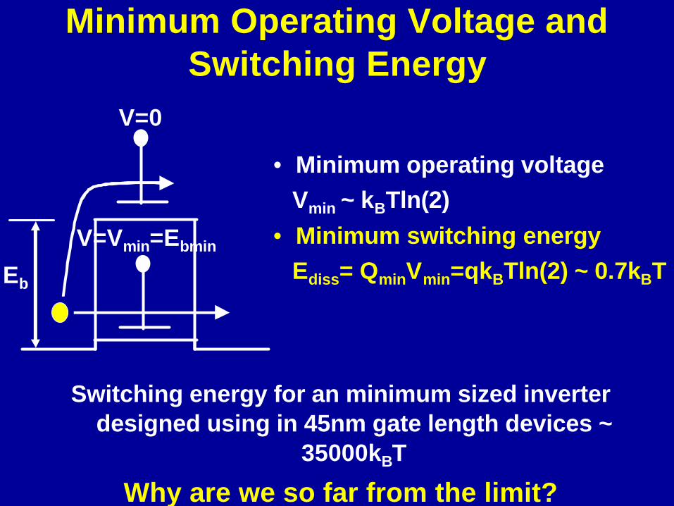
Minimum Operating Voltage and Switching Energy
Eb
V=Vmin=Ebmin
V=0
• Minimum operating voltage Vmin ~ kBTln(2)
• Minimum switching energy Ediss= QminVmin=qkBTln(2) ~ 0.7kBT
Switching energy for an minimum sized inverter designed using in 45nm gate length devices ~
35000kBT
Why are we so far from the limit?
1. Can we operate with Vmin ~ KBTln2 ?
2. Can we operate with Qmin = q ?

9
Outline• Switching energy in charge transfer based
Digital Logic– Basics and Physical Limits
• Practical consideration for switching energy in CMOS Logic– Static requirements– Dynamic requirements– Circuit/System considerations
• What can we do to reduce switching energy ?• Summary
10
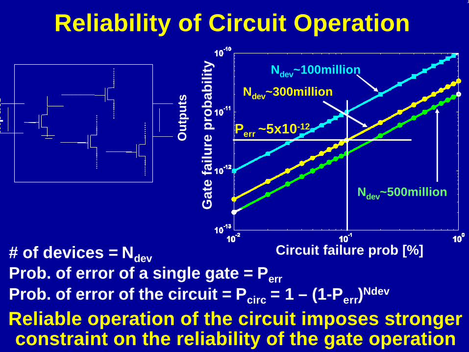
Reliability of Circuit OperationIn
pu
ts
Ou
tpu
ts
# of devices = Ndev
Prob. of error of a single gate = Perr
Prob. of error of the circuit = Pcirc = 1 – (1-Perr)Ndev
Reliable operation of the circuit imposes stronger constraint on the reliability of the gate operation
Circuit failure prob [%]
Gat
e fa
ilure
pro
bab
ility
Perr ~5x10-12
Ndev~100million
Ndev~300million
Ndev~500million

11
Reliable Operation for a Device
• Reliable operation requires a higher barrier– Perr = 0.5
=> Eb= 0.7kBT– Perr = 5x10-12
=> Eb= 25kBT
• 0.1% failure rate for a circuit of 300 million devices => Vmin~25kBT
Eb=25kBT
Perr ~ 5x10-12
Bar
rier
Hei
gh
t in
kBT
Device error probability (Perr)
kBTln(2) 25kBTReliability
Lgate=45nmLch=32nm

12
CMOS Logic: Physical Model
CMOS logic operates based on presence or absence of charge and not on localization of charge
VDD
Vin Vo
“0” ≡ 0V“1” ≡ VDD
“1” ≡ VDD“0” ≡ 0V
VoutVin

13
Operation of MOS Device
V=VDD=EbOFF – EbON
EbON
EbOFF
V=0
onBDD
off
pk TV ln
q pη
=
Operation with a larger pon/poff requires a higher supply voltage
Vg
Csemi
Cox
1 semi oxC Cη = +

14
Operation of CMOS Logic
( )( )( )
0
0
10.5 0.5
1DD BonB B
inoff B
exp q V V k Tpk T k TV ln ln
q p q exp qV k Tη η
− − − = × + × − −
VDD
Vin Vo
VIL VIHVOL
VOH NML = VIL-VOL
NMH = VOH-VIH
Av= Max gain
V in=V
o

15
Operation of CMOS Logic
Higher pon/poff improves maximum gain and noise margin
100on
off
pp
=
10on
off
pp
=
4on
off
pp
=
2on
off
pp
=

16
Operation of CMOS Logic
“1” Vol
“0” Voh
?
2n+1 stages
DD
DD v
2n+1 2n+1DD v
O DD
O
Vin = V 2-
Vo(1) = Vin(2) = V 2 + A
Vo(2n+1) = V 2- (-1)
1, , V V 2
1, , Vv
v OH
A
if A as n
if A as n V
∆
∆
∆
< → ∞ →
> → ∞ →
M
Vin
Vo
ut

17
Operation of CMOS Logic
distinguishability=> Gain (AV) > 1
for CMOS inverterMinimum pon/poff
is “4”and
not “2”
AV=1
pon/poff=4
( )
( ) ( )
2 1
2 2
BDD v
min B
k TV ln A
q
V k T q ln
η= +
=> =
Vmin= kBTln(2) Vmin= 2kBTln(2)Device to Inverter
18
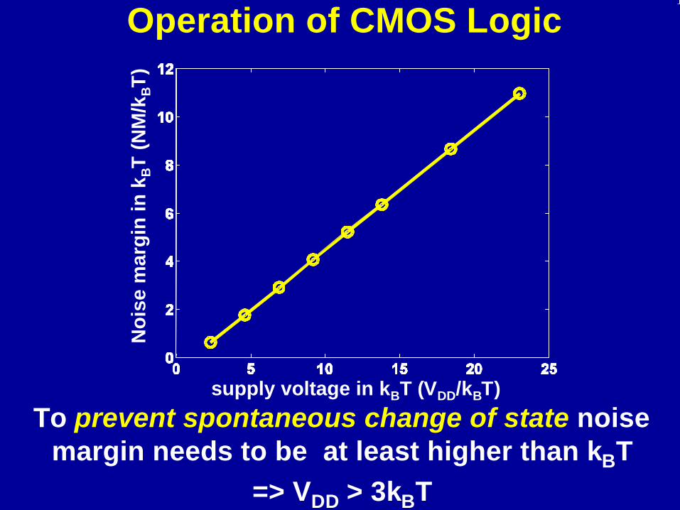
Operation of CMOS Logic
To prevent spontaneous change of state noise margin needs to be at least higher than kBT
=> VDD > 3kBT
supply voltage in kBT (VDD/kBT)
No
ise
mar
gin
in k
BT
(NM
/kBT
)

19
Reliability of Circuit OperationIn
pu
ts
Ou
tpu
ts
# of gates = Ngate
Prob. of error of a single gate = Perr
Prob. of error of the circuit = Pcirc = 1 – (1-Perr)Ndev
Reliable operation of the circuit imposes stronger constraint on the reliability of the gate operation
Circuit failure prob [%]
Gat
e fa
ilure
pro
bab
ility
Perr ~5x10-12
Ngate~100million
Ngate~300million
Ngate~500million

20
Std. dev of noise voltage [mV]
No
ise
Mar
gin
in k
BT
Perr~5x10-12
Perr~5x10⁻¹⁰
Perr~5x10⁻⁸
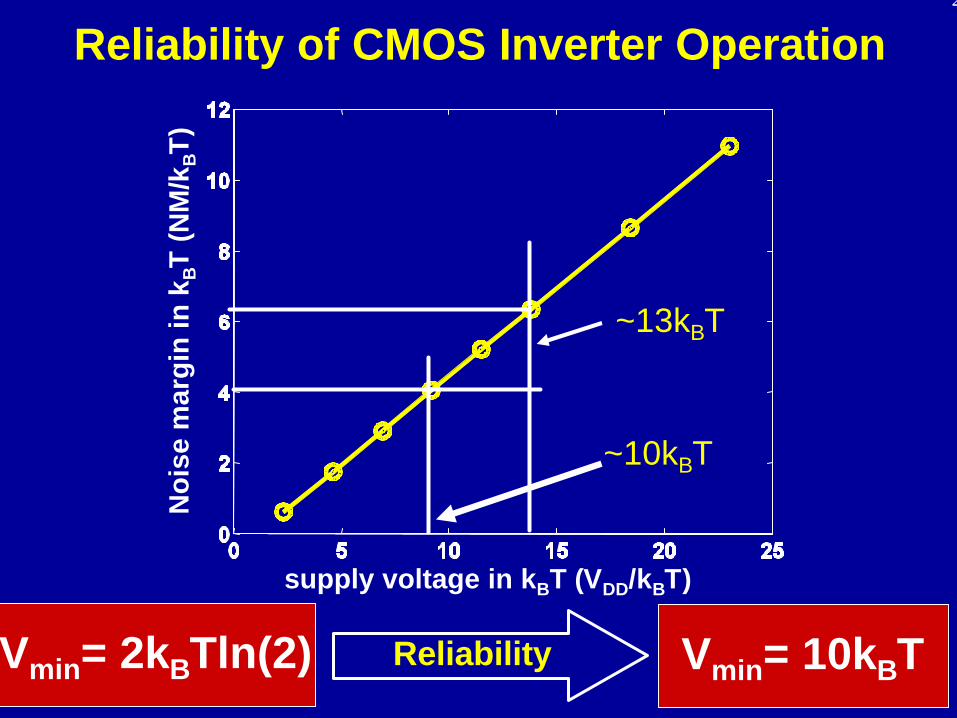
Reliability of CMOS Inverter Operation
NMNM
σN
Vnoise
Higher noise requires a larger noise margin for reliable operation
21
supply voltage in kBT (VDD/kBT)
No
ise
mar
gin
in k
BT
(NM
/kBT
)
~10kBT
~13kBT
Reliability of CMOS Inverter Operation
Vmin= 2kBTln(2) Vmin= 10kBTReliability
Operations of CMOS Logic
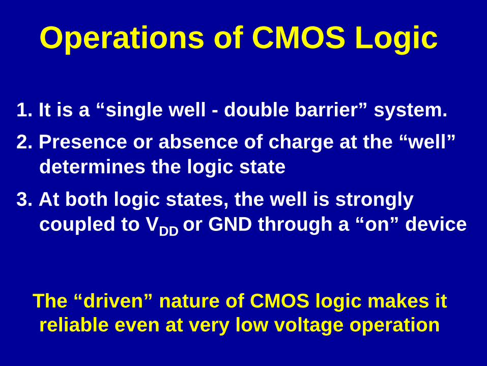
1. It is a “single well - double barrier” system.
2. Presence or absence of charge at the “well”determines the logic state
3. At both logic states, the well is strongly coupled to VDD or GND through a “on” device
The “driven” nature of CMOS logic makes it reliable even at very low voltage operation
23
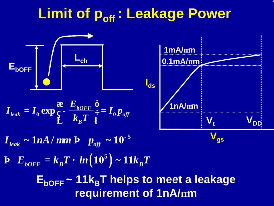
Limit of poff : Leakage Power
EbOFF ~ 11kBT helps to meet a leakage requirement of 1nA/µm
LchEbOFF
0 0exp bOFFleak off
B
EI I I p
k T
= − =
1mA/µm0.1mA/µm
1nA/µm
Vgs
Vt VDD
Ids
( )5
5
~ 1 / ~ 10
10 ~ 11
leak off
bOFF B B
I nA m p
E k T ln k T
µ −⇒
⇒ = ×

24
Outline• Switching energy in charge transfer based
Digital Logic– Basics and Physical Limits
• Practical consideration for switching energy in CMOS Logic– Static requirements– Dynamic requirements– Circuit/System considerations
• What can we do to reduce switching energy ?• Summary

25
Delay in CMOS Logic
+– C
RonVmin
VDD
Vin Vo
“0”
“1”
Vmin
Time
Vo
ltag
e
“0”
“1”
Vmin
Time
Vo
ltag
e

26
Delay and Switching Energy
• Delay through an RC circuit– Independent of applied voltage Vmin
– Lower C reduces both delay and switching energy : key principle in technology scaling
+– C
RonVmin
“0”
“1”
Vmin
Time
Vo
ltag
e
~RonC

27
Delay and Switching Energy : CMOS Logic
The dependence of Ron
on the applied gate bias makes delay and energy
correlated for CMOS
Vg
C
Ron
gmVgs
2
2eff
: 2 2
1 3 2
gate DD on
P N min
par min bOFFmin ox DD ox DD
ox min
C V I
For W W L
C L EL C V C V
C L q
τ
τµ η
=
= =
+ = −

28
Impact of Delay on Minimum VDD
Cpar ~ 30% x Cgate
No parasitics
µneff ~ 300 cm2 / V-sec
Delay Target [ps]
Su
pp
ly V
olt
age
in k
BT
Vmin= 10kBT Vmin= 28kBTDelay (1ps)
29
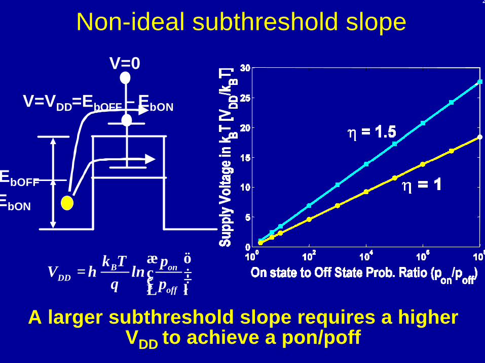
Non-ideal subthreshold slope
V=VDD=EbOFF – EbON
EbON
EbOFF
V=0
onBDD
off
pk TV ln
q pη
=
A larger subthreshold slope requires a higher VDD to achieve a pon/poff

30
Non-ideal subthreshold slope
Non-ideal subthreshold slope increases the VDD required to achieve a certain delay
η=1.5
η=1.0
Vgs
VDD
Ids
Delay Target [ps]
Su
pp
ly v
olt
age
in k
BT
[ps]
37kBT
31
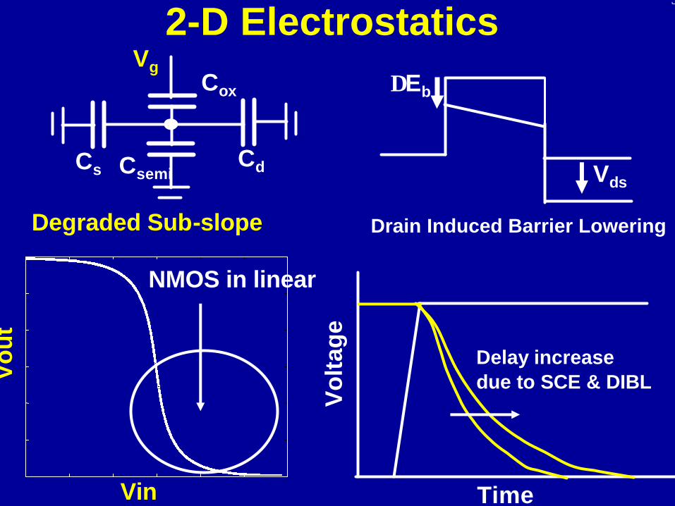
2-D Electrostatics
Drain Induced Barrier Lowering
Vds
∆Eb
CdCsemiCs
Cox
Vg
Degraded Sub-slope
Time
Vo
ltag
e
Vin
Vo
ut
NMOS in linear
Delay increasedue to SCE & DIBL

32
Under same leakage power 2-D effect increases the VDD required to achieve a target delay
2-D Electrostatics
Barrier Lowering (mV)
VD
D re
qu
ired
fo
r τ
= 1p
s
VDD ~ 39kBT

33
Process Variability
• Leakage ~ poff variation• Reliability ~ pon/poff variation• Delay ~ variation in EbOFF will change the delay
Variation in Process Parameters
Vds
∆Eb
The designed EbOFF and VDD needs to be increased to account for the effect of variation
± 10% variation in EbOFF => VDD ~ 42kBT
Vgs
VDD
Ids
34
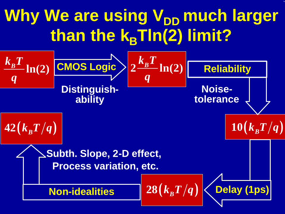
Why We are using VDD much larger than the kBTln(2) limit?
ln(2)Bk Tq
CMOS Logic
Distinguish-ability
2 ln(2)Bk Tq
Reliability
Noise-tolerance
( )10 Bk T q
Delay (1ps)( )28 Bk T q
( )42 Bk T q
Non-idealities
Subth. Slope, 2-D effect, Process variation, etc.

35
Drivability in Digital Logic
Vmin needs to be developed across a finite capacitance for driving the next gate
Vmin Vmin
+– C
Ron
Vmin C
Ron
C C
Vmin“0”
“1”
“0” Vmin
“1”
“0” Vmin “0”
“0”Vmin “0”

36
Drivability and Minimum Charge
Drivability requirement does not allow to operate with a single electron for CMOS logic operation
Load Capacitance [F]
Nu
mb
er o
f el
ectr
on
s
min size NMOS ~260
min size INV ~ 800
FO4 (w/ par) + local interconnect ~5300min minQ CV=
Lgate=45nmLch=32nm
Vmin~ 42k BT
Vmin~ 2k B
Tln(2)

37
Drivability and Switching Energy
Capacitance [F]
Sw
itchi
ng e
nerg
y in
kBT
min size NMOS ~11000
Vmin~ 42k BT
Vmin~ 2kBTln(2)
min size INV ~ 33000
FO4 (w/ par) + local interconnect ~ 220,000
Drivability requirement increases the minimum switching energy for an inverter to ~ 33,000 kBT
Lgate=45nmLch=32nm

Switching Energy in CMOS Logic Delay ~ 1ps, High reliability
kBTln(2) 42kBTDelay/Reliability
33000kBT
Drivability

39
Outline• Switching energy in charge transfer based
Digital Logic– Basics and Physical Limits
• Practical consideration for switching energy in CMOS Logic– Static requirements– Dynamic requirements– Circuit/System considerations
• What can we do to reduce switching energy ?• Summary

40
Operation of CMOS Circuits
• For logic operation a gate has to drive more than one gates in a CMOS logic
• Typical fanout is assumed to be 4
F/F F/F
C 4C

Switching Energy in CMOS Logic Delay ~ 1ps, High reliability
kBTln(2) 42kBTDelay/Reliability
220,000kBT
Drivability
33000kBTFO4

42
Switching Energy for a System
Driving “long” interconnects can significantly increase the switching energy
280,000
2,800,000
28,000,000
Capacitance [F]
Sw
itch
ing
En
erg
y in
kBT
43
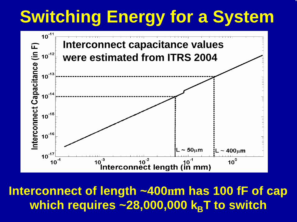
Interconnect of length ~400µm has 100 fF of cap which requires ~28,000,000 kBT to switch
Switching Energy for a SystemInterconnect capacitance values were estimated from ITRS 2004
44
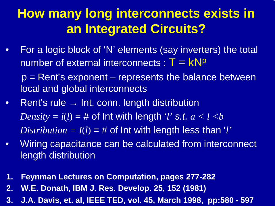
How many long interconnects exists in an Integrated Circuits?
• For a logic block of ‘N’ elements (say inverters) the total number of external interconnects : T = kNp
p = Rent’s exponent – represents the balance between local and global interconnects
• Rent’s rule → Int. conn. length distribution Density = i(l) = # of Int with length ‘l’ s.t. a < l <bDistribution = I(l) = # of Int with length less than ‘l’
• Wiring capacitance can be calculated from interconnect length distribution
1. Feynman Lectures on Computation, pages 277-282 2. W.E. Donath, IBM J. Res. Develop. 25, 152 (1981)3. J.A. Davis, et. al, IEEE TED, vol. 45, March 1998, pp:580 - 597
45
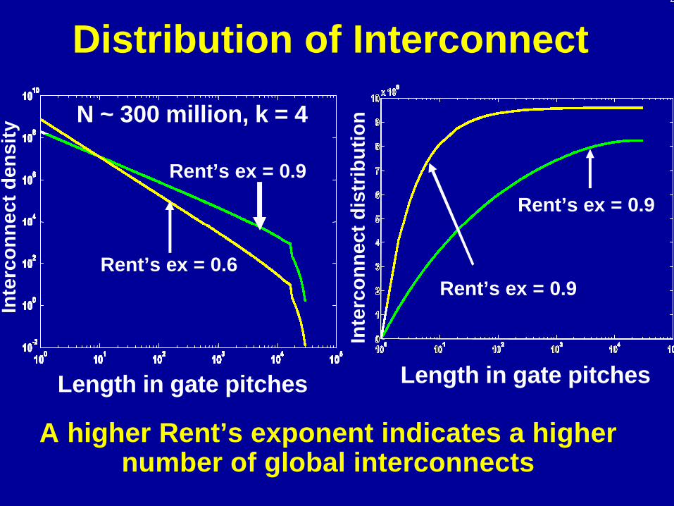
A higher Rent’s exponent indicates a higher number of global interconnects
Distribution of Interconnect
Length in gate pitchesLength in gate pitches
Inte
rco
nn
ect
den
sity
Inte
rco
nn
ect
dis
trib
uti
on
Rent’s ex = 0.9
Rent’s ex = 0.6Rent’s ex = 0.9
Rent’s ex = 0.9
N ~ 300 million, k = 4
46
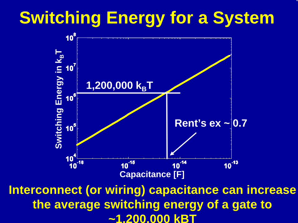
Switching Energy for a System
1,200,000 kBT
Capacitance [F]
Sw
itch
ing
En
erg
y in
kBT
Rent’s ex ~ 0.7
Interconnect (or wiring) capacitance can increase the average switching energy of a gate to
~1,200,000 kBT

Practical Limits in Switching Energy in CMOS Systems
Physical Limit: kBTln(2)
Requirement for Computation: 33,000 kBTReliability, Speed and Drivability
Requirement for Communication: 1,200,000 kBT
Local and global communication

48
How can we reduce the practical switching energy limit?

49
Switching Energy and Leakage Power Trade-off
Cpar ~ 0.3 x COX, η=1.5Delay target ~ 1ps
Leakage Current [nA/µm]
VD
Dre
qu
ired
in k
BT
Operating at 10X higher leakage can reduce the switching energy from 33,000kBT to 23,000 kBT
Vgs
VDD
Ids
Target Ioff
50
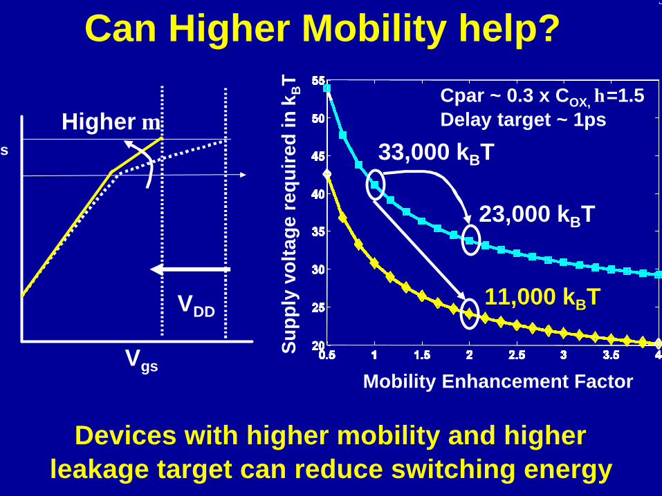
Devices with higher mobility and higher leakage target can reduce switching energy
Can Higher Mobility help?
23,000 kBT
11,000 kBT
33,000 kBT
Vgs
VDD
Ids
Higher µ
Mobility Enhancement Factor
Su
pp
ly v
olt
age
req
uir
ed in
kBT
Cpar ~ 0.3 x COX, η=1.5Delay target ~ 1ps

51
Switching Energy and Delay Trade-off
pon=1
pon < 1
Delay Target [ps]
Su
pp
ly V
olt
age
in k
BT
For delay targets > 100ps subthreshold operation is more energy efficient
Reliability req.

52
Rent’s Exponent
Int.
conn
. cap
per
gat
e [f
F]
# o
f in
terc
on
nec
ts
Switching Energy for a System
230,000 kBT
1,200,000 kBT
Reducing the number of local interconnects can significantly reduce the system switching energy

53
Single Electron Operation in CMOS
Load Capacitance [F]
Nu
mb
er o
f el
ectr
on
s
min minQ CV=
V min~ 42k B
T
Vmin~ 2k B
Tln(2)
Single electron operation at room temperature is only possible if C < 9aF

54
Single electron operation in CMOS logic is possible for L < 8nm
Scaling and Single Electron Operation in CMOS
Min
imum
# o
f ele
ctro
ns
Channel Length [nm]
Lch~ 8nm
Vmin ~ 2kBT ln (2)
Vmin ~ 42kBT
EOT ~ 1.8nm

55
Scaling helps to reduce switching energy even if the supply voltage remains the same
Scaling and Switching Energy

56
Scaling and Thermal Noise
Increase in thermal noise at lower capacitance can reduce the energy benefit of scaling
+– C
Ron
4 4
: 0.1 12
: 9 43
B Bnoise noise
noise
noise
k TR k TV
RC CFor C fF mV
For C aF mV
σ
σ
σ
= = =
= => =
= => =

57
1. Can we operate with Vmin ~ KBTln2 ?• Reliability• Delay• sub. slope, 2-D effects, variability etc.
2. Can we operate with Qmin = q ?• Drivability• Parasitic and Interconnect capacitance
Summary
Device/Circuit/System level investigations can reduce the practical limit of switching energy, but it is very difficult to achieve the physical
limit in CMOS logic

58
References
1. V. Zhirnov et. al, Proceedings of the IEEE, vol. 91, Nov 2003 pp. 1934 – 1939.
2. J. D. Meindl, Proceedings of the IEEE, Vol.83, April 1995, pp.:619 - 635
3. W.E. Donath, IBM J. Res. Develop. 25, 152 (1981)4. J.A. Davis, et. al, IEEE TED, vol. 45, March 1998,
pp:580 – 597 (two consecutive papers)5. L. B. Kish, Phys. Lett. A, vol. 305, pp. 144–149, 2002.6. Y. Taur and T. H. Ning, Fundamentals of Modern VLSI
Devices, Cambridge University Press, 1998

59
Questions and Answers

60
Single electron operation in CMOS logic is possible for L < 8nm
Scaling and Single Electron Operation in CMOS
Min
imum
# o
f ele
ctro
ns
Channel Length [nm]
Lch~ 8nm
Vmin ~ 2kBT ln (2)
Vmin ~ 42kBT
EOT ~ 1.8nm

61
Drivability in Digital Logic
Vmin needs to be developed across a finite capacitance for driving the next gate
Vmin Vmin
+– C
Ron
Vmin C
Ron
C C
Vmin“0”
“1”
“0” Vmin
“1”
“0” Vmin “0”
“0”Vmin “0”

62
Drivability and Minimum Charge
Drivability requirement does not allow to operate with a single electron for CMOS logic operation
Load Capacitance [F]
Nu
mb
er o
f el
ectr
on
s
min size NMOS ~260
min size INV ~ 800
FO4 (w/ par) + local interconnect ~5300min minQ CV=
Lgate=45nmLch=32nm
Vmin~ 42k BT
Vmin~ 2k B
Tln(2)


