
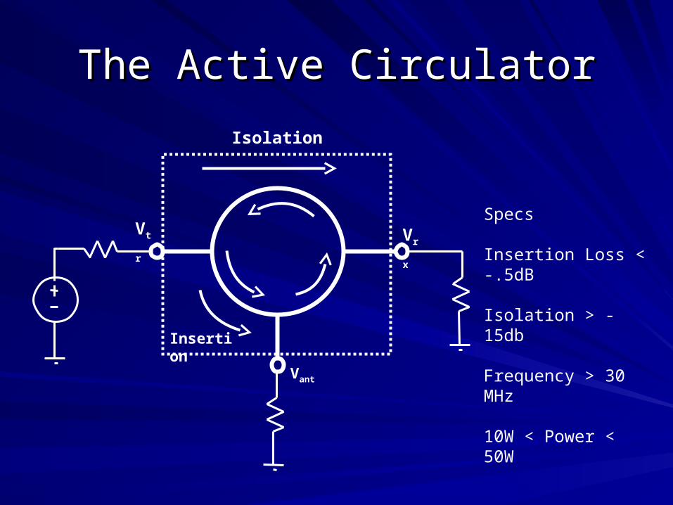
The Active CirculatorThe Active Circulator
Insertion
Vtr
Isolation
Vant
Vrx
Specs
Insertion Loss < -.5dB
Isolation > -15db
Frequency > 30 MHz
10W < Power < 50W
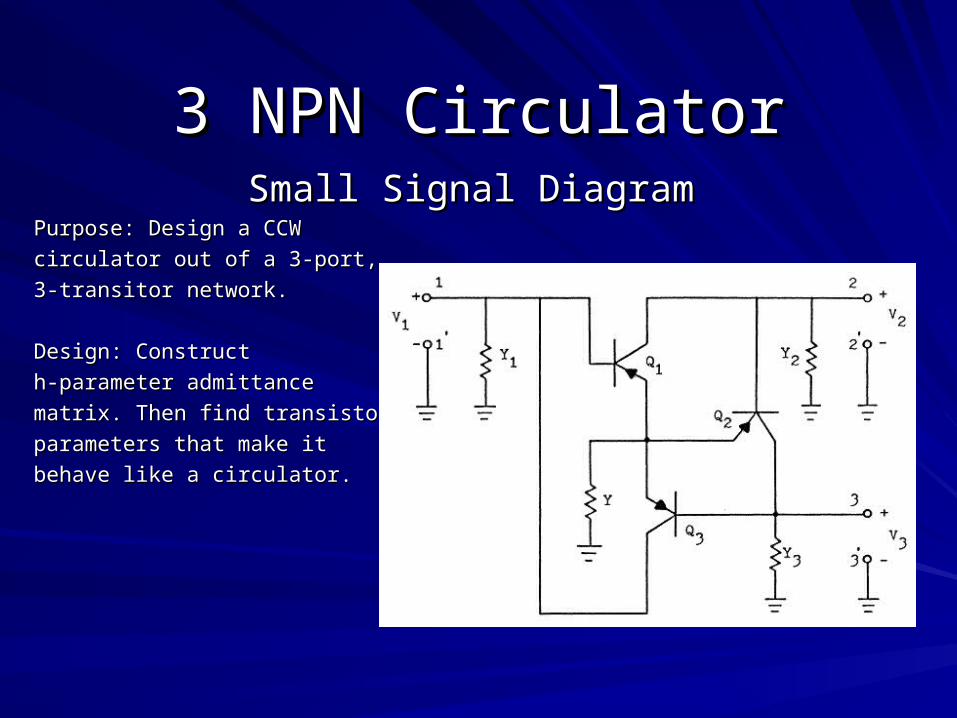
3 NPN Circulator3 NPN CirculatorSmall Signal DiagramSmall Signal Diagram
Purpose: Design a CCW Purpose: Design a CCW
circulator out of a 3-port, circulator out of a 3-port,
3-transitor network.3-transitor network.
Design: Construct Design: Construct
h-parameter admittanceh-parameter admittance
matrix. Then find transistormatrix. Then find transistor
parameters that make it parameters that make it
behave like a circulator.behave like a circulator.

Tanaka-Lee SchematicTanaka-Lee Schematic

Experiment ResultsExperiment ResultsOperating Points: VOperating Points: Vtrs trs = 100mV, f = 1kHz= 100mV, f = 1kHz
Results: Isolation = -19.33dB, Insertion Loss = -1.012dB Results: Isolation = -19.33dB, Insertion Loss = -1.012dB
Power = 1.13mWPower = 1.13mW

SimulationSimulation

ConsiderationsConsiderations
Cons:Cons:
Bias CurrentBias Current
VVbebe Overdrive Overdrive
RRpipi Sensitivity Sensitivity
Pros:Pros:
High FrequencyHigh Frequency
Parameters Easily CalculatedParameters Easily Calculated
Symmetric Symmetric

Basic ModelBasic ModelPurpose: A more “flexible” op-ampPurpose: A more “flexible” op-amp
Design Specs:Design Specs:
V1=V2=7.5VV1=V2=7.5V
V3=-0.8VV3=-0.8V
IR1=IR2=1mAIR1=IR2=1mA

3-Port Scheme 3-Port Scheme
Idea from the topology in the proposalIdea from the topology in the proposal

Continued: Simulation ResultContinued: Simulation Result
Insertion Loss: -1.41DB
Need simplification for analysis purpose.

Simplified TopologySimplified Topology

Continued-Simulation ResultContinued-Simulation Result

Continued-Small Signal Test Continued-Small Signal Test
Signal From the Transmitter (f_input=1kHz)Signal From the Transmitter (f_input=1kHz)
Vtransmitter=49.60mVVtransmitter=49.60mV
Vantenna=25.2mVVantenna=25.2mV
Vreceiver=1.84mvVreceiver=1.84mv
F(-3db)=298.7kHzF(-3db)=298.7kHz
Insertion Loss=-6DB Isolation Loss=-31.50DBInsertion Loss=-6DB Isolation Loss=-31.50DB
Signal From the Receiver (f_input=1kHz)Signal From the Receiver (f_input=1kHz)
Vantenna=49.8mVVantenna=49.8mV
Vreceiver=43mvVreceiver=43mv
Vtransmitter=0mVVtransmitter=0mV
F(-3db)=805.3kHzF(-3db)=805.3kHz
Insertion Loss=-1.27DB Isolation Loss=-InfInsertion Loss=-1.27DB Isolation Loss=-Inf
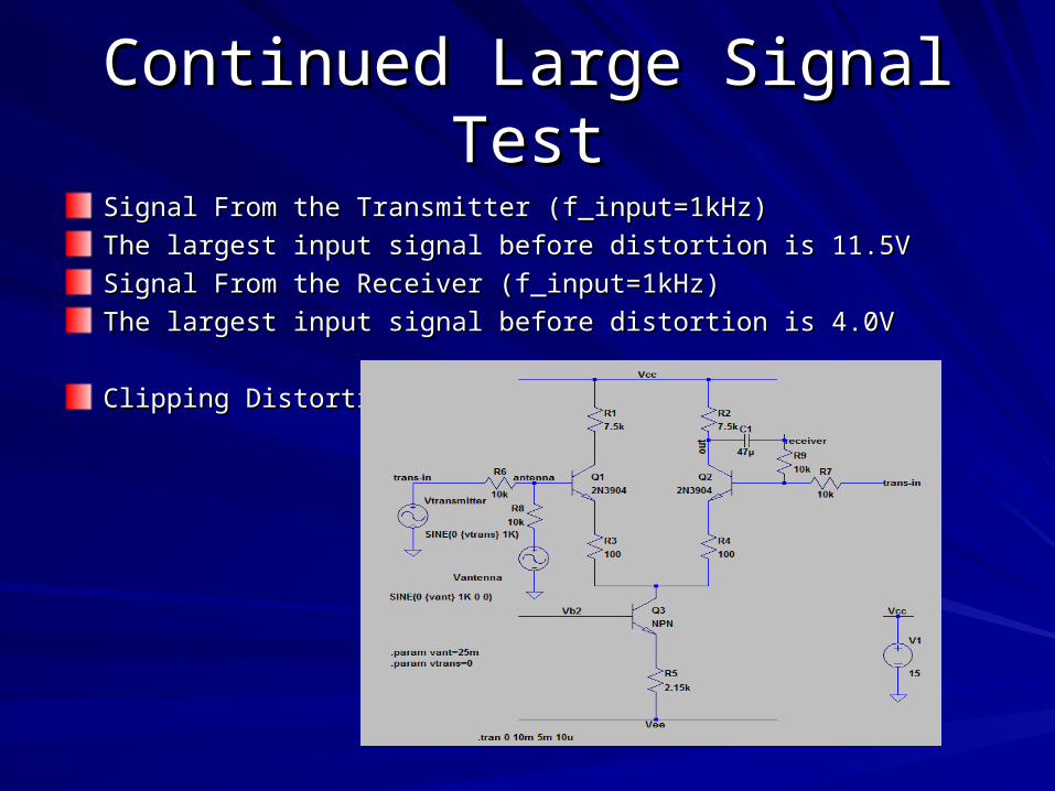
Continued Large Signal TestContinued Large Signal Test
Signal From the Transmitter (f_input=1kHz)Signal From the Transmitter (f_input=1kHz)
The largest input signal before distortion is 11.5VThe largest input signal before distortion is 11.5V
Signal From the Receiver (f_input=1kHz)Signal From the Receiver (f_input=1kHz)
The largest input signal before distortion is 4.0VThe largest input signal before distortion is 4.0V
Clipping DistortionsClipping Distortions

Continued-BandwidthContinued-Bandwidth
Vantenna 50mV 500mV 1V 4V
-3DB Voltage 35.4mV 353.56mV 0.707V 2.828V
Bandwidth(KHz) 871.5 805.4 757.2 1.32

Basic Model3-Port, Symmetric, Op-Amp
Topology
Purpose:Purpose:To understand the limiting factors involved with Op-Ampsused in this topology
Method:Method:Push the limits of readily available LM741 Op-Amps, to betterunderstand the capability of this topology.

Testing ResultsSmall Signal Test:Small Signal Test:
RRoo: 11k V: 11k VBIASBIAS: +/- 20 DC : +/- 20 DC
VVtrtr : 250mV : 250mVpppp V Vantant(-3dB) occurred at 180 kHz (-3dB) occurred at 180 kHz
Large Signal Test:Large Signal Test:
RRoo: 11k V: 11k VBIASBIAS: +/- 20 DC : +/- 20 DC
VVtrtr : 17V : 17Vpppp V Vantant(-3dB) never occurred, clipping(-3dB) never occurred, clipping
Clipping occurred at 8kHz, yielding calculated slew rate of .427 V/usClipping occurred at 8kHz, yielding calculated slew rate of .427 V/us
Isolation:Isolation:
Ideal operating condition, 1 VIdeal operating condition, 1 Vpppp @ 1 kHz : -23.7 dB @ 1 kHz : -23.7 dB
Small Signal max frequency: -10.17 dBSmall Signal max frequency: -10.17 dB
Large Signal max frequency: -29.19 dB Large Signal max frequency: -29.19 dB

Alternative Model
This model was determined to be too finicky with resistance mismatching. Far too much distortion was found in the experiments, and the topology was abandoned
QuickTime™ and a decompressor
are needed to see this picture.
The input was a sinusoid…

Topology Modeled for our purpose, not a true circulator

Simulation Results
Testing ResultsSmall Signal Test:Small Signal Test:
RRoo: 11k V: 11k VBIASBIAS: +/- 20 DC : +/- 20 DC
VVtrtr : 200mV : 200mVpppp V Vantant(-3dB) occurred at 224 kHz (-3dB) occurred at 224 kHz
Large Signal Test: Large Signal Test:
RRoo: 11k V: 11k VBIASBIAS: +/- 20 DC : +/- 20 DC
VVtrtr : 1V : 1Vpppp V Vantant(-3dB) occurred at 200kHz(-3dB) occurred at 200kHz
•Dr. Young mentioned frequency should be our focus, not power, Dr. Young mentioned frequency should be our focus, not power,
hence, the significantly smaller large signal voltage.hence, the significantly smaller large signal voltage.
Isolation:Isolation:
Ideal operating condition, 1 VIdeal operating condition, 1 Vpppp @ 1 kHz : -25.03 dB @ 1 kHz : -25.03 dB
Small Signal max frequency: -29.05 dBSmall Signal max frequency: -29.05 dB
Large Signal max frequency: -49.11 dB Large Signal max frequency: -49.11 dB
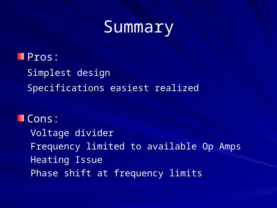
Summary
Pros:
Simplest design
Specifications easiest realized
Cons:Voltage divider
Frequency limited to available Op Amps
Heating Issue
Phase shift at frequency limits

ConclusionConclusion
There are many paths we can take.There are many paths we can take.
Pursue high power: Op/Diff amp designPursue high power: Op/Diff amp design
Pursue high frequency: 3 transistorPursue high frequency: 3 transistor
Pursue a compromise…Pursue a compromise…
We recommend the Op/Diff amp design We recommend the Op/Diff amp design because it is the most realizable.because it is the most realizable.

Questions?Questions?


