
The Design of Asynchronous Memory Management Unit
Chris Myers Alain Martin Computer System Lab. CS Dept. Stanford University Cal. Tech
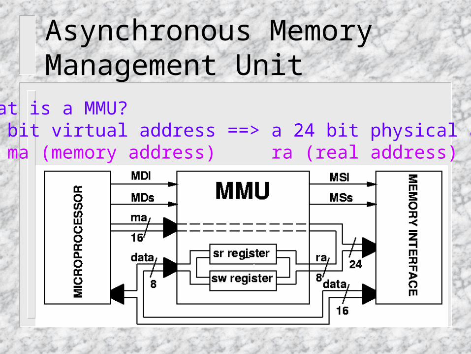
Asynchronous Memory Management Unit• What is a MMU? 16 bit virtual address ==> a 24 bit physical address. ma (memory address) ra (real address)

Memory Management Unit
16 bit virtual address + 8-bit segmentation register ==> a 24 bit physical address. sr: Segementation Read register (FFFF) sw: Segementation Write register (FFFE)
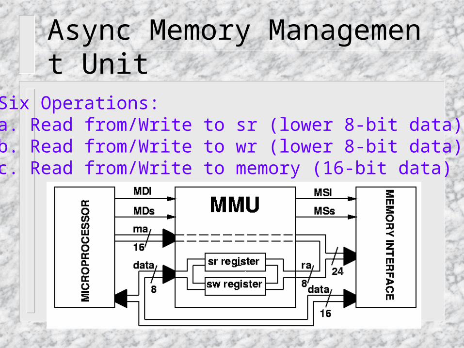
Async Memory Management Unit• Six Operations: a. Read from/Write to sr (lower 8-bit data) b. Read from/Write to wr (lower 8-bit data) c. Read from/Write to memory (16-bit data)
Async Memory Management Unit
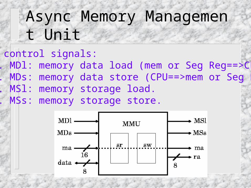
• 4 control signals: a. MDl: memory data load (mem or Seg Reg==>CPU) b. MDs: memory data store (CPU==>mem or Seg Reg) c. MSl: memory storage load. d. MSs: memory storage store.
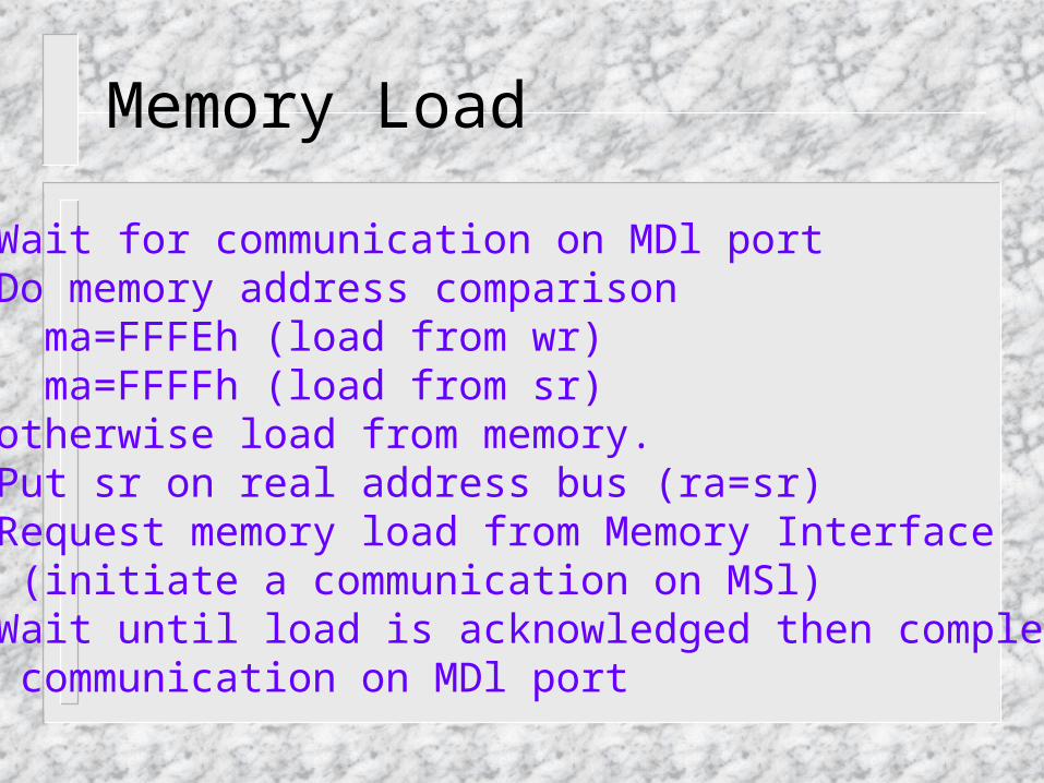
Memory Load
• Wait for communication on MDl port • Do memory address comparison ma=FFFEh (load from wr) ma=FFFFh (load from sr) otherwise load from memory.• Put sr on real address bus (ra=sr) • Request memory load from Memory Interface (initiate a communication on MSl)• Wait until load is acknowledged then complete communication on MDl port

Store Seg. Read Register
• Wait for communication on MDs port • Do memory address comparison check ma=FFFFh • Put value from data bus into the sr register • Complete communication on MDs port

Design Flow

CSP Specification of MMU
MDs]]MSs;sw;:rab3 []
MDsdata;:swb2 []
MDsdata;:srb1 [
FFFE));(maFFFF)(maFFFE),(maFFFF),(ma
:b3b2,(b1,MDs[ []
MDl]MSl;sr;:rab3 []
MDlsw;:datab2 []
MDlsr;:datab1 [
FFFE));(maFFFF)(maFFFE),(maFFFF),(ma
:b3b2,(b1,MDl[[*
Load
Store
load from sr register
load from sw register
load from memory
write to sr registerwrite to sw register
write to memory
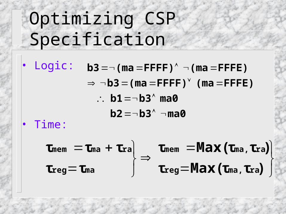
Optimizing CSP Specification
• Logic:
• Time:ma0b3b2
ma0b3b1
FFFE)(maFFFF)(mab3
FFFE)(maFFFF)(mab3
)τMax(ττ
)τMax(ττ
ττ
τττ
rama,reg
rama,mem
mareg
ramamem

Optimizing CSP Specification
MDs]]MSs;b3 []
MDsdata;:swb2 []
MDsdata;:srb1 [
ma0));b3ma0,b3b2b1,
FFFE);(maFFFF)(ma:(b3||sw):((raMDs[ []
MDl]MSl;b3 []
MDlsw;:datab2 []
MDlsr;:datab1 [
ma0));b3ma0,b3b2b1,
FFFE);(maFFFF)(ma:(b3||sr):((raMDl[[*

Process Decomposition
• Control path:

Process Decomposition
• Datapath: A. comparator:
B. Registers:
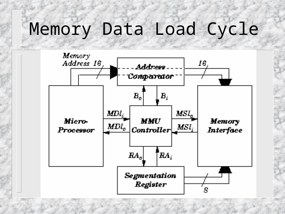
Memory Data Load Cycle
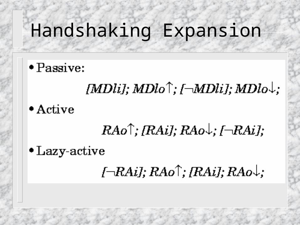
Handshaking Expansion

Handshaking Expansion

Handshaking Expansion

Handshaking Expansion

Handshaking Expansion
• Reshuffling
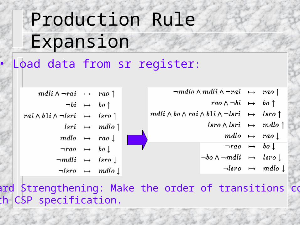
Production Rule Expansion
• Load data from sr register:
Guard Strengthening: Make the order of transitions confirmwith CSP specification.

PR Implementation

Handshaking Expansion:datapath
• Datapath:
• Reshuffling:

PR Implementation: datapath
• PADIN: single-rail memory address =>
dual-rail memory address

PR Implementation: datapath
• determines if bits ma15-ma1 are all high.

PR Implementation: datapath
• determines if bits ma15-ma1 are all high.


