
November-December 2010November-December 2010Volume 14, Number 6Volume 14, Number 6
The International Magazine for the Semiconductor Packaging IndustryThe International Magazine for the Semiconductor Packaging Industry
Wafer-Level TestDesign for ReliabilityFine-Pitch Copper Wire BondingStress Analysis for 3D Wafer ThinningInternational Directory of Wire Bonders
Wafer-Level TestDesign for ReliabilityFine-Pitch Copper Wire BondingStress Analysis for 3D Wafer ThinningInternational Directory of Wire Bonders
Chip Scale Review. Nov/Dec 2010. [ChipScaleReview.com] 1
CONTENTS
Nov-Dec 2010 Volume 14, Number 6
The International Magazine for Device and Wafer-level Test, Assembly, and Packaging
Addressing High-density Interconnection of Microelectronic IC's including 3D packages, MEMS,
MOEMS, RF/Wireless, Optoelectronic and Other Wafer-fabricated Devices for the 21st Century.
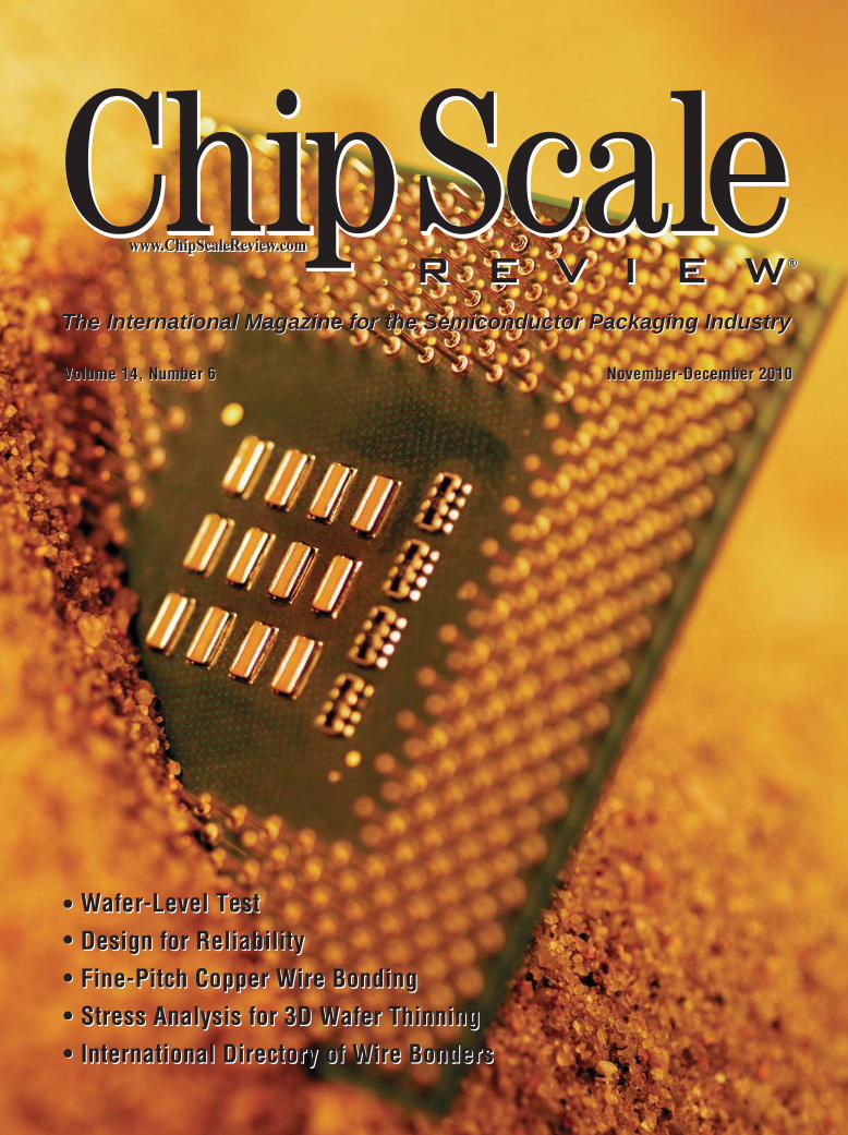
Cover photo rights reserved Chip Scale Review
This edition’s cover dramatically depicts sand or silica
(aka: silicon dioxide) as the raw material for transformation to
a silicon wafer. This process is achieved through many steps
including the Czochralski process and eventually results
as this flip-chip ball grid array. During the manufacturing
cycle a number of sequential processes occur to achieve
this final step. In this edition of CSR we have assembled a
rich set of in-depth articles that unravel a few areas of these
complex transforming processes that range from TSV silicon
interposers, wafer test/probing and the increasing adoption
of copper wire bonding, the criticality of emphasis for
design and test reliability and the significant challenges
of ultra-low alpha emitting solder materials.
FEATURE ARTICLES
Stress Analysis of Wafer Thinning Processes for 3D-ICJames Hermanowski and Sumant Sood, SUSS MicroTec, Inc.
Scott Sullivan, Disco Corp., Hans-Dieter Geiler and Kristian Schulz, JenaWave GmbH
3D Glass and Silicon Interposers: A $950M Business by 2015Jean-Marc Yannou, Yole Développement
Fine Pitch Copper Wire BondingHorst Clauberg, Ivy Qin, Paul Reid and Bob Chylak
Kulicke and Soffa Industries, Inc.
Probabilistic Design for Reliability (PDfR)Ephraim Suhir, ERS Company
University of California Santa Cruz, University of Maryland College Park
Challenges in Supply of Ultra-low Alpha Emitting Solder MaterialsAndy Mackie, PhD, Indium Corporation, Olivier Lauzeral, iROC Technologies
14
18
20
24
29
Chip Scale Review. Nov/Dec 2010. [ChipScaleReview.com] 5
From the Publisher World Series Champions . . . The , a Perfect Example of Teamwork!
Kim Newman, Chip Scale Review
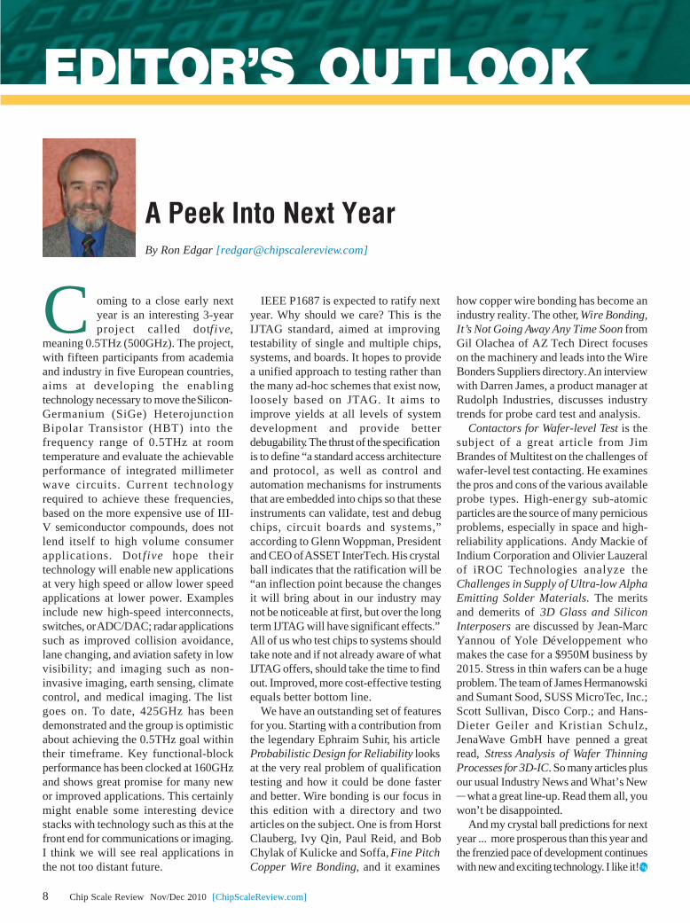
Editor's Outlook A Peek Into Next Year
Ron Edgar, Technical Editor, Chip Scale Review
Industry News IWLPC 2010 in Review
Chip Scale Review Staff
Interview Probing Questions for Rudolph Technologies
Françoise von Trapp, Contributing Editor
2010 International Directory of Wire Bond Equipment ManufacturersRon Molnar, Az Tech Direct, LLC
What's New!, Product Showcase
Advertiser Index, Advertising Sales
CONTENTS
FEATURE ARTICLES
DEPARTMENTS
32
38
6
8
10, 42
12
36
46
48
Wire Bonding . . . It's Not Going Away Any Time SoonGil Olachea, AZ Tech Direct, LLC
Contactors for Wafer-level TestJim Brandes, Multitest
Copyright © 2010 High Connection Density, Inc. All rights reserved. Information is subject to change without notice. “SuperSpring” and “SuperButton” are trademarks of High Connection Density, Inc.
820A Kifer Road, Sunnyvale, CA 94086 (408) 743-9700 x331
www.hcdcorp.com [email protected]
ISO 9001:2000 Certi�ied
Our Proprietary Technology Your Competitive Advantage
SuperButton® SuperSpring®
Featuring HCD Patented SuperButton® and
SuperSpring® Contact Elements incorporated into
socket and interposer solutions for prototyping, validation, space transformer, and test
applications.
Stop by and learn more about our innovative connector
technology at these upcoming shows:
IMAPS 2010November 2-4
Booth 818
Silicon Valley Test Conference November 8-9
SuSuuuupepepppppepppp rBrBBrBBBrBBBBButuuuuuu totototoooooon®nn®n®nnnnnn BeBeeBeeeee tstsstsssstst iiinnnnnnn CClClClCCCC asasasasasasasss s ssss elelllllllececececececceececctrtrtrtttt icicicicicciccalalalaaalaa
pppepepepppepppepepp rfrfffffffffffffororrororororrorooo maamaamaaaaaaaancnnnnnnn e ee aaananananaanaaa d dd d ccoocococcocoocooooooontntnttttttacacacacacacacacaacaccct tt rereeeeererelllilililillilililiiiababbbbbbbililililiililillilililititii yyyyyy
Chip Scale Review. Nov/Dec 2010. [ChipScaleReview.com]6
World Series Champions . . .
The , a Perfect Example of Teamwork !
FRFRFRFRFROM OM OM OM OM THE PUBLISHERTHE PUBLISHERTHE PUBLISHERTHE PUBLISHERTHE PUBLISHER
STAFF
Kim Newman [email protected] Michaels Managing [email protected] Edgar Technical [email protected]çoise von Trapp Contributing [email protected] Winkler Contributing [email protected]. Tom Di Stefano Contributing [email protected] M. Sakamoto Contributing Editor [email protected] Mirabito Contributing Legal [email protected] Peters Contributing Legal [email protected]
SUBSCRIPTION--INQUIRIES
Chip Scale ReviewT 408-429-8585F [email protected]
Advertising Production Inquiries:Kim [email protected]
EDITORIAL ADVISORS
Dr. Thomas Di Stefano Centipede SystemsRon Molnar Az Tech Direct, LLC.Dr. Andy Mackie Indium Corp. of AmericaDr. Thorsten Teutsch Pac Tech USACharles Harper Technology SeminarsDr. Guna Selvaduray San Jose State UniversityProf. C.P. Wong Georgia TechDr. Ephraim Suhir ERS CompanyNick Leonardi Premier Semiconductor Services
Copyright © 2010 by Gene Selven & Associates Inc.
Chip Scale Review (ISSN 1526-1344) is a registered trademark of
Gene Selven & Associates Inc. All rights reserved.
Subscriptions in the U.S. are available without charge to qualified
individuals in the electronics industry. Subscriptions outside of the
U.S. (6 issues) by airmail are $85 per year to Canada or $95 per
year to other countries. In the U.S. subscriptions by first class mail
are $75 per year.
Chip Scale Review, (ISSN 1526-1344), is published six times a
year with issues in January-February, March-April, May-June, July-
August, September-October and November-December. Periodical
postage paid at Los Angeles, Calif., and additional offices.
POSTMASTER: Send address changes to Chip Scale Review
magazine, P.O. Box 9522, San Jose, CA 95157-0522
Printed in the United States
The International Magazine for Device and Wafer-levelTest, Assembly, and Packaging Addressing
High-density Interconnection of Microelectronic IC'sincluding 3D packages, MEMS, MOEMS, RF/Wireless, Optoelectronic and Other Wafer-
fabricated Devices for the 21st Century.
VOLUME 14, NUMBER 6
Kim NewmanPublisher
I actually had my publisher’s letter finished ahead of schedule, but then the SanFrancisco Giants did the unexpected, they won the 2010 World Series! Ever
since I can recall, as the daughter of now retired CSR publisher, Gene Selven, therewas publishing and baseball. My years watching this sport, and specifically cheeringon our hometown favorite Giants, gave me little indication that this seemingly wishfulthought for “the Team” would become a reality.
This is historical, at least as far as everyone in this baseball and publishing familyis concerned, calling for the immediate and unquestionable need to rethink thepublisher’s letter for this issue.
Many days and discussions later, amateurs and enthusiasts alike seem to agree onone key point. The Giants won the Championship because they simply performed asa team. This seems to come as a surprise in the era of teams with highly-paid superstars,when it is actually the main premise of team sports, with each player expected tocontribute equally to win the championship.
Baseball and publishing . . . I have also relied on the teamwork approach to buildmomentum and success. With this approach in mind, I would like to share our teamline-up for 2011, which will lead to another banner year for Chip Scale Review.
Articles, editorials and the supplier directories will continue to be the focus, attractingthe widening base of subscribers and advertisers alike. The successful InternationalWafer-Level Packaging Conference (IWLPC), held in October in partnership with theSMTA Organization, will be enhanced in 2011 with the addition of editorial advisorsto expand the technical content. Show dates for the 2011 event are set for October 3-6, 2011 once again in Santa Clara, California.
Chip Scale Review has been selected official media sponsor for the IEEE/ECTC2011 event and continuing as the BiTS workshop official media sponsor. CSR willalso continue ongoing media sponsorships for SEMICON, MEPTEC and SMTAConferences. Join the CSR Team, as it is never too late to get on the roster for 2011with your article or advertisement, by contacting our staff. Of course, a bigCongratulations to the Giants!
Chip Scale Review. Nov/Dec 2010. [ChipScaleReview.com]8
EDITOR'S OUTLOOK
oming to a close early nextyear is an interesting 3-yearproject called dotf ive,
meaning 0.5THz (500GHz). The project,with fifteen participants from academiaand industry in five European countries,aims at developing the enablingtechnology necessary to move the Silicon-Germanium (SiGe) HeterojunctionBipolar Transistor (HBT) into thefrequency range of 0.5THz at roomtemperature and evaluate the achievableperformance of integrated millimeterwave circuits. Current technologyrequired to achieve these frequencies,based on the more expensive use of III-V semiconductor compounds, does notlend itself to high volume consumerapplications. Dot f ive hope theirtechnology will enable new applicationsat very high speed or allow lower speedapplications at lower power. Examplesinclude new high-speed interconnects,switches, or ADC/DAC; radar applicationssuch as improved collision avoidance,lane changing, and aviation safety in lowvisibility; and imaging such as non-invasive imaging, earth sensing, climatecontrol, and medical imaging. The listgoes on. To date, 425GHz has beendemonstrated and the group is optimisticabout achieving the 0.5THz goal withintheir timeframe. Key functional-blockperformance has been clocked at 160GHzand shows great promise for many newor improved applications. This certainlymight enable some interesting devicestacks with technology such as this at thefront end for communications or imaging.I think we will see real applications inthe not too distant future.
A Peek Into Next YearBy Ron Edgar [[email protected]]
C IEEE P1687 is expected to ratify nextyear. Why should we care? This is theIJTAG standard, aimed at improvingtestability of single and multiple chips,systems, and boards. It hopes to providea unified approach to testing rather thanthe many ad-hoc schemes that exist now,loosely based on JTAG. It aims toimprove yields at all levels of systemdevelopment and provide betterdebugability. The thrust of the specificationis to define “a standard access architectureand protocol, as well as control andautomation mechanisms for instrumentsthat are embedded into chips so that theseinstruments can validate, test and debugchips, circuit boards and systems,”according to Glenn Woppman, Presidentand CEO of ASSET InterTech. His crystalball indicates that the ratification will be“an inflection point because the changesit will bring about in our industry maynot be noticeable at first, but over the longterm IJTAG will have significant effects.”All of us who test chips to systems shouldtake note and if not already aware of whatIJTAG offers, should take the time to findout. Improved, more cost-effective testingequals better bottom line.
We have an outstanding set of featuresfor you. Starting with a contribution fromthe legendary Ephraim Suhir, his articleProbabilistic Design for Reliability looksat the very real problem of qualificationtesting and how it could be done fasterand better. Wire bonding is our focus inthis edition with a directory and twoarticles on the subject. One is from HorstClauberg, Ivy Qin, Paul Reid, and BobChylak of Kulicke and Soffa, Fine PitchCopper Wire Bonding, and it examines
how copper wire bonding has become anindustry reality. The other, Wire Bonding,It’s Not Going Away Any Time Soon fromGil Olachea of AZ Tech Direct focuseson the machinery and leads into the WireBonders Suppliers directory. An interviewwith Darren James, a product manager atRudolph Industries, discusses industrytrends for probe card test and analysis.
Contactors for Wafer-level Test is thesubject of a great article from JimBrandes of Multitest on the challenges ofwafer-level test contacting. He examinesthe pros and cons of the various availableprobe types. High-energy sub-atomicparticles are the source of many perniciousproblems, especially in space and high-reliability applications. Andy Mackie ofIndium Corporation and Olivier Lauzeralof iROC Technologies analyze theChallenges in Supply of Ultra-low AlphaEmitting Solder Materials. The meritsand demerits of 3D Glass and SiliconInterposers are discussed by Jean-MarcYannou of Yole Développement whomakes the case for a $950M business by2015. Stress in thin wafers can be a hugeproblem. The team of James Hermanowskiand Sumant Sood, SUSS MicroTec, Inc.;Scott Sullivan, Disco Corp.; and Hans-Dieter Geiler and Kristian Schulz,JenaWave GmbH have penned a greatread, Stress Analysis of Wafer ThinningProcesses for 3D-IC. So many articles plusour usual Industry News and What’s New_ what a great line-up. Read them all, youwon’t be disappointed.
And my crystal ball predictions for nextyear ... more prosperous than this year andthe frenzied pace of development continueswith new and exciting technology. I like it!
Chip Scale Review. Nov/Dec 2010. [ChipScaleReview.com]10
INDUSTRY NEWS
T his year’s 7th annual IWLPC,held October 11-14 in SantaClara CA, set out to connect thefuture of wafer-level-packaging,
3D, and MEMS with an agenda featuringmore than 50 presentations from experts ineach area, a marketing panel discussion, asupply chain panel discussion, and akeynote and kick off that tied the wholething together. The successful event reportedlyboasted an increased attendance of 10% withinternational representation from 13 countries.
European 3D PlatformOpening speaker Peter Ramm,
Fraunhofer EMFT, set the stage with apresentation on “The European 3DTechnology Platform for HeterogeneousSystems” on Tuesday evening. The 3Dprogram he leads focuses on heterogeneoussystems and stacking devices containingMEMS systems. Ramm’s presentationfeatured Fraunhofer’s definitions of various3D configurations. He explained that thechoice of 3D technology depends on cost-effectiveness, performance requirements andavailability of devices. While through siliconvia (TSV) technology is considered one ofthe most promising, high-performance, andsmall formfactor 3D technologies today,CMOS Image Sensors (CIS) are the onlyproduct on the market using 3D TSVtechnology. According to Ramm, fabricationof heterogeneous systems often shows theneed for post-back-end-of-line (BEOL) 3Dintegration and mixed approaches.
Among the current projects Ramm’s team
IWLPC 2010 in ReviewChip Scale Review Staff
is working on is the recently launchedeBRAINS, which stands for European BestReliable Ambient Intelligent NanosensorSystems. This EU commission-fundedconsortium picks up where its predecessor,e-Cubes, left off. The latter focused ondeveloping wireless sensor technologyintegrating ICs, ultra- mini MEMS devices,RF, power, memory etc. eBRAIN will focuson improving the reliability of the microand nano systems themselves. Ramm saidsince the September 1 launch, he’s veryhappy with the way things are progressing.
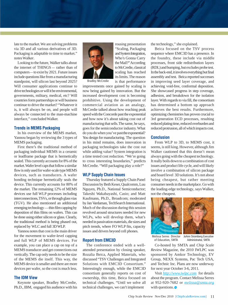
Marketing PanelWe d n e s d a y ’s
Marketing PanelDiscussion featuredthree well-respectedindustry forecasters:Jim Walker, Dataquest/Gartner Group, Jan
Vardaman, TechSearch International, andJean-Marc Yannou, Yole Développement.Terry Davis, Amkor Technology, moderatedthe discussion.
WLP is PervasiveIn her presentation, Vardaman remarked
Jim Walker Jan Vardaman
Jean-Marc Yannou
that WLP is pervasive throughout ourindustry and increasing over time. Shereported a current capacity shortage for300mm WLPs, but expects that to bealleviated by the end of the year as capitalexpenditures are expected for additionalcapacity of both 200mm and 300mmbefore then. While the majority ofdemand for WLPs is still driven by themobile phone market, Vardaman notesother applications are responsible as well.For example, the Apple iPad, of which2.3M per month are being shipped.
The star of the WLP show is fan-out WLP(FO WLP) and more specifically Infineon’seWLB technology. Vardaman reports thatSTATS ChipPAC has shipped 35M eWLBpackages and more versions of FO WLPcan be expected soon including from othermanufactures driven by wireless applications.ASE has licensed eWLP; Nepes bought theRCP line from Freescale and is developinga 3D SiP solution; and Infineon is workingto develop a PoP version in its next-generation eWLB.
Solving Problems via 3DWalker noted that the convergence of
bandwidth and speed, design cost andcomplexity, and time-to-market is drivingthe 3D packaging market. He said thatsilicon integration methods take too long,and that packaging is becoming theintegrator. “We’re lagging Moore’s Law. It’staking too long. Design starts are slowingdown with regards to advanced featuresizes. There’s revenue to be lost by being
Chip Scale Review. Nov/Dec 2010. [ChipScaleReview.com] 11
late to the market. We are solving problemsvia 3D and all various derivatives of 3D.Packaging is adaptable to time to market.”notes Walker.
Looking to the future, Walker talks aboutthe internet of THINGS _ rather than ofcomputers _ to exist by 2021. Future issuesinclude questions like from a manufacturingstandpoint, will silicon last beyond 2025?Will consumer applications continue todrive technologies or will it be environmental,governments, military, medical, etc? Willcountries form partnerships or will businesscontinue to drive the market? “Whatever itis, it will always be on, and people willalways be connected to the man-machineinterface,” concluded Walker.
Trends in MEMS PackagingIn his overview of the MEMS market,
Yannou began by reviewing the 3 types ofMEMS packaging.
First there’s the traditional method ofpackaging individual MEMS in a ceramicor leadframe package that is hermeticallysealed. This currently accounts for 8% of themarket. Wafer level caps that follow a similarflow is only used for wafer-scale type MEMSdevices, such as transducers. A waferbonding technique hermetically seals thedevice. This currently accounts for 80% ofthe market. The remaining 12% of MEMSdevices use full WLP processes includinginterconnections, TSVs, or through glass vias(TGV). He also mentioned an additionalemerging technology _ thin film capping bydeposition of thin films on wafers. This canbe done using either silicon or glass. Clearly,the traditional method is being phased out,replaced by WLC and full 3D WLP.
Yannou notes that cost is the main driverfor the movement to wafer-level cappingand full WLP of MEMS devices. Forexample, you can place a cap on top of aMEMS transducer and get connections outvertically. The cap only needs to be the sizeof the MEMS die itself. This way, theMEMS device is smaller and there are moredevices per wafer, so the cost is much less.
The IDM ViewKeynote speaker, Bradley McCredie,
Ph.D., IBM, engaged his audience with his
rousing presentation“Scaling, Packagingand System Integration,Who’s Gonna Carrythe Mail?” Accordingto McCredie, classicalscaling has reachedits limits. The reasonis that performance
improvements once gained by scaling isnow being gained by innovation. But theincreased development cost is becomingprohibitive. Using the development ofcommercial aviation as an analogy,McCredie talked about how reaching peakspeed with the Concorde past the exponentialand how now it’s about taking cost out ofmanufacturing that sells. The same, he says,goes for the semiconductor industry. Whatdo you do when you’ve past the exponential?You design for manufacturing. The questionin his mind remains, does innovation inpackaging technologies take the cost outwhile adding value? System integration isa time tested cost reduction. “We’re goingto cross interesting boundaries,” predictsMcCredie. “Will packaging play a role?”
WLP Supply Chain IssuesThursday featured a Supply Chain Panel
Discussion by Beth Keser, Qualcomm, LuuNguyen, Ph.D., National Semiconductor;Takeshi Wakabayashi, Casio; and MattKaufmann, Ph.D., Broadcom; moderatedby Jan Vardaman, TechSearch International.Much of the discussion during this sessionrevolved around structures needed for newWLPs, who will develop them, what’sneeded in passivation materials, die sizes andpitch trends, where FO WLP fits, capacityissues and drivers beyond cell phones.
Report from EMC3DThe conference ended with a well-
attended presentation by closing speaker,Rozalia Beica, Applied Materials, whodiscussed “TSV Challenges and IntegratedSolutions with EMC3D Consortium.”Interestingly enough, while the EMC3Dconsortium generally reports on cost ofownership, this time, Beica focused ontechnical challenges. “Until we solve alltechnical challenges, we can’t implement
Bradley McCredie
the technology,” she explained.Beica focused on the TSV process
sequence where EMC3D has a presence. Inthe foundry, these include via middleprocesses, front side redistribution layers(RDL) and bumping, but excludes probe test.In the back-end, it involves everything but finalassembly and test. Beica reported successesin improving seed layer coverage, andachieving void-free, conformal deposition.She showcased progress in step coverage,adhesion, and breakdown for the isolationlayer. With regards to via fill, the consortiumhas determined a bottom up approachachieves the best results. Furthermore,optimizing chemistries has proven crucial to3rd generation ECD processes, resultingreduced plating time, reduced overburden andreduced protrusion, all of which impacts cost.
ConclusionFrom WLP to 3D, to MEMS cost, it
seems, is still king. However, although JimWalker cautioned that this doesn’t meanalways going with the cheapest technology.It really boils down to a combination of costissues and product life cycle, and will likelyinvolve a combination of silicon packageand board level 3D solutions. It’s not aboutbeing cheapest, but rather meetingconsumer needs in the marketplace. Go withthe leading-edge technology, says Walker,not the cheapest.
Co-hosted by SMTA and Chip ScaleReview Magazine, the 2010 IWLPC wassponsored by Amkor Technology, EVGroup, NEXX Systems, Pac Tech USA,and Technic Inc. Plans are now underwayfor next year October 3-6, 2011.
Visit http://www.iwlpc.com for detailsabout the program. Contact Melissa Serresat 952-920-7682 or [email protected] questions.
Melissa Serres Directorof Education, SMTA
JoAnn Stromberg ExecutiveAdministrator, SMTA
Chip Scale Review. Nov/Dec 2010. [ChipScaleReview.com]12
Probing Questions for Rudolph Technologies
CSR: Thanks for speaking with us today, Darren. To get started,could you talk a bit about the product suite that Rudolph offersfor probe card test & analysis?
DJ : Rudolph offers several different types of probe cardanalyzers for testing the whole gamut of probe cards includinghigh performance cards with high density pins for testing deviceswith a higher number of bond pads that require smaller pitchesand smaller probe tips. One-touch memory applications is onearea of specialty. The PrecisionWoRx System can be easilyconfigured for a variety of probe card technologies.The ProbeWoRx300 System is designed for test and analysisof high speed, high force, and high throughput for high pin-count probe cards and features one-touch scan of all probes.The WaferWoRxs tool for probe process analysis measuresprobe marks.The industry buzz word right now is “known good die (KGD),”but to get that, you have to start with a known good tester andknown good probe card. We provide the mechanism forvalidating the probe card and probing process, to make sureyou have a known good product flow.
CSR: Could you describe the technologies Rudolph uses toevaluate probe cards and how they differ from competingtechnologies?
DJ: Well, there are a couple of different technologies out there.When you’re testing probe cards, you need to do an optical testto make sure the needles are in the correct position and locatedin the right place on the wafer. That’s the first part of the test.The second part is to validate the electrical connections fromPCB all the way down to needles. In some cases, you have toactivate components on the card to establish that it’s a known-good card.
INTERVIEW
By Françoise von Trapp, Contributing Editor
Darren James, Product Manager,Probe Card Test & Analysis (PCTA),Rudolph Technologies, Inc. talks withChip Scale Review about industrytrends for probe card test and analy-sis, and Rudolph’s approach for ad-dressing these.
Optics are used for inspecting needles. Rudolph uses a stage-based approach, camera and optic block, measuring the needlein the free-hanging state. It also performs over-travel to measurethe needles in the working condition. The center of the scrub istargeted because you want to align the needle so it is notscrubbing off the pad.Rather than taking a step-and-repeat approach, our opticalcomparative metrology (OCM) measures the whole surface bymoving the camera underneath. It’s a faster, more appropriateprocess for memory probe cards, where pin counts are movingabove 40-50,000 needles. In this case, we use a fixed reference_ a fiducial plate _ to measure the needle location in X, Y, andZ with a single image scan. This fiducial plate allows us tomeasure a full 300mm array using a continuous scanning motionfor maximum throughput.Our competitors are using step-and-repeat for all technologies,which is considerably slower on larger array cards andsusceptible to more inaccuracies because step-and-repeatmeasures the needle’s X-Y position relative to stage position,whereas OCM measures relative to the fixed reference gridpattern. Rudolph’s patented 3D OCM distinguishes us from ourcompetitors.
CSR: What are the current economic drivers for probe cardtest & analysis?
DJ: Probe cards are becoming more of a whole system as morecomponents are being put on the card. In the final test industry,you’re testing tomorrow’s technology with yesterday’stechnology, which is always a challenge. To expand capabilityof the testers, more circuits are being added to the probe card.What drives all probe card analysis is making sure you have aknown good probe card; touching down in the right place andmaking good contact. However, as the industry moves to multidie, scaling to larger and larger needles, it’s difficult to put allthose under a microscope manually. You need a tool that willdo it for you.
CSR: You talk about Rudolph’s technologies performing bothprobe mark inspection & probe mark analysis. What’s thedifference?
DJ: Probe mark inspection is a “go, no-go” check that isperformed as an all-surface inspection just on the wafer.Basically, it ensures contacts stay within the bond pads. It’s an
Chip Scale Review. Nov/Dec 2010. [ChipScaleReview.com] 13
outgoing quality assurance check used by manufacturers to makesure they have good product going out. Was the mark in thebond pad? If those criteria are met, it’s good to go.Alternatively, probe mark analysis goes beyond inspectionto analyze the process and give feedback, giving the end useran opportunity to go back and fix problems. It’s a much morein-depth process. At Rudolph, our WaferWoRxs analysisengine can be used on NSX tools, and provides more analysisof the scrub marks and how they relate to each other. Itscans across the whole wafer and looks for trends likedeflection issues.
CSR: What kinds of testing process problems can probe markanalysis uncover or provide insight into?
DJ: With inspection, you see that the mark is off the pad, andthe analysis provides the reason why. Then you can makechanges to the process to make sure you’re putting out goodproduct. Until now, the probing process hasn’t had much focusbecause bond pads were large relative to the needle. All thosethings have changed. Pads are getting smaller and needles aregetting smaller and have circuitry underneath, which contributesto the need for control processes that didn’t exist before. It’s allabout process control.Probe mark analysis takes the probe card and evaluates how itworks in the whole system; how it interfaces with the tester.Without this, you can model some of the behavior but until youactually try and implement it, you don’t know how it behaves.Now you can see how it really behaves and where it came from.
CSR: What is ‘predictive scrub’ and how can it be used toimprove probe card performance?
DJ: Predictive scrub is a way to improve the whole process. Ifyou look at the whole system, there’s a lot of interaction goingon. It’s hard to dial in on that if you focus on the individualpieces. While predictive scrub can’t mimic exactly what’shappening in the test cell, what we can do is look at what weexpected the results to be from the analyzer and then look atthe scrub marks to see what actually happened. Then we workbackwards and compensate for that, making improvements tothe process along the way.
CSR: How are increases in sophistication, complexity and costof packaging affecting your business?
DJ: Technology moving forward has helped our business grow.20 years ago there weren’t any analyzers, it was all donemanually. But as technology reaches 40 and 60μm pitch betweenneedles, it’s tough for an operator to align. Other methods are
needed to ensure its being done right and that means tools thatmeasure, monitor, and track. That creates more opportunity.Over the last few years, focus on cost has been affecting anumber of things. Technology changes mean a need for higherthroughput, reduced time on the tools, migration of test area,etc. With the advancement of TSVs, there’s a move away frompackaging and package test. Rather, there’s more focus on sortand testing the wafer itself. Historically it was a two stepprocess. Now, the device becomes the package and that drivesmore test into the sort area. Part of this is due to customeroutsourcing, selling bare die or the wafer itself. The end useris only interested in buying KGD. They want assurances thatthe die they put in their cell phone is good because the wholepackage is expensive.In the sort area, new probe cards allow for higher speeds closerto true operational speeds. If you weed out the bad die in thesort area it minimizes the amount, and therefore the overall costof final test.In the 3D integration space Rudolph is doing a lot of inspectionwork, but on the probe card side, we’re still trying tounderstand what changes this will drive. One option is testingon the lower substrate in the stack rather than the package,and testing bond pads on the package, but only time will tellif that’s a viable approach. We’re seeing efforts to reduce theforce that each needle applies, but there’s still a trade-offbetween force and contact; the more force the better the contactresistance. You need to manage all the tradeoffs. We don’thave a really good feel yet for how probing of TSV deviceswill be implemented.
CSR: One final question. What future trends do you see on thehorizon for probe card testing and analysis?
DJ: I see three major trends moving forward. First of allinnovation in tip technologies for probe card needles will allowfor higher densities across the board for DRAM andmicroprocessors, and more needles in a tighter space. On theother extreme, but driving in a similar direction, I see largerscale across the board with multi-die testing, and bigger arrays.The whole probe process therefore becomes more challenging.As the probe array gets bigger, you still have the sameconstraints; you have to control surface planarity. How do wego from a small one-inch area, and while still maintainingprocess, move to a 12” area, all the while increasing force from60-300kg to maintain planarity across a huge area? That’s thechallenge moving forward on how to do that.Additionally, how do we handle the higher temperatures movingforward, for example190-200oC required in medical andautomotive devices? And finally, there will be a trend to reducecost of test and cost of interconnects.
Chip Scale Review. Nov/Dec 2010. [ChipScaleReview.com]14
Stress Analysis of Wafer Thinning Processes for 3D-ICBy James Hermanowski and Sumant Sood [SUSS MicroTec, Inc.], Scott Sullivan [Disco Corp.]Hans-Dieter Geiler and Kristian Schulz [JenaWave GmbH]
W ith growing interconnectdensities and rising costsof IC manufacturing in
leading edge technology nodes, 3Darchitectures for IC integration andpackaging are being adopted by devicemanufacturers. This drive towards 3D ICand stacked chips requires the thinning ofdevice wafers down to 30-120μm. A typical3D-TSV integration process flow involvestemporary wafer bonding of a processeddevice wafer to a supporting carrier waferand subsequent thinning of the device waferto the desired thickness. Cracking andchipping are major yield factors for thinnedwafers. This article examines the stressesinduced as a result of thin wafer processingand discusses a way to measure the stressesusing nondestructive techniques whilemitigating undesired stresses.
To keep a process in control, measurementsmust be taken. One key factor insemiconductor devices is stress. There area number of different methods to measurethe stress of devices and surfaces. Thechallenge is to find a method that measuresthe stress on the device wafer as a whole,while having the resolution to find localizedareas of interest.
In this study, a scanning infrareddepolarization (SIRD) stress measurementtool* is used to measure the stress in a waferas it is processed through edge trimming,bonding, and thinning. The results of thetests show that it is possible to measurewhile processing; thus controlling theamount of stress the device wafer issubjected to during bonding and thinning.
Micro-Raman spectroscopy is a methodwell suited for measuring localized stressin silicon wafers. When setting up a waferthinning process, this destructive testmethod can be used to measure the stressat the grind mark and find the depth of theresultant stress. On occasion, micro-Ramanspectroscopy is used as a process control.Published stress values at the grind marksin silicon are between 25MPa to 175MPa
and the effects being observed are up to10μm deep. Unfortunately, Micro-Ramanspectroscopy does not meet some of thisstudy’s requirement for process monitoring.However, the test method does give a goodbaseline value for stress induced by grinding.
A common non-destructive method formeasuring silicon wafers is X-raydiffraction (XRD). With both reflective andtransmissive functions, surface stress andinternal defects can be measured. Ofparticular interest to this work was one ofthe well-known limitations of XRD.
The stress measurement tool, SIRD,represents a full wafer shear stress imagerbased on an infrared transmissionpolarimeter. A linear, polarized laser beamof 1.3μm wavelength penetrates the wafer,and the emitted light is analyzed by use ofan analyzer of the polarization state (firstStokes component). The optical arrangementis shown in Figure 1. When a wafer isstress-free, the polarization state stays
unchanged during the transition and thedepolarization D is zero. If the wafercontains local or global stress fields, thestress-induced birefringence of the crystalcauses stress-related depolarization. Byscanning the wafer (rotation and translationwith polar coordinates) a map is producedand, taking into account the recordeddepolarization, the shear stress equivalentG is calculated. This dimensionlessequivalent G is proportional to the planarshear stress in polar coordinates. Theproportionality is determined by the piezo-optic wafer module M, including the piezo-optic constants of the material and the waferthickness. Both should be known.
As can be seen by the optical schema ofSIRD, the stress-induced phase-shift effectbetween ordinary and extraordinary beamsis integrated across the wafer thickness(integrated photoelasticity). Hence, there isno information about the stress distributionacross the wafer thickness. From theremaining 3 plane stress components (radialnormal stress σrr, tangential normal stressσϕϕ, shear stress) SIRD records only onecomponent: the plane shear stress.Thesensitivity of the tool allows the detectionof stress effects amounting to 0.5kPa in awafer of 725μm thickness.
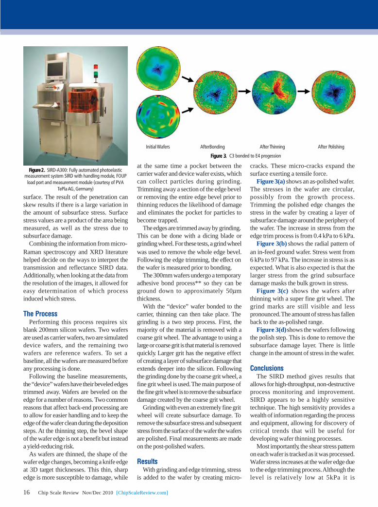
Because of the short measurement time(about 10 min.) and the noncontact andnondestructive method, the system is capableof in-line control and measurements onproduct wafers (Figure 2). Process controlis possible with respect to introduced stressor introduced lattice defects revealed by theirstress fields. Quantification of the stress andclassification of the defects together with theapplicability in all cases where the laser canpenetrate the wafer (transmission limit 10-4) allows a broad field of process controltasks starting from wafer manufacturing upto IC-manufacturing and 3D-integration,especially when abrasive and thermalprocesses are under consideration.
With XRD in the reflective mode, thereis some penetration into the sample’s
FFFFFigure igure igure igure igure 11111..... Optical schema of the scanning infrareddepolarizaiton imager SIRD with the laser unit, the
analyzer unit and the rotation-translation stage wherethe wafer is placed supported by 3 edge pins
Chip Scale Review. Nov/Dec 2010. [ChipScaleReview.com]16
surface. The result of the penetration canskew results if there is a large variation inthe amount of subsurface stress. Surfacestress values are a product of the area beingmeasured, as well as the stress due tosubsurface damage.
Combining the information from micro-Raman spectroscopy and XRD literaturehelped decide on the ways to interpret thetransmission and reflectance SIRD data.Additionally, when looking at the data fromthe resolution of the images, it allowed foreasy determination of which processinduced which stress.
The ProcessPerforming this process requires six
blank 200mm silicon wafers. Two wafersare used as carrier wafers, two are simulateddevice wafers, and the remaining twowafers are reference wafers. To set abaseline, all the wafers are measured beforeany processing is done.
Following the baseline measurements,the “device” wafers have their beveled edgestrimmed away. Wafers are beveled on theedge for a number of reasons. Two commonreasons that affect back-end processing areto allow for easier handling and to keep theedge of the wafer clean during the depositionsteps. At the thinning step, the bevel shapeof the wafer edge is not a benefit but insteada yield-reducing risk.
As wafers are thinned, the shape of thewafer edge changes, becoming a knife edgeat 3D target thicknesses. This thin, sharpedge is more susceptible to damage, while
at the same time a pocket between thecarrier wafer and device wafer exists, whichcan collect particles during grinding.Trimming away a section of the edge bevelor removing the entire edge bevel prior tothinning reduces the likelihood of damageand eliminates the pocket for particles tobecome trapped.
The edges are trimmed away by grinding.This can be done with a dicing blade orgrinding wheel. For these tests, a grind wheelwas used to remove the whole edge bevel.Following the edge trimming, the effect onthe wafer is measured prior to bonding.
The 300mm wafers undergo a temporaryadhesive bond process** so they can beground down to approximately 50μmthickness.
With the “device” wafer bonded to thecarrier, thinning can then take place. Thegrinding is a two step process. First, themajority of the material is removed with acoarse grit wheel. The advantage to using alarge or coarse grit is that material is removedquickly. Larger grit has the negative effectof creating a layer of subsurface damage thatextends deeper into the silicon. Followingthe grinding done by the coarse grit wheel, afine grit wheel is used. The main purpose ofthe fine grit wheel is to remove the subsurfacedamage created by the coarse grit wheel.
Grinding with even an extremely fine gritwheel will create subsurface damage. Toremove the subsurface stress and subsequentstress from the surface of the wafer the wafersare polished. Final measurements are madeon the post-polished wafers.
ResultsWith grinding and edge trimming, stress
is added to the wafer by creating micro-
cracks. These micro-cracks expand thesurface exerting a tensile force.
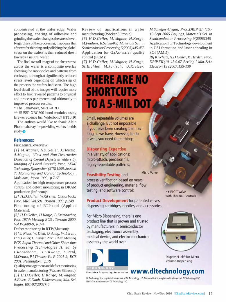
Figure 3(a) shows an as-polished wafer.The stresses in the wafer are circular,possibly from the growth process.Trimming the polished edge changes thestress in the wafer by creating a layer ofsubsurface damage around the periphery ofthe wafer. The increase in stress from theedge trim process is from 0.4 kPa to 6 kPa.
Figure 3(b) shows the radial pattern ofan in-feed ground wafer. Stress went from6 kPa to 97 kPa. The increase in stress is asexpected. What is also expected is that thelarger stress from the grind subsurfacedamage masks the bulk grown in stress.
Figure 3(c) shows the wafers afterthinning with a super fine grit wheel. Thegrind marks are still visible and lesspronounced. The amount of stress has fallenback to the as-polished range.
Figure 3(d) shows the wafers followingthe polish step. This is done to remove thesubsurface damage layer. There is littlechange in the amount of stress in the wafer.
ConclusionsThe SIRD method gives results that
allows for high-throughput, non-destructiveprocess monitoring and improvement.SIRD appears to be a highly sensitivetechnique. The high sensitivity provides awealth of information regarding the processand equipment, allowing for discovery ofcritical trends that will be useful fordeveloping wafer thinning processes.
Most importantly, the shear stress patternon each wafer is tracked as it was processed.Wafer stress increases at the wafer edge dueto the edge trimming process. Although thelevel is relatively low at 5kPa it is
FFFFFigure igure igure igure igure 22222..... SIRD-A300: Fully automated photoelasticmeasurement system SIRD with handling module, FOUP
load port and measurement module (courtesy of PVATePla AG, Germany)
FFFFFigure igure igure igure igure 33333..... C3 bonded to E4 progession
Initial Wafers AfterBonding After Thinning After Polishing
Chip Scale Review. Nov/Dec 2010. [ChipScaleReview.com] 17
concentrated at the wafer edge. Waferprocessing, coating of adhesive andgrinding the wafer changes the stress level.Regardless of the processing, it appears thatafter wafer thinning and polishing the globalstress on the wafers is then reduced downtowards a neutral wafer.
The final overall image of the shear stressacross the wafer is a composite overlayshowing the monopoles and patterns fromeach step, although at significantly reducedstress levels depending on which step ofthe process the wafers had seen. The highlevel detail of the images will require moreeffort to link revealed patterns to physicaland process parameters and ultimately toimproved process results.* The JenaWave, SIRD-ARD** SUSS’ XBC300 bond modules usingBrewer Science Inc. Waferbond? HT10.10
The authors would like to thank AlainPhommahaxay for providing wafers for thisstudy.
References:First general overview:[1] M.Wagner, HD.Geiler, J.Heitzig,A.Mugele; “Fast and Non-DestructiveDetection of Crystal Defects in Wafers byImaging of Local Stress”; Proc. SEMITechnology Symposium (STS) 1999, Session7: Monitoring and Control Technology ,Makuhari, Japan 1999, p.7-65Application for high temperature processcontrol and defect monitoring in DRAMproduction (Infineon):[2] H.D.Geiler, W.Kü rner, O.Storbeck;Proc. MRS Vol.591, Boston 1999, p.249Fine tuning of RTP-tool (AppliedMaterials):[3] H.D.Geiler, H.Karge, B.Krimbacher,Proc 197th Meeting ECS , Toronto 2000,Vol.P-2000-9, p.374Defect monitoring in RTP (Mattson):[4] J. Niess, W. Dietl, O. Altug, W. Lerch ;H.D.Geiler, H.Karge; Proc. 199th MeetingECS, Rapid Thermal and Other Short-timeProcessing Technologies II, ed. byF.Roozeboom, D.L.Kwong, K.Reid,M.Ozturk, P.I.Timans; Vol P-2001-9, ECS2001, Pennington, , p.79Qualitiy management and defect monitoringin wafer manufacturing (Wacker Siltronic):[5] H.D.Geiler, H.Karge, M.Wagner,A.Ehlert, E.Daub, K.Messmann; Mat. Sci.Engin. B91-92(2002)46
Review of applications in wafermanufacturing (Wacker Siltronic):[6] H.D.Geiler, M.Wagner, H.Karge,M.Paulsen, R.Schmolke; Materials Sci. inSemiconductor Processing 5(2003)445-455Application for GaAs-wafer qualitycontrol (FCM):[7] H.D.Geiler, M.Wagner, H.Karge,St.Eichler, M.Jurisch, U.Kretzer,
M.Scheffer-Cygan; Proc.DRIP XI, (15.-19.Sept.2005 Beijing), Materials Sci. inSemiconductor Processing 9(2006)345Application for Technology developmentin USJ formation and laser annealing inSOI (AMD):[8] K.Schulz, H.D.Geiler, M.Herden; Proc.DRIP XII (10.-13.9.07, Berlin), J. Mat. Sci.:Electron 19 (2007)135-139
Chip Scale Review. Nov/Dec 2010. [ChipScaleReview.com]18
3 D glass and silicon interposersface fragmented demand andplenty of competition from other
emerging solutions, but they’re still likelyto be a $950M business by 2015, with avolume of 1.8M 300mm-equivalentwafers. Admittedly, this is a risky forecastfor this emerging market, with its widerange of potential applications anddifferent drivers. But it’s the best estimatebased on close examination of thetechnology’s potential in areas where 3Dinterposers are a clear solution, and of thetrade offs and alternatives in areas whereinterposers are just one of severalpotential competing solutions to thelooming limits of existing technologies.
A 3D interposer can be defined as abridge substrate or carrier that connectsa die to wider-pitched contacts on anotherdie, package, or board, using verticalthrough-via electrical connectionspatterned by photolithography. Currently,3D interposers are already in volumeproduction for products out of the ICmainstream with unique needs, such asMEMS and high brightness LEDs.
Some MEMS manufacturers use a kindof 3D interposer to reduce the cost ofpackaging tiny die. Taking electronicconnections out through vias formed ina wafer-level cap for attachment to theboard allows MEMS chips to be madesignificantly smaller and thus cheaper,bringing down the cost of the packageddevice in spite of the higher cost ofthrough silicon via (TSV) processing.
3D Glass and Silicon Interposers: A $950M Businessby 2015By Jean-Marc Yannou, [Yole Développement]
Jean-Marc Yannou is in charge of advanced packaginganalysis at Yole Développement, including wafer-level pack-aging and 3D system integration. His 15 years of experi-ence in the semiconductor industry include serving as in-novation manager for system-in-package (SiP) technolo-gies at Philips/NXP Semiconductors, and years at TexasInstruments.
High-brightness LED manufacturers arechoosing 3D silicon interposers for betterperformance at lower cost. Historically,they have used flip chip attachment to aceramic sub-mount for heat management,so it’s just a question of replacing ceramicwith silicon. Though ceramic is the betterthermal conductor, silicon can providebetter control of electrostatic discharge andallows smaller devices to reduce cost. Andwith better heat extraction with TSVs,silicon interposers can come close tomatching ceramic for thermalmanagement.
Soon, silicon interposers will bemanufactured in volume production forCMOS image sensors, RF transceivers,and power amplifiers; again driven by thespecific needs of these applications. Thenext generation of image sensorsmarkedly improve sensitivity at lowercost by using backside illumination, aprocess that involves thinning the waferto get the light out the back, andnecessitates the use of interposers withvias to get the electrical contacts out theother side. Some power and RF chips willalso move to using interposers as asolution for improving heat extractionand adding more integrated passives forbetter performance at smaller size.
Near term solution for logic andmemory stacks
In the mainstream logic and memoryIC markets, 3D interposers offer acompelling solution to reduce power
usage in memory stacks and to increaseperformance of the logic-memoryinterface. Memory stacks consume a lotof power in the I/O buffers needed todrive the signals out of the IC. Shorteningthe interconnects by integrating thememory chips with TSVs on interposerscan considerably reduce the number andsize of the required I/O buffers, therebyconsiderably reducing power consumption.
For logic-memory stacks, shorterinterconnects allow for higher frequencyand wider bandwidth for higher speedaccess to memory. Interposers with TSVsbetween the chips currently seems to bethe easiest way to make these stacks,especially as experience using interposersin other niche markets builds processknowhow and potentially reduces costs.
In the long run, standards for padplacement on logic and memory chipscould allow direct chip-to-chipconnections without interposers. JEDECappears to be making a lot of progress onsuch standards that could eventually makeinterposers unnecessary. And designsoftware will likely allow fully integrated3D design, but the tools are far fromready. It is also possible, however, thatinterposers _ like many older ICtechnologies _ will remain a cost-effective solution for some applications.
Finally, interposers are potentially aviable solution to the problem ofconnecting 28nm generation logic _ withits very high I/O density _ to the outsideworld. Chip makers are concerned aboutthe thermal and mechanical mismatchwith current laminates causing reliabilityproblems with ultra low-k dielectrics andcopper pillar flip chip attachment that willbe required at this node. Siliconinterposers that match the thermal andmechanical characteristics of the siliconchip provide a clear solution, though atan added cost. So an R&D push is on tofind new laminate and underfill materialswith lower coefficients of thermalexpansion (CTE) that might potentially
Chip Scale Review. Nov/Dec 2010. [ChipScaleReview.com] 19
solve the mismatch issues at lower cost.But wider experience with 3D siliconinterposers and its alternatives _ likemulticrystalline silicon and volumeproduction on depreciated lines _ are alsolikely to bring down the cost of siliconinterposers.
Wide adoption of these 3D interposerswill also depend on the development of areliable and cost-efficient supply chain.The field is wide open for new playersand business models to capitalize on theopportunity. IDMs, fabless IC suppliers,wafer foundries, packaging houses,MEMS players, substrate makers, andprinted circuit board suppliers are alllooking at taking on this part of the valuechain. While many companies are in theposition to manufacture the interposers,the traditional electronics OEMs aren’tlikely to be able to assemble the more IC-like devices, nor be able to design them.And who will do the testing and takeresponsibility for yield and reliability?Successful suppliers will need to figureout the best ways to organize this new
value chain, whether as system integratorsor partnerships, perhaps involvingspecialty design and test services.
ReferencesThese applications, technologies,
competing solutions, cost issues, likelyplayers and the market size and roadmapare all discussed in detail in YoleDéveloppement’s new report 3D Siliconand Glass Interposers: Technologies,Applications and Markets.
Chip Scale Review. Nov/Dec 2010. [ChipScaleReview.com]20
Copper wire bonding has
become a mainstream packaging
technology for high I/O, fine-
pitch devices. After over a decade of
initially slow-paced R&D, quadrupling of
gold prices over the past five years caused
the electronics packaging industry to
redouble its efforts. This research is now
bearing fruit in fully commercialized, high-
volume production.
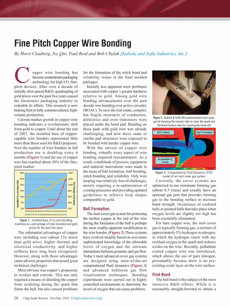
Current market growth in copper wire
bonding indicates a revolutionary shift
from gold to copper. Until about the end
of 2007, the installed base of copper-
capable wire bonders represented little
more than those used for R&D purposes.
Now the number of wire bonders in full
production use is doubling every 6
months (Figure 1) and the use of copper
wire has reached about 20% of the fine-
pitch market.
The substantial advantages of copper
wire including cost (about 15x lower
than gold wire), higher thermal and
electrical conductivity, and higher
stiffness have long been recognized.
However, along with those advantages
came adverse properties that posed great
technical challenges.
Most obvious was copper’s propensity
to oxidize and corrode. This not only
required a means of shielding the copper
from oxidizing during the spark that
forms the ball, but also caused problems
for the formation of the stitch bond and
reliability issues in the final molded
packages.
Initially less apparent were problems
associated with copper’s greater hardness
relative to gold. Among gold wire
bonding advancements over the past
decade was bonding over active circuitry
(BOAC). To save die real estate, complex
but fragile structures of conductors,
dielectrics and even transistors were
placed under the bond pad. Bonding on
these pads with gold wire was already
challenging, and now these same or
similar pad structures were expected to
be bonded with harder copper wire.
With the advent of copper wire
bonding, virtually every aspect of wire
bonding required reexamination. As a
result, a multitude of process, equipment
and material innovations were made in
the areas of ball formation, ball bonding,
stitch bonding and reliability. Only wire
looping was relatively free of challenges,
merely requiring a re-optimization of
existing processes and providing updated
guidelines to achieve loop shapes
comparable to gold.
Ball Formation
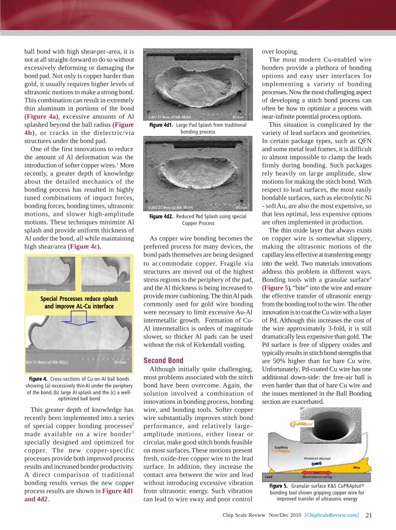
The inert cover-gas system for protecting
the molten copper at the end of the wire
during the formation of the ball is perhaps
the most readily-apparent modification to
the wire bonder. (Figure 2) These systems
have evolved steadily based on ever-more
sophisticated knowledge of the allowable
levels of oxygen and the intricate
interactions between geometry and gas flow.
Today’s most advanced cover gas systems
are designed using state-of-the-art
computational fluid dynamics (Figure 3)
and advanced Schlieren gas flow
visualization techniques. Bonding
experiments were carried out in highly
controlled environments to determine the
levels of oxygen that can cause problems.
Currently, the cover systems are
optimized to use minimum forming gas
(about 0.5 l/min) and usually have an
optional gas port that provides forming
gas to the bonding surface to increase
bond strength. Occurrence of oxidized
balls or pointed balls that take place when
oxygen levels are slightly too high has
been essentially eliminated.
For bare copper wire, the inert cover
gas is typically forming gas; a mixture of
approximately 5% hydrogen in nitrogen,
in which the hydrogen reacts with any
residual oxygen in the spark and reduces
oxides on the wire. Recently, palladium
coated copper wire was introduced,
which allows the use of pure nitrogen,
presumably because there is no pre-
existing oxide layer on the wire surface.
First Bond
The ball bond is the subject of the most
intensive R&D efforts. While it is
reasonably straight-forward to obtain a
Fine Pitch Copper Wire BondingBy Horst Clauberg, Ivy Qin, Paul Reid and Bob Chylak [Kulicke and Soffa Industries, Inc.]
0%
5%
10%
15%
20%
25%
30%
Q4Q4Q1Q2Q3Q4Q1Q2Q3Q4Q1Q2Q3Q4Q1Q2Q3
05 06 07 07 07 07 08 08 08 08 09 09 09 09 10 10 10
Inst
alle
d C
u m
c ba
se (%
)
200
400
600
800
1000
1200
1400
Gol
d pr
ice
($/tr
oy o
z)
Cu mc's
Au price
Figure 1. Installed base of Cu wire bondingmachines as a percentage of total installed and gold
prices for the past five years
Figure 2. Kulicke & Soffa Microenvironment inert cover-gas kit showing the ceramic tube to cover the spark and
the Bond Surface tube for covering the bond site
Figure 3. Computational Fluid Dynamics (CFD)model of an inert cover gas system
Chip Scale Review. Nov/Dec 2010. [ChipScaleReview.com] 21
ball bond with high shear-per-area, it isnot at all straight-forward to do so withoutexcessively deforming or damaging thebond pad. Not only is copper harder thangold, it usually requires higher levels ofultrasonic motions to make a strong bond.This combination can result in extremelythin aluminum in portions of the bond(Figure 4a), excessive amounts of Alsplashed beyond the ball radius (Figure4b) , or cracks in the dielectric/viastructures under the bond pad.
One of the first innovations to reducethe amount of Al deformation was theintroduction of softer copper wires.1 Morerecently, a greater depth of knowledgeabout the detailed mechanics of thebonding process has resulted in highlytuned combinations of impact forces,bonding forces, bonding times, ultrasonicmotions, and slower high-amplitudemotions. These techniques minimize Alsplash and provide uniform thickness ofAl under the bond, all while maintaininghigh shear/area (Figure 4c).
This greater depth of knowledge hasrecently been implemented into a seriesof special copper bonding processes2
made available on a wire bonder3
specially designed and optimized forcopper. The new copper-specificprocesses provide both improved processresults and increased bonder productivity.A direct comparison of traditionalbonding results versus the new copperprocess results are shown in Figure 4d1and 4d2 .
As copper wire bonding becomes thepreferred process for many devices, thebond pads themselves are being designedto accommodate copper. Fragile viastructures are moved out of the higheststress regions to the periphery of the pad,and the Al thickness is being increased toprovide more cushioning. The thin Al padscommonly used for gold wire bondingwere necessary to limit excessive Au-Alintermetallic growth. Formation of Cu-Al intermetallics is orders of magnitudeslower, so thicker Al pads can be usedwithout the risk of Kirkendall voiding.
Second BondAlthough initially quite challenging,
most problems associated with the stitchbond have been overcome. Again, thesolution involved a combination ofinnovations in bonding process, bondingwire, and bonding tools. Softer copperwire substantially improves stitch bondperformance, and relatively large-amplitude motions, either linear orcircular, make good stitch bonds feasibleon most surfaces. These motions presentfresh, oxide-free copper wire to the leadsurface. In addition, they increase thecontact area between the wire and leadwithout introducing excessive vibrationfrom ultrasonic energy. Such vibrationcan lead to wire sway and poor control
over looping.The most modern Cu-enabled wire
bonders provide a plethora of bondingoptions and easy user interfaces forimplementing a variety of bondingprocesses. Now the most challenging aspectof developing a stitch bond process canoften be how to optimize a process withnear-infinite potential process options.
This situation is complicated by thevariety of lead surfaces and geometries.In certain package types, such as QFNand some metal lead frames, it is difficultto almost impossible to clamp the leadsfirmly during bonding. Such packagesrely heavily on large amplitude, slowmotions for making the stitch bond. Withrespect to lead surfaces, the most easilybondable surfaces, such as electrolytic Ni- soft Au, are also the most expensive, sothat less optimal, less expensive optionsare often implemented in production.
The thin oxide layer that always existson copper wire is somewhat slippery,making the ultrasonic motions of thecapillary less effective at transferring energyinto the weld. Two materials innovationsaddress this problem in different ways.Bonding tools with a granular surface4
(Figure 5), “bite” into the wire and ensurethe effective transfer of ultrasonic energyfrom the bonding tool to the wire. The otherinnovation is to coat the Cu wire with a layerof Pd. Although this increases the cost ofthe wire approximately 3-fold, it is stilldramatically less expensive than gold. ThePd surface is free of slippery oxides andtypically results in stitch bond strengths thatare 50% higher than for bare Cu wire.Unfortunately, Pd-coated Cu wire has oneadditional down-side: the free-air ball iseven harder than that of bare Cu wire andthe issues mentioned in the Ball Bondingsection are exacerbated.
FFFFFigure 4.igure 4.igure 4.igure 4.igure 4. Cross-sections of Cu-on-Al ball bondsshowing (a) excessively thin Al under the peripheryof the bond, (b) large Al splash and the (c) a well-
optimized ball bond
Special Processes reduce splashSpecial Processes reduce splashSpecial Processes reduce splashSpecial Processes reduce splashSpecial Processes reduce splashand improve and improve and improve and improve and improve AL-Cu interfaceAL-Cu interfaceAL-Cu interfaceAL-Cu interfaceAL-Cu interface
FFFFFigure 4d1.igure 4d1.igure 4d1.igure 4d1.igure 4d1. Large Pad Splash from traditionalbonding process
FFFFFigure 4d2.igure 4d2.igure 4d2.igure 4d2.igure 4d2. Reduced Pad Splash using specialCopper Process
FFFFFigure 5.igure 5.igure 5.igure 5.igure 5. Granular surface K&S CuPRAplusTM
bonding tool shown gripping copper wire forimproved transfer of ultrasonic energy
Chip Scale Review. Nov/Dec 2010. [ChipScaleReview.com]22
ReliabilityThe use of copper wire bonding in high
volume manufacturing demonstrates thatconfidence in producing reliable packageshas been achieved. When they occur, theroot causes of failures in copper wirebonded packages are radically differentfrom those in gold wire bonding. In Au-to-Al wire bonds, most failures typicallystem from excessive Kirkendall voidingin the rapidly growing intermetalliccompounds. Although these intermetallicsare somewhat sensitive to corrosion, thisaspect of reliability is relatively minor. Asa result, accelerated, unmolded baking ofthe devices provides an accurate predictionof a molded package’s ultimate reliability.Intermetallic coverage is a highly usefulquality measure for Au-Al ball bonds.
In Cu-to-Al bonds, intermetallics growslowly, so that void formation is not aserious problem. Historically, the extremethinness of the intermetallics alsoprevented the process engineer fromperforming an easy check of bond qualityby measuring intermetallic coverage.More recently useful measurements ofintermetallic coverage have emerged.
Further complicating the optimization ofa process for good reliability is the fact thatthe highest shear/area does not correspondto the most reliable Cu bonding process.For Cu ball bonds, shear/area may be wellabove 10g/mil2. In contrast, Au-to-Al bondsusually show a clear maximum near 7g/mil2,and the process with the highest shear/ areawill typically be the most reliable as well.Maximizing shear/area in a copper wirebond only guarantees badly damaged bondpads. Instead, the optimization has to relyon careful and extensive cross-sectioningand etching to verify an even and continuousbond between the Cu and Al.
The next complexity arises from thehigh sensitivity of copper and some of itsaluminum intermetallics to corrosion.Interaction of moisture from highlyaccelerated stress tests (HAST) andpressure cooker tests (PCT) withhalogens and acidic components inmolding compounds are the root-cause ofmany failures. Since the nature of themold compound is one of the key aspectsfor passing reliability tests, the old stand-by of baking unmolded devices as a quickand relatively easy method of screening
Cmpd A Cmpd B Cmpd C
Pd-CuCu
0%
10%
20%
30%
40%
50%
FFFFFigure 6.igure 6.igure 6.igure 6.igure 6. Failure rates after 336 hours biased HAST testfor three experimental mold compound formulations
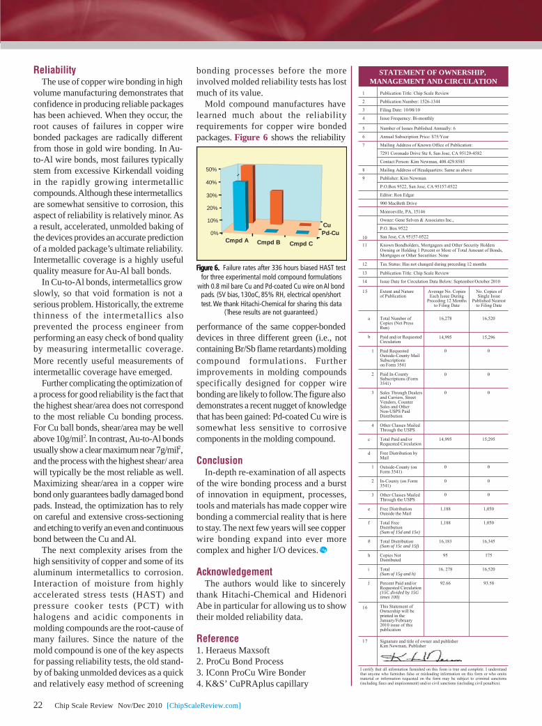
with 0.8 mil bare Cu and Pd-coated Cu wire on Al bondpads. (5V bias, 130oC, 85% RH, electrical open/shorttest. We thank Hitachi-Chemical for sharing this data
(These results are not guaranteed.)
1
2
3
4
5
6
7
Publication Title: Chip Scale Review
Publication Number: 1526-1344
Filing Date: 10/08/10
Issue Frequency: Bi-monthly
Number of Issues Published Annually: 6
Annual Subscription Price: $75/Year
Mailing Address of Known Office of Publication:
8
10
9
900 MacBeth Drive
Monroeville, PA, 15146
Owner: Gene Selven & Associates Inc.,
7291 Coronado Drive Ste 8, San Jose, CA 95129-4582
Contact Person: Kim Newman, 408.429.8585
Mailing Address of Headquarters: Same as above
Publisher: Kim Newman
P.O.Box 9522, San Jose, CA 95157-0522
Editor: Ron Edgar
11
12
13
14
Publication Title: Chip Scale Review
Issue Date for Circulation Data Below: September/October 2010
51
P.O. Box 9522
San Jose, CA 95157-0522
Known Bondholders, Mortgagees and Other Security Holders Owning or Holding 1 Percent or More of Total Amount of Bonds, Mortgages or Other Securities: None
Tax Status: Has not changed during preceding 12 months
a 16,278
b
1
2
3
4
c
d
1
2
3
e
f
g
h
i
j
61
71
STATEMENT OF OWNERSHIP,
MANAGEMENT AND CIRCULATION
Average No. Copies Each Issue During
Preceding 12 Months to Filing Date
No. Copies of Single Issue
Published Nearest to Filing Date
Extent and Nature of Publication
Total Number of Copies (Net Press Run)
Paid and/or Requested Circulation
Paid Requested Outside-County Mail Subscriptionson Form 3541
Paid In-County Subscriptions (Form 3541)
Sales Through Dealers and Carriers, Street Vendors, Counter Sales and Other Non-USPS Paid Distribution
Other Classes Mailed Through the USPS
Total Paid and/or Requested Circulation
Free Distribution by Mail
Outside-County (on Form 3541)
In-County (on Form 3541)
Other Classes Mailed Through the USPS
Free Distribution Outside the Mail
Total Free Distribution(Sum of 15d and 15e)
Total Distribution (Sum of 15c and 15f)
Copies Not Distributed
Total (Sum of 15g and h)
Percent Paid and/or Requested Circulation (15C divided by 15G times 100)
This Statement of Ownership will be printed in the January/February 2010 issue of this publication
16,520
0 0
14,995 15,295
1,188 1,050
1,188 1,050
16,183 16,345
95 175
16 278 16,520
92.66 93.58
14,995 15,296
0 0
0 0
0 0
0 0
0 0
I certify that all information furnished on this form is true and complete. I understand that anyone who furnishes false or misleading information on this form or who omits material or information requested on the form may be subject to criminal sanctions (including fines and imprisonment) and/or civil sanctions (including civil penalties).
Signature and title of owner and publisher Kim Newman, Publisher
bonding processes before the moreinvolved molded reliability tests has lostmuch of its value.
Mold compound manufactures havelearned much about the reliabilityrequirements for copper wire bondedpackages. Figure 6 shows the reliability
performance of the same copper-bondeddevices in three different green (i.e., notcontaining Br/Sb flame retardants) moldingcompound formulations. Furtherimprovements in molding compoundsspecifically designed for copper wirebonding are likely to follow. The figure alsodemonstrates a recent nugget of knowledgethat has been gained: Pd-coated Cu wire issomewhat less sensitive to corrosivecomponents in the molding compound.
ConclusionIn-depth re-examination of all aspects
of the wire bonding process and a burstof innovation in equipment, processes,tools and materials has made copper wirebonding a commercial reality that is hereto stay. The next few years will see copperwire bonding expand into ever morecomplex and higher I/O devices.
AcknowledgementThe authors would like to sincerely
thank Hitachi-Chemical and HidenoriAbe in particular for allowing us to showtheir molded reliability data.
Reference1. Heraeus Maxsoft2. ProCu Bond Process3. IConn ProCu Wire Bonder4. K&S’ CuPRAplus capillary
Chip Scale Review. Nov/Dec 2010. [ChipScaleReview.com]24
Probabilistic Design for Reliability (PDfR)By Ephraim Suhir, [ERS Company, University of California Santa Cruz, University of Maryland College Park]
Reliability Engineering (RE) is part of the AppliedProbabili ty (AP) and Probabilistic Risk
Management (PRM) bodies of knowledge. 1 The termreliability includes dependability, durability, maintainability,repairability, availability, testability, and other properties thatcould or should be viewed and evaluated as probabilities ofthe corresponding reliability characteristics of a device,system, or process. The use of AP and PRM concepts,approaches, and techniques puts the art and practices of REon a solid probabilistic and low-risk foundation.
Accelerated Testing (AT)It is impractical and uneconomical to wait for real-time
failures when the Mean-Time-To-Failure (MTTF) of today’shighly reliable electronic and photonic systems is manythousands of hours. AT is therefore an inevitable and powerfulmeans for understanding, evaluating, and improvingreliability.2,3 This is true for Qualification Testing (QT),testing to pass, or Highly Accelerated Life Testing (HALT),testing to fail. To accelerate a device’s degradation andfailure, one or more conditions that affect functionalperformance, mechanical reliability, or environmentaldurability are deliberately distorted. The major AT categoriesshown in Table 1 differ by their objectives, end points,follow-up activities, and what is viewed as an ideal test.4
QT is the major means through which industry proves thatthe reliability of their products is above a specified level.This level is measured by the percentage of failures per lot,the number of failures per unit time, or both. QT reducesdifferent products, as well as similar products made by
“ You can see a lot by observing.” _ Yogi Berra, American Baseball Player
“It is easy to see, it is hard to foresee.” _ Benjamin Franklin, American Scientist and Statesman
AT Category
Product
Development
Testing (PDT)
Qualification Testing (QT) Highly Accelerated
Life Testing
(HALT)
Objective
Technical feedback toensure that the takendesign approach isviable
Proof of reliability: demonstration that the product is qualified toserve in the given capacity
Understand reliabilityphysics (modes andmechanisms of failure)and assess the likelihoodof failure field
End point
Time, type, level,and/or number of failures
Predetermined time, numberof cycles, and/or the excessive(unexpected) number of failures
Predetermined numberor percentage of failures
Follow-up
Activity
Failure analysis,design decision
Pass/fail decision Failure analysis of thetest data
Ideal Test Specific definitions No failure in a long time Numerous failures ina short time
different manufacturers, to a common denominator. QTreflects the state-of-the-art in a particular field of engineeringand the typical requirements for product performance.Although industry cannot do without QT, today’s QT andspecifications (JEDEC, Telcordia, AEC, or MIL) are onlygood for what they are intended _ to confirm that a givendevice is qualified to become a product. If a device passesexisting QT, it is not always clear why it is good, and if itfails, it is often equally unclear what could be done toimprove its reliability. Since QT, ideally, should not lead toa failure, it is unable to provide the ultimate informationabout reliability _ the probability of the field failure.
HALT, unlike QT, is first of all aimed at understandingthe underlying Physics of Failure (PoF) by detecting possiblefailure modes and mechanisms. Adequately planned,carefully conducted, and properly interpreted, HALTprovides a consistent basis for the prediction of theprobability of failure under given loading (stress) conditionsand after a given time in service. HALT information enableseffective decisions on what could be changed, if necessary,to design and manufacture a reliable product. A functional,structural, material, or technological improvement can betranslated, using HALT data, predictive modeling (PM), andsubsequent sensitivity analyses (SA), into a lower probabilityof field failure. Well-designed and thoroughly implementedHALT can dramatically facilitate the solutions to manyengineering and business-related problems associated withcost effectiveness and time-to-market.
It is highly desirable that HALT is conducted in additionto, and preferably before, QT. There might also be situationswhen HALT can be used as an effective substitution for QT,especially for new products, when suitable QT and standardsdo not yet exist. It is the HALT that reveals the reliabilityphysics behind the product and, ultimately, to create a productwith a low and, if necessary, even specified, predicted, andcontrolled probability of failure. Technical diagnostic,prognostics, and health monitoring and management can playan important role in such an effort. 1,5
Predictive Modeling (PM)HALT, when aimed at the prediction of the likelihood of
the field failure, cannot do without simple and meaningfulTTTTTable 1.able 1.able 1.able 1.able 1. Accelerated Test Categories
Chip Scale Review. Nov/Dec 2010. [ChipScaleReview.com] 25
PM. 6,7 It is on a PM basis that one decides which HALTparameter should be accelerated, how to process theexperimental data, and, most importantly, how to bridge thegap between the HALT data and the likelihood of field failure.By considering the fundamental physics that might constrainthe final design, PM can lead to significant savings of timeand expense. The most widespread HALT models are aimedat predicting the MTTF. Here are some examples and typical use:
Power law (used when PoF is unclear) Boltzmann-Arrhenius equation (used when elevated
temperature is the major cause of failure) Coffin-Manson equation (an inverse power law used to
evaluate low cycle fatigue life-time) Crack growth equations (used to evaluate fracture
toughness of brittle materials) Bueche-Zhurkov and Eyring equations (used to consider
the combined effect of high temperature and mechanicalloading)
Peck equation (to evaluate the combined effect ofelevated temperature and relative humidity)
Black equation (to evaluate the combined effects ofelevated temperature and current density)
Miner-Palmgren rule (to assess fatigue lifetime whenthe yield stress of the material is not exceeded)
Creep rate equations Weakest link model (applicable to extremely brittle
materials with defects) Stress-strength (demand-capacity) interference model,
which is perhaps the most flexible and well substantiatedmodel (Figure 1).
Various predictive models, whether analytical(mathematical) or numerical (simulations), not only thosethat are directly related to HALT, can be extremely helpfulto understand the PoF and to optimize the performance,lifetime, and cost effectiveness of the item of interest.6,7
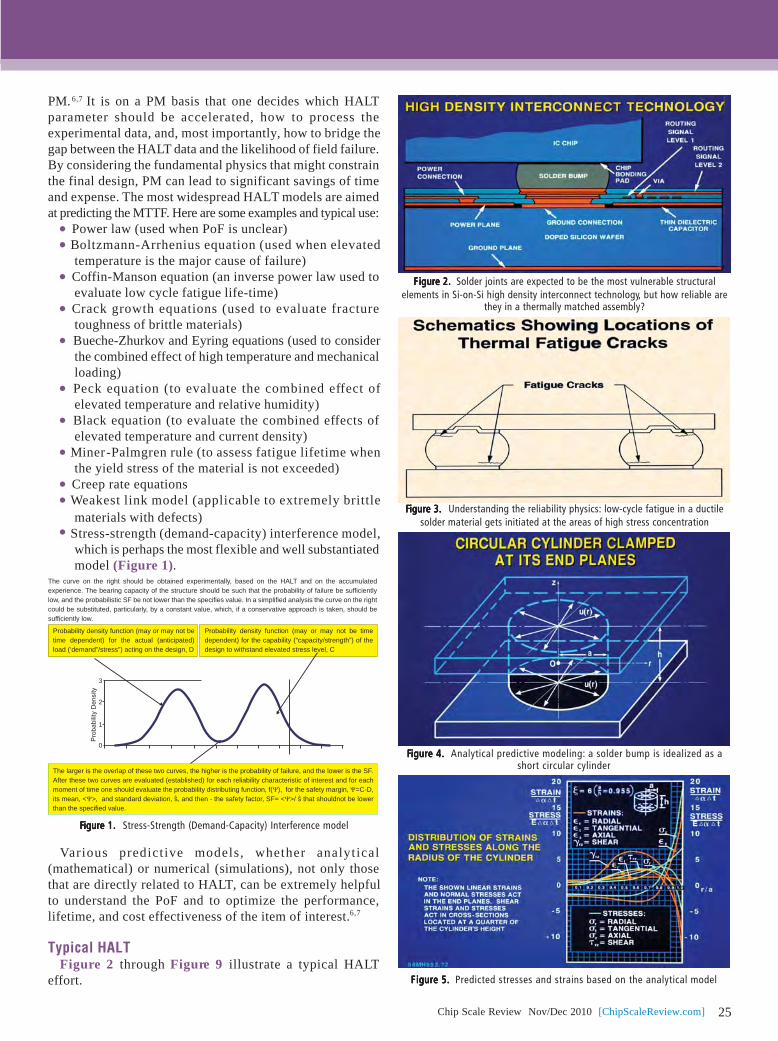
Typical HALTFigure 2 through Figure 9 illustrate a typical HALT
effort.
3
2
1
0
The curve on the right should be obtained experimentally, based on the HALT and on the accumulated experience. The bearing capacity of the structure should be such that the probability of failure be sufficiently low, and the probabilistic SF be not lower than the specifies value. In a simplified analysis the curve on the right could be substituted, particularly, by a constant value, which, if a conservative approach is taken, should be sufficiently low.
Probability density function (may or may not be time dependent) for the actual (anticipated) load (‘demand”/stress”) acting on the design, D
Probability density function (may or may not be time dependent) for the capability (“capacity/strength”) of the design to withstand elevated stress level, C
The larger is the overlap of these two curves, the higher is the probability of failure, and the lower is the SF. After these two curves are evaluated (established) for each reliability characteristic of interest and for each moment of time one should evaluate the probability distributing function, f(Ψ), for the safety margin, Ψ=C-D, its mean, <Ψ>, and standard deviation, s, and then - the safety factor, SF= <Ψ>/ s that shouldnot be lower than the specified value.
FFFFFigure 1.igure 1.igure 1.igure 1.igure 1. Stress-Strength (Demand-Capacity) Interference model
FFFFFigure 2.igure 2.igure 2.igure 2.igure 2. Solder joints are expected to be the most vulnerable structuralelements in Si-on-Si high density interconnect technology, but how reliable are
they in a thermally matched assembly?
FFFFFigure 3.igure 3.igure 3.igure 3.igure 3. Understanding the reliability physics: low-cycle fatigue in a ductilesolder material gets initiated at the areas of high stress concentration
FFFFFigure 4.igure 4.igure 4.igure 4.igure 4. Analytical predictive modeling: a solder bump is idealized as ashort circular cylinder
FFFFFigure 5.igure 5.igure 5.igure 5.igure 5. Predicted stresses and strains based on the analytical model
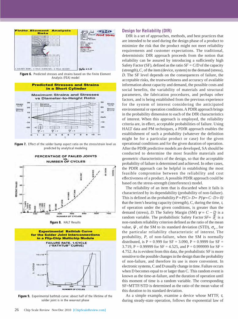
Chip Scale Review. Nov/Dec 2010. [ChipScaleReview.com]26
FFFFFigure 6.igure 6.igure 6.igure 6.igure 6. Predicted stresses and strains based on the Finite ElementAnalysis (FEA) model
FFFFFigure 7.igure 7.igure 7.igure 7.igure 7. Effect of the solder bump aspect ratio on the stress/strain level aspredicted by analytical modeling
FFFFFigure 8.igure 8.igure 8.igure 8.igure 8. HALT Results
FFFFFigure 9.igure 9.igure 9.igure 9.igure 9. Experimental bathtub curve: about half of the lifetime of thesolder joint is in the wear-out phase
Design for Reliability (DfR)DfR is a set of approaches, methods, and best practices that
are intended to be used during the design phase of a product tominimize the risk that the product might not meet reliabilityrequirements and customer expectations. The traditional,deterministic DfR approach proceeds from the notion thatreliability can be assured by introducing a sufficiently highSafety Factor (SF), defined as the ratio SF = C/D of the capacity(strength), C, of the item (device, system) to the demand (stress),D. The SF level depends on the consequences of failure, theacceptable risks, the trustworthiness and accuracy of availableinformation about capacity and demand, the possible costs andsocial benefits, the variability of materials and structuralparameters, the fabrication procedures, and perhaps otherfactors, and is being established from the previous experiencefor the system of interest considering the anticipatedenvironmental or operation conditions. A PDfR approach bringsin the probability dimension to each of the DfR characteristicsof interest. When this approach is employed, the reliabilitycriteria are, in effect, acceptable probabilities of failure. UsingHALT data and PM techniques, a PDfR approach enables theestablishment of such a probability (whatever the definitionmight be for a particular product or case) for the givenoperational conditions and for the given duration of operation.After the PDfR predictive models are developed, SA should beconducted to determine the most feasible materials andgeometric characteristics of the design, so that the acceptableprobability of failure is determined and achieved. In other cases,the PDfR approach can be helpful in establishing the mostfeasible compromise between the reliability and costeffectiveness of a product. A possible PDfR approach could bebased on the stress-strength (interference) model.
The reliability of an item that is discarded when it fails ischaracterized by its dependability (probability of non-failure).This is defined as the probability P = P{C > D = P{ψ = C - D > 0}that the item’s bearing capacity (strength), C, during the time, t,of operation under the given conditions, is greater than thedemand (stress), D. The Safety Margin (SM) ψ = C − D is arandom variable. The probabilistic Safety Factor SF= is anon-random reliability criterion defined as the ratio of the meanvalue, ψ , of the SM to its standard deviation (STD), σψ , forthe particular reliability characteristic of interest. Theprobability, P, of non-failure, when the SM is normallydistributed, is P = 0.999 for SF = 3.090, P = 0.9999 for SF =3.719, P = 0.99999 for SF = 4.525, and P = 0.999999 for SF =4.752. As is evident from this data, the probabilistic SF is moresensitive to the possible changes in the design than the probabilityof non-failure, and therefore its use is more convenient. Inelectronic systems, C and D usually change in time. Failure occurswhen D becomes equal to or larger than C. This random event isknown as the time-at-failure, and the duration of operation untilthis moment of time is a random variable. The correspondingSF=MTTF/STD is determined as the ratio of the mean value ofthis duration to its standard deviation.
As a simple example, examine a device whose MTTF, τ,during steady-state operation, follows the exponential law of
−−
σψ
ψ
−
Chip Scale Review. Nov/Dec 2010. [ChipScaleReview.com]28
reliability and whose PoF can be adequatelycharacterized by the Boltzmann-Arrheniusequation τ = τ0 exp . The failure rateis there fore λ = = exp a n dthe probability of non-failure is P = e-λt=exp exp . Solving this equationfor the absolute temperature, T, we obtainT = . As an example, considera surface charge accumulation failure forwhich = 11600 K, and let the τ0 valuepredicted by HALT be τ0 = 2 x 10 -5hours.Suppose the customer requires that theprobability of failure at the end of thedevice’s service time t = 40,000 hoursdoes not exceed Q = 10-5. Then the aboveformula indicates that the steady-stateoperation temperature should not be higherthan T = 352.3 K = 79.3¡ æand so thethermal management equipment should bedesigned accordingly. This elementaryexample gives a feeling of how the PDfRconcept works and what one could gainby using it. Other examples can be foundin Reference 8 and Reference 9.
As to the reliability of a complexproduct (system), it is characterized, firstof all, by its availability, which is theprobability that the system is available tothe user when needed. High availabilitycan be achieved by employing the mostfeasible combination of dependability onone hand, and repairability, maintainability,and maintenance support on the other.
The most general PDfR approach isbeyond the scope of this article. Thisapproach could be based on the use ofprobability density distribution functionsfor the probabilistic reliabilitycharacteristics of importance (such aselectrical parameters, light output, heattransfer capability, mechanical strength,fracture toughness, maximum/minimumtemperatures, and maximum accelerations/decelerations) and the factors affectingthese characteristics (such as high/lowtemperatures, electrical current/voltage,electrical/optical properties of materials,mechanical and thermal stresses, anddisplacements).
New Qualification Approaches Needed?The short-term, down-to-earth,
practical goal of a device manufactureris to conduct and pass the established QTspecification, without questioningwhether or not it is perfect. The ultimate,
long-term, broad goal of the industry isto make its deliverables reliable in thefield. QT is the major means of makingviable-and-promising devices intoreliable-and-marketable products. It iswell known, however, that devices thatpass existing QT often fail in the field. Isthis indeed a problem? Are the existingQT specifications adequate? Does theindustry need new approaches to qualifyits devices into products? If it does, couldtoday’s QT specifications and proceduresbe improved to an extent that, if thedevice passed these tests, its performancein the field is quantified, predicted, andassured?
We argue that such improvements inQT, as well as in existing best practices,are indeed possible, provided that PDfRmethodologies are widely and consistentlyemployed. One effective way to improvethe existing QT and specifications is todo the following:1. Conduct HALT on a much wider scalethan today, and, if HALT is aimed at theprediction of a field failure, PM must alsobe performed.2. Carry out, whenever and whereverpossible, PM to understand the PoF andto quantify the expected reliability of theproduct3. Revisit, review, and revise the existingQT and specifications based on the HALTdata first considering the most vulnerableelements of the device of interest4. Develop and widely implement thePDfR methodologies keeping in mindthat “nobody and nothing is perfect”, thatthe probability of failure is never zero,but could be specified, predicted,minimized and, if necessary, controlledand maintained at an acceptable low level.
It goes without saying that theseactivities should be conducted on anongoing basis.
If QT has a solid basis in HALT, PM,and PDfR, then there is reason to believethat the product of interest will besufficiently robust in the field. In such asituation, the (still non-destructive) QTcould be viewed as a “quasi-HALT” or an“initial stage of HALT” that more or lessadequately replicates the initial non-destructive stage of HALT. We believe thatsuch an approach to qualify devices intoproducts would enable the industry to
specify, and manufacturers to assure, apredicted and low enough probability offield failure for a device that passed QT.We expect that the suggested approach tothe QT will be accepted by the engineeringand manufacturing communities,implemented into engineering practice andbe adequately reflected in future editions ofthe QT specifications and methodologies.
References1. E. Suhir, “Applied Probability forEngineers and Scientists”, McGraw Hill,New York, 1997.2. E. Suhir, “How to Make a Device into aProduct: Accelerated Life Testing It’sRole, Attributes, Challenges, Pitfalls, andInteraction with Qualification Testing”, inE. Suhir, CP Wong, YC Lee, eds. “Micro-and Opto-Electronic Materials andStructures: Physics, Mechanics, Design,Packaging, Reliability”, Springer, 20073. E.Suhir, “Reliability and Accelerated LifeTesting”, Semiconductor International,February 1, 2005.4. A. Katz, M. Pecht, E. Suhir, “AcceleratedTesting in Microelectronics: Review,Pitfalls and New Developments” Proceedingsof the International Symposium onMicroelectronics and Packaging, IMAPS,Israel, 20005. M.G.Pecht, “Prognostics and HealthManagement in Electronics”, John Wiley,20096. E. Suhir, “Thermo-Mechanical StressModeling in Microelectronics andPhotonics”, Electronic Cooling, vol.7,No.4, 20017. E. Suhir, “Thermal Stress Modeling inMicroelectronics and Photonics Packaging,and the Application of the ProbabilisticApproach: Review and Extension”, IMAPSInternational Journal of Microcircuits andElectronic Packaging, vol.23, No.2, 20008. E. Suhir and B. Poborets, “Solder GlassAttachment in Cerdip/Cerquad Packages:Thermally Induced Stresses andMechanical Reliability”, Proc. of the 40thECTC, Las Vegas, Nevada, May 1990;See also: ASME Journal of ElectronicPackaging, vol. 112, No. 2, 1990.9. E. Suhir, “Probabilistic Approach toEvaluate Improvements in the Reliabilityof Chip-Substrate (Chip-Card) Assembly”,IEEE CPMT Transactions, Part A, vol. 20,No. 1, 1997.
(−UkT )1τ−
1τ0− (−UkT )
([ −UkT )− tτ0− (− ) ]
− −−−U −−k ln [ ( ln P )]τ0
t− −−
Uk−
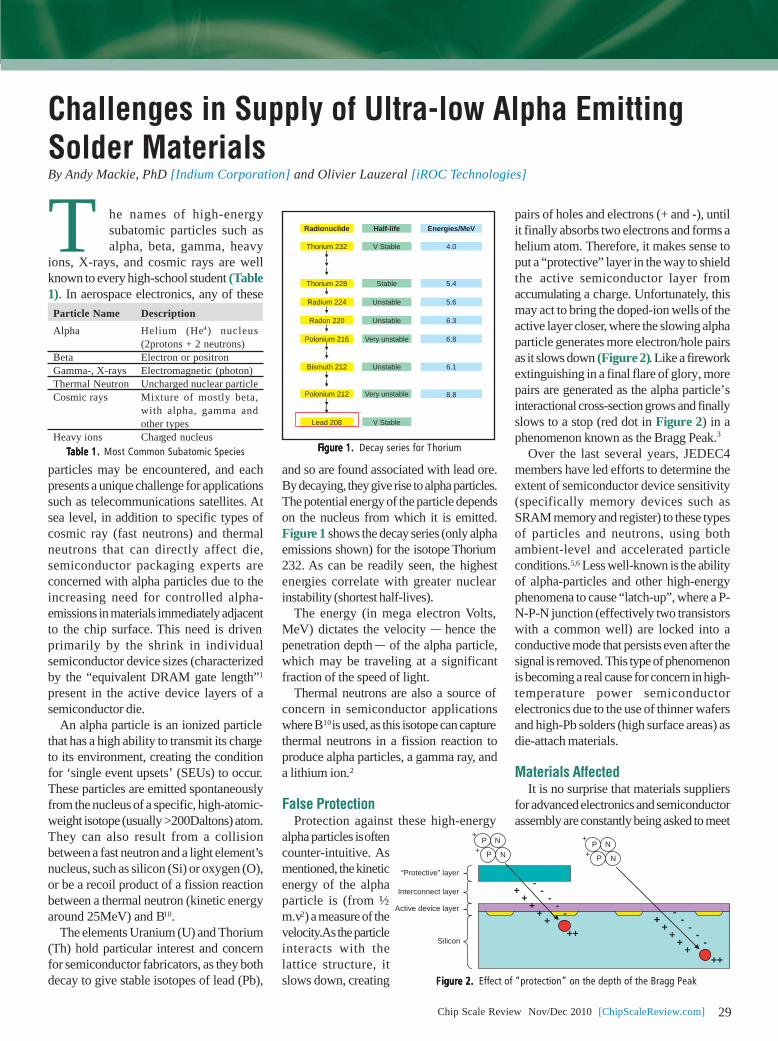
Chip Scale Review. Nov/Dec 2010. [ChipScaleReview.com] 29
T he names of high-energysubatomic particles such asalpha, beta, gamma, heavy
ions, X-rays, and cosmic rays are wellknown to every high-school student (Table1). In aerospace electronics, any of these
particles may be encountered, and eachpresents a unique challenge for applicationssuch as telecommunications satellites. Atsea level, in addition to specific types ofcosmic ray (fast neutrons) and thermalneutrons that can directly affect die,semiconductor packaging experts areconcerned with alpha particles due to theincreasing need for controlled alpha-emissions in materials immediately adjacentto the chip surface. This need is drivenprimarily by the shrink in individualsemiconductor device sizes (characterizedby the “equivalent DRAM gate length”1
present in the active device layers of asemiconductor die.
An alpha particle is an ionized particlethat has a high ability to transmit its chargeto its environment, creating the conditionfor ‘single event upsets’ (SEUs) to occur.These particles are emitted spontaneouslyfrom the nucleus of a specific, high-atomic-weight isotope (usually >200Daltons) atom.They can also result from a collisionbetween a fast neutron and a light element’snucleus, such as silicon (Si) or oxygen (O),or be a recoil product of a fission reactionbetween a thermal neutron (kinetic energyaround 25MeV) and B10.
The elements Uranium (U) and Thorium(Th) hold particular interest and concernfor semiconductor fabricators, as they bothdecay to give stable isotopes of lead (Pb),
Challenges in Supply of Ultra-low Alpha EmittingSolder MaterialsBy Andy Mackie, PhD [Indium Corporation] and Olivier Lauzeral [iROC Technologies]
and so are found associated with lead ore.By decaying, they give rise to alpha particles.The potential energy of the particle dependson the nucleus from which it is emitted.Figure 1 shows the decay series (only alphaemissions shown) for the isotope Thorium232. As can be readily seen, the highestenergies correlate with greater nuclearinstability (shortest half-lives).
The energy (in mega electron Volts,MeV) dictates the velocity _ hence thepenetration depth _ of the alpha particle,which may be traveling at a significantfraction of the speed of light.
Thermal neutrons are also a source ofconcern in semiconductor applicationswhere B10 is used, as this isotope can capturethermal neutrons in a fission reaction toproduce alpha particles, a gamma ray, anda lithium ion.2
False ProtectionProtection against these high-energy
alpha particles is oftencounter-intuitive. Asmentioned, the kineticenergy of the alphaparticle is (from ½m.v2) a measure of thevelocity. As the particleinteracts with thelattice structure, itslows down, creating
pairs of holes and electrons (+ and -), untilit finally absorbs two electrons and forms ahelium atom. Therefore, it makes sense toput a “protective” layer in the way to shieldthe active semiconductor layer fromaccumulating a charge. Unfortunately, thismay act to bring the doped-ion wells of theactive layer closer, where the slowing alphaparticle generates more electron/hole pairsas it slows down (Figure 2). Like a fireworkextinguishing in a final flare of glory, morepairs are generated as the alpha particle’sinteractional cross-section grows and finallyslows to a stop (red dot in Figure 2) in aphenomenon known as the Bragg Peak.3
Over the last several years, JEDEC4members have led efforts to determine theextent of semiconductor device sensitivity(specifically memory devices such asSRAM memory and register) to these typesof particles and neutrons, using bothambient-level and accelerated particleconditions.5,6 Less well-known is the abilityof alpha-particles and other high-energyphenomena to cause “latch-up”, where a P-N-P-N junction (effectively two transistorswith a common well) are locked into aconductive mode that persists even after thesignal is removed. This type of phenomenonis becoming a real cause for concern in high-temperature power semiconductorelectronics due to the use of thinner wafersand high-Pb solders (high surface areas) asdie-attach materials.
Materials AffectedIt is no surprise that materials suppliers
for advanced electronics and semiconductorassembly are constantly being asked to meet
Particle NameAlpha
BetaGamma-, X-raysThermal NeutronCosmic rays
Heavy ions
DescriptionHelium (He4) nucleus(2protons + 2 neutrons)Electron or positronElectromagnetic (photon)Uncharged nuclear particleMixture of mostly beta,with alpha, gamma andother typesCharged nucleus
TTTTTable 1.able 1.able 1.able 1.able 1. Most Common Subatomic Species FFFFFigure 1.igure 1.igure 1.igure 1.igure 1. Decay series for Thorium
FFFFFigure 2.igure 2.igure 2.igure 2.igure 2. Effect of “protection” on the depth of the Bragg Peak
P
P N
N +
+
+ +
+ +
- -
- -
- +
++
P
P N
N +
+
+ +
+ +
- -
- -
- +
++
Silicon
Active device layer
“Protective” layer
Interconnect layer
Radionuclide
Thorium 232
Thorium 228
Radium 224
Radon 220
Polonium 216
Bismuth 212
Polonium 212
Lead 208
Half-life
V Stable
Stable
Unstable
Unstable
Very unstable
Unstable
Very unstable
V Stable
Energies/MeV
4.0
5.4
5.6
6.3
6.8
6.1
8.8
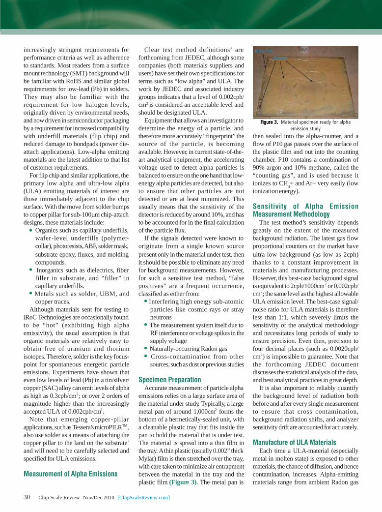
Chip Scale Review. Nov/Dec 2010. [ChipScaleReview.com]30
increasingly stringent requirements forperformance criteria as well as adherenceto standards. Most readers from a surfacemount technology (SMT) background willbe familiar with RoHS and similar globalrequirements for low-lead (Pb) in solders.They may also be familiar with therequirement for low halogen levels,originally driven by environmental needs,and now driven in semiconductor packagingby a requirement for increased compatibilitywith underfill materials (flip chip) andreduced damage to bondpads (power die-attach applications). Low-alpha emittingmaterials are the latest addition to that listof customer requirements.
For flip chip and similar applications, theprimary low alpha and ultra-low alpha(ULA) emitting materials of interest arethose immediately adjacent to the chipsurface. With the move from solder bumpsto copper pillar for sub-100μm chip-attachdesigns, these materials include:
Organics such as capillary underfills,wafer-level underfills (polymer-collar), photoresists, ABF, solder mask,substrate epoxy, fluxes, and moldingcompounds. Inorganics such as dielectrics, fiberfiller in substrate, and “filler” incapillary underfills. Metals such as solder, UBM, andcopper traces.
Although materials sent for testing toiRoC Technologies are occasionally foundto be “hot” (exhibiting high alphaemissivity), the usual assumption is thatorganic materials are relatively easy toobtain free of uranium and thoriumisotopes. Therefore, solder is the key focus-point for spontaneous energetic particleemissions. Experiments have shown thateven low levels of lead (Pb) in a tin/silver/copper (SAC) alloy can emit levels of alphaas high as 0.3cph/cm2; or over 2 orders ofmagnitude higher than the increasinglyaccepted ULA of 0.002cph/cm2.
Note that emerging copper-pillarapplications, such as Tessera’s microPILRTM,also use solder as a means of attaching thecopper pillar to the land on the substrate7
and will need to be carefully selected andspecified for ULA emissions.
Measurement of Alpha Emissions
Clear test method definitions8 areforthcoming from JEDEC, although somecompanies (both materials suppliers andusers) have set their own specifications forterms such as “low alpha” and ULA. Thework by JEDEC and associated industrygroups indicates that a level of 0.002cph/cm2 is considered an acceptable level andshould be designated ULA.
Equipment that allows an investigator todetermine the energy of a particle, andtherefore more accurately “fingerprint” thesource of the particle, is becomingavailable. However, in current state-of-the-art analytical equipment, the acceleratingvoltage used to detect alpha particles isbalanced to ensure on the one hand that low-energy alpha particles are detected, but alsoto ensure that other particles are notdetected or are at least minimized. Thisusually means that the sensitivity of thedetector is reduced by around 10%, and hasto be accounted for in the final calculationof the particle flux.
If the signals detected were known tooriginate from a single known sourcepresent only in the material under test, thenit should be possible to eliminate any needfor background measurements. However,for such a sensitive test method, “falsepositives” are a frequent occurrence,classified as either from:
Interfering high energy sub-atomicparticles like cosmic rays or strayneutrons The measurement system itself due toRF interference or voltage spikes in thesupply voltage Naturally-occurring Radon gas Cross-contamination from othersources, such as dust or previous studies
Specimen PreparationAccurate measurement of particle alpha
emissions relies on a large surface area ofthe material under study. Typically, a largemetal pan of around 1,000cm2 forms thebottom of a hermetically-sealed unit, witha cleanable plastic tray that fits inside thepan to hold the material that is under test.The material is spread into a thin film inthe tray. A thin plastic (usually 0.002” thickMylar) film is then stretched over the tray,with care taken to minimize air entrapmentbetween the material in the tray and theplastic film (Figure 3). The metal pan is
then sealed into the alpha-counter, and aflow of P10 gas passes over the surface ofthe plastic film and out into the countingchamber. P10 contains a combination of90% argon and 10% methane, called the“counting gas”, and is used because itionizes to CH
4+ and Ar+ very easily (low
ionization energy).
Sensitivity of Alpha EmissionMeasurement Methodology
The test method’s sensitivity dependsgreatly on the extent of the measuredbackground radiation. The latest gas flowproportional counters on the market haveultra-low background (as low as 2cph)thanks to a constant improvement inmaterials and manufacturing processes.However, this best-case background signalis equivalent to 2cph/1000cm2 or 0.002cph/cm2; the same level as the highest allowableULA emission level. The best-case signal/noise ratio for ULA materials is thereforeless than 1:1, which severely limits thesensitivity of the analytical methodologyand necessitates long periods of study toensure precision. Even then, precision tofour decimal places (such as 0.0020cph/cm2) is impossible to guarantee. Note thatthe forthcoming JEDEC documentdiscusses the statistical analysis of the data,and best analytical practices in great depth.
It is also important to reliably quantifythe background level of radiation bothbefore and after every single measurementto ensure that cross contamination,background radiation shifts, and analyzersensitivity drift are accounted for accurately.
Manufacture of ULA MaterialsEach time a ULA-material (especially
metal in molten state) is exposed to othermaterials, the chance of diffusion, and hencecontamination, increases. Alpha-emittingmaterials range from ambient Radon gas
FFFFFigure 3.igure 3.igure 3.igure 3.igure 3. Material specimen ready for alphaemission study
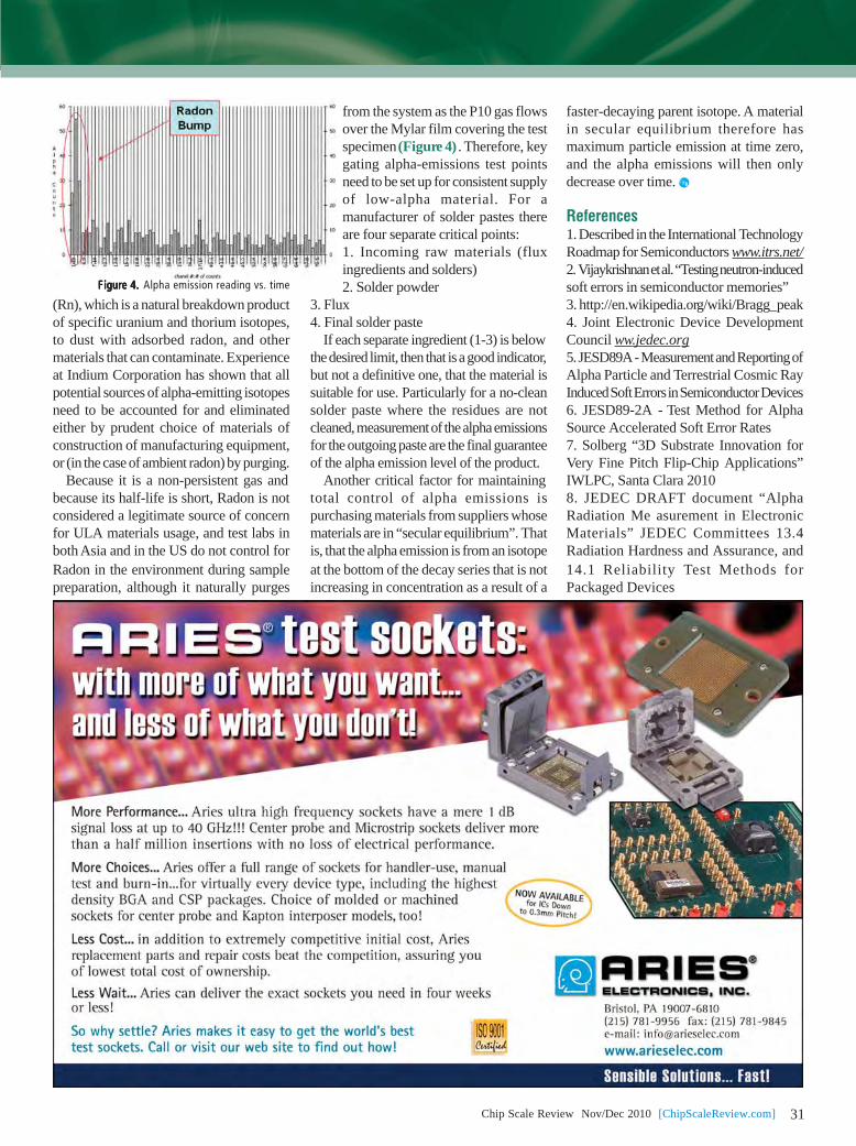
Chip Scale Review. Nov/Dec 2010. [ChipScaleReview.com] 31
FFFFFigure 4.igure 4.igure 4.igure 4.igure 4. Alpha emission reading vs. time
(Rn), which is a natural breakdown productof specific uranium and thorium isotopes,to dust with adsorbed radon, and othermaterials that can contaminate. Experienceat Indium Corporation has shown that allpotential sources of alpha-emitting isotopesneed to be accounted for and eliminatedeither by prudent choice of materials ofconstruction of manufacturing equipment,or (in the case of ambient radon) by purging.
Because it is a non-persistent gas andbecause its half-life is short, Radon is notconsidered a legitimate source of concernfor ULA materials usage, and test labs inboth Asia and in the US do not control forRadon in the environment during samplepreparation, although it naturally purges
from the system as the P10 gas flowsover the Mylar film covering the testspecimen (Figure 4) . Therefore, keygating alpha-emissions test pointsneed to be set up for consistent supplyof low-alpha material. For amanufacturer of solder pastes thereare four separate critical points:1. Incoming raw materials (fluxingredients and solders)2. Solder powder
3. Flux4. Final solder paste
If each separate ingredient (1-3) is belowthe desired limit, then that is a good indicator,but not a definitive one, that the material issuitable for use. Particularly for a no-cleansolder paste where the residues are notcleaned, measurement of the alpha emissionsfor the outgoing paste are the final guaranteeof the alpha emission level of the product.
Another critical factor for maintainingtotal control of alpha emissions ispurchasing materials from suppliers whosematerials are in “secular equilibrium”. Thatis, that the alpha emission is from an isotopeat the bottom of the decay series that is notincreasing in concentration as a result of a
faster-decaying parent isotope. A materialin secular equilibrium therefore hasmaximum particle emission at time zero,and the alpha emissions will then onlydecrease over time.
References1. Described in the International TechnologyRoadmap for Semiconductors www.itrs.net/2. Vijaykrishnan et al. “Testing neutron-inducedsoft errors in semiconductor memories”3. http://en.wikipedia.org/wiki/Bragg_peak4. Joint Electronic Device DevelopmentCouncil ww.jedec.org5. JESD89A - Measurement and Reporting ofAlpha Particle and Terrestrial Cosmic RayInduced Soft Errors in Semiconductor Devices6. JESD89-2A - Test Method for AlphaSource Accelerated Soft Error Rates7. Solberg “3D Substrate Innovation forVery Fine Pitch Flip-Chip Applications”IWLPC, Santa Clara 20108. JEDEC DRAFT document “AlphaRadiation Me asurement in ElectronicMaterials” JEDEC Committees 13.4Radiation Hardness and Assurance, and14.1 Reliability Test Methods forPackaged Devices
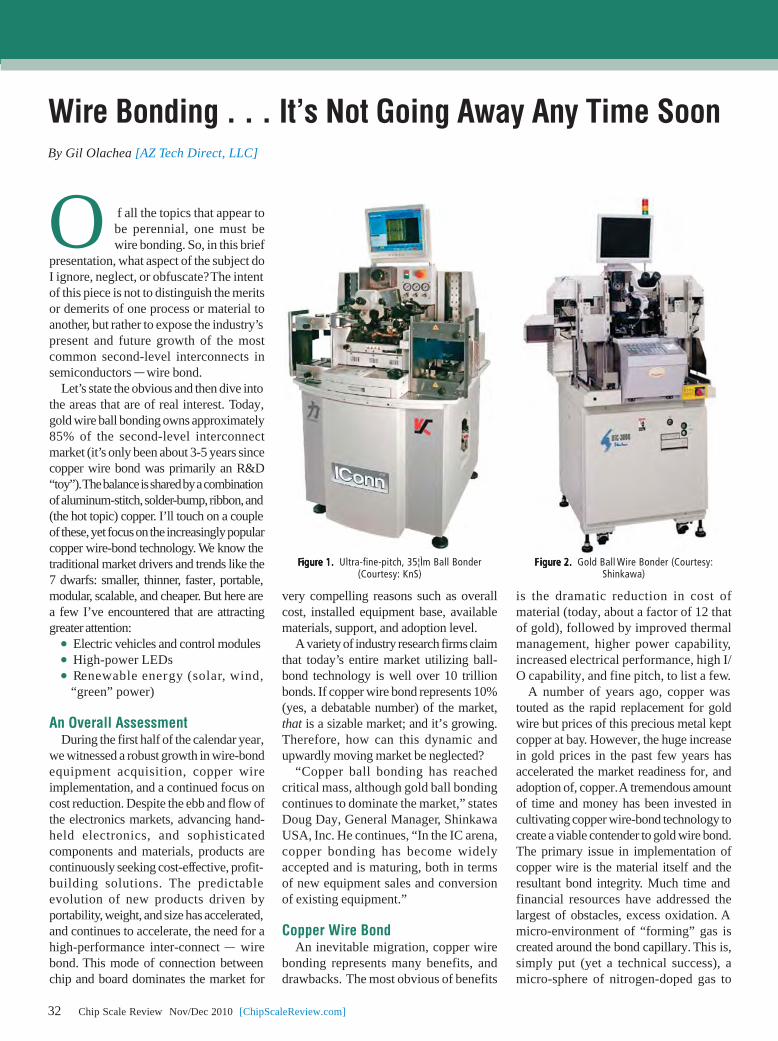
Chip Scale Review. Nov/Dec 2010. [ChipScaleReview.com]32
is the dramatic reduction in cost ofmaterial (today, about a factor of 12 thatof gold), followed by improved thermalmanagement, higher power capability,increased electrical performance, high I/O capability, and fine pitch, to list a few.
A number of years ago, copper wastouted as the rapid replacement for goldwire but prices of this precious metal keptcopper at bay. However, the huge increasein gold prices in the past few years hasaccelerated the market readiness for, andadoption of, copper. A tremendous amountof time and money has been invested incultivating copper wire-bond technology tocreate a viable contender to gold wire bond.The primary issue in implementation ofcopper wire is the material itself and theresultant bond integrity. Much time andfinancial resources have addressed thelargest of obstacles, excess oxidation. Amicro-environment of “forming” gas iscreated around the bond capillary. This is,simply put (yet a technical success), amicro-sphere of nitrogen-doped gas to
Wire Bonding . . . It’s Not Going Away Any Time SoonBy Gil Olachea [AZ Tech Direct, LLC]
f all the topics that appear tobe perennial, one must bewire bonding. So, in this brief
presentation, what aspect of the subject doI ignore, neglect, or obfuscate? The intentof this piece is not to distinguish the meritsor demerits of one process or material toanother, but rather to expose the industry’spresent and future growth of the mostcommon second-level interconnects insemiconductors _ wire bond.
Let’s state the obvious and then dive intothe areas that are of real interest. Today,gold wire ball bonding owns approximately85% of the second-level interconnectmarket (it’s only been about 3-5 years sincecopper wire bond was primarily an R&D“toy”). The balance is shared by a combinationof aluminum-stitch, solder-bump, ribbon, and(the hot topic) copper. I’ll touch on a coupleof these, yet focus on the increasingly popularcopper wire-bond technology. We know thetraditional market drivers and trends like the7 dwarfs: smaller, thinner, faster, portable,modular, scalable, and cheaper. But here area few I’ve encountered that are attractinggreater attention:
Electric vehicles and control modules High-power LEDs Renewable energy (solar, wind,
“green” power)
An Overall AssessmentDuring the first half of the calendar year,
we witnessed a robust growth in wire-bondequipment acquisition, copper wireimplementation, and a continued focus oncost reduction. Despite the ebb and flow ofthe electronics markets, advancing hand-held electronics, and sophisticatedcomponents and materials, products arecontinuously seeking cost-effective, profit-building solutions. The predictableevolution of new products driven byportability, weight, and size has accelerated,and continues to accelerate, the need for ahigh-performance inter-connect _ wirebond. This mode of connection betweenchip and board dominates the market for
O
very compelling reasons such as overallcost, installed equipment base, availablematerials, support, and adoption level.
A variety of industry research firms claimthat today’s entire market utilizing ball-bond technology is well over 10 trillionbonds. If copper wire bond represents 10%(yes, a debatable number) of the market,that is a sizable market; and it’s growing.Therefore, how can this dynamic andupwardly moving market be neglected?
“Copper ball bonding has reachedcritical mass, although gold ball bondingcontinues to dominate the market,” statesDoug Day, General Manager, ShinkawaUSA, Inc. He continues, “In the IC arena,copper bonding has become widelyaccepted and is maturing, both in termsof new equipment sales and conversionof existing equipment.”
Copper Wire BondAn inevitable migration, copper wire
bonding represents many benefits, anddrawbacks. The most obvious of benefits
FFFFFigure 1.igure 1.igure 1.igure 1.igure 1. Ultra-fine-pitch, 35¦Ìm Ball Bonder(Courtesy: KnS)
FFFFFigure 2.igure 2.igure 2.igure 2.igure 2. Gold Ball Wire Bonder (Courtesy:Shinkawa)
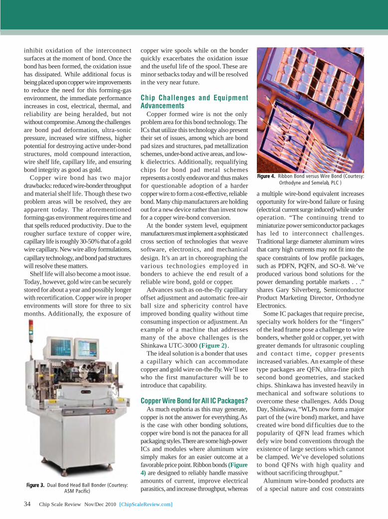
Chip Scale Review. Nov/Dec 2010. [ChipScaleReview.com]34
inhibit oxidation of the interconnectsurfaces at the moment of bond. Once thebond has been formed, the oxidation issuehas dissipated. While additional focus isbeing placed upon copper wire improvementsto reduce the need for this forming-gasenvironment, the immediate performanceincreases in cost, electrical, thermal, andreliability are being heralded, but notwithout compromise. Among the challengesare bond pad deformation, ultra-sonicpressure, increased wire stiffness, higherpotential for destroying active under-bondstructures, mold compound interaction,wire shelf life, capillary life, and ensuringbond integrity as good as gold.
Copper wire bond has two majordrawbacks: reduced wire-bonder throughputand material shelf life. Though these twoproblem areas will be resolved, they areapparent today. The aforementionedforming-gas environment requires time andthat spells reduced productivity. Due to therougher surface texture of copper wire,capillary life is roughly 30-50% that of a goldwire capillary. New wire alloy formulations,capillary technology, and bond pad structureswill resolve these matters.
Shelf life will also become a moot issue.Today, however, gold wire can be securelystored for about a year and possibly longerwith recertification. Copper wire in properenvironments will store for three to sixmonths. Additionally, the exposure of
FFFFFigure 3.igure 3.igure 3.igure 3.igure 3. Dual Bond Head Ball Bonder (Courtesy:ASM Pacific)
copper wire spools while on the bonderquickly exacerbates the oxidation issueand the useful life of the spool. These areminor setbacks today and will be resolvedin the very near future.
Chip Challenges and EquipmentAdvancements
Copper formed wire is not the onlyproblem area for this bond technology. TheICs that utilize this technology also presenttheir set of issues, among which are bondpad sizes and structures, pad metallizationschemes, under-bond active areas, and low-k dielectrics. Additionally, requalifyingchips for bond pad metal schemesrepresents a costly endeavor and thus makesfor questionable adoption of a hardercopper wire to form a cost-effective, reliablebond. Many chip manufacturers are holdingout for a new device rather than invest nowfor a copper wire-bond conversion.
At the bonder system level, equipmentmanufacturers must implement a sophisticatedcross section of technologies that weavesoftware, electronics, and mechanicaldesign. It’s an art in choreographing thevarious technologies employed inbonders to achieve the end result of areliable wire bond, gold or copper.
Advances such as on-the-fly capillaryoffset adjustment and automatic free-airball size and sphericity control haveimproved bonding quality without timeconsuming inspection or adjustment. Anexample of a machine that addressesmany of the above challenges is theShinkawa UTC-3000 (Figure 2) .
The ideal solution is a bonder that usesa capillary which can accommodatecopper and gold wire on-the-fly. We’ll seewho the first manufacturer will be tointroduce that capability.
Copper Wire Bond for All IC Packages?As much euphoria as this may generate,
copper is not the answer for everything. Asis the case with other bonding solutions,copper wire bond is not the panacea for allpackaging styles. There are some high-powerICs and modules where aluminum wiresimply makes for an easier outcome at afavorable price point. Ribbon bonds (Figure4) are designed to reliably handle massiveamounts of current, improve electricalparasitics, and increase throughput, whereas
FFFFFigure 4.igure 4.igure 4.igure 4.igure 4. Ribbon Bond versus Wire Bond (Courtesy:Orthodyne and Semelab, PLC )
a multiple wire-bond equivalent increasesopportunity for wire-bond failure or fusing(electrical current surge induced) while underoperation. “The continuing trend tominiaturize power semiconductor packageshas led to interconnect challenges.Traditional large diameter aluminum wiresthat carry high currents may not fit into thespace constraints of low profile packages,such as PDFN, PQFN, and SO-8. We’veproduced various bond solutions for thepower demanding portable markets . . .”shares Gary Silverberg, SemiconductorProduct Marketing Director, OrthodyneElectronics.
Some IC packages that require precise,specialty work holders for the “fingers”of the lead frame pose a challenge to wirebonders, whether gold or copper, yet withgreater demands for ultrasonic couplingand contact time, copper presentsincreased variables. An example of thesetype packages are QFN, ultra-fine pitchsecond bond geometries, and stackedchips. Shinkawa has invested heavily inmechanical and software solutions toovercome these challenges. Adds DougDay, Shinkawa, “WLPs now form a majorpart of the (wire bond) market, and havecreated wire bond difficulties due to thepopularity of QFN lead frames whichdefy wire bond conventions through theexistence of large sections which cannotbe clamped. We’ve developed solutionsto bond QFNs with high quality andwithout sacrificing throughput.”
Aluminum wire-bonded products areof a special nature and cost constraints
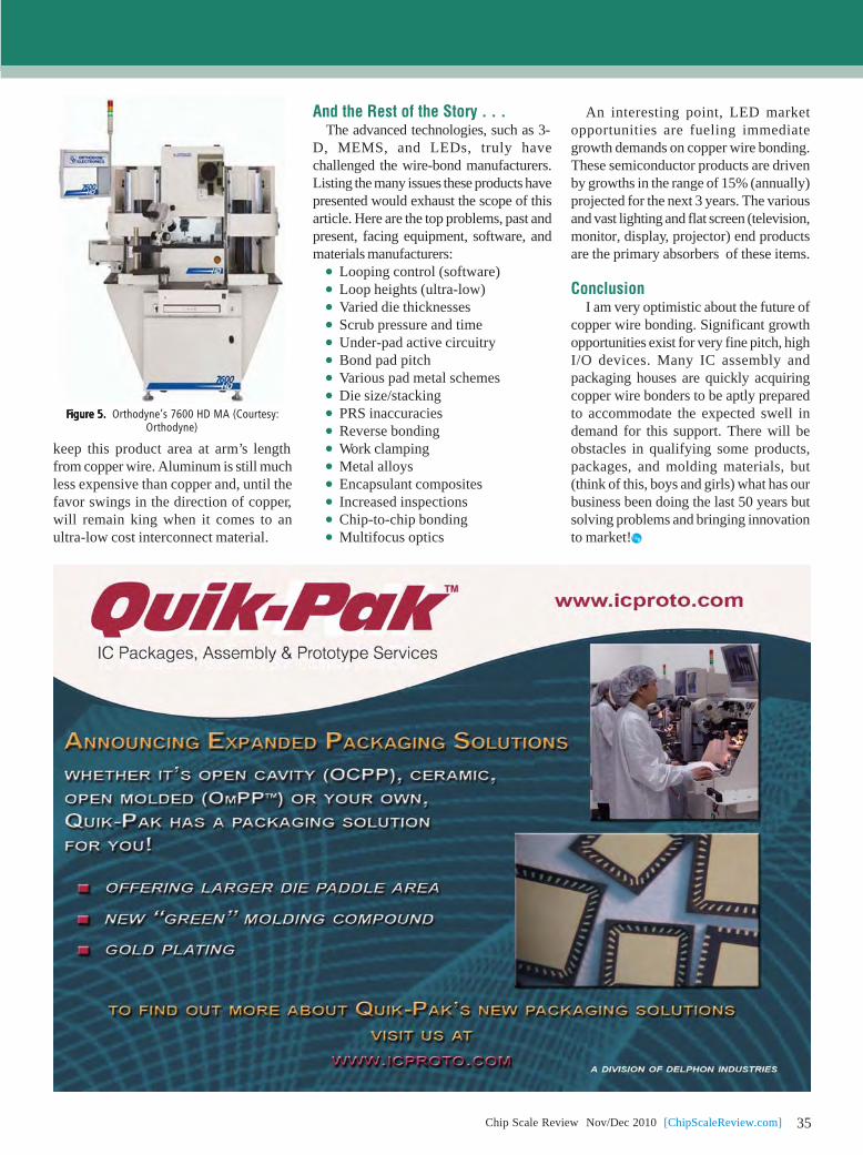
Chip Scale Review. Nov/Dec 2010. [ChipScaleReview.com] 35
keep this product area at arm’s lengthfrom copper wire. Aluminum is still muchless expensive than copper and, until thefavor swings in the direction of copper,will remain king when it comes to anultra-low cost interconnect material.
And the Rest of the Story . . .The advanced technologies, such as 3-
D, MEMS, and LEDs, truly havechallenged the wire-bond manufacturers.Listing the many issues these products havepresented would exhaust the scope of thisarticle. Here are the top problems, past andpresent, facing equipment, software, andmaterials manufacturers:
Looping control (software) Loop heights (ultra-low) Varied die thicknesses Scrub pressure and time Under-pad active circuitry Bond pad pitch Various pad metal schemes Die size/stacking PRS inaccuracies Reverse bonding Work clamping Metal alloys Encapsulant composites Increased inspections Chip-to-chip bonding Multifocus optics
FFFFFigure 5.igure 5.igure 5.igure 5.igure 5. Orthodyne’s 7600 HD MA (Courtesy:Orthodyne)
An interesting point, LED marketopportunities are fueling immediategrowth demands on copper wire bonding.These semiconductor products are drivenby growths in the range of 15% (annually)projected for the next 3 years. The variousand vast lighting and flat screen (television,monitor, display, projector) end productsare the primary absorbers of these items.
ConclusionI am very optimistic about the future of
copper wire bonding. Significant growthopportunities exist for very fine pitch, highI/O devices. Many IC assembly andpackaging houses are quickly acquiringcopper wire bonders to be aptly preparedto accommodate the expected swell indemand for this support. There will beobstacles in qualifying some products,packages, and molding materials, but(think of this, boys and girls) what has ourbusiness been doing the last 50 years butsolving problems and bringing innovationto market!
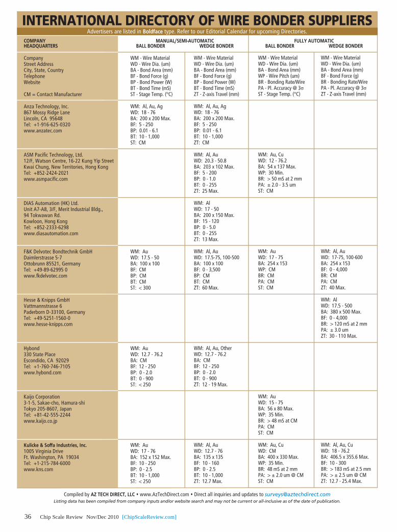
Chip Scale Review. Nov/Dec 2010. [ChipScaleReview.com]36
INTERNATIONAL DIRECTORY OF WIRE BONDER SUPPLIERS
CompanyStreet AddressCity, State, CountryTelephoneWebsite
CM = Contact Manufacturer
Anza Technology, Inc.867 Mossy Ridge LaneLincoln, CA 95648Tel: +1-916-625-0320www.anzatec.com
ASM Pacific Technology, Ltd.12/F, Watson Centre, 16-22 Kung Yip StreetKwai Chung, New Territories, Hong KongTel: +852-2424-2021www.asmpacific.com
DIAS Automation (HK) Ltd.Unit A7-A8, 3/F, Merit Industrial Bldg., 94 Tokwawan Rd.Kowloon, Hong KongTel: +852-2333-6298www.diasautomation.com
F&K Delvotec Bondtechnik GmbHDaimlerstrasse 5-7Ottobrunn 85521, GermanyTel: +49-89-62995 0www.fkdelvotec.com
Hesse & Knipps GmbHVattmannstrasse 6Paderborn D-33100, GermanyTel: +49-5251-1560-0www.hesse-knipps.com
Hybond330 State PlaceEscondido, CA 92029Tel: +1-760-746-7105www.hybond.com
Kaijo Corporation3-1-5, Sakae-cho, Hamura-shiTokyo 205-8607, Japan Tel: +81-42-555-2244www.kaijo.co.jp
Kulicke & Soffa Industries, Inc.1005 Virginia DriveFt. Washington, PA 19034Tel: +1-215-784-6000www.kns.com
WM - Wire MaterialWD - Wire Dia. (um)BA - Bond Area (mm)BF - Bond Force (g)BP - Bond Power (W)BT - Bond Time (mS)ST - Stage Temp. (°C)
WM: Al, Au, AgWD: 18 - 76BA: 200 x 200 Max.BF: 5 - 250BP: 0.01 - 6.1BT: 10 - 1,000ST: CM
WM: AuWD: 17.5 - 50BA: 100 x 100BF: CMBP: CMBT: CMST: < 300
WM: AuWD: 12.7 - 76.2BA: CMBF: 12 - 250BP: 0 - 2.0BT: 0 - 900ST: < 250
WM: AuWD: 17 - 76BA: 152 x 152 Max.BF: 10 - 250BP: 0 - 2.5BT: 10 - 1,000ST: < 250
WM - Wire MaterialWD - Wire Dia. (um)BA - Bond Area (mm)BF - Bond Force (g)BP - Bond Power (W)BT - Bond Time (mS)ZT - Z-axis Travel (mm)
WM: Al, Au, AgWD: 18 - 76BA: 200 x 200 Max.BF: 5 - 250BP: 0.01 - 6.1BT: 10 - 1,000ZT: CM
WM: Al, AuWD: 20.3 - 50.8BA: 203 x 102 Max.BF: 5 - 200BP: 0 - 1.0BT: 0 - 255ZT: 25 Max.
WM: AlWD: 17 - 50BA: 200 x 150 Max.BF: 15 - 120BP: 0 - 5.0BT: 0 - 255ZT: 13 Max.
WM: Al, AuWD: 17.5-75, 100-500BA: 100 x 100BF: 0 - 3,500BP: CMBT: CMZT: 60 Max.
WM: Al, Au, OtherWD: 12.7 - 76.2BA: CMBF: 12 - 250BP: 0 - 2.0BT: 0 - 900ZT: 12 - 19 Max.
WM: Al, AuWD: 12.7 - 76BA: 135 x 135BF: 10 - 160BP: 0 - 2.5BT: 10 - 1,000ZT: 12.7 Max.
WM - Wire MaterialWD - Wire Dia. (um)BA - Bond Area (mm)WP - Wire Pitch (um)BR - Bonding Rate/WirePA - Pl. Accuracy @ 3σST - Stage Temp. (°C)
WM: Au, CuWD: 12 - 76.2BA: 54 x 137 Max.WP: 30 Min.BR: > 50 mS at 2 mmPA: ± 2.0 - 3.5 umST: CM
WM: AuWD: 17 - 75BA: 254 x 153WP: CMBR: CMPA: CMST: CM
WM: AuWD: 15 - 75BA: 56 x 80 Max.WP: 35 Min.BR: > 48 mS at CMPA: CMST: CM
WM: Au, CuWD: CMBA: 400 x 330 Max.WP: 35 Min.BR: 48 mS at 2 mmPA: > ± 2.0 um @ CMST: CM
WM - Wire MaterialWD - Wire Dia. (um)BA - Bond Area (mm)BF - Bond Force (g)BR - Bonding Rate/WirePA - Pl. Accuracy @ 3σZT - Z-axis Travel (mm)
WM: Al, AuWD: 17-75, 100-600BA: 254 x 153BF: 0 - 4,000BR: CMPA: CMZT: 40 Max.
WM: AlWD: 17.5 - 500BA: 380 x 500 Max.BF: 0 - 4,000BR: > 120 mS at 2 mmPA: ± 3.0 umZT: 30 - 110 Max.
WM: Al, Au, CuWD: 18 - 76.2BA: 406.5 x 355.6 Max.BF: 10 - 300BR: > 183 mS at 2.5 mmPA: > ± 2.5 um @ CMZT: 12.7 - 25.4 Max.
COMPANYHEADQUARTERS
MANUAL/SEMI-AUTOMATICBALL BONDER WEDGE BONDER
FULLY AUTOMATICBALL BONDER WEDGE BONDER
Compiled by AZ TECH DIRECT, LLC � www.AzTechDirect.com � Direct all inquiries and updates to [email protected] data has been compiled from company inputs and/or website search and may not be current or all-inclusive as of the date of publication.
Advertisers are listed in Boldface type. Refer to our Editorial Calendar for upcoming Directories.
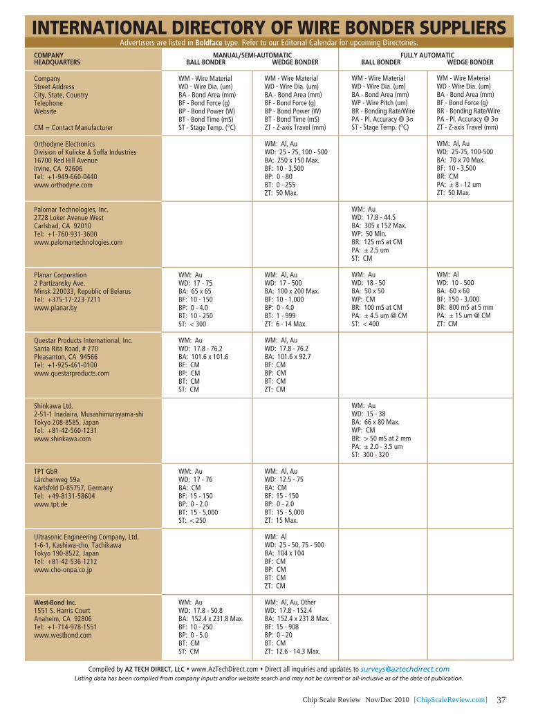
Chip Scale Review. Nov/Dec 2010. [ChipScaleReview.com] 37
INTERNATIONAL DIRECTORY OF WIRE BONDER SUPPLIERS
CompanyStreet AddressCity, State, CountryTelephoneWebsite
CM = Contact Manufacturer
Orthodyne ElectronicsDivision of Kulicke & Soffa Industries16700 Red Hill AvenueIrvine, CA 92606Tel: +1-949-660-0440www.orthodyne.com
Palomar Technologies, Inc.2728 Loker Avenue WestCarlsbad, CA 92010Tel: +1-760-931-3600www.palomartechnologies.com
Planar Corporation2 Partizansky Ave.Minsk 220033, Republic of BelarusTel: +375-17-223-7211www.planar.by
Questar Products International, Inc.Santa Rita Road, # 270Pleasanton, CA 94566Tel: +1-925-461-0100www.questarproducts.com
Shinkawa Ltd.2-51-1 Inadaira, Musashimurayama-shiTokyo 208-8585, JapanTel: +81-42-560-1231www.shinkawa.com
TPT GbRLärchenweg 59aKarlsfeld D-85757, GermanyTel: +49-8131-58604www.tpt.de
Ultrasonic Engineering Company, Ltd.1-6-1, Kashiwa-cho, TachikawaTokyo 190-8522, JapanTel: +81-42-536-1212www.cho-onpa.co.jp
West-Bond Inc.1551 S. Harris CourtAnaheim, CA 92806Tel: +1-714-978-1551www.westbond.com
WM - Wire MaterialWD - Wire Dia. (um)BA - Bond Area (mm)BF - Bond Force (g)BP - Bond Power (W)BT - Bond Time (mS)ST - Stage Temp. (°C)
WM: AuWD: 17 - 75BA: 65 x 65BF: 10 - 150BP: 0 - 4.0BT: 10 - 250ST: < 300
WM: AuWD: 17.8 - 76.2BA: 101.6 x 101.6BF: CMBP: CMBT: CMST: CM
WM: AuWD: 17 - 76BA: CMBF: 15 - 150BP: 0 - 2.0BT: 15 - 5,000ST: < 250
WM: AuWD: 17.8 - 50.8BA: 152.4 x 231.8 Max.BF: 10 - 250BP: 0 - 5.0BT: CMST: CM
WM - Wire MaterialWD - Wire Dia. (um)BA - Bond Area (mm)BF - Bond Force (g)BP - Bond Power (W)BT - Bond Time (mS)ZT - Z-axis Travel (mm)
WM: Al, AuWD: 25 - 75, 100 - 500BA: 250 x 150 Max.BF: 10 - 3,500BP: 0 - 80BT: 0 - 255ZT: 50 Max.
WM: Al, AuWD: 17 - 500BA: 100 x 200 Max.BF: 10 - 1,000BP: 0 - 4.0BT: 1 - 999ZT: 6 - 14 Max.
WM: Al, AuWD: 17.8 - 76.2BA: 101.6 x 92.7BF: CMBP: CMBT: CMZT: CM
WM: Al, AuWD: 12.5 - 75BA: CMBF: 15 - 150BP: 0 - 2.0BT: 15 - 5,000ZT: 15 Max.
WM: AlWD: 25 - 50, 75 - 500BA: 104 x 104BF: CMBP: CMBT: CMZT: CM
WM: Al, Au, OtherWD: 17.8 - 152.4BA: 152.4 x 231.8 Max.BF: 15 - 908BP: 0 - 20BT: CMZT: 12.6 - 14.3 Max.
WM - Wire MaterialWD - Wire Dia. (um)BA - Bond Area (mm)WP - Wire Pitch (um)BR - Bonding Rate/WirePA - Pl. Accuracy @ 3σST - Stage Temp. (°C)
WM: AuWD: 17.8 - 44.5BA: 305 x 152 Max.WP: 50 Min.BR: 125 mS at CMPA: ± 2.5 umST: CM
WM: AuWD: 18 - 50BA: 50 x 50WP: CMBR: 100 mS at CMPA: ± 4.5 um @ CMST: < 400
WM: AuWD: 15 - 38BA: 66 x 80 Max.WP: CMBR: > 50 mS at 2 mmPA: ± 2.0 - 3.5 umST: 300 - 320
WM - Wire MaterialWD - Wire Dia. (um)BA - Bond Area (mm)BF - Bond Force (g)BR - Bonding Rate/WirePA - Pl. Accuracy @ 3σZT - Z-axis Travel (mm)
WM: Al, AuWD: 25-75, 100-500BA: 70 x 70 Max.BF: 10 - 3,500BR: CMPA: ± 8 - 12 umZT: 50 Max.
WM: AlWD: 10 - 500BA: 60 x 60BF: 150 - 3,000BR: 800 mS at 5 mmPA: ± 15 um @ CMZT: CM
COMPANYHEADQUARTERS
MANUAL/SEMI-AUTOMATICBALL BONDER WEDGE BONDER
FULLY AUTOMATICBALL BONDER WEDGE BONDER
Compiled by AZ TECH DIRECT, LLC � www.AzTechDirect.com � Direct all inquiries and updates to [email protected] data has been compiled from company inputs and/or website search and may not be current or all-inclusive as of the date of publication.
Advertisers are listed in Boldface type. Refer to our Editorial Calendar for upcoming Directories.
Chip Scale Review. Nov/Dec 2010. [ChipScaleReview.com]38
afer-level test is a relativelynew paradigm for integratedcircuit (IC) test. Simply put,
it is final test that is performed on a waferprober. Wafer-level test is made possibleby wafer-level packaging (WLP), whichadds a redistribution layer (RDL) to thesurface of each die on the wafer. Theredistribution layer routes signals from thebonding pads to larger pads to which solderballs are added (Figure 1). The redistributionlayer also creates a hermetic seal on the die’sactive surface.
Wafer-level test is mechanically similarto traditional wafer probe. The machineused to manipulate the devices to be tested(the prober) is the same, and the devicesare still attached to one another on the wafer.The addition of the redistribution layer andsolder balls create some mechanicaldifferences (described later).
Electrically, wafer-level test is quitedifferent than traditional wafer probe, whichis typically an abbreviated test performedto confirm that the dice are functional andworth packaging. In recognition thatpackaging affects performance (and also dueto the limitations of most traditional probeinterfaces) a more thorough final test wastraditionally performed after packaging. Sincewafer-level devices are packaged at the waferlevel, the test performed on them is the finaltest, and therefore must be as thorough andcomplete as the traditional package test.
Electrical Challenges of Wafer-levelTest Contacting
When compared to traditional waferprobe, wafer-level contacting presents
Contactors for Wafer-level TestBy Jim Brandes, Multitest
W several electrical challenges for thecontacting hardware. In many cases, thecontacting medium must conduct morecurrent than required for wafer probe. Thisincludes the steady-state current requiredfor the device’s power and ground, as wellas the higher momentary currents thatindividual tests might require. To properlyunderstand the ability of the contacting mediato meet these requirements, they need to bethoroughly characterized by the supplier;tested in the material that is used (not in freeair), at DC and various duty cycles; and witha reasonable temperature rise.
Second, since the wafer-level test mustbe thorough, the contacting medium needs lowinductance to ensure power and ground stabilitywhile the device is switching under load. Forpower delivery, the lower the inductance of thepath, the better it will perform.
There is often a misunderstanding thatlower inductance means better high-frequency performance. This idea resultsfrom the fact that for decades, contact mediahad several nanoHenrys, if not tens of nH,of inductance. At those levels, decreasingthe inductance improved performance.Once inductance is reduced to the point thatit balances capacitance to create a matched-impedance environment, there is no benefit_ but rather a detriment _ to further reduction.
For high-frequency performance,impedance and bandwidth are more importantcharacteristics. Once again it is critical thatthe supplier thoroughly characterize thecontact media for a complete understandingof the high-frequency characteristics, as wellas the parasitic inductance and capacitance.The characterization must also describe thetest conditions, which includes the proximityof signal and return paths, path pitch, anddielectric material at aminimum. It is important toconfirm that the WS testcharacteristics match theconditions under which thecontactor is tested.
And finally, the contactmedium must present a low,consistent resistance to
ensure accurate parametric measurements.In cases of extreme sensitivity to contactresistance (resistance measurements belowan Ohm, critical voltage measurements, orvoltage measurements taken under highcurrent loading) Kelvin contact capability isalso an important consideration.
Mechanical Challenges of Wafer-levelTest Contacting
There are also mechanical challengeswhen comparing wafer-level test totraditional wafer probe.
In traditional wafer probe, contact is madeto relatively clean, extremely coplanar contactpads on each die. Adding the RDL and solderballs greatly increases the coplanaritydeviation of the die. Additionally, the solderballs are not as clean and have a thicker oxidelayer than aluminum or copper bonding pads.
To properly function, the contact mediummust have adequate compliance tocompensate for the coplanarity deviations.(The wafer probe world uses the termoverdrive, which is roughly equivalent tocompliance.) Traditional probe mediamight have tens of microns of overdrive.Wafer-level test requires hundreds ofmicrons of compliance.
The contact medium must also bepresented with sufficient force to penetratethe tin oxide on the typical WLCSP device’ssolder balls. Where 6-10g was sufficientforce for wafer probe, 20-30g is moreappropriate for wafer-level test.
A contact tip geometry that presents asharp profile also aids in the penetration bycreating more pressure per unit of contactforce, and a sharp geometry tends to remainfreer of debris between cleanings. It isimportant to use the proper cleaning
FFFFFigure 1.igure 1.igure 1.igure 1.igure 1. Corner of a WLP, showing bonding pads,redistribution layer, and solder balls
Performance at WS test
Cantilever Probes
Vertical Probes
Membrane Probes
POGO-type Probes
Flat Probes
Inductance 5nH 2 nH 0.2 nH* 1.5 nH 1 nHConductance 0.4 A 0.5 A 0.2 A 1.7 A** 1.8 A**
Bandwidth 2.1 GHz 1.3 GHz 22 GHz 5.5 GHz 18 GHzCompliance 0.05 mm 0.25 mm 0.25 mm 0.5 mm 0.5 mm
Force 6 - 10 g 6 - 25 g 16 g 20 g 25 gInitial Cost $ $$ $$$ $$ $
Field-Servicable Never Sometimes Never Always Always* tip only** Steady-state current. Pulsed current higher.
TTTTTable 1.able 1.able 1.able 1.able 1. Comparison of basic parameters of wafer-level probe technologies
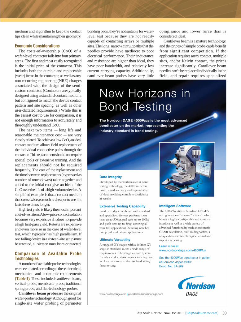
Chip Scale Review. Nov/Dec 2010. [ChipScaleReview.com] 39
medium and algorithm to keep the contacttips clean while maintaining their geometry.
Economic ConsiderationsThe costs-of-ownership (CoO) of a
wafer-level contactor falls into four primaryareas. The first and most easily recognizedis the initial price of the contactor. Thisincludes both the durable and replaceable(wear) items in the contactor, as well as anynon-recurring engineering (NRE) chargesassociated with the design of the semi-custom contactor. (Contactors are typicallydesigned using a standard contact medium,but configured to match the device contactpattern and site spacing, as well as otheruser-dictated requirements.) While this isthe easiest cost to use for comparison, it isnot enough information to accurately andthoroughly understand CoO.
The next two items _ long life andreasonable maintenance cost _ are veryclosely related. To achieve a low CoO, an idealcontact medium allows field replacement ofthe individual conductive paths through thecontactor. This replacement should not requirespecial tools or extensive training. And thereplacements should not be requiredfrequently. The cost of the replacement andthe time between replacements (expressed asnumber of touchdowns) taken together andadded to the initial cost give an idea of theCoO over the life of a high-volume device. Asimplified example is that a contact mediumthat costs twice as much is cheaper to use if itlasts three times longer.
High test yield is likely the most importantcost-of-test item. A low-price contact solutionbecomes very expensive if it does not providea high first-pass yield. Retests are expensiveand even more so in the case of wafer-leveltest, which typically has high parallelism. Ifone failing device in a sixteen-site setup mustbe retested, all sixteen must be re-contacted.
Comparison of Available ProbeTechnologies
A number of available probe technologieswere evaluated according to these electrical,mechanical and economic requirements(Table 1). These included cantilever-beam,vertical-probe, membrane-probe, traditionalspring probe, and flat-technology probes.
Cantilever beam probes are the originalwafer-probe technology. Although good forsingle-site wafer probing of perimeter
bonding pads, they’re not suitable for wafer-level test because they are not readilycapable of contacting arrays or multiplesites. The long, narrow circuit paths that theneedles provide have mediocre to poorelectrical performance. Their inductanceand resistance are higher than ideal, theyhave poor bandwidth, and relatively lowcurrent carrying capacity. Additionally,cantilever beam probes have very little
compliance and lower force than isconsidered ideal.
Cantilever beam is a mature technology,and the prices of simple probe cards benefitfrom significant competition. If theapplication requires array contact, multiplesites, and/or Kelvin contact, the pricesincrease significantly. Cantilever beamneedles can’t be replaced individually in thefield, and repair requires specialized
New Horizons in Bond Testing
Data IntegrityDeveloped by the world leader in bondtesting technology, the 4000Plus offers unsurpassed accuracy and repeatability of data providing complete confidence in results.
Extensive Testing CapabilityLoad cartridges combined with standardand specialized fixtures perform shear tests up to 500kg, pull tests up to 100kgand push tests up to 50kg, covering all your test applications including new hotbump pull and fatigue applications.
Ultimate VersatilityA range of XY stages, with a 160mm XY stage as standard, meets a wide range of requirements. The image capture system for advanced analysis is quick to set-up and in close proximity to the test head aiding faster testing.
www.nordsondage.com | [email protected]
See the 4000Plus bondtester in action at Semicon Japan 2010: Booth No. 8A-209
The Nordson DAGE 4000Plus is the most advanced
bondtester on the market, representing the
industry standard in bond testing.
Intelligent SoftwareThe 4000Plus utilizes Nordson DAGE’s next generation Paragon™ software whichboasts a highly configurable and intuitive interface as well as a wide variety of advanced functionality such as automaticGR&R calculation, built-in diagnostics, aunique database search engine wizard andsuperior reporting.
Learn more at www.nordsondage.com/4000Plus
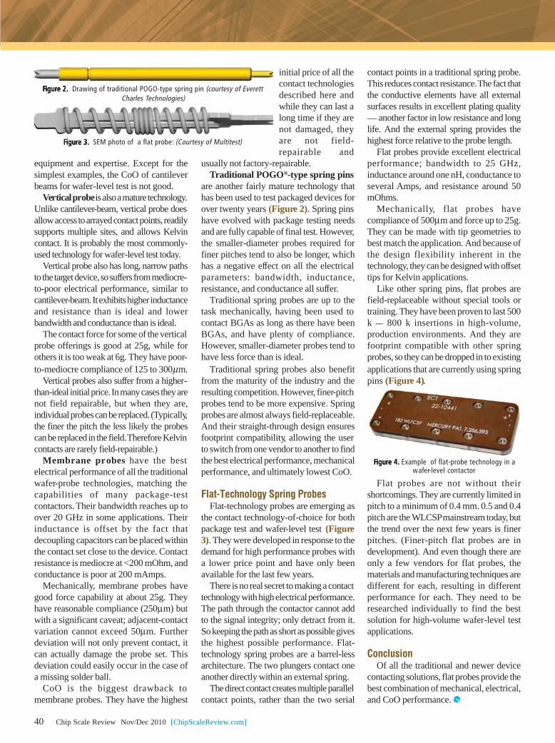
Chip Scale Review. Nov/Dec 2010. [ChipScaleReview.com]40
equipment and expertise. Except for thesimplest examples, the CoO of cantileverbeams for wafer-level test is not good.
Vertical probe is also a mature technology.Unlike cantilever-beam, vertical probe doesallow access to arrayed contact points, readilysupports multiple sites, and allows Kelvincontact. It is probably the most commonly-used technology for wafer-level test today.
Vertical probe also has long, narrow pathsto the target device, so suffers from mediocre-to-poor electrical performance, similar tocantilever-beam. It exhibits higher inductanceand resistance than is ideal and lowerbandwidth and conductance than is ideal.
The contact force for some of the verticalprobe offerings is good at 25g, while forothers it is too weak at 6g. They have poor-to-mediocre compliance of 125 to 300μm.
Vertical probes also suffer from a higher-than-ideal initial price. In many cases they arenot field repairable, but when they are,individual probes can be replaced. (Typically,the finer the pitch the less likely the probescan be replaced in the field. Therefore Kelvincontacts are rarely field-repairable.)
Membrane probes have the bestelectrical performance of all the traditionalwafer-probe technologies, matching thecapabilities of many package-testcontactors. Their bandwidth reaches up toover 20 GHz in some applications. Theirinductance is offset by the fact thatdecoupling capacitors can be placed withinthe contact set close to the device. Contactresistance is mediocre at <200 mOhm, andconductance is poor at 200 mAmps.
Mechanically, membrane probes havegood force capability at about 25g. Theyhave reasonable compliance (250μm) butwith a significant caveat; adjacent-contactvariation cannot exceed 50μm. Furtherdeviation will not only prevent contact, itcan actually damage the probe set. Thisdeviation could easily occur in the case ofa missing solder ball.
CoO is the biggest drawback tomembrane probes. They have the highest
initial price of all thecontact technologiesdescribed here andwhile they can last along time if they arenot damaged, theyare not field-repairable and
usually not factory-repairable.Traditional POGO®-type spring pins
are another fairly mature technology thathas been used to test packaged devices forover twenty years (Figure 2). Spring pinshave evolved with package testing needsand are fully capable of final test. However,the smaller-diameter probes required forfiner pitches tend to also be longer, whichhas a negative effect on all the electricalparameters: bandwidth, inductance,resistance, and conductance all suffer.
Traditional spring probes are up to thetask mechanically, having been used tocontact BGAs as long as there have beenBGAs, and have plenty of compliance.However, smaller-diameter probes tend tohave less force than is ideal.
Traditional spring probes also benefitfrom the maturity of the industry and theresulting competition. However, finer-pitchprobes tend to be more expensive. Springprobes are almost always field-replaceable.And their straight-through design ensuresfootprint compatibility, allowing the userto switch from one vendor to another to findthe best electrical performance, mechanicalperformance, and ultimately lowest CoO.
Flat-Technology Spring ProbesFlat-technology probes are emerging as
the contact technology-of-choice for bothpackage test and wafer-level test (Figure3). They were developed in response to thedemand for high performance probes witha lower price point and have only beenavailable for the last few years.
There is no real secret to making a contacttechnology with high electrical performance.The path through the contactor cannot addto the signal integrity; only detract from it.So keeping the path as short as possible givesthe highest possible performance. Flat-technology spring probes are a barrel-lessarchitecture. The two plungers contact oneanother directly within an external spring.
The direct contact creates multiple parallelcontact points, rather than the two serial
FFFFFigure 2.igure 2.igure 2.igure 2.igure 2. Drawing of traditional POGO-type spring pin (courtesy of EverettCharles Technologies)
FFFFFigure 3.igure 3.igure 3.igure 3.igure 3. SEM photo of a flat probe: (Courtesy of Multitest)
FFFFFigure 4.igure 4.igure 4.igure 4.igure 4. Example of flat-probe technology in awafer-level contactor
contact points in a traditional spring probe.This reduces contact resistance. The fact thatthe conductive elements have all externalsurfaces results in excellent plating quality_ another factor in low resistance and longlife. And the external spring provides thehighest force relative to the probe length.
Flat probes provide excellent electricalperformance; bandwidth to 25 GHz,inductance around one nH, conductance toseveral Amps, and resistance around 50mOhms.
Mechanically, flat probes havecompliance of 500μm and force up to 25g.They can be made with tip geometries tobest match the application. And because ofthe design flexibility inherent in thetechnology, they can be designed with offsettips for Kelvin applications.
Like other spring pins, flat probes arefield-replaceable without special tools ortraining. They have been proven to last 500k _ 800 k insertions in high-volume,production environments. And they arefootprint compatible with other springprobes, so they can be dropped in to existingapplications that are currently using springpins (Figure 4).
Flat probes are not without theirshortcomings. They are currently limited inpitch to a minimum of 0.4 mm. 0.5 and 0.4pitch are the WLCSP mainstream today, butthe trend over the next few years is finerpitches. (Finer-pitch flat probes are indevelopment). And even though there areonly a few vendors for flat probes, thematerials and manufacturing techniques aredifferent for each, resulting in differentperformance for each. They need to beresearched individually to find the bestsolution for high-volume wafer-level testapplications.
ConclusionOf all the traditional and newer device
contacting solutions, flat probes provide thebest combination of mechanical, electrical,and CoO performance.
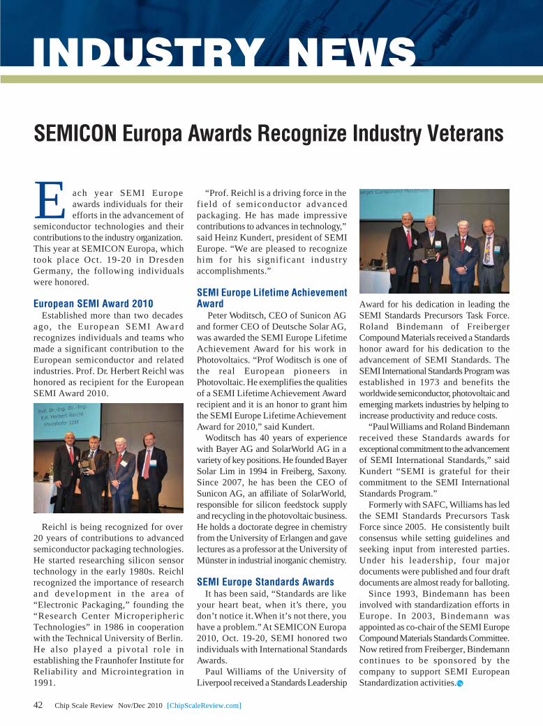
Chip Scale Review. Nov/Dec 2010. [ChipScaleReview.com]42
SEMICON Europa Awards Recognize Industry Veterans
E ach year SEMI Europeawards individuals for theirefforts in the advancement of
semiconductor technologies and theircontributions to the industry organization.This year at SEMICON Europa, whichtook place Oct. 19-20 in DresdenGermany, the following individualswere honored.
European SEMI Award 2010Established more than two decades
ago, the European SEMI Awardrecognizes individuals and teams whomade a significant contribution to theEuropean semiconductor and relatedindustries. Prof. Dr. Herbert Reichl washonored as recipient for the EuropeanSEMI Award 2010.
Reichl is being recognized for over20 years of contributions to advancedsemiconductor packaging technologies.He started researching silicon sensortechnology in the early 1980s. Reichlrecognized the importance of researchand development in the area of“Electronic Packaging,” founding the“Research Center MicroperiphericTechnologies” in 1986 in cooperationwith the Technical University of Berlin.He also played a pivotal role inestablishing the Fraunhofer Institute forReliability and Microintegration in1991.
“Prof. Reichl is a driving force in thefield of semiconductor advancedpackaging. He has made impressivecontributions to advances in technology,”said Heinz Kundert, president of SEMIEurope. “We are pleased to recognizehim for his significant industryaccomplishments.”
SEMI Europe Lifetime AchievementAward
Peter Woditsch, CEO of Sunicon AGand former CEO of Deutsche Solar AG,was awarded the SEMI Europe LifetimeAchievement Award for his work inPhotovoltaics. “Prof Woditsch is one ofthe real European pioneers inPhotovoltaic. He exemplifies the qualitiesof a SEMI Lifetime Achievement Awardrecipient and it is an honor to grant himthe SEMI Europe Lifetime AchievementAward for 2010,” said Kundert.
Woditsch has 40 years of experiencewith Bayer AG and SolarWorld AG in avariety of key positions. He founded BayerSolar Lim in 1994 in Freiberg, Saxony.Since 2007, he has been the CEO ofSunicon AG, an affiliate of SolarWorld,responsible for silicon feedstock supplyand recycling in the photovoltaic business.He holds a doctorate degree in chemistryfrom the University of Erlangen and gavelectures as a professor at the University ofMünster in industrial inorganic chemistry.
SEMI Europe Standards AwardsIt has been said, “Standards are like
your heart beat, when it’s there, youdon’t notice it. When it’s not there, youhave a problem.” At SEMICON Europa2010, Oct. 19-20, SEMI honored twoindividuals with International StandardsAwards.
Paul Williams of the University ofLiverpool received a Standards Leadership
Award for his dedication in leading theSEMI Standards Precursors Task Force.Roland Bindemann of FreibergerCompound Materials received a Standardshonor award for his dedication to theadvancement of SEMI Standards. TheSEMI International Standards Program wasestablished in 1973 and benefits theworldwide semiconductor, photovoltaic andemerging markets industries by helping toincrease productivity and reduce costs.
“Paul Williams and Roland Bindemannreceived these Standards awards forexceptional commitment to the advancementof SEMI International Standards,” saidKundert “SEMI is grateful for theircommitment to the SEMI InternationalStandards Program.”
Formerly with SAFC, Williams has ledthe SEMI Standards Precursors TaskForce since 2005. He consistently builtconsensus while setting guidelines andseeking input from interested parties.Under his leadership, four majordocuments were published and four draftdocuments are almost ready for balloting.
Since 1993, Bindemann has beeninvolved with standardization efforts inEurope. In 2003, Bindemann wasappointed as co-chair of the SEMI EuropeCompound Materials Standards Committee.Now retired from Freiberger, Bindemanncontinues to be sponsored by thecompany to support SEMI EuropeanStandardization activities.
INDUSTRY NEWS
Chip Scale Review. Nov/Dec 2010. [ChipScaleReview.com] 43
Georgia Tech’s PRC establishesUnITE PAC Web Portal
UnITE PAC, which stands forUniversi ty-Industry-Technology-Ecosystem PACkaging, is an industry-academia-government electronics packagingtechnology ecosystem established by the 3DSystems Packaging Research Center atGeorgia Tech. UnITE PAC is designedto advance electronic packagingeducation, technologies, infrastructure,and commercialization via informationdissemination and global networking.
Guided by a board of technicalvisionaries, UnITE PAC was founded on2 simple strategies supported by 3 keyelements in providing world-wide accessto packaging information and resources.The first strategy is to use the internet toprovide individuals, companies andorganizations with a simple, individually-
relevant portal tool where participants caneasily view public domain informationspecific to their posture and needs in theElectronics Packaging Ecosytem. Secondis to establish a series of e-Media andtraditional media communicationsmechanisms leveraging the Internet soparticipants can showcase new information,and learn about emerging technologies,global events, announcements, andresources. The key elements to the programinclude a web portal, webinars andconferences. For more information visitunite.globalgtprc.org/about-unite-pac.
Imec sets up R&D activity in TaiwanImec Taiwan has signed a co-funding
contract with the Taiwanese Ministry ofEconomic Affairs (MOEA) for its R&Dactivity, Imec Taiwan Innovation Centre(ITIC). ITIC’s goal is to expedite appliedresearch projects with industry andacademia that will result in electronicdesigns, components and technology
solutions. The new R&D center will focuson a variety of innovative applications inbioelectronics, MEMS and “green”electronics that are enabled through 3Dsystem-package co-design and system-level evaluation.
Due to the worldwide impact of theTaiwanese semiconductor and consumerelectronics industry, it is an importantmarket for a nanoelectronics R&D centersuch as imec. As imec’s local R&D center,ITIC will reportedly facilitate andintensify the collaboration between imecand the Taiwanese industry and academia.“The creation of ITIC, two years afterhaving established a representation officein Hsinchu, Taiwan, is essential in ourcontinued efforts to create value for ourcurrent and future partners in Taiwan, toleverage our global partnerships, and toactively interact with the Taiwaneseecosystem,” said Luc Van den hove, CEOand President of imec and member of theBoard of imec Taiwan. “An R&D
Chip Scale Review. Nov/Dec 2010. [ChipScaleReview.com]44
INTERNATIONAL DIRECTORY OF WAFER SCRIBING & DICING SYSTEMS
CompanyStreet AddressCity, State, CountryTelephoneWebsite
Note: CM = Contact Manufacturer
Veeco Instruments Inc.Terminal DrivePlainview, NY 11803Tel: +1-516-677-0200www.veeco.com
Method L - Laser, M - Mechanical P - Plasma, S - Saw
Automation LU - Loading & Unloading WA - Wafer Alignment CD - Cleaning & Drying
Specifications (Max.) WD - Wafer Diameter FR - Feed Rate / Speed
Models (Qty)
Method: LaserAutomation: LU, WAWD: 200 mmFR: 600 mm/sModels (2)
Method L - Laser, M - Mechanical P - Plasma, S - Saw
Automation LU - Loading & Unloading WA - Wafer Alignment CD - Cleaning & Drying
Specifications (Max.) WD - Wafer Diameter FR - Feed Rate / Speed
Models (Qty)
Method: SawAutomation: LU, WAWD: 200 mmFR: 600 mm/sModels (2)
Method L - Laser, M - Mechanical P - Plasma, S - Saw
Automation LU - Loading & Unloading WA - Wafer Alignment CD - Cleaning & Drying
Specifications (Max.) WD - Wafer Diameter FR - Feed Rate / Speed
Models (Qty)
Method: LaserAutomation: LU, WAWD: 200 mmFR: 600 mm/sModels (1)
COMPANYHEADQUARTERS
WAFER SCRIBINGSYSTEMS
SAW DICINGSYSTEMS
LASER DICINGSYSTEMS
Compiled by Az Tech Direct, LLC � www.AzTechDirect.com � Direct all inquiries and updates to [email protected] data has been compiled from company inputs and/or website search and may not be current or all-inclusive as of the date of publication.
The listing data for Veeco Instruments Inc was inadvertently omitted from the Sept/Oct International Directory of Wafer Scribing & Dicing Systems Directory.
Advertisers are listed in Boldface type. Refer to our Editorial Calendar for upcoming Directories.
initiative such as ITIC will intensifyimec’s interaction with the localsemiconductor and system-level companiesand academia.”
“As a semiconductor innovativeapplications center, ITIC will supportthe upward shift in Taiwan’s technologyvalue chain and contribute to therealization of Taiwan’s strategicInnovation Plan. It will accelerate openinnovation that will result in locallyowned IP in the area of intelligentelectronics,” says Jung-Chiou Hwang,Vice Minister of Economic Affairs.“The presence of ITIC - the localbranch of the world-famous R&Dcenter imec - will improve Taiwan’sposition against its peers in Asia, andresult in attracting more Europeancompanies to invest in Taiwan.”
John Snyder Appointed VP BusinessDevelopment for AMTECH SolderPaste
In a move expected to grow and expandits AMTECH brand, SMT International,
LLC, manufacturerof AMTECH solderpaste and processsupport products,appointed John Snyderas VP, b u s i n e s sdevelopment. LeighGesick, President of
SMT International, says Snyder is a vitaladdition to the organization.
“We are honored to have John Snyderjoin our organization, as he bringsinvaluable experience as a successfulbusiness executive and as a pioneer in thedevelopment of SMT solder pastetechnology,” notes Gesick. “Mr. Snyderwill assist us in the areas of productdevelopment, marketing/branding, technicalsupport, and territory management.”
“The AMTECH line already containssome very high quality products and issupported by strong technical servicecapabilities managed by very capable andexperienced people, says Snyder. “I wantto take it to another level by helping usfocus on the medical and defense
markets, where domestic demand is stillstrong and product quality andperformance are critically important.Specifically, I want to apply my expertisein new product development by utilizingstatistically designed experiments tocreate a more dynamic product line ableto respond quickly to customer needs.”
An industry veteran with over 30 yearsof experience in polymer chemistry,coatings, powder materials and solderingtechnology, Snyder comes to SMTInternational after a nine year tenure atHeraeus, Inc., where he managed Researchand Development then the operating groupfor the Americas, helping the companyexpand its market share, and opened a newworld class production area. Prior to that,he was VP of Global Technology at AlphaMetals, where he had been since 1989.He’s a graduate of The University ofIllinois majoring in Chemistry andMathematics, and has a long history in newproduct development at variousorganizations including De Soto Inc,Glidden Coatings, and SCM Inc.
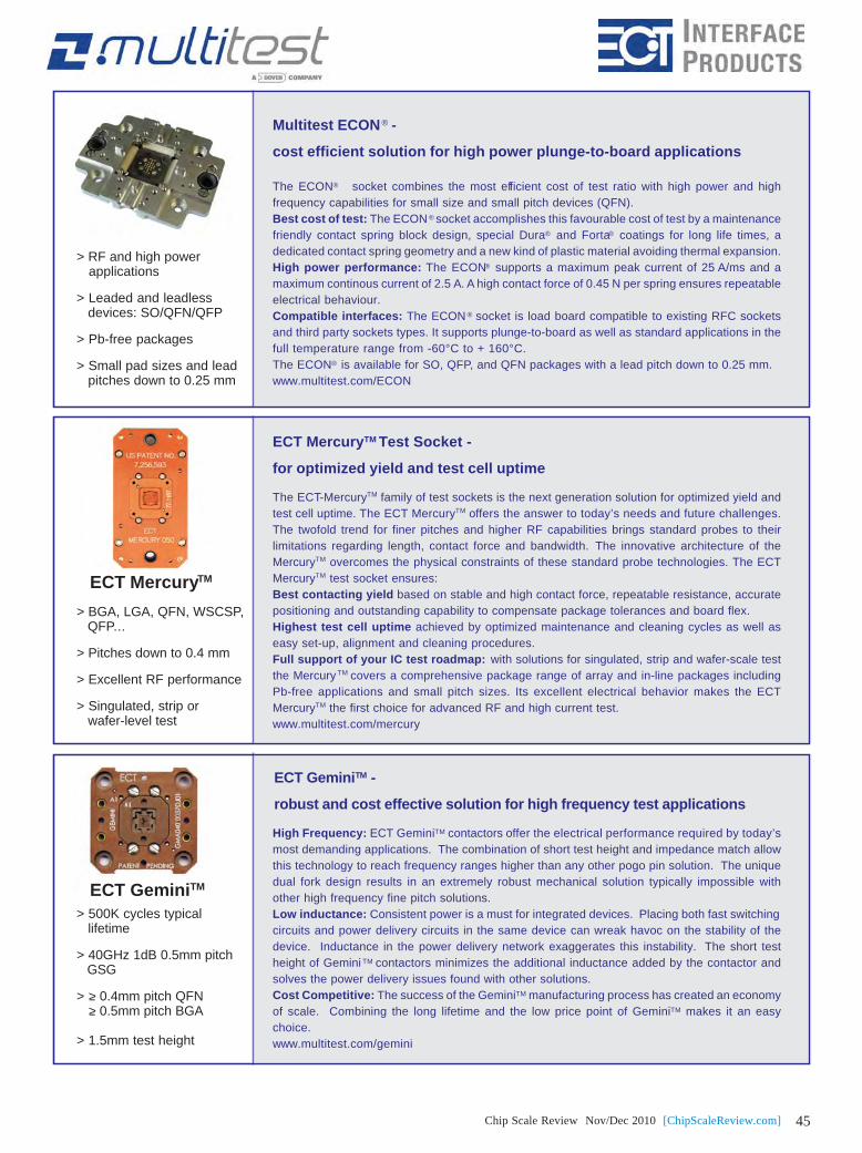
Chip Scale Review. Nov/Dec 2010. [ChipScaleReview.com] 45
ECT MercuryTM
> BGA, LGA, QFN, WSCSP, QFP...
> Pitches down to 0.4 mm
> Excellent RF performance
> Singulated, strip or wafer-level test
The ECT-MercuryTM family of test sockets is the next generation solution for optimized yield andtest cell uptime. The ECT MercuryTM offers the answer to today’s needs and future challenges.The twofold trend for finer pitches and higher RF capabilities brings standard probes to theirlimitations regarding length, contact force and bandwidth. The innovative architecture of theMercuryTM overcomes the physical constraints of these standard probe technologies. The ECTMercuryTM test socket ensures:Best contacting yield based on stable and high contact force, repeatable resistance, accuratepositioning and outstanding capability to compensate package tolerances and board flex.Highest test cell uptime achieved by optimized maintenance and cleaning cycles as well aseasy set-up, alignment and cleaning procedures.Full support of your IC test roadmap: with solutions for singulated, strip and wafer-scale testthe Mercury TM covers a comprehensive package range of array and in-line packages includingPb-free applications and small pitch sizes. Its excellent electrical behavior makes the ECTMercuryTM the first choice for advanced RF and high current test.www.multitest.com/mercury
ECT MercuryTM Test Socket -
for optimized yield and test cell uptime
> RF and high power applications
> Leaded and leadless devices: SO/QFN/QFP
> Pb-free packages
> Small pad sizes and lead pitches down to 0.25 mm
The ECON® socket combines the most efficient cost of test ratio with high power and highfrequency capabilities for small size and small pitch devices (QFN).Best cost of test: The ECON ® socket accomplishes this favourable cost of test by a maintenancefriendly contact spring block design, special Dura® and Forta® coatings for long life times, adedicated contact spring geometry and a new kind of plastic material avoiding thermal expansion.High power performance: The ECON® supports a maximum peak current of 25 A/ms and amaximum continous current of 2.5 A. A high contact force of 0.45 N per spring ensures repeatableelectrical behaviour.Compatible interfaces: The ECON ® socket is load board compatible to existing RFC socketsand third party sockets types. It supports plunge-to-board as well as standard applications in thefull temperature range from -60°C to + 160°C.The ECON® is available for SO, QFP, and QFN packages with a lead pitch down to 0.25 mm.www.multitest.com/ECON
Multitest ECON® -
cost efficient solution for high power plunge-to-board applications
> 500K cycles typical lifetime
> 40GHz 1dB 0.5mm pitch GSG
> >- 0.4mm pitch QFN >- 0.5mm pitch BGA
> 1.5mm test height
High Frequency: ECT GeminiTM contactors offer the electrical performance required by today’smost demanding applications. The combination of short test height and impedance match allowthis technology to reach frequency ranges higher than any other pogo pin solution. The uniquedual fork design results in an extremely robust mechanical solution typically impossible withother high frequency fine pitch solutions.Low inductance: Consistent power is a must for integrated devices. Placing both fast switchingcircuits and power delivery circuits in the same device can wreak havoc on the stability of thedevice. Inductance in the power delivery network exaggerates this instability. The short testheight of Gemini TM contactors minimizes the additional inductance added by the contactor andsolves the power delivery issues found with other solutions.Cost Competitive: The success of the GeminiTM manufacturing process has created an economyof scale. Combining the long lifetime and the low price point of GeminiTM makes it an easychoice.www.multitest.com/gemini
ECT GeminiTM -
robust and cost effective solution for high frequency test applications
ECT GeminiTM
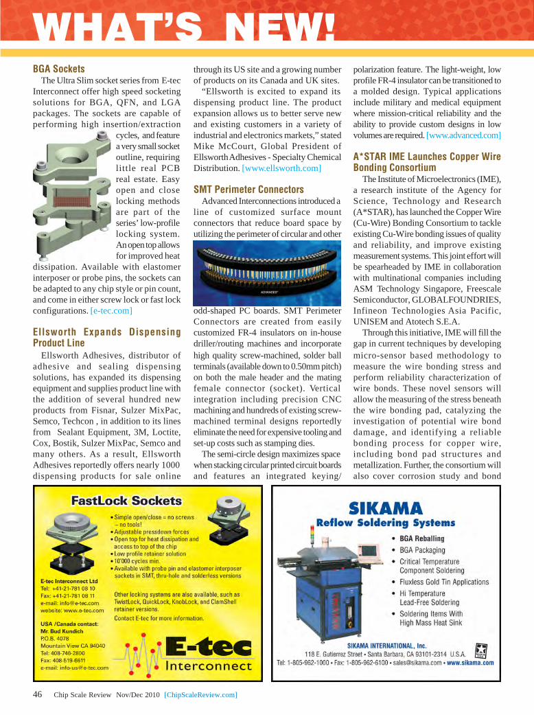
Chip Scale Review. Nov/Dec 2010. [ChipScaleReview.com]46
WHAT'S NEW!BGA Sockets
The Ultra Slim socket series from E-tecInterconnect offer high speed socketingsolutions for BGA, QFN, and LGApackages. The sockets are capable ofperforming high insertion/extraction
cycles, and featurea very small socketoutline, requiringlittle real PCBreal estate. Easyopen and closelocking methodsare part of theseries’ low-profilelocking system.An open top allowsfor improved heat
dissipation. Available with elastomerinterposer or probe pins, the sockets canbe adapted to any chip style or pin count,and come in either screw lock or fast lockconfigurations. [e-tec.com]
Ellsworth Expands DispensingProduct Line
Ellsworth Adhesives, distributor ofadhesive and sealing dispensingsolutions, has expanded its dispensingequipment and supplies product line withthe addition of several hundred newproducts from Fisnar, Sulzer MixPac,Semco, Techcon , in addition to its linesfrom Sealant Equipment, 3M, Loctite,Cox, Bostik, Sulzer MixPac, Semco andmany others. As a result, EllsworthAdhesives reportedly offers nearly 1000dispensing products for sale online
through its US site and a growing numberof products on its Canada and UK sites.
“Ellsworth is excited to expand itsdispensing product line. The productexpansion allows us to better serve newand existing customers in a variety ofindustrial and electronics markets,” statedMike McCourt, Global President ofEllsworth Adhesives - Specialty ChemicalDistribution. [www.ellsworth.com]
SMT Perimeter ConnectorsAdvanced Interconnections introduced a
line of customized surface mountconnectors that reduce board space byutilizing the perimeter of circular and other
odd-shaped PC boards. SMT PerimeterConnectors are created from easilycustomized FR-4 insulators on in-housedriller/routing machines and incorporatehigh quality screw-machined, solder ballterminals (available down to 0.50mm pitch)on both the male header and the matingfemale connector (socket). Verticalintegration including precision CNCmachining and hundreds of existing screw-machined terminal designs reportedlyeliminate the need for expensive tooling andset-up costs such as stamping dies.
The semi-circle design maximizes spacewhen stacking circular printed circuit boardsand features an integrated keying/
polarization feature. The light-weight, lowprofile FR-4 insulator can be transitioned toa molded design. Typical applicationsinclude military and medical equipmentwhere mission-critical reliability and theability to provide custom designs in lowvolumes are required. [www.advanced.com]
A*STAR IME Launches Copper WireBonding Consortium
The Institute of Microelectronics (IME),a research institute of the Agency forScience, Technology and Research(A*STAR), has launched the Copper Wire(Cu-Wire) Bonding Consortium to tackleexisting Cu-Wire bonding issues of qualityand reliability, and improve existingmeasurement systems. This joint effort willbe spearheaded by IME in collaborationwith multinational companies includingASM Technology Singapore, FreescaleSemiconductor, GLOBALFOUNDRIES,Infineon Technologies Asia Pacific,UNISEM and Atotech S.E.A.
Through this initiative, IME will fill thegap in current techniques by developingmicro-sensor based methodology tomeasure the wire bonding stress andperform reliability characterization ofwire bonds. These novel sensors willallow the measuring of the stress beneaththe wire bonding pad, catalyzing theinvestigation of potential wire bonddamage, and identifying a reliablebonding process for copper wire,including bond pad structures andmetallization. Further, the consortium willalso cover corrosion study and bond
Chip Scale Review. Nov/Dec 2010. [ChipScaleReview.com] 47
degradation study related to copper wirebonding in harsh environments.
Electronics Cooler from NextremeThe eTEC TM HV56 module from
Nextreme Thermal Solutions, is the nextproduct in the company’s high-voltage(HV) line of thin-film thermoelectriccoolers (TECs) designed to addresselectronics cooling applications with largerheat pumping requirements. At 0.6mm high,Nextreme claims it to be the thinnest,highest heat pumping TEC on the market.
“Many of our customers have beenasking for a higher wattage device in asingle package,” said Dave Koester, vicepresident of engineering at Nextreme. “TheeTEC HV56 has four times the heatpumping capacity of our HV14 module andoperates at higher voltages, making it easierto drive. The introduction of the HV56 alsodemonstrates our ability to scale up ourtechnology in a variety of configurationsbased on customer requirements.”
At 85oCthe eTEC HV56 can reportedlypump 6 watts or 58 W/cm2 of heat infootprint of only 11 mm2. This creates atemperature differential of up to 60oCbetween its hot and cold sides, and operatesat a maximum voltage of 10.8V, making itcompatible with commonly found board-level currents and voltages. The eTECHV56 is RoHS-compliant and ismanufactured using gold-tin (AuSn) solder,which enables assembly temperatures ashigh as 320oC , making it compatible withindustry standard processes for packagingelectronic devices that require tighttolerances. [www.nextreme.com]
AOI and X-ray InspectionViscom’s X7056 inspection system
combines automatic optical inspection(AOI) with in-line X-ray inspection in onesingle system to detect concealed defectswhile also simultaneously performingselective verification (AXI-onDemand).It’s particularly suited to inspection tasksthat require an AOI with high throughput.Additionally, it is said to reduce false alarmswhile enhancing defect detection capabilities.
Both AOI and X-ray inspectionprocedures can be quickly and easilyperformed using the same user interfacewithout needing to transport assembliesinto a second inspection system. The
system allows for flexibility in meeting inspectionrequirements. The system’s X-ray unit can be used toselectively verify individual defects during inspection tasksthat primarily require an AOI with high throughput,ensuring compliance of tight AOI tolerances.
AXI reportedly provides manufacturers with an effectivequality control because of additional images provided bythe AXI help to reliably assess quality. It can also be usedfor QFN components, where high resolution imagesimprove the user’s ability to reliably evaluate thecomponents. [www.viscom.com]

Chip Scale Review. Nov/Dec 2010. [ChipScaleReview.com]48
West Coast, International Sales & ReprintsKim Newman Chip Scale Review[[email protected]]P.O. Box 9522 San Jose, CA 95157-0522T: 408.429.8585 F: 408.429.8605
Southwest, International & International Directory EntriesRon Molnar AZ Tech Direct[[email protected]]13801 S. 21nd Place Phoenix, AZ 85044T: 480.215.2654 F: 480.496.9451
East CoastRon Friedman [[email protected]]P.O. Box 370183, W. Hartford, CT 06137T: 860.523.1105 F: 860.232.8337
Austria-Germany-SwitzerlandSven Anacker IMP Intermedia Partners GmbH[[email protected]]In der Fleute 46, 42389 Wuppertal, GermanyT: +49.202.27169.17 F: +49.202.27169.20
KoreaKeon Chang Young Media [[email protected]]407 Jinyang Sangga, 120-3 Chungmuro 4 gaChung-ku, Seoul, Korea 100-863T: +82.2.2273.4819 F: +82.2.2273.4866
Advanced Interconnections Corp www.advanced.com ...........................Aries Electronics www.arieselec.com ....................................................AZ Tech Direct www.aztechdirect.com ...................................................BiTS Workship www.bitsworkshop.org ..................................................DL Technology www.dltechnology.com ..................................................Essai www.essai.com .........................................................................E-Tec Interconnect www.e-tec.com .......................................................HCD Corp www.hcdcorp.com ...................................................................Heraeus Materials Technology LLC www.heraeus-contactmaterials.com ......IDI Synergetix www.idinet.com/synergetix ..............................................Kulicke & Soffa Industries Inc www.kns.com .........................................Multitest www.multitest.com ................................................................Newport Corp. www.newport.com/bond1 .............................................Nordson Dage www.nordsondage.com .................................................Powertech Technology Inc www.pti.com.tw ...........................................Protos Electronics www.protoselectronics.com .....................................Pure Technologies www.puretechnologies.com .....................................Quik-Pak www.icproto.com ....................................................................Sensata Technologies www.sensata.com/burninsockets.......................Sikama www.sikama.com ......................................................................SMTA Pan Pac www.smta.org/panpac ...................................................SSEC www.ssecusa.com ......................................................................Transcend Technologies, LLC www.transcendt.com ..............................VI Technology www.vitechnology.com ....................................................Yamaichi Electronics USA (YEU) www.yeu.com .....................................
ADVERTISING SALES
3331474817
OBC465
2797
45IFC3915431935
IBC4641
2-32341
ADVERTISER-INDEX


![The Power of [Taiwan] - SEMI.ORG | Semiconductor Packaging & Testing Service Revenue Taiwan Semiconductor Foundry Service Revenue Semiconductor 4 Semiconductor 5 Taiwan is No. 1 in](https://static.documents.pub/doc/80x56/5ab50d2b7f8b9adc638c9fb0/the-power-of-taiwan-semiorg-semiconductor-packaging-testing-service-revenue.jpg)


