
Rochester Institute of Technology Rochester Institute of Technology
RIT Scholar Works RIT Scholar Works
Theses
5-2020
Theoretical Analysis and Design of Analog Distortion Circuitry Theoretical Analysis and Design of Analog Distortion Circuitry
Daniel Saber [email protected]
Follow this and additional works at: https://scholarworks.rit.edu/theses
Recommended Citation Recommended Citation Saber, Daniel, "Theoretical Analysis and Design of Analog Distortion Circuitry" (2020). Thesis. Rochester Institute of Technology. Accessed from
This Master's Project is brought to you for free and open access by RIT Scholar Works. It has been accepted for inclusion in Theses by an authorized administrator of RIT Scholar Works. For more information, please contact [email protected].
THEORETICAL ANALYSIS AND DESIGN OF ANALOG DISTORTION CIRCUITRY
by
DANIEL SABER
GRADUATE PAPER
Submitted in partial fulfillmentof the requirements for the degree of
MASTER OF SCIENCE
in Electrical Engineering
Approved by:
Mr. Mark A. Indovina, Senior LecturerGraduate Research Advisor, Department of Electrical and Microelectronic Engineering
Dr. Sohail A. Dianat, ProfessorDepartment Head, Department of Electrical and Microelectronic Engineering
DEPARTMENT OF ELECTRICAL AND MICROELECTRONIC ENGINEERING
KATE GLEASON COLLEGE OF ENGINEERING
ROCHESTER INSTITUTE OF TECHNOLOGY
ROCHESTER, NEW YORK
MAY, 2020
I dedicate this work to my father Dr. Eli Saber, my mother Debra Saber, and my brothers Paul
and Joseph Saber.
Declaration
I hereby declare that except where specific reference is made to the work of others, that all
content of this Graduate Paper are original and have not been submitted in whole or in part for
consideration for any other degree or qualification in this, or any other University. This Graduate
Project is the result of my own work and includes nothing which is the outcome of work done in
collaboration, except where specifically indicated in the text.
Daniel Saber
May, 2020

Acknowledgements
I would like to take this opportunity to thank my family. Thank you Paul, Joe, Mom, and Dad
for your continual support throughout my college career. I would also like to thank my friends
for their support as well; the friendships I have made with some of my colleagues have been
invaluable to my success. Lastly, I would like to thank Professor Mark Indovina for offering me
advice, guidance, and setting me up to be successful in my research.
Abstract
The music industry is one that demands the use of modern engineering technologies, such as ef-
fects pedals, in order to achieve a customizable tone for a unique style. Using effects pedals such
as distortion, delay, reverb, and many more, a musician can create a specific tone with distinct
characteristics and adjust certain parameters of the sound to their own preference. This paper
will focus on distortion pedals and the theory revolving around the design of a custom distortion
pedal. Different kinds of distortion require different circuitry and different components. Certain
types of guitar distortion pedals create distortion using simple transistor circuits and/or diode
clipping. Others employ the use of operational amplifiers paired with diodes to create a “dis-
torted” sound. Different musicians may demand various kinds of distortion, and certain types of
distortion are used for different styles. For example, fuzz is a type of distortion which is very
‘messy’ in quality, but widely used for funk, blues, and rock music. There are two main clas-
sifications of distortion: overdrive (soft clipping), and regular distortion (hard clipping). Within
these two categories, many different types of distortion can be produced. Using specific circuitry
is imperative to attaining a specific tonality. By investigating and experimenting with different
designs, this research paper attempts to explain and justify the theory behind the creation of
distortion in a guitar pedal.
Contents
Contents v
List of Figures viii
1 Introduction 1
1.0.1 Research Goals . . . . . . . . . . . . . . . . . . . . . . . . . . . . . . . 2
1.0.2 Contributions . . . . . . . . . . . . . . . . . . . . . . . . . . . . . . . . 3
1.0.3 Organization . . . . . . . . . . . . . . . . . . . . . . . . . . . . . . . . 3
2 Related Work 5
2.1 Introduction . . . . . . . . . . . . . . . . . . . . . . . . . . . . . . . . . . . . . 5
2.2 A Brief History of the Electric Guitar . . . . . . . . . . . . . . . . . . . . . . . 6
2.3 The Electric Guitar: Elementary Concepts . . . . . . . . . . . . . . . . . . . . . 7
2.3.1 Magnetic Guitar Pickups . . . . . . . . . . . . . . . . . . . . . . . . . . 7
2.3.2 Guitar Amplifiers: Valve vs Solid State . . . . . . . . . . . . . . . . . . 10
2.3.3 Guitar Effects Pedals: Analog and Digital Models . . . . . . . . . . . . . 12
2.3.4 Creating Distortion and Overdrive . . . . . . . . . . . . . . . . . . . . . 13
3 Architecture and Implementation of Design 16
3.1 Block Diagram Overview . . . . . . . . . . . . . . . . . . . . . . . . . . . . . . 16
Contents vi
3.1.1 Top Level Block Diagram . . . . . . . . . . . . . . . . . . . . . . . . . 16
3.2 Power Block . . . . . . . . . . . . . . . . . . . . . . . . . . . . . . . . . . . . . 17
3.3 Buffer Stage . . . . . . . . . . . . . . . . . . . . . . . . . . . . . . . . . . . . . 18
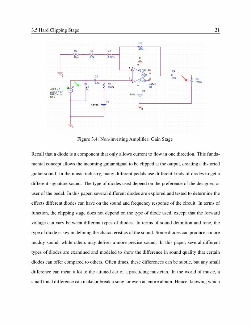
3.4 Gain Stage . . . . . . . . . . . . . . . . . . . . . . . . . . . . . . . . . . . . . . 20
3.5 Hard Clipping Stage . . . . . . . . . . . . . . . . . . . . . . . . . . . . . . . . 20
3.6 Tone Control Stage . . . . . . . . . . . . . . . . . . . . . . . . . . . . . . . . . 23
4 Theoretical Analysis and Design 25
4.1 Fundamental Theoretical Concepts . . . . . . . . . . . . . . . . . . . . . . . . . 25
4.1.1 Operational Amplifiers . . . . . . . . . . . . . . . . . . . . . . . . . . . 25
4.1.2 Diodes and Clipping Circuits . . . . . . . . . . . . . . . . . . . . . . . . 27
4.2 Theoretical Design and Simulation . . . . . . . . . . . . . . . . . . . . . . . . . 31
4.2.1 Buffer Circuit Design . . . . . . . . . . . . . . . . . . . . . . . . . . . . 31
4.2.2 Gain Stage . . . . . . . . . . . . . . . . . . . . . . . . . . . . . . . . . 33
4.2.3 Hard Clipping Stage . . . . . . . . . . . . . . . . . . . . . . . . . . . . 40
4.2.4 Tone Control Stage . . . . . . . . . . . . . . . . . . . . . . . . . . . . . 44
4.3 Complete Analog Circuit: Final Theoretical Simulations . . . . . . . . . . . . . 47
4.3.1 Simulation and Validation . . . . . . . . . . . . . . . . . . . . . . . . . 47
5 Hardware Analysis and Testing 52
5.1 Final Hardware Schematic and PCB Layout . . . . . . . . . . . . . . . . . . . . 52
5.2 Hardware Testing and Validation . . . . . . . . . . . . . . . . . . . . . . . . . . 55
5.2.1 Validation: Buffer Circuit . . . . . . . . . . . . . . . . . . . . . . . . . 55
5.2.2 Validation: Gain Stage with Hard Clipping . . . . . . . . . . . . . . . . 57
5.2.3 Validation: Tone Control Stage . . . . . . . . . . . . . . . . . . . . . . . 61
5.2.4 Validation: Complete Circuit . . . . . . . . . . . . . . . . . . . . . . . . 62
Contents vii
5.3 Modeling of Diodes . . . . . . . . . . . . . . . . . . . . . . . . . . . . . . . . . 62
5.3.1 Diode Hard Clipping Profiles . . . . . . . . . . . . . . . . . . . . . . . 62
5.3.2 Diode Soft Clipping Profiles . . . . . . . . . . . . . . . . . . . . . . . . 71
6 Conclusions 76
6.1 Summary of Results . . . . . . . . . . . . . . . . . . . . . . . . . . . . . . . . . 76
6.2 Outlook and Future Work . . . . . . . . . . . . . . . . . . . . . . . . . . . . . . 77
References 78
I Appendix I-1
I.1 Ibanez Tube Screamer . . . . . . . . . . . . . . . . . . . . . . . . . . . . . . . I-2
I.2 BOSS DS-1 . . . . . . . . . . . . . . . . . . . . . . . . . . . . . . . . . . . . . I-3
I.3 Pedal Enclosure . . . . . . . . . . . . . . . . . . . . . . . . . . . . . . . . . . . I-4
List of Figures
2.1 Single Coil Guitar Pickup [1] . . . . . . . . . . . . . . . . . . . . . . . . . . . . 7
2.2 Magnetic Field as a Function of Vertical Displacement [2] . . . . . . . . . . . . 9
2.3 Changing Magnetic Field Due to Vibrating Wire [2] . . . . . . . . . . . . . . . . 9
2.4 Valve vs Solid State Frequency Response [3] . . . . . . . . . . . . . . . . . . . 11
2.5 Different Types of Clipping by Guitar Amplifiers [4] . . . . . . . . . . . . . . . 12
2.6 Boss DS-1 Block Diagram [5] . . . . . . . . . . . . . . . . . . . . . . . . . . . 15
2.7 General Diode Clipping Circuit [5] . . . . . . . . . . . . . . . . . . . . . . . . . 15
3.1 Top Level Block Diagram . . . . . . . . . . . . . . . . . . . . . . . . . . . . . 17
3.2 Power Block . . . . . . . . . . . . . . . . . . . . . . . . . . . . . . . . . . . . 18
3.3 Buffer Circuit . . . . . . . . . . . . . . . . . . . . . . . . . . . . . . . . . . . . 19
3.4 Non-inverting Amplifier: Gain Stage . . . . . . . . . . . . . . . . . . . . . . . 21
3.5 Hard Clipping Stage . . . . . . . . . . . . . . . . . . . . . . . . . . . . . . . . 22
3.6 Tone Control Stage . . . . . . . . . . . . . . . . . . . . . . . . . . . . . . . . . 24
4.1 Ideal Operational Amplifier [6] . . . . . . . . . . . . . . . . . . . . . . . . . . . 27
4.2 Non-inverting Configuration [6] . . . . . . . . . . . . . . . . . . . . . . . . . . 28
4.3 Diode IV Curve [6] . . . . . . . . . . . . . . . . . . . . . . . . . . . . . . . . . 29
4.4 General Diode Clipping Circuit . . . . . . . . . . . . . . . . . . . . . . . . . . . 31
List of Figures ix
4.5 Buffer Circuit Theoretical Design . . . . . . . . . . . . . . . . . . . . . . . . . 33
4.6 DC Voltages . . . . . . . . . . . . . . . . . . . . . . . . . . . . . . . . . . . . . 34
4.7 Buffer: Theoretical Simulation . . . . . . . . . . . . . . . . . . . . . . . . . . . 34
4.8 Theoretical Schematic: Gain Stage . . . . . . . . . . . . . . . . . . . . . . . . . 35
4.9 Minimum Gain Setting: Potentiometer = 1MΩ . . . . . . . . . . . . . . . . . . . 37
4.10 Potentiometer = 250kΩ . . . . . . . . . . . . . . . . . . . . . . . . . . . . . . . 37
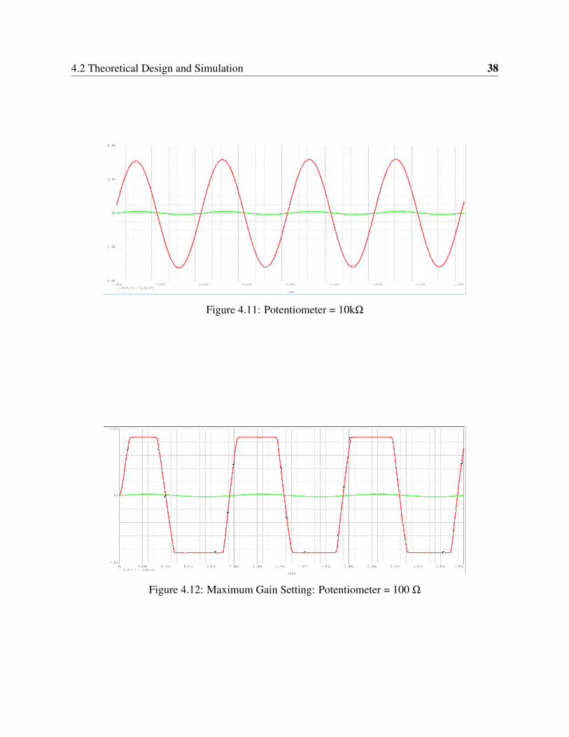
4.11 Potentiometer = 10kΩ . . . . . . . . . . . . . . . . . . . . . . . . . . . . . . . . 38
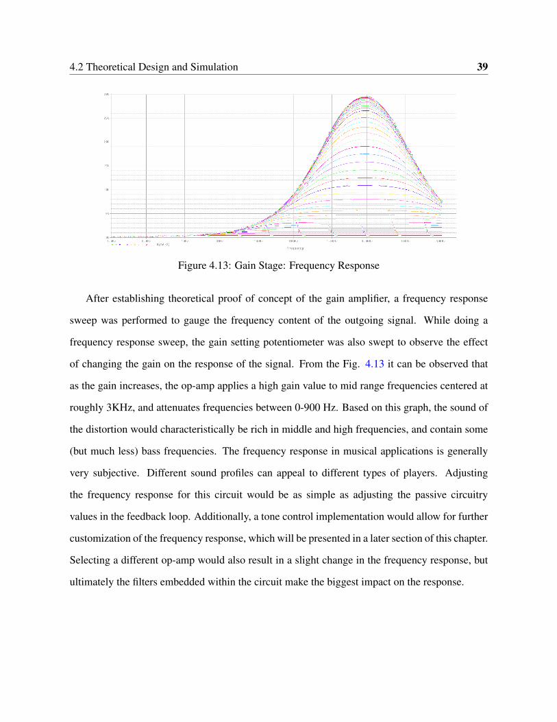
4.12 Maximum Gain Setting: Potentiometer = 100 Ω . . . . . . . . . . . . . . . . . . 38
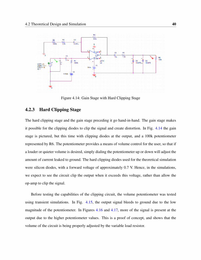
4.13 Gain Stage: Frequency Response . . . . . . . . . . . . . . . . . . . . . . . . . . 39
4.14 Gain Stage with Hard Clipping Stage . . . . . . . . . . . . . . . . . . . . . . . . 40
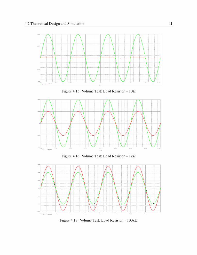
4.15 Volume Test: Load Resistor = 10Ω . . . . . . . . . . . . . . . . . . . . . . . . . 41
4.16 Volume Test: Load Resistor = 1kΩ . . . . . . . . . . . . . . . . . . . . . . . . . 41
4.17 Volume Test: Load Resistor = 100kΩ . . . . . . . . . . . . . . . . . . . . . . . 41
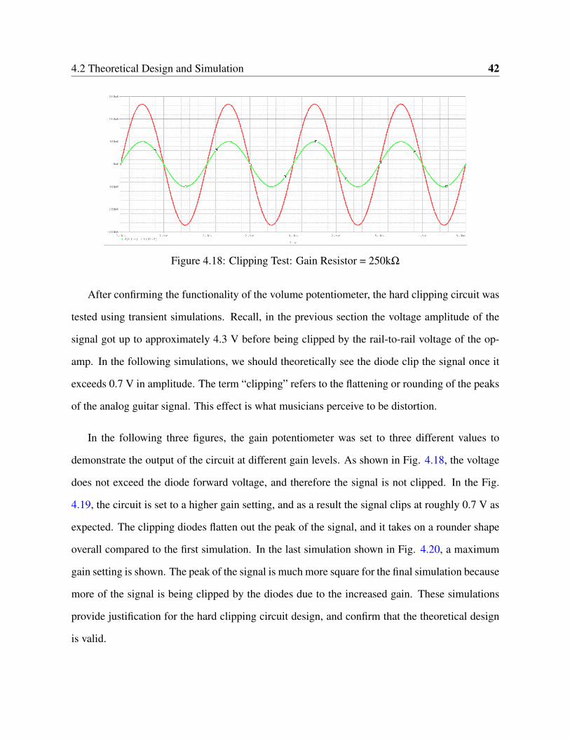
4.18 Clipping Test: Gain Resistor = 250kΩ . . . . . . . . . . . . . . . . . . . . . . . 42
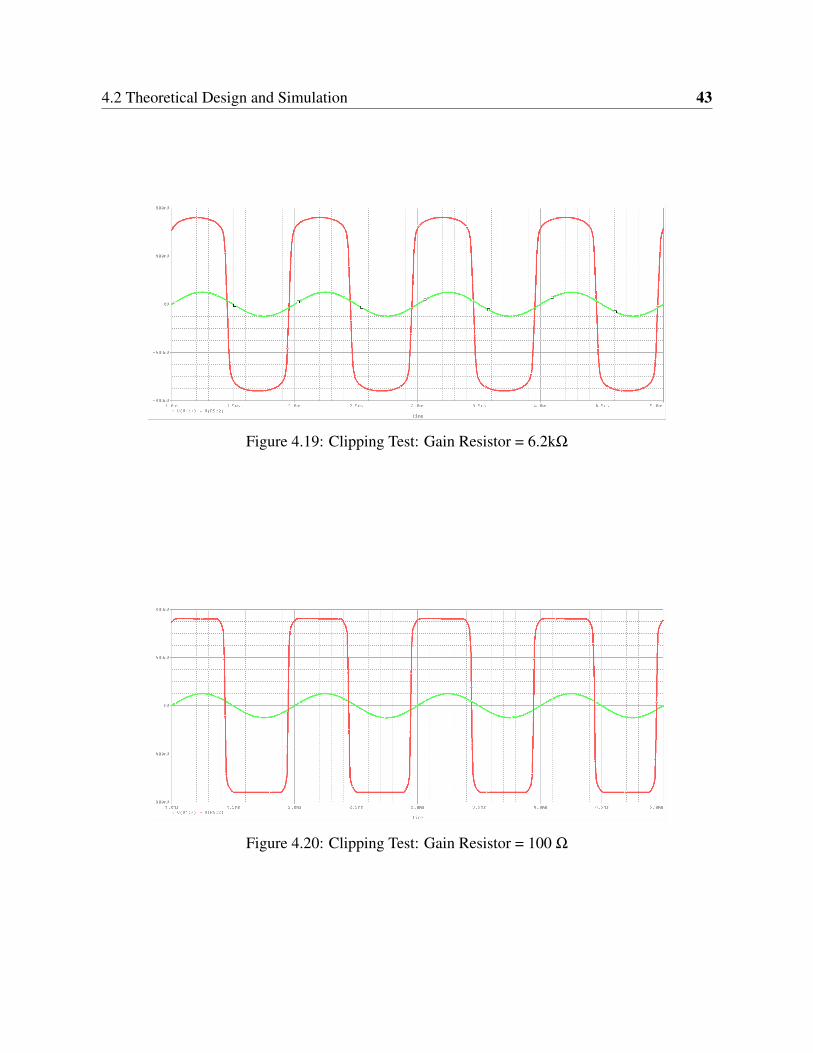
4.19 Clipping Test: Gain Resistor = 6.2kΩ . . . . . . . . . . . . . . . . . . . . . . . 43
4.20 Clipping Test: Gain Resistor = 100 Ω . . . . . . . . . . . . . . . . . . . . . . . 43
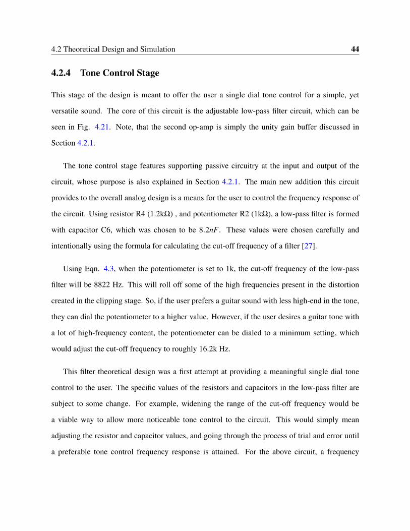
4.21 Tone Control Theoretical Schematic . . . . . . . . . . . . . . . . . . . . . . . . 45
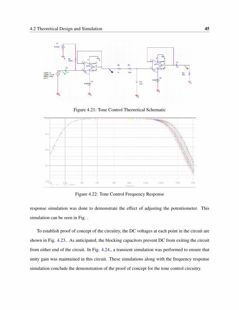
4.22 Tone Control Frequency Response . . . . . . . . . . . . . . . . . . . . . . . . . 45
4.23 Tone Control: DC Voltages . . . . . . . . . . . . . . . . . . . . . . . . . . . . . 46
4.24 Tone Control: Transient Simulation . . . . . . . . . . . . . . . . . . . . . . . . 46
4.25 Complete Theoretical Schematic . . . . . . . . . . . . . . . . . . . . . . . . . . 47
4.26 Transient 1: Gain potentiometer = 1MΩ . . . . . . . . . . . . . . . . . . . . . . 48
4.27 Transient 2: Gain potentiometer = 20kΩ . . . . . . . . . . . . . . . . . . . . . . 49
4.28 Transient 3: Gain potentiometer = 8kΩ . . . . . . . . . . . . . . . . . . . . . . 49
4.29 Frequency Response: Gain potentiometer = 1MΩ . . . . . . . . . . . . . . . . . 50
List of Figures x
4.30 Frequency Response: Gain potentiometer = 100kΩ . . . . . . . . . . . . . . . . 50
4.31 Frequency Response: Gain potentiometer = 10kΩ . . . . . . . . . . . . . . . . 51
5.1 Final Altium Schematic . . . . . . . . . . . . . . . . . . . . . . . . . . . . . . 54
5.2 Final PCB Layout . . . . . . . . . . . . . . . . . . . . . . . . . . . . . . . . . 56
5.3 Hardware Buffer Simulation . . . . . . . . . . . . . . . . . . . . . . . . . . . . 57
5.4 Hardware Gain Simulation: 1MΩ Potentiometer . . . . . . . . . . . . . . . . . 58
5.5 Hardware Gain Simulation: 10kΩ Potentiometer . . . . . . . . . . . . . . . . . 59
5.6 Hardware Gain Simulation: 4.7kΩ Potentiometer . . . . . . . . . . . . . . . . . 60
5.7 Hardware Tone Control Simulation . . . . . . . . . . . . . . . . . . . . . . . . . 61
5.8 Hardware Gain Simulation: 1MΩ Potentiometer . . . . . . . . . . . . . . . . . 63
5.9 Hardware Gain Simulation: 10kΩ Potentiometer . . . . . . . . . . . . . . . . . 64
5.10 Hardware Gain Simulation: 4.7kΩ Potentiometer . . . . . . . . . . . . . . . . . 65
5.11 Simulation of 1N4735 Diode . . . . . . . . . . . . . . . . . . . . . . . . . . . . 67
5.12 Simulation of 1N4148 Diode . . . . . . . . . . . . . . . . . . . . . . . . . . . . 68
5.13 Simulation of 1N914 Diode . . . . . . . . . . . . . . . . . . . . . . . . . . . . . 69
5.14 Simulation of 1N4004 Diode . . . . . . . . . . . . . . . . . . . . . . . . . . . . 70
5.15 Simulation of Red LED . . . . . . . . . . . . . . . . . . . . . . . . . . . . . . . 71
5.16 Simulation of 1N914 Diode . . . . . . . . . . . . . . . . . . . . . . . . . . . . . 73
5.17 Simulation of 1N4004 . . . . . . . . . . . . . . . . . . . . . . . . . . . . . . . 74
5.18 Simulation of Red LED . . . . . . . . . . . . . . . . . . . . . . . . . . . . . . 75
I.1 Ibanez Guitar Pedal . . . . . . . . . . . . . . . . . . . . . . . . . . . . . . . . . I-2
I.2 BOSS Guitar Pedal . . . . . . . . . . . . . . . . . . . . . . . . . . . . . . . . . I-3
I.3 Enclosure for Custom Analog pedal . . . . . . . . . . . . . . . . . . . . . . . . I-4
Chapter 1
Introduction
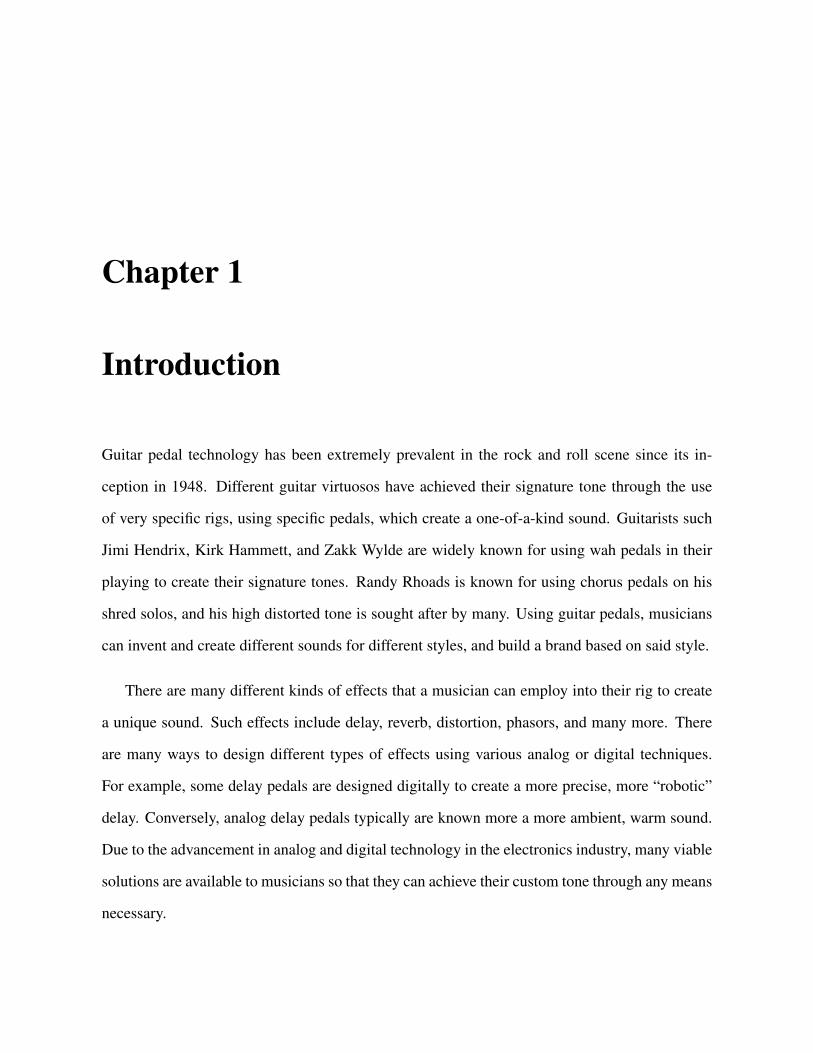
Guitar pedal technology has been extremely prevalent in the rock and roll scene since its in-
ception in 1948. Different guitar virtuosos have achieved their signature tone through the use
of very specific rigs, using specific pedals, which create a one-of-a-kind sound. Guitarists such
Jimi Hendrix, Kirk Hammett, and Zakk Wylde are widely known for using wah pedals in their
playing to create their signature tones. Randy Rhoads is known for using chorus pedals on his
shred solos, and his high distorted tone is sought after by many. Using guitar pedals, musicians
can invent and create different sounds for different styles, and build a brand based on said style.
There are many different kinds of effects that a musician can employ into their rig to create
a unique sound. Such effects include delay, reverb, distortion, phasors, and many more. There
are many ways to design different types of effects using various analog or digital techniques.
For example, some delay pedals are designed digitally to create a more precise, more “robotic”
delay. Conversely, analog delay pedals typically are known more a more ambient, warm sound.
Due to the advancement in analog and digital technology in the electronics industry, many viable
solutions are available to musicians so that they can achieve their custom tone through any means
necessary.
2
This paper specifically focuses on the design and theory revolving around analog distortion
circuitry. Analog circuitry offers many different advantages over digital technology. Analog
pedals are generally considered to sound more natural to most musicians, which is a preferable
trait for many musicians. Typically, even in amplifiers, analog circuitry is sought after due to its
natural, classic sound – which is why tube amplifiers have been, and will continue to dominate
the music industry. Similarly, analog distortion pedals aim to achieve a similar natural yet classic
tone made famous by vintage amplifiers during the 70’s and 80’s.
1.0.1 Research Goals
During this research project, the main goal is to better understand the theory and design involved
in creating a custom distortion pedal. Doing this project will help provide the necessary experi-
ence needed to be successful not only at RIT, but also as an practicing engineer. Ultimately, the
research and design process used throughout this project will build a foundation of knowledge
essential to being a professional audio-electrical engineer. Listed below are several main points
the scope of this project aims to cover.
• To understand how various distortion types of distortion circuits function (operational am-
plifier circuits, transistor circuits, etc)
• To understand how different diodes can perform different types of clipping, and why cer-
tain diodes perform differently than others
• To design an effective but simple distortion pedal that provides the user with versatility,
and reliability, with a satisfying distorted sound
3
1.0.2 Contributions
The significant contributions to the projected are as follows:
1. An input buffer circuit with high input resistance, and low output resistance
2. A distortion circuit with specifically sculpted tonal characteristics to create a “custom”
distortion
3. An analysis of different diode characteristics and performance
4. Tone control circuit
5. Volume control circuit
6. Mathematical and logical justification using appropriate analog design theory and PSPICE
analysis
1.0.3 Organization
The structure of the paper is as follows:
• Chapter 2: This chapter discusses background information and literature sources related
to electric guitar, music, and basic concepts related to electrical applications in the music
industry.
• Chapter 3: This chapter aims to discuss the general implementation of a guitar distortion
pedal circuit. The overall design is divided into smaller subsections and discussed in detail.
• Chapter 4: This chapter delves into the specifics of the theoretical designs, the expected
performance, and relevant theoretical simulations in PSPICE.
4
• Chapter 5: This chapter mainly focuses on the hardware application of the theoretical
design, and the testing of the hardware implementation.
• Chapter 6: This chapter presents a summary of results and final conclusions.
• Appendix: This section includes relevant snapshots of some common guitar pedals
Chapter 2
Related Work
2.1 Introduction
This chapter aims to discuss background information about the history of electric guitars, and
related work that has contributed to the development of musical engineering technologies and
innovations. The following sections will present some important concepts in understanding the
electric guitar, and its role in the music industry. Additionally, an explanation on how musical
technologies have impacted the electric guitar, and the music industry will be touched on. It is
important to understand the electric guitar’s role in music, and its associated technologies because
these technologies interact with each other in a very specific manner. Therefore, knowing the
mathematics and theory behind these technologies will be useful when designing any type of
guitar pedal.
2.2 A Brief History of the Electric Guitar 6
2.2 A Brief History of the Electric Guitar
Before the invention of the electric guitar, musicians had already been playing acoustic guitar
professionally for hundreds of years. Typically, the instrument was used in smaller ensembles,
or performed solo, and it was generally for smaller scale performances. However, because of its
quiet nature, it was not suitable for larger ensembles or bands. In larger ensembles, the guitar
was typically unable to achieve volume levels easily achieved by other woodwind and brass
instruments. Until the conception of the electric guitar and powered speakers, there was no way
to combat this issue.
The electric guitar is an instrument that brought something to the music industry that the
world had never seen before. Not only did it provide a means for a guitarist to attain higher
volumes, but it would provide a whole new flavor of tonal options that the acoustic guitar was
unable to offer. Because of this, the electric guitar was an invention that would revolutionize the
music industry in the coming decades like no other instrument had ever before.
In the 1950’s, rock and blues music began to take over the music industry, and it was be-
coming a sensation that was sweeping the United States, and the rest of the modern world. As
technologies continued to advance, new sounds continued to emerge. Suddenly, guitar virtuoso
players such as Jimi Hendrix, Eddie Van Halen, and Jimmy Page were blasting distorted rock
guitar riffs and solos, made possible by tube amplifiers and guitar pedal effects. With the help
of classic tube amplifiers and an abundance of emerging guitar pedal technologies, the electric
guitar was able to evolve into an instrument that filled a niche in the music industry that no other
instrument could imitate. As a result, we now remember the 70’s and 80’s as the decades of
classic rock.
2.3 The Electric Guitar: Elementary Concepts 7
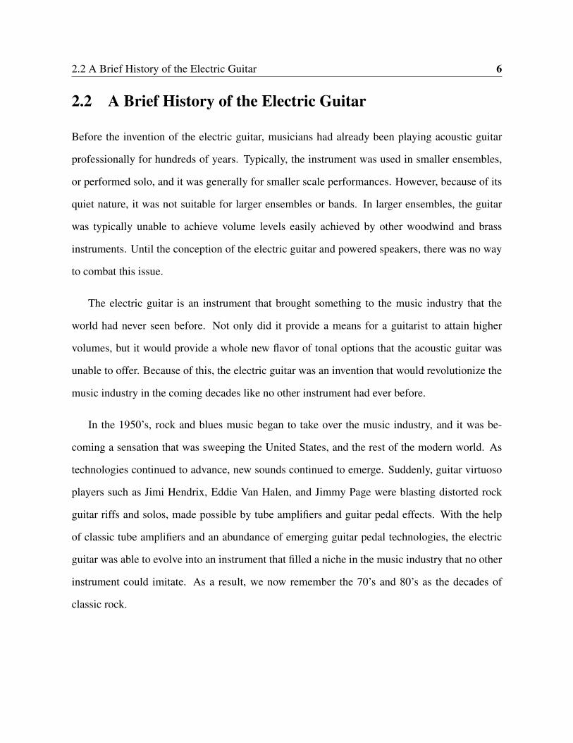
Figure 2.1: Single Coil Guitar Pickup [1]
2.3 The Electric Guitar: Elementary Concepts
2.3.1 Magnetic Guitar Pickups
The electric guitar is an instrument that uses magnetic pickups to sense vibrations made by the
strings on the guitar. The theory and background of how a pickup works is discussed in detail in
[1, 2, 7? ]. Essentially, a guitar pickup is made of several magnets, wound with copper wire. A
guitar pickup has an inherent magnetic field associated with it created by the permanent magnets.
When a guitar string vibrates, it creates a disturbance in the magnetic field of the pickup. This
induces a voltage onto the pickups which mathematically represents the sound being produced
by the string. This signal is what defines the sound of an electric guitar. In [8] the mechanics
of how a guitar string vibrates are discussed, and mathematical modeling of real world analog
sound is demonstrated. Shown in Fig. 2.1 [1], is a standard single coil guitar pick up 3D model.
We can describe the behavior of a guitar pickup using the Faraday-Lenz laws of physics
[1]. The flux of a magnetic field can be described as the integral in Eqn. 2.1. B represents the
magnetic field at a given point in time for a permanent magnet, and dS is the surface represented
by the magnetic single coil pickup.
2.3 The Electric Guitar: Elementary Concepts 8
Φ =∫∫
B(t)•dS (2.1)
When a guitar string vibrates, it alters the magnetic field emitted by the pickup, which
changes the flux across the coil. Faraday’s law states that the negative change in flux will in-
duce a voltage onto the coils of the guitar pickup. This voltage induced is the signal that gets
input to a guitar amplifier, and output by the speakers.
u(t) =−dΦ
dt(2.2)
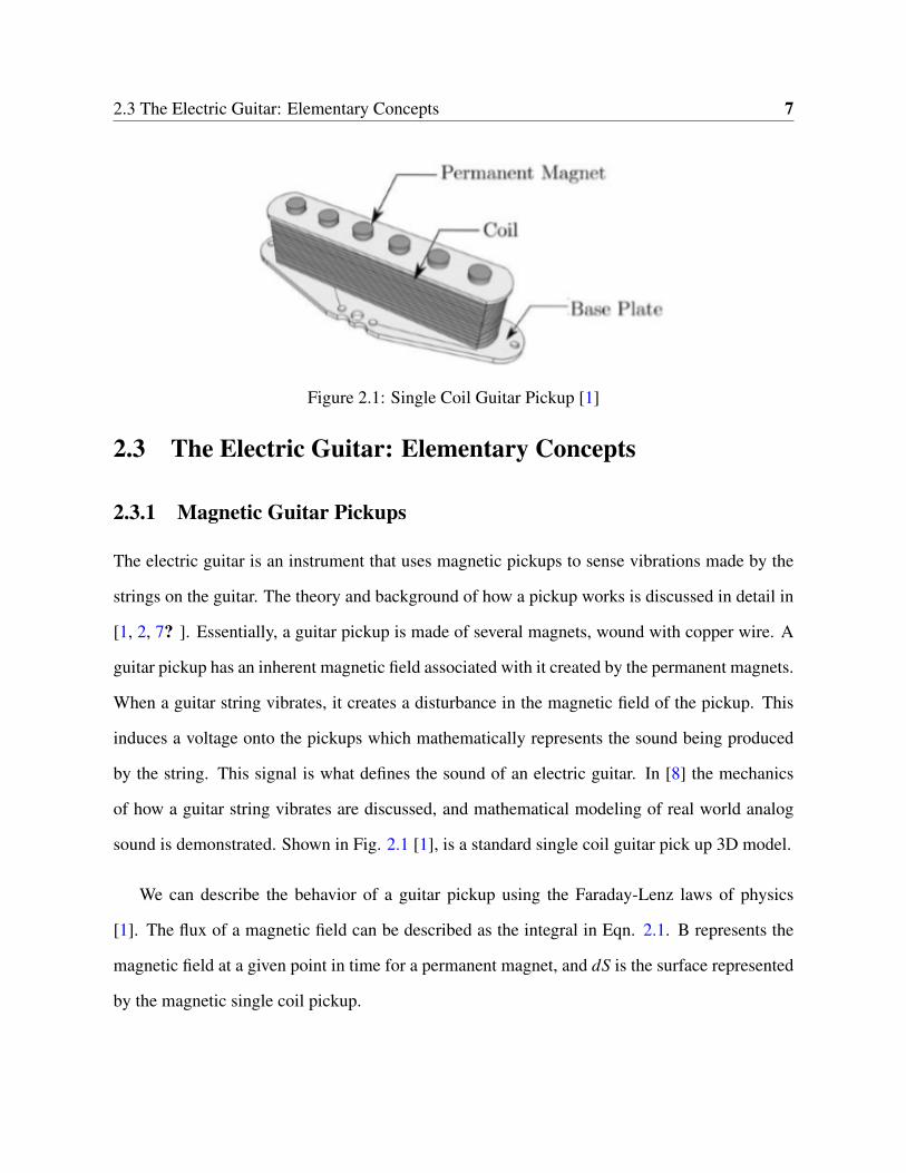
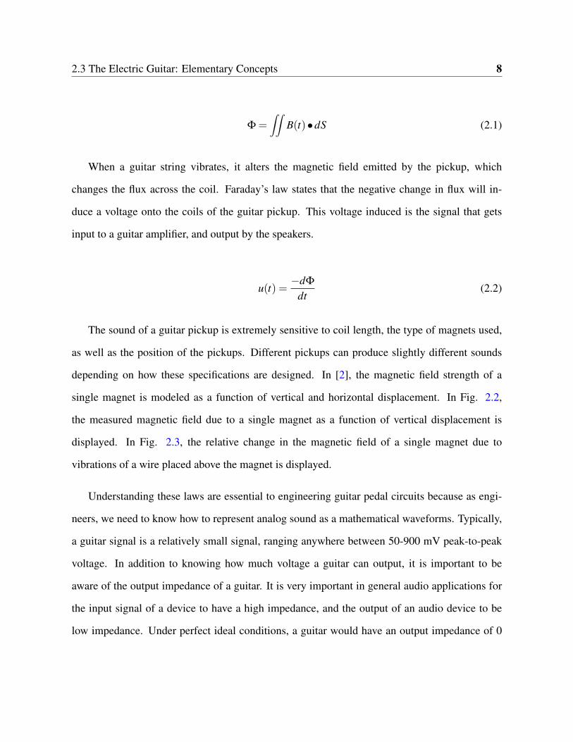
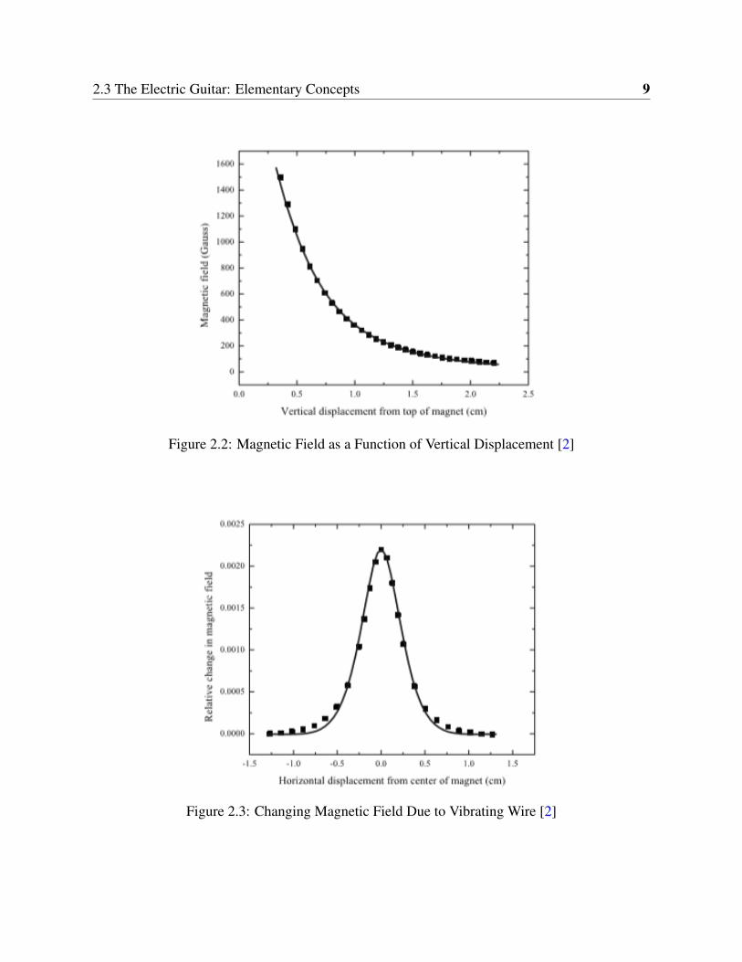
The sound of a guitar pickup is extremely sensitive to coil length, the type of magnets used,
as well as the position of the pickups. Different pickups can produce slightly different sounds
depending on how these specifications are designed. In [2], the magnetic field strength of a
single magnet is modeled as a function of vertical and horizontal displacement. In Fig. 2.2,
the measured magnetic field due to a single magnet as a function of vertical displacement is
displayed. In Fig. 2.3, the relative change in the magnetic field of a single magnet due to
vibrations of a wire placed above the magnet is displayed.
Understanding these laws are essential to engineering guitar pedal circuits because as engi-
neers, we need to know how to represent analog sound as a mathematical waveforms. Typically,
a guitar signal is a relatively small signal, ranging anywhere between 50-900 mV peak-to-peak
voltage. In addition to knowing how much voltage a guitar can output, it is important to be
aware of the output impedance of a guitar. It is very important in general audio applications for
the input signal of a device to have a high impedance, and the output of an audio device to be
low impedance. Under perfect ideal conditions, a guitar would have an output impedance of 0
2.3 The Electric Guitar: Elementary Concepts 9
Figure 2.2: Magnetic Field as a Function of Vertical Displacement [2]
Figure 2.3: Changing Magnetic Field Due to Vibrating Wire [2]
2.3 The Electric Guitar: Elementary Concepts 10
ohms, which would enable an 100% efficient signal transfer. However, due to the impedance of
the pickups and internal circuitry, a guitar typically has an output impedance of around 5k-15k
ohms[9]. All of these factors and specifications must be taken into account when designing a
guitar effects pedal.
2.3.2 Guitar Amplifiers: Valve vs Solid State
The guitar industry offers a wide range of different kinds of amplifiers for the practicing musi-
cian. There are two main types of amplifiers primarily used by guitarists: Valve amplifiers , and
solid-state amplifiers. Valve amplifiers [3, 4, 10] are a type of amplifier that use vacuum tubes to
amplify and distort a signal. Many guitarists prefer this type of amplifier for its “classic” sound,
made popular by bands like AC/DC, Guns n’ Roses, Van Halen, and many more. However, due
to their large size, and high power requirements, guitar pedals and solid-state amplifiers stray
away from using tubes to create distortion, in favor of using transistor circuits to create gain
[11–13]. These amplifiers tend to have very different tonal characteristics from tube amplifiers.
Tube amplifiers are known for having a more natural, warm sound, while solid-state amplifiers
are known for having pure cleans and more harsh distortions. In [14], a digital model of a the
sound of a tube amplifier is modeled, and discusses the non-linearity associated with distortion.
Both types of amplifiers offer a different set of advantages and disadvantages. Solid state
amplifiers tend to be cheaper, and much lighter, which makes them easier to take to performances.
Solid state amplifiers also usually don’t require much maintenance, and typically have a very long
life cycle. Because of the nature of how vacuum tubes function, they can often crack, break, or
just burn out from long periods of use, and thus often need replacing. However, while being more
fragile, they usually offer a more versatile distortion than a solid state amplifier. There are certain
types of distortions you cannot produce with a solid state amplifier that a tube amplifier can offer.
2.3 The Electric Guitar: Elementary Concepts 11
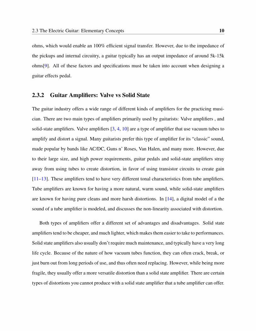
Figure 2.4: Valve vs Solid State Frequency Response [3]
Tonal differences between the two types of amplifiers are talked about in [3, 4]. Although these
differences can be subtle to the untrained ear, they can make all the difference to a professional
musician.
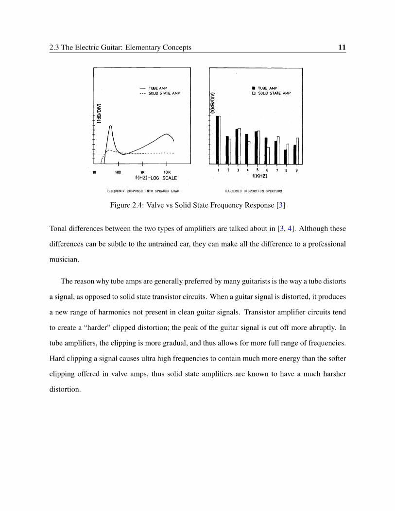
The reason why tube amps are generally preferred by many guitarists is the way a tube distorts
a signal, as opposed to solid state transistor circuits. When a guitar signal is distorted, it produces
a new range of harmonics not present in clean guitar signals. Transistor amplifier circuits tend
to create a “harder” clipped distortion; the peak of the guitar signal is cut off more abruptly. In
tube amplifiers, the clipping is more gradual, and thus allows for more full range of frequencies.
Hard clipping a signal causes ultra high frequencies to contain much more energy than the softer
clipping offered in valve amps, thus solid state amplifiers are known to have a much harsher
distortion.
2.3 The Electric Guitar: Elementary Concepts 12
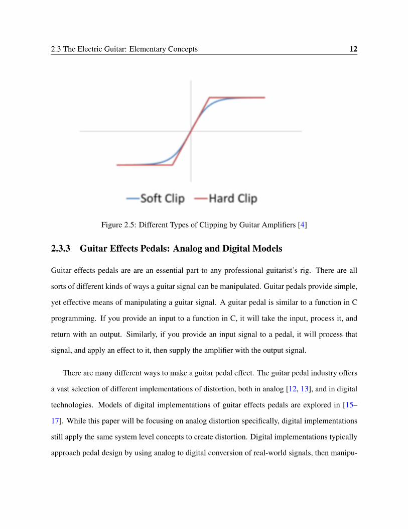
Figure 2.5: Different Types of Clipping by Guitar Amplifiers [4]
2.3.3 Guitar Effects Pedals: Analog and Digital Models
Guitar effects pedals are are an essential part to any professional guitarist’s rig. There are all
sorts of different kinds of ways a guitar signal can be manipulated. Guitar pedals provide simple,
yet effective means of manipulating a guitar signal. A guitar pedal is similar to a function in C
programming. If you provide an input to a function in C, it will take the input, process it, and
return with an output. Similarly, if you provide an input signal to a pedal, it will process that
signal, and apply an effect to it, then supply the amplifier with the output signal.
There are many different ways to make a guitar pedal effect. The guitar pedal industry offers
a vast selection of different implementations of distortion, both in analog [12, 13], and in digital
technologies. Models of digital implementations of guitar effects pedals are explored in [15–
17]. While this paper will be focusing on analog distortion specifically, digital implementations
still apply the same system level concepts to create distortion. Digital implementations typically
approach pedal design by using analog to digital conversion of real-world signals, then manipu-
2.3 The Electric Guitar: Elementary Concepts 13
lating the sampled signal using programming algorithms [17]. In analog design, the manipulation
of the signal is done using a combination of transistor and operational amplifier circuits [12, 13].
In most situations, analog pedals rule the market, as the sound quality of such designs are of-
ten preferred by most musicians. Analog circuitry is simply just more suitable to deliver what hu-
mans perceive to be natural, while digital implementations offer more clean-cut, robotic sounds.
For example, one of the more popular delay pedals used by many guitarists today is the MXR
Carbon Copy delay. This delay provides a more ambient, muddy delay. Whereas, a digital imple-
mentation such as the BOSS DD-8 creates nearly an exact replica of a given input signal, and just
offsets the delivery time using linear system theory of the sampling of a signal. However, both
pedals have their place in the market, as they can both provide different sound models that can
be appropriate for different situations. The modeling of certain nonlinear guitar effects pedals is
talked about in [18, 19].
2.3.4 Creating Distortion and Overdrive
Overdrive and distortion is an essential effect to have for most professional blues or rock mu-
sicians. In the formative years of rock music and the electric guitar, overdrive and distortion
was commonly created by over-driving vacuum tubes which would clip the signal, creating a
distorted sound. This sound was made famous by bands like the Rolling Stones, Led Zeppelin,
and Black Sabbath. Back then, analog circuitry dominated the industry when it came to creating
distortion pedals, and amplifiers. Today, there are some other modern digital applications avail-
able, but analog circuitry still dominates the industry because of its signature tone. In [20], some
numerical analysis and mathematical models are presented for distortion.
Analog circuitry creates distortion and overdrive primarily using some combination of tran-
2.3 The Electric Guitar: Elementary Concepts 14
sistors, operational amplifiers [12, 21], and diodes. Distortion is the result of a sound wave being
clipped at the peaks of a given waveform. Thus, because of this clipping of the signal, distortion
is a non-linear effect. Typically, in guitar pedal applications, the clipping is done by limiting
diodes. Recall, that diodes are a type of component that can limit current flow in a specific direc-
tion. Hence, when placed at the output of a gain amplifier, they are able to clip the signal when
that signal is greater than or equal to the forward voltage of the diode. The type of diode, and
placement of the diode is critical in the formation of the sound and tone of the distortion. If the
diodes are placed in the feedback path of a gain amplifier circuit, it can create a softer distor-
tion, classified in the music industry as overdrive [22]. When the clipping diodes are placed at
the output of a gain amplifier, it creates a hard clipping effect, known as distortion in the music
industry. However, overdrive and distortion are used interchangeably in casual conversation.
Some very popular distortion pedals in the industry include the Ibanez tube screamer TS-9,
and the BOSS DS-1. Real time modeling of these circuits is done in [23]. Both of these con-
figurations use non-inverting operational amplifiers to apply gain to the input signal. Displayed
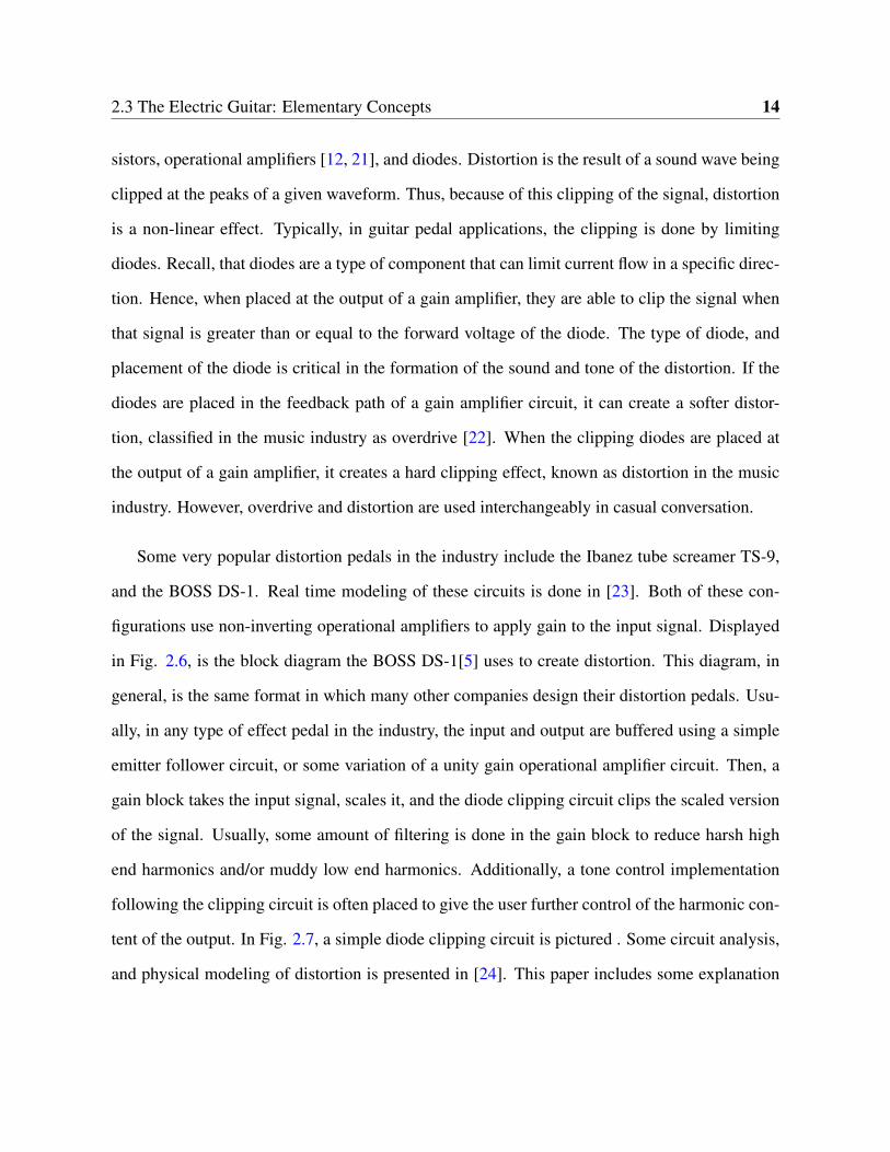
in Fig. 2.6, is the block diagram the BOSS DS-1[5] uses to create distortion. This diagram, in
general, is the same format in which many other companies design their distortion pedals. Usu-
ally, in any type of effect pedal in the industry, the input and output are buffered using a simple
emitter follower circuit, or some variation of a unity gain operational amplifier circuit. Then, a
gain block takes the input signal, scales it, and the diode clipping circuit clips the scaled version
of the signal. Usually, some amount of filtering is done in the gain block to reduce harsh high
end harmonics and/or muddy low end harmonics. Additionally, a tone control implementation
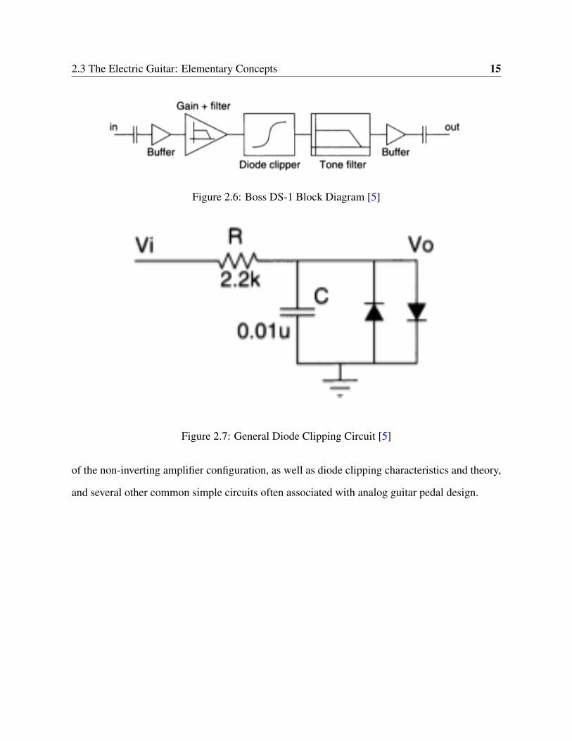
following the clipping circuit is often placed to give the user further control of the harmonic con-
tent of the output. In Fig. 2.7, a simple diode clipping circuit is pictured . Some circuit analysis,
and physical modeling of distortion is presented in [24]. This paper includes some explanation
2.3 The Electric Guitar: Elementary Concepts 15
Figure 2.6: Boss DS-1 Block Diagram [5]
Figure 2.7: General Diode Clipping Circuit [5]
of the non-inverting amplifier configuration, as well as diode clipping characteristics and theory,
and several other common simple circuits often associated with analog guitar pedal design.
Chapter 3
Architecture and Implementation of Design
3.1 Block Diagram Overview
This portion of the paper outlines the high-level block diagram design of the system. Each section
of this chapter covers each of the low-level blocks which make up the overall design. The block
diagram begins with a buffer circuit block, followed by a gain block, a hard clipping stage, a tone
control block, and finally an output buffer circuit. This basic block diagram is a very common
configuration that many analog distortion pedals use in the industry today [5, 23].
3.1.1 Top Level Block Diagram
Shown below in Fig. 3.1 is the top level block diagram of the system. This section is meant to
give a brief summary of each block in the system. Each block performs one specific task which
is required for the overall system to function. The power block provides the integrated circuits
in the system with a 9 V power source, as well as providing a 4.5 V virtual ground reference.
The input buffer circuit allows for accurate and complete transferal of the input signal to the
gain stage, and prevents any loss of signal. The gain stage takes the given input signal from the
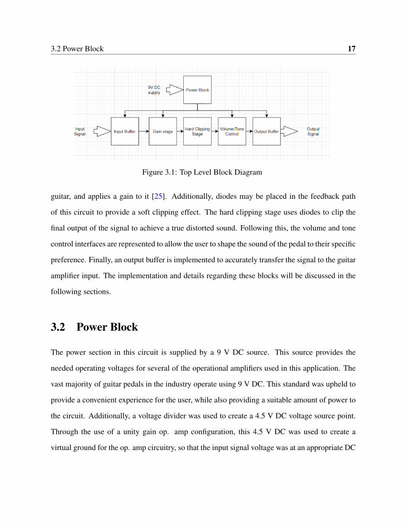
3.2 Power Block 17
Figure 3.1: Top Level Block Diagram
guitar, and applies a gain to it [25]. Additionally, diodes may be placed in the feedback path
of this circuit to provide a soft clipping effect. The hard clipping stage uses diodes to clip the
final output of the signal to achieve a true distorted sound. Following this, the volume and tone
control interfaces are represented to allow the user to shape the sound of the pedal to their specific
preference. Finally, an output buffer is implemented to accurately transfer the signal to the guitar
amplifier input. The implementation and details regarding these blocks will be discussed in the
following sections.
3.2 Power Block
The power section in this circuit is supplied by a 9 V DC source. This source provides the
needed operating voltages for several of the operational amplifiers used in this application. The
vast majority of guitar pedals in the industry operate using 9 V DC. This standard was upheld to
provide a convenient experience for the user, while also providing a suitable amount of power to
the circuit. Additionally, a voltage divider was used to create a 4.5 V DC voltage source point.
Through the use of a unity gain op. amp configuration, this 4.5 V DC was used to create a
virtual ground for the op. amp circuitry, so that the input signal voltage was at an appropriate DC
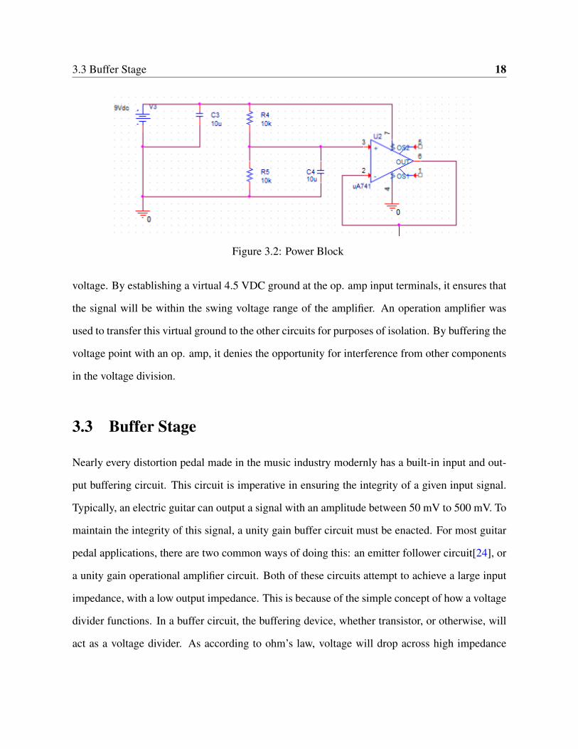
3.3 Buffer Stage 18
Figure 3.2: Power Block
voltage. By establishing a virtual 4.5 VDC ground at the op. amp input terminals, it ensures that
the signal will be within the swing voltage range of the amplifier. An operation amplifier was
used to transfer this virtual ground to the other circuits for purposes of isolation. By buffering the
voltage point with an op. amp, it denies the opportunity for interference from other components
in the voltage division.
3.3 Buffer Stage
Nearly every distortion pedal made in the music industry modernly has a built-in input and out-
put buffering circuit. This circuit is imperative in ensuring the integrity of a given input signal.
Typically, an electric guitar can output a signal with an amplitude between 50 mV to 500 mV. To
maintain the integrity of this signal, a unity gain buffer circuit must be enacted. For most guitar
pedal applications, there are two common ways of doing this: an emitter follower circuit[24], or
a unity gain operational amplifier circuit. Both of these circuits attempt to achieve a large input
impedance, with a low output impedance. This is because of the simple concept of how a voltage
divider functions. In a buffer circuit, the buffering device, whether transistor, or otherwise, will
act as a voltage divider. As according to ohm’s law, voltage will drop across high impedance
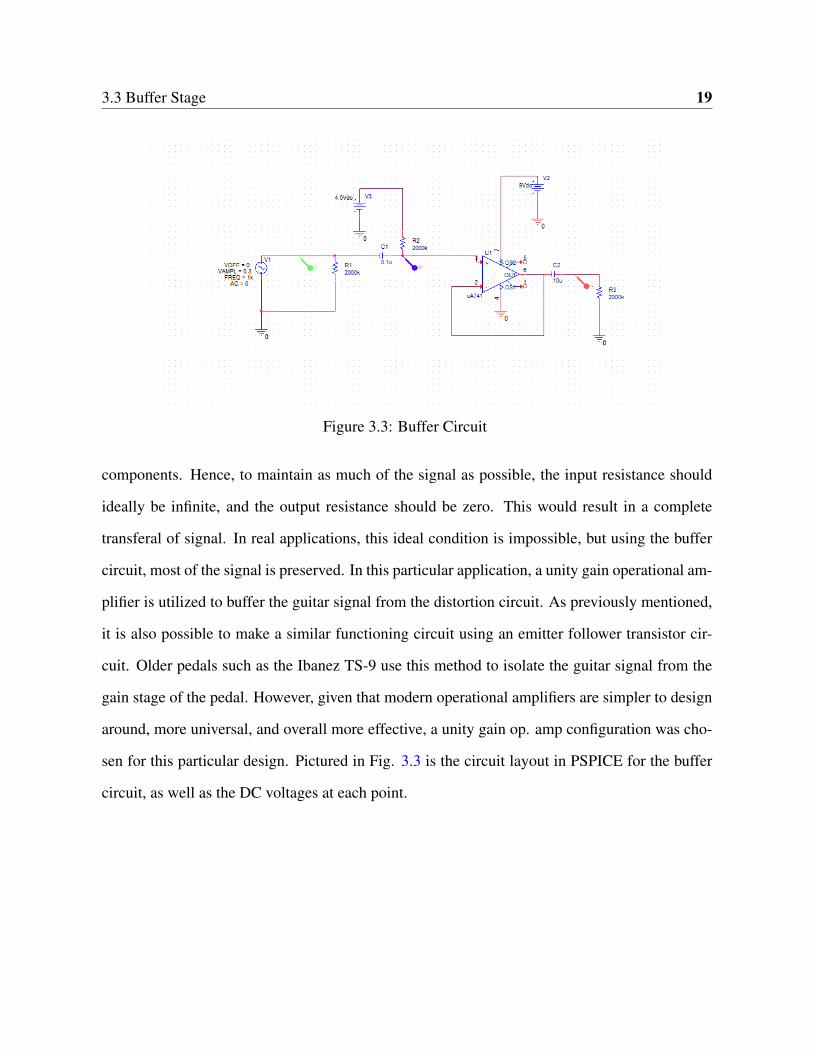
3.3 Buffer Stage 19
Figure 3.3: Buffer Circuit
components. Hence, to maintain as much of the signal as possible, the input resistance should
ideally be infinite, and the output resistance should be zero. This would result in a complete
transferal of signal. In real applications, this ideal condition is impossible, but using the buffer
circuit, most of the signal is preserved. In this particular application, a unity gain operational am-
plifier is utilized to buffer the guitar signal from the distortion circuit. As previously mentioned,
it is also possible to make a similar functioning circuit using an emitter follower transistor cir-
cuit. Older pedals such as the Ibanez TS-9 use this method to isolate the guitar signal from the
gain stage of the pedal. However, given that modern operational amplifiers are simpler to design
around, more universal, and overall more effective, a unity gain op. amp configuration was cho-
sen for this particular design. Pictured in Fig. 3.3 is the circuit layout in PSPICE for the buffer
circuit, as well as the DC voltages at each point.
3.4 Gain Stage 20
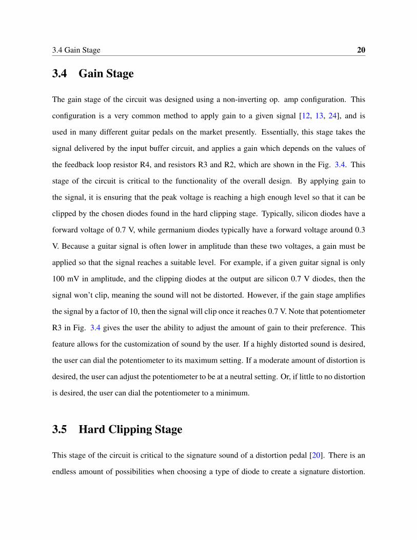
3.4 Gain Stage
The gain stage of the circuit was designed using a non-inverting op. amp configuration. This
configuration is a very common method to apply gain to a given signal [12, 13, 24], and is
used in many different guitar pedals on the market presently. Essentially, this stage takes the
signal delivered by the input buffer circuit, and applies a gain which depends on the values of
the feedback loop resistor R4, and resistors R3 and R2, which are shown in the Fig. 3.4. This
stage of the circuit is critical to the functionality of the overall design. By applying gain to
the signal, it is ensuring that the peak voltage is reaching a high enough level so that it can be
clipped by the chosen diodes found in the hard clipping stage. Typically, silicon diodes have a
forward voltage of 0.7 V, while germanium diodes typically have a forward voltage around 0.3
V. Because a guitar signal is often lower in amplitude than these two voltages, a gain must be
applied so that the signal reaches a suitable level. For example, if a given guitar signal is only
100 mV in amplitude, and the clipping diodes at the output are silicon 0.7 V diodes, then the
signal won’t clip, meaning the sound will not be distorted. However, if the gain stage amplifies
the signal by a factor of 10, then the signal will clip once it reaches 0.7 V. Note that potentiometer
R3 in Fig. 3.4 gives the user the ability to adjust the amount of gain to their preference. This
feature allows for the customization of sound by the user. If a highly distorted sound is desired,
the user can dial the potentiometer to its maximum setting. If a moderate amount of distortion is
desired, the user can adjust the potentiometer to be at a neutral setting. Or, if little to no distortion
is desired, the user can dial the potentiometer to a minimum.
3.5 Hard Clipping Stage
This stage of the circuit is critical to the signature sound of a distortion pedal [20]. There is an
endless amount of possibilities when choosing a type of diode to create a signature distortion.
3.5 Hard Clipping Stage 21
Figure 3.4: Non-inverting Amplifier: Gain Stage
Recall that a diode is a component that only allows current to flow in one direction. This funda-
mental concept allows the incoming guitar signal to be clipped at the output, creating a distorted
guitar sound. In the music industry, many different pedals use different kinds of diodes to get a
different signature sound. The type of diodes used depend on the preference of the designer, or
user of the pedal. In this paper, several different diodes are explored and tested to determine the
effects different diodes can have on the sound and frequency response of the circuit. In terms of
function, the clipping stage does not depend on the type of diode used, except that the forward
voltage can vary between different types of diodes. In terms of sound definition and tone, the
type of diode is key in defining the characteristics of the sound. Some diodes can produce a more
muddy sound, while others may deliver a more precise sound. In this paper, several different
types of diodes are examined and modeled to show the difference in sound quality that certain
diodes can offer compared to others. Often times, these differences can be subtle, but any small
difference can mean a lot to the attuned ear of a practicing musician. In the world of music, a
small tonal difference can make or break a song, or even an entire album. Hence, knowing which
3.5 Hard Clipping Stage 22
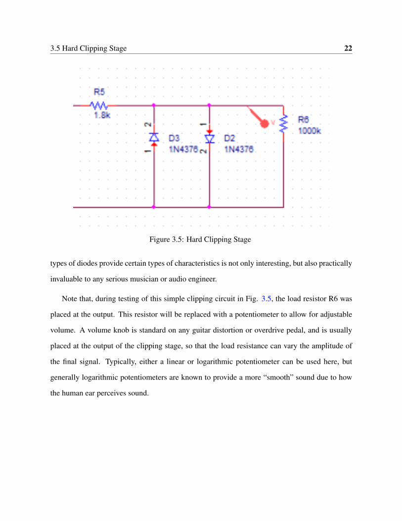
Figure 3.5: Hard Clipping Stage
types of diodes provide certain types of characteristics is not only interesting, but also practically
invaluable to any serious musician or audio engineer.
Note that, during testing of this simple clipping circuit in Fig. 3.5, the load resistor R6 was
placed at the output. This resistor will be replaced with a potentiometer to allow for adjustable
volume. A volume knob is standard on any guitar distortion or overdrive pedal, and is usually
placed at the output of the clipping stage, so that the load resistance can vary the amplitude of
the final signal. Typically, either a linear or logarithmic potentiometer can be used here, but
generally logarithmic potentiometers are known to provide a more “smooth” sound due to how
the human ear perceives sound.
3.6 Tone Control Stage 23
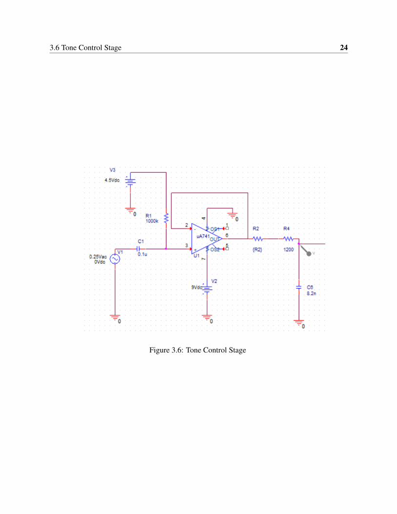
3.6 Tone Control Stage
In addition to the hard clipping stage, the tone control stage is yet another way a distortion pedal
can create its own signature sounds. This stage provides a lot of creative freedom to the designer,
as it allows for sculpting of the frequency response of the signal. Many pedals in the industry
have 3 separate equalization dials: treble, mid, and bass. Others have just one master tone control
for simplicity and ease. These circuits, while very powerful and useful, are also actually no more
than simple RC filtering circuits. Using RC filter circuits such as low-pass, high-pass, band-pass,
and band-reject filters, a design engineer can mathematically place desired cutoff frequencies
along the frequency range to achieve a desired tonal signature. In this application, an operational
amplifier low pass filter circuit is used as a master tone control to allow for versatile but simple
tonal control. This low-pass filter is comprised of resistors R2 and R4, as well the capacitor C6.
The low-pass filter was placed at the output of the op. amp for isolation purposes. The way this
circuit functions is actually quite simple; the potentiometer allows the cut off frequency to be
adjusted as preferred by the user. The higher the value of the potentiometer, the lower the cutoff
frequency. So if the user were to prefer to have a lot of treble and presence, then they could
adjust the potentiometer to a lower setting. If the user preferred less prominent high frequencies
in their tone, they could adjust the potentiometer to a higher position. Pictured below in Fig. 3.6
is the tone control op. amp circuit design.
3.6 Tone Control Stage 24
Figure 3.6: Tone Control Stage
Chapter 4
Theoretical Analysis and Design
In this section of the paper, the aim is to go over in detail all of the mathematics and theory
involved in the design process of an analog distortion pedal. Additionally, the material presented
in this section will offer explanation and justification for specific design decisions made for the
analog circuitry. Lastly, a proof of concept will be established in the theoretical simulations
provided, which will provide a logical expectation for the performance of the design, and its
characteristics.
4.1 Fundamental Theoretical Concepts
4.1.1 Operational Amplifiers
Modernly, most analog distortion pedals are created using cascaded operational amplifiers cou-
pled with supporting passive circuitry. Operational amplifiers are an active linear component that
can be used to create gain in a circuit, which is essential in the case of creating distortion. The
operational amplifier is a very universal in nature; it can be used for a wide range of applications
including but not limited to signal conditioning, active filters, and mathematical operations. Be-
4.1 Fundamental Theoretical Concepts 26
cause of its nearly ideal operating conditions, it has become an industry staple for analog guitar
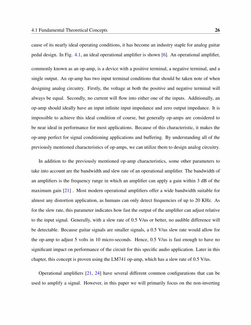
pedal design. In Fig. 4.1, an ideal operational amplifier is shown [6]. An operational amplifier,
commonly known as an op-amp, is a device with a positive terminal, a negative terminal, and a
single output. An op-amp has two input terminal conditions that should be taken note of when
designing analog circuitry. Firstly, the voltage at both the positive and negative terminal will
always be equal. Secondly, no current will flow into either one of the inputs. Additionally, an
op-amp should ideally have an input infinite input impedance and zero output impedance. It is
impossible to achieve this ideal condition of course, but generally op-amps are considered to
be near ideal in performance for most applications. Because of this characteristic, it makes the
op-amp perfect for signal conditioning applications and buffering. By understanding all of the
previously mentioned characteristics of op-amps, we can utilize them to design analog circuitry.
In addition to the previously mentioned op-amp characteristics, some other parameters to
take into account are the bandwidth and slew rate of an operational amplifier. The bandwidth of
an amplifiers is the frequency range in which an amplifier can apply a gain within 3 dB of the
maximum gain [21] . Most modern operational amplifiers offer a wide bandwidth suitable for
almost any distortion application, as humans can only detect frequencies of up to 20 KHz. As
for the slew rate, this parameter indicates how fast the output of the amplifier can adjust relative
to the input signal. Generally, with a slew rate of 0.5 V/us or better, no audible difference will
be detectable. Because guitar signals are smaller signals, a 0.5 V/us slew rate would allow for
the op-amp to adjust 5 volts in 10 micro-seconds. Hence, 0.5 V/us is fast enough to have no
significant impact on performance of the circuit for this specific audio application. Later in this
chapter, this concept is proven using the LM741 op-amp, which has a slew rate of 0.5 V/us.
Operational amplifiers [21, 24] have several different common configurations that can be
used to amplify a signal. However, in this paper we will primarily focus on the non-inverting
4.1 Fundamental Theoretical Concepts 27
Figure 4.1: Ideal Operational Amplifier [6]
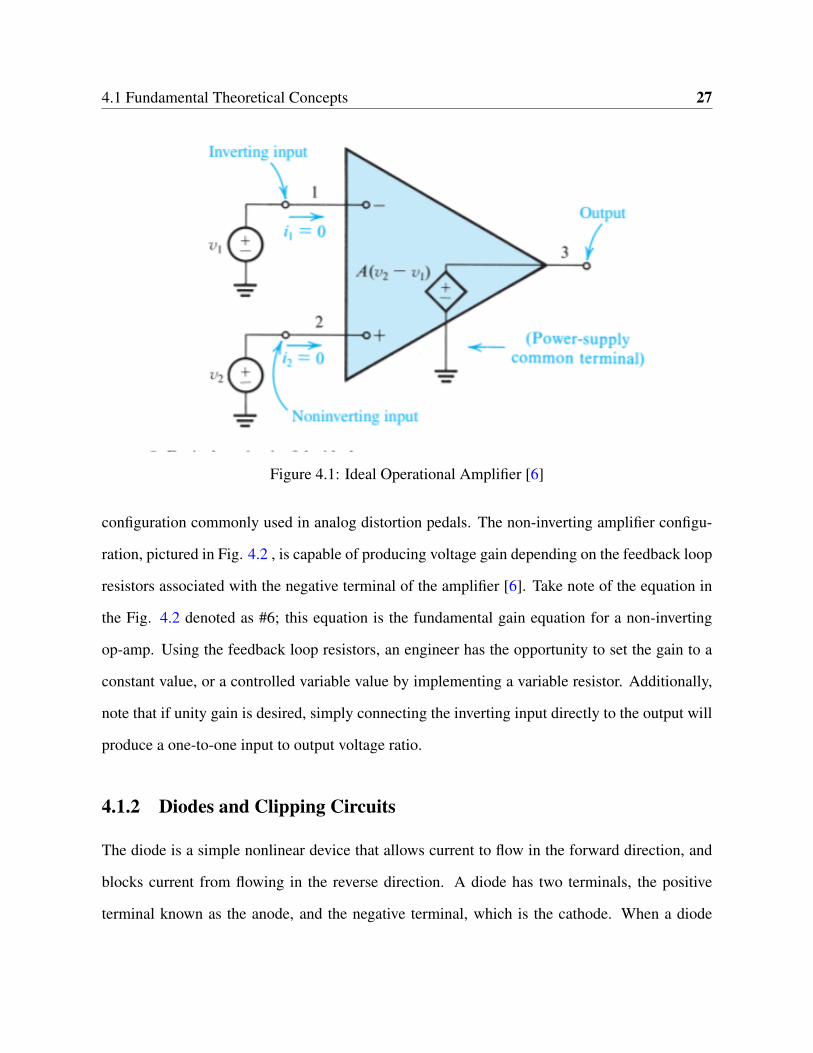
configuration commonly used in analog distortion pedals. The non-inverting amplifier configu-
ration, pictured in Fig. 4.2 , is capable of producing voltage gain depending on the feedback loop
resistors associated with the negative terminal of the amplifier [6]. Take note of the equation in
the Fig. 4.2 denoted as #6; this equation is the fundamental gain equation for a non-inverting
op-amp. Using the feedback loop resistors, an engineer has the opportunity to set the gain to a
constant value, or a controlled variable value by implementing a variable resistor. Additionally,
note that if unity gain is desired, simply connecting the inverting input directly to the output will
produce a one-to-one input to output voltage ratio.
4.1.2 Diodes and Clipping Circuits
The diode is a simple nonlinear device that allows current to flow in the forward direction, and
blocks current from flowing in the reverse direction. A diode has two terminals, the positive
terminal known as the anode, and the negative terminal, which is the cathode. When a diode
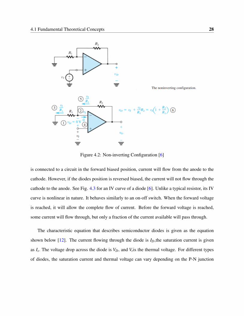
4.1 Fundamental Theoretical Concepts 28
Figure 4.2: Non-inverting Configuration [6]
is connected to a circuit in the forward biased position, current will flow from the anode to the
cathode. However, if the diodes position is reversed biased, the current will not flow through the
cathode to the anode. See Fig. 4.3 for an IV curve of a diode [6]. Unlike a typical resistor, its IV
curve is nonlinear in nature. It behaves similarly to an on-off switch. When the forward voltage
is reached, it will allow the complete flow of current. Before the forward voltage is reached,
some current will flow through, but only a fraction of the current available will pass through.
The characteristic equation that describes semiconductor diodes is given as the equation
shown below [12]. The current flowing through the diode is ID,the saturation current is given
as Is. The voltage drop across the diode is VD, and Vt is the thermal voltage. For different types
of diodes, the saturation current and thermal voltage can vary depending on the P-N junction
4.1 Fundamental Theoretical Concepts 29
Figure 4.3: Diode IV Curve [6]
properties. For silicon diodes the diode characteristic equation is shown in Eqn. 4.1.
ID = Is(eVd/Vt −1) (4.1)
When a diode is forward biased, is will have a small voltage drop across it. This voltage
drop can vary depending on the type of diode being used in the circuit. For silicon diodes, a
0.7 V voltage drop is usually standard. Germanium diodes on the other hand typically have a
forward voltage of only 0.3. Other diodes like LED’s can have even larger voltage drops than
silicon and germanium diodes. The forward voltage of a diode is a critical detail in designing
clipping circuits for guitar distortion pedals. Besides clipping circuits, diodes have many other
4.1 Fundamental Theoretical Concepts 30
applications in electronics including (but not limited to) circuit protection, rectifier circuits, and
lighting. However, this paper will specifically focus on how diode clipping circuits can be used
in guitar distortion pedals [12, 13, 24].
In analog guitar circuits, diodes are responsible for creating the sound our brains perceive
as distortion. Inserting two opposing diodes into the feedback path of a gain amplifier circuit
will cause soft clipping (overdrive) to occur in the signal if the voltage is equal to or exceeds the
diode forward voltage. Inserting two opposing diodes at the output of a gain amplifier circuit
will cause hard clipping (distortion) to occur in the signal if the voltage is equal to or exceeds
the diode forward voltage. Both of these types of clipping can have different frequency response
characteristics that defines the sound [25].
Diodes are one of the primary aspects of a distortion circuit that can help form the signature
tone of a guitar pedal. Of course, there are other aspects in a analog distortion circuit that
can affect the frequency response, such as filters, type of op-amp used, and guitar cables [26],
but diodes are the primary component in determining the characteristics of the distortion itself.
Certain diodes may provide a more square clipping, which would result in a fuzzier sound. Some
diodes may have a higher forward voltage, and thus clip less of the signal than lower rated diodes.
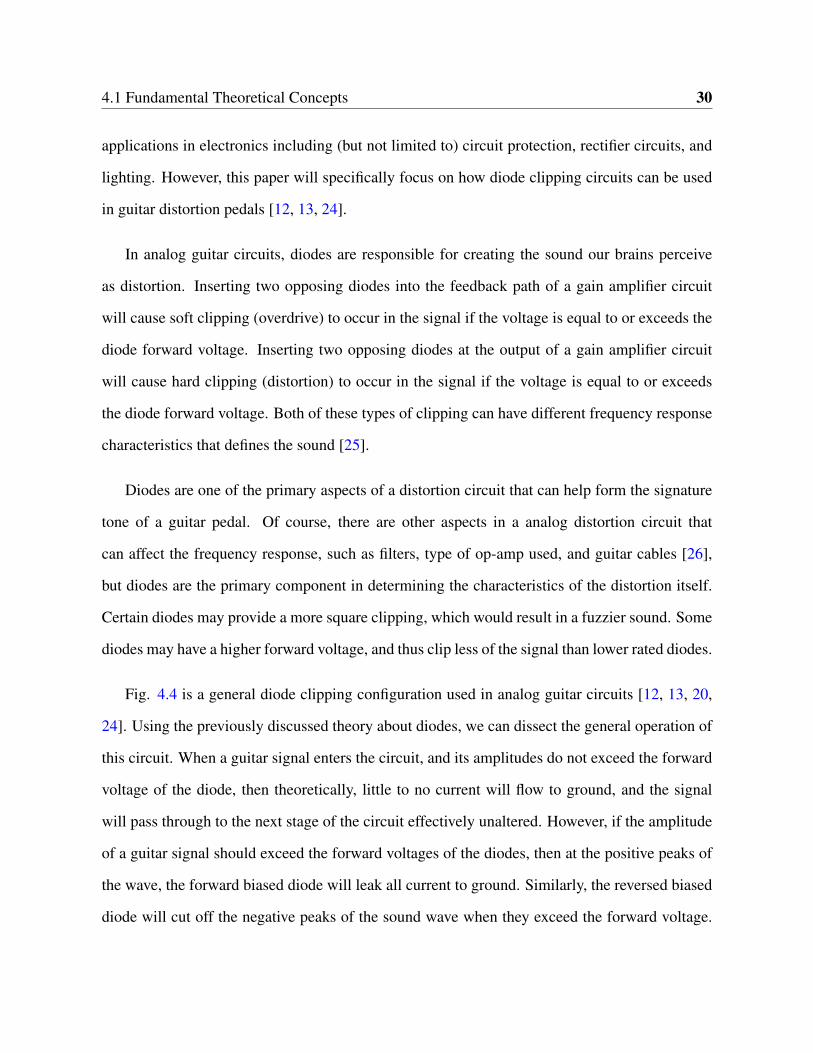
Fig. 4.4 is a general diode clipping configuration used in analog guitar circuits [12, 13, 20,
24]. Using the previously discussed theory about diodes, we can dissect the general operation of
this circuit. When a guitar signal enters the circuit, and its amplitudes do not exceed the forward
voltage of the diode, then theoretically, little to no current will flow to ground, and the signal
will pass through to the next stage of the circuit effectively unaltered. However, if the amplitude
of a guitar signal should exceed the forward voltages of the diodes, then at the positive peaks of
the wave, the forward biased diode will leak all current to ground. Similarly, the reversed biased
diode will cut off the negative peaks of the sound wave when they exceed the forward voltage.
4.2 Theoretical Design and Simulation 31
Figure 4.4: General Diode Clipping Circuit
By using gain supplied by an op-amp circuit, the user can adjust the amplitude of the waveforms
entering the clipping circuit, allowing the user to control the degree to which the diodes clip
the signal. This is the single most significant concept an engineer must understand to design an
analog distortion pedal.
4.2 Theoretical Design and Simulation
This section of the chapter aims to go over specific design decisions made in the making of the
analog distortion circuitry, and verification of chosen designs using PSPICE simulations. The
op-amp used for the theoretical PSPICE simulations was the LM741. This general purpose op-
amp is suitable for modeling purposes, but eventually will be replaced in the PCB design in favor
of a faster, lower noise amplifier.
4.2.1 Buffer Circuit Design
The buffer circuit was a necessary design decision for the circuit, as it provides isolation between
the guitar and the distortion circuitry. Many pedals in the industry use a buffer circuit at the input
and output to ensure proper transferal of a guitar signal [12, 13, 20, 24].
4.2 Theoretical Design and Simulation 32
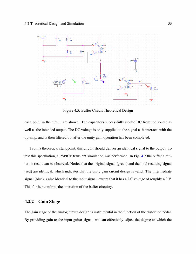
For the buffer circuit in Fig. 4.5 shows the chosen design for this application. While it is com-
mon to use emitter follower circuits when designing buffers, a unity gain op-amp configuration
was favored over the emitter follower due to its ease of design, and more modern approach.
First and foremost, the operational amplifier supply voltage was chosen to be 9 V, as it is an
industry standard for guitar pedals to have 9 V supplies, whether from wall adapter or battery.
Also, this will provide plenty of DC power for the circuit to function properly considering a
guitar signal is typically smaller in magnitude comparatively. The parallel resistors attached to
the non-inverting input of the op-amp were chosen to be 2.2MΩ. The Thevenin equivalent circuit
would result in the input impedance being approximately 1.1MΩ. These resistors help maintain
a high input resistance to the op-amp, which is an important characteristic for a buffer amplifier
circuit. Recall, guitar pickups typically have an output impedance of 5k-15kΩ [9]. By having an
input resistance of 1.1MΩ, it minimizes loading the preceding stage of the guitar pedal [24].
This circuit at the core is a unity gain op-amp. The signal enters in via the positive terminal.
The output, which is wired directly to the negative terminal, then delivers the unaltered signal
to the distortion stage of the circuit. The capacitors C1 and C2 are meant to isolate DC power
from entering or exiting the circuit. This is necessary so that a DC voltage does not enter the
guitar, or exit into the amplifier, which could cause damage to internal circuitry. Additionally, it
is important to note that capacitor C1 forms a high pass filter with the resistor R2. Due to this,
a capacitor value of 0.1 µF was chosen so that no frequencies would experience filtering at this
stage. Similarly, the output capacitor forms a low-pass filter with resistors in the following stage
of the circuit. To prevent any unwanted filtering, a large capacitor value was selected.
For this circuit, a virtual ground of 4.5 V was created using a standard voltage divider. This
virtual ground supplies 4.5 V of DC voltage to the AC guitar signal, to ensure that the voltage
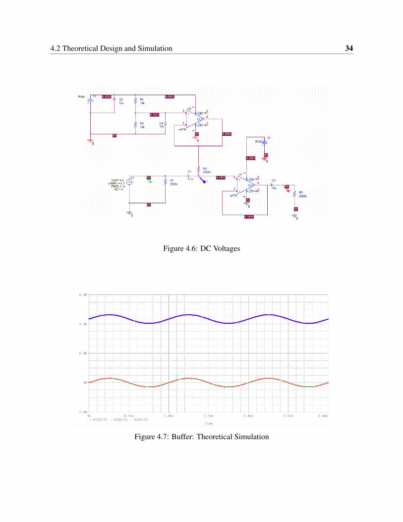
level is within suitable range of the op-amp supply voltage. In the Fig. 4.6, the DC voltages at
4.2 Theoretical Design and Simulation 33
Figure 4.5: Buffer Circuit Theoretical Design
each point in the circuit are shown. The capacitors successfully isolate DC from the source as
well as the intended output. The DC voltage is only supplied to the signal as it interacts with the
op-amp, and is then filtered out after the unity gain operation has been completed.
From a theoretical standpoint, this circuit should deliver an identical signal to the output. To
test this speculation, a PSPICE transient simulation was performed. In Fig. 4.7 the buffer simu-
lation result can be observed. Notice that the original signal (green) and the final resulting signal
(red) are identical, which indicates that the unity gain circuit design is valid. The intermediate
signal (blue) is also identical to the input signal, except that it has a DC voltage of roughly 4.3 V.
This further confirms the operation of the buffer circuitry.
4.2.2 Gain Stage
The gain stage of the analog circuit design is instrumental in the function of the distortion pedal.
By providing gain to the input guitar signal, we can effectively adjust the degree to which the
4.2 Theoretical Design and Simulation 34
Figure 4.6: DC Voltages
Figure 4.7: Buffer: Theoretical Simulation
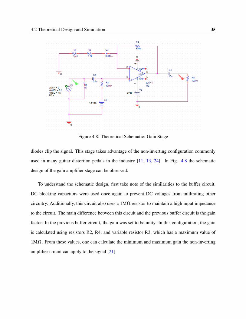
4.2 Theoretical Design and Simulation 35
Figure 4.8: Theoretical Schematic: Gain Stage
diodes clip the signal. This stage takes advantage of the non-inverting configuration commonly
used in many guitar distortion pedals in the industry [11, 13, 24]. In Fig. 4.8 the schematic
design of the gain amplifier stage can be observed.
To understand the schematic design, first take note of the similarities to the buffer circuit.
DC blocking capacitors were used once again to prevent DC voltages from infiltrating other
circuitry. Additionally, this circuit also uses a 1MΩ resistor to maintain a high input impedance
to the circuit. The main difference between this circuit and the previous buffer circuit is the gain
factor. In the previous buffer circuit, the gain was set to be unity. In this configuration, the gain
is calculated using resistors R2, R4, and variable resistor R3, which has a maximum value of
1MΩ . From these values, one can calculate the minimum and maximum gain the non-inverting
amplifier circuit can apply to the signal [21].
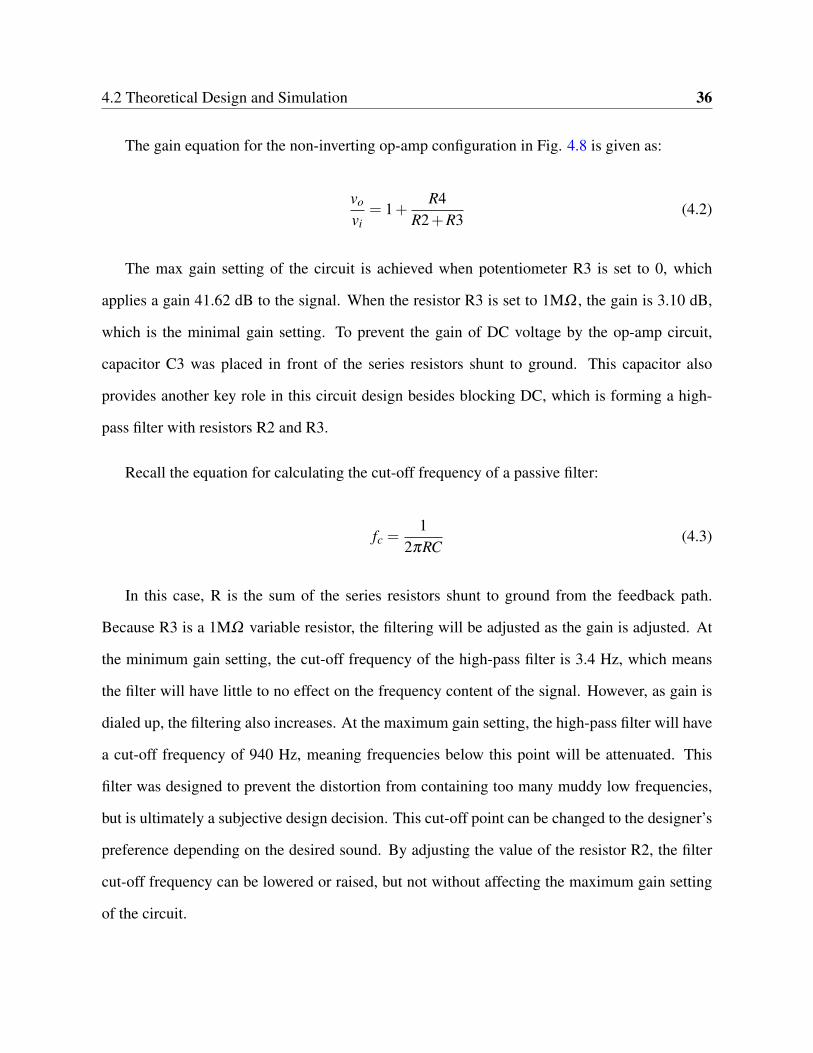
4.2 Theoretical Design and Simulation 36
The gain equation for the non-inverting op-amp configuration in Fig. 4.8 is given as:
vo
vi= 1+
R4R2+R3
(4.2)
The max gain setting of the circuit is achieved when potentiometer R3 is set to 0, which
applies a gain 41.62 dB to the signal. When the resistor R3 is set to 1MΩ , the gain is 3.10 dB,
which is the minimal gain setting. To prevent the gain of DC voltage by the op-amp circuit,
capacitor C3 was placed in front of the series resistors shunt to ground. This capacitor also
provides another key role in this circuit design besides blocking DC, which is forming a high-
pass filter with resistors R2 and R3.
Recall the equation for calculating the cut-off frequency of a passive filter:
fc =1
2πRC(4.3)
In this case, R is the sum of the series resistors shunt to ground from the feedback path.
Because R3 is a 1MΩ variable resistor, the filtering will be adjusted as the gain is adjusted. At
the minimum gain setting, the cut-off frequency of the high-pass filter is 3.4 Hz, which means
the filter will have little to no effect on the frequency content of the signal. However, as gain is
dialed up, the filtering also increases. At the maximum gain setting, the high-pass filter will have
a cut-off frequency of 940 Hz, meaning frequencies below this point will be attenuated. This
filter was designed to prevent the distortion from containing too many muddy low frequencies,
but is ultimately a subjective design decision. This cut-off point can be changed to the designer’s
preference depending on the desired sound. By adjusting the value of the resistor R2, the filter
cut-off frequency can be lowered or raised, but not without affecting the maximum gain setting
of the circuit.
4.2 Theoretical Design and Simulation 37
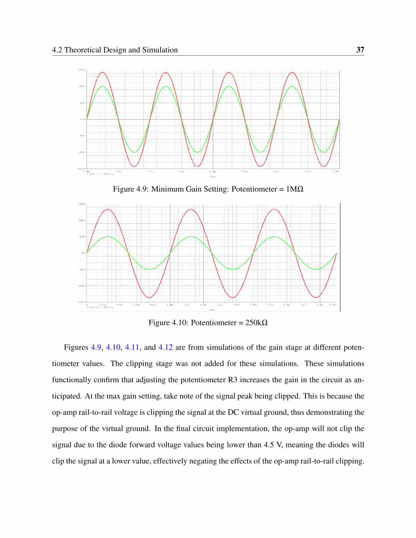
Figure 4.9: Minimum Gain Setting: Potentiometer = 1MΩ
Figure 4.10: Potentiometer = 250kΩ
Figures 4.9, 4.10, 4.11, and 4.12 are from simulations of the gain stage at different poten-
tiometer values. The clipping stage was not added for these simulations. These simulations
functionally confirm that adjusting the potentiometer R3 increases the gain in the circuit as an-
ticipated. At the max gain setting, take note of the signal peak being clipped. This is because the
op-amp rail-to-rail voltage is clipping the signal at the DC virtual ground, thus demonstrating the
purpose of the virtual ground. In the final circuit implementation, the op-amp will not clip the
signal due to the diode forward voltage values being lower than 4.5 V, meaning the diodes will
clip the signal at a lower value, effectively negating the effects of the op-amp rail-to-rail clipping.
4.2 Theoretical Design and Simulation 38
Figure 4.11: Potentiometer = 10kΩ
Figure 4.12: Maximum Gain Setting: Potentiometer = 100 Ω
4.2 Theoretical Design and Simulation 39
Figure 4.13: Gain Stage: Frequency Response
After establishing theoretical proof of concept of the gain amplifier, a frequency response
sweep was performed to gauge the frequency content of the outgoing signal. While doing a
frequency response sweep, the gain setting potentiometer was also swept to observe the effect
of changing the gain on the response of the signal. From the Fig. 4.13 it can be observed that
as the gain increases, the op-amp applies a high gain value to mid range frequencies centered at
roughly 3KHz, and attenuates frequencies between 0-900 Hz. Based on this graph, the sound of
the distortion would characteristically be rich in middle and high frequencies, and contain some
(but much less) bass frequencies. The frequency response in musical applications is generally
very subjective. Different sound profiles can appeal to different types of players. Adjusting
the frequency response for this circuit would be as simple as adjusting the passive circuitry
values in the feedback loop. Additionally, a tone control implementation would allow for further
customization of the frequency response, which will be presented in a later section of this chapter.
Selecting a different op-amp would also result in a slight change in the frequency response, but
ultimately the filters embedded within the circuit make the biggest impact on the response.
4.2 Theoretical Design and Simulation 40
Figure 4.14: Gain Stage with Hard Clipping Stage
4.2.3 Hard Clipping Stage
The hard clipping stage and the gain stage preceding it go hand-in-hand. The gain stage makes
it possible for the clipping diodes to clip the signal and create distortion. In Fig. 4.14 the gain
stage is pictured, but this time with clipping diodes at the output, and a 100k potentiometer
represented by R6. The potentiometer provides a means of volume control for the user, so that if
a louder or quieter volume is desired, simply dialing the potentiometer up or down will adjust the
amount of current leaked to ground. The hard clipping diodes used for the theoretical simulation
were silicon diodes, with a forward voltage of approximately 0.7 V. Hence, in the simulations,
we expect to see the circuit clip the output when it exceeds this voltage, rather than allow the
op-amp to clip the signal.
Before testing the capabilities of the clipping circuit, the volume potentiometer was tested
using transient simulations. In Fig. 4.15, the output signal bleeds to ground due to the low
magnitude of the potentiometer. In Figures 4.16 and 4.17, more of the signal is present at the
output due to the higher potentiometer values. This is a proof of concept, and shows that the
volume of the circuit is being properly adjusted by the variable load resistor.
4.2 Theoretical Design and Simulation 41
Figure 4.15: Volume Test: Load Resistor = 10Ω
Figure 4.16: Volume Test: Load Resistor = 1kΩ
Figure 4.17: Volume Test: Load Resistor = 100kΩ
4.2 Theoretical Design and Simulation 42
Figure 4.18: Clipping Test: Gain Resistor = 250kΩ
After confirming the functionality of the volume potentiometer, the hard clipping circuit was
tested using transient simulations. Recall, in the previous section the voltage amplitude of the
signal got up to approximately 4.3 V before being clipped by the rail-to-rail voltage of the op-
amp. In the following simulations, we should theoretically see the diode clip the signal once it
exceeds 0.7 V in amplitude. The term “clipping” refers to the flattening or rounding of the peaks
of the analog guitar signal. This effect is what musicians perceive to be distortion.
In the following three figures, the gain potentiometer was set to three different values to
demonstrate the output of the circuit at different gain levels. As shown in Fig. 4.18, the voltage
does not exceed the diode forward voltage, and therefore the signal is not clipped. In the Fig.
4.19, the circuit is set to a higher gain setting, and as a result the signal clips at roughly 0.7 V as
expected. The clipping diodes flatten out the peak of the signal, and it takes on a rounder shape
overall compared to the first simulation. In the last simulation shown in Fig. 4.20, a maximum
gain setting is shown. The peak of the signal is much more square for the final simulation because
more of the signal is being clipped by the diodes due to the increased gain. These simulations
provide justification for the hard clipping circuit design, and confirm that the theoretical design
is valid.
4.2 Theoretical Design and Simulation 43
Figure 4.19: Clipping Test: Gain Resistor = 6.2kΩ
Figure 4.20: Clipping Test: Gain Resistor = 100 Ω
4.2 Theoretical Design and Simulation 44
4.2.4 Tone Control Stage
This stage of the design is meant to offer the user a single dial tone control for a simple, yet
versatile sound. The core of this circuit is the adjustable low-pass filter circuit, which can be
seen in Fig. 4.21. Note, that the second op-amp is simply the unity gain buffer discussed in
Section 4.2.1.
The tone control stage features supporting passive circuitry at the input and output of the
circuit, whose purpose is also explained in Section 4.2.1. The main new addition this circuit
provides to the overall analog design is a means for the user to control the frequency response of
the circuit. Using resistor R4 (1.2kΩ) , and potentiometer R2 (1kΩ), a low-pass filter is formed
with capacitor C6, which was chosen to be 8.2nF . These values were chosen carefully and
intentionally using the formula for calculating the cut-off frequency of a filter [27].
Using Eqn. 4.3, when the potentiometer is set to 1k, the cut-off frequency of the low-pass
filter will be 8822 Hz. This will roll off some of the high frequencies present in the distortion
created in the clipping stage. So, if the user prefers a guitar sound with less high-end in the tone,
they can dial the potentiometer to a higher value. However, if the user desires a guitar tone with
a lot of high-frequency content, the potentiometer can be dialed to a minimum setting, which
would adjust the cut-off frequency to roughly 16.2k Hz.
This filter theoretical design was a first attempt at providing a meaningful single dial tone
control to the user. The specific values of the resistors and capacitors in the low-pass filter are
subject to some change. For example, widening the range of the cut-off frequency would be
a viable way to allow more noticeable tone control to the circuit. This would simply mean
adjusting the resistor and capacitor values, and going through the process of trial and error until
a preferable tone control frequency response is attained. For the above circuit, a frequency
4.2 Theoretical Design and Simulation 45
Figure 4.21: Tone Control Theoretical Schematic
Figure 4.22: Tone Control Frequency Response
response simulation was done to demonstrate the effect of adjusting the potentiometer. This
simulation can be seen in Fig. .
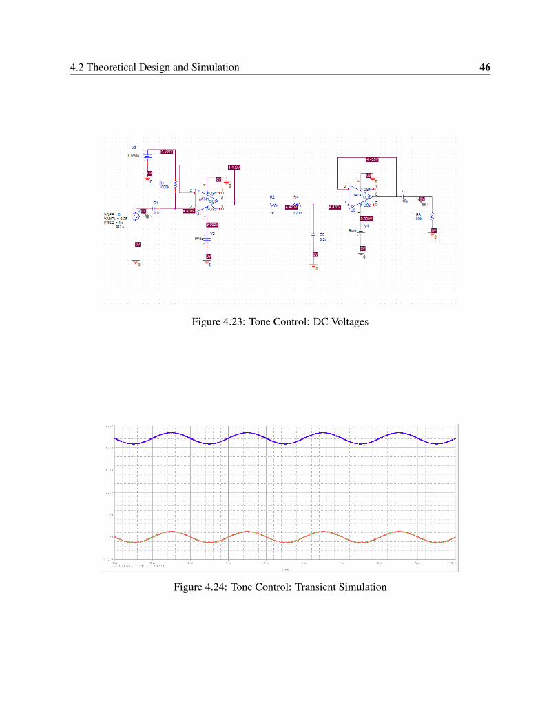
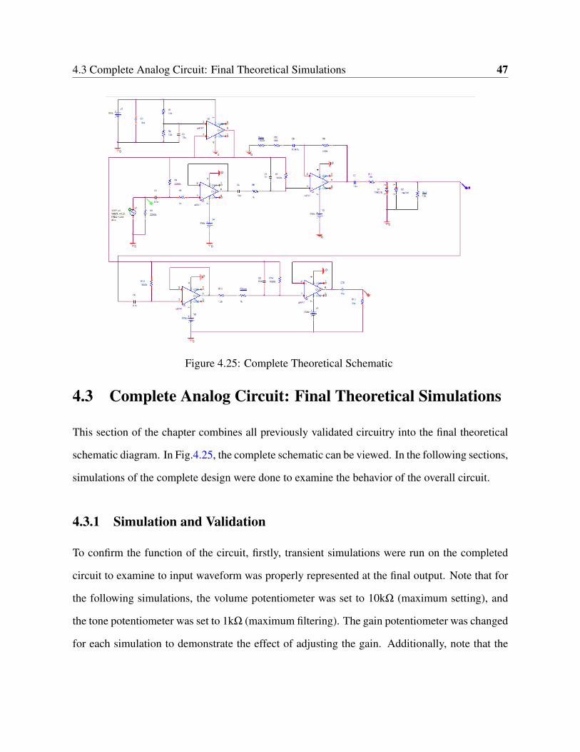
To establish proof of concept of the circuitry, the DC voltages at each point in the circuit are
shown in Fig. 4.23.. As anticipated, the blocking capacitors prevent DC from exiting the circuit
from either end of the circuit. In Fig. 4.24., a transient simulation was performed to ensure that
unity gain was maintained in this circuit. These simulations along with the frequency response
simulation conclude the demonstration of the proof of concept for the tone control circuitry.
4.2 Theoretical Design and Simulation 46
Figure 4.23: Tone Control: DC Voltages
Figure 4.24: Tone Control: Transient Simulation
4.3 Complete Analog Circuit: Final Theoretical Simulations 47
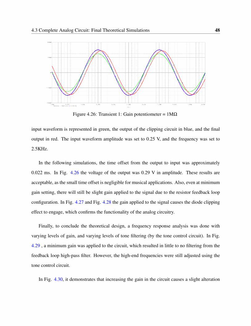
Figure 4.25: Complete Theoretical Schematic
4.3 Complete Analog Circuit: Final Theoretical Simulations
This section of the chapter combines all previously validated circuitry into the final theoretical
schematic diagram. In Fig.4.25, the complete schematic can be viewed. In the following sections,
simulations of the complete design were done to examine the behavior of the overall circuit.
4.3.1 Simulation and Validation
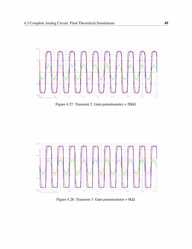
To confirm the function of the circuit, firstly, transient simulations were run on the completed
circuit to examine to input waveform was properly represented at the final output. Note that for
the following simulations, the volume potentiometer was set to 10kΩ (maximum setting), and
the tone potentiometer was set to 1kΩ (maximum filtering). The gain potentiometer was changed
for each simulation to demonstrate the effect of adjusting the gain. Additionally, note that the
4.3 Complete Analog Circuit: Final Theoretical Simulations 48
Figure 4.26: Transient 1: Gain potentiometer = 1MΩ
input waveform is represented in green, the output of the clipping circuit in blue, and the final
output in red. The input waveform amplitude was set to 0.25 V, and the frequency was set to
2.5KHz.
In the following simulations, the time offset from the output to input was approximately
0.022 ms. In Fig. 4.26 the voltage of the output was 0.29 V in amplitude. These results are
acceptable, as the small time offset is negligible for musical applications. Also, even at minimum
gain setting, there will still be slight gain applied to the signal due to the resistor feedback loop
configuration. In Fig. 4.27 and Fig. 4.28 the gain applied to the signal causes the diode clipping
effect to engage, which confirms the functionality of the analog circuitry.
Finally, to conclude the theoretical design, a frequency response analysis was done with
varying levels of gain, and varying levels of tone filtering (by the tone control circuit). In Fig.
4.29 , a minimum gain was applied to the circuit, which resulted in little to no filtering from the
feedback loop high-pass filter. However, the high-end frequencies were still adjusted using the
tone control circuit.
In Fig. 4.30, it demonstrates that increasing the gain in the circuit causes a slight alteration
4.3 Complete Analog Circuit: Final Theoretical Simulations 49
Figure 4.27: Transient 2: Gain potentiometer = 20kΩ
Figure 4.28: Transient 3: Gain potentiometer = 8kΩ
4.3 Complete Analog Circuit: Final Theoretical Simulations 50
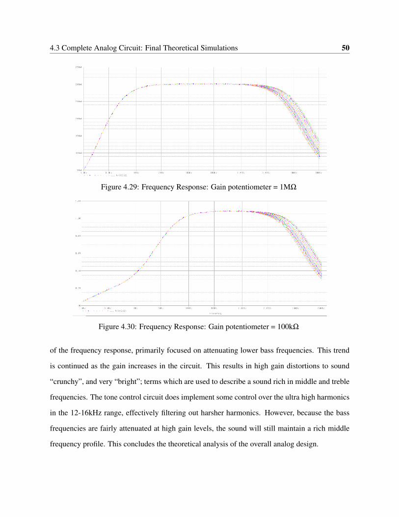
Figure 4.29: Frequency Response: Gain potentiometer = 1MΩ
Figure 4.30: Frequency Response: Gain potentiometer = 100kΩ
of the frequency response, primarily focused on attenuating lower bass frequencies. This trend
is continued as the gain increases in the circuit. This results in high gain distortions to sound
“crunchy”, and very “bright”; terms which are used to describe a sound rich in middle and treble
frequencies. The tone control circuit does implement some control over the ultra high harmonics
in the 12-16kHz range, effectively filtering out harsher harmonics. However, because the bass
frequencies are fairly attenuated at high gain levels, the sound will still maintain a rich middle
frequency profile. This concludes the theoretical analysis of the overall analog design.
4.3 Complete Analog Circuit: Final Theoretical Simulations 51
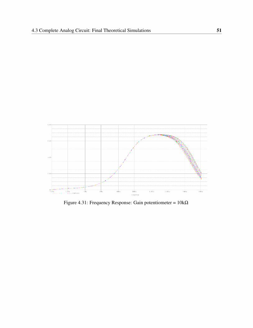
Figure 4.31: Frequency Response: Gain potentiometer = 10kΩ
Chapter 5
Hardware Analysis and Testing
In this chapter of the paper, the aim is to go over in detail the physical application of the designed
analog distortion pedal. Using the schematic presented in the previous chapter, a bread-board
version of the circuit was constructed and tested to validate the function of the design. In the
following sections, observations about the sound, and results will be discussed in further detail.
5.1 Final Hardware Schematic and PCB Layout
In Fig. 5.1 the final schematic design was constructed. There are a few notable differences in this
schematic design compared to the theoretical schematic, but the overall architecture remains the
same. Most of these adjustments consist of slight changes in passive circuitry values, primarily
for the gain stage and the tone stage. While these changes are subtle at first glance, the impact
on the frequency response is significant.
The first key difference between this schematic and the theoretical schematic is the series DC-
blocking capacitor connected to the feedback loop of the gain stage. In the theoretical schematic,
this value was chosen to be 0.047 microfarads. In the Altium schematic, this value was adjusted
5.1 Final Hardware Schematic and PCB Layout 53
to 0.062 micro-farads. The reason for this adjustment was to adjust the frequency filtering at
high gain values. In the theoretical schematic, at the highest gain setting, the high-pass cut-off
frequency was 940 Hz. By doing this, bass frequencies were highly attenuated at high gain
settings, leaving the frequency response to contain mostly middle and high frequencies. This
created a very bright, thin tone as a result. This isn’t necessarily a good or bad characteristic;
some guitarists may prefer this type of tone. Regardless, by replacing this capacitor with a
0.062 micro-farad capacitor, the high-pass cut-off frequency (at maximum gain) was adjusted to
713 Hz. This allowed for less filtering of bass frequencies, giving the sound a fuller feel while
also maintaining a clear tone. Some experimentation was done with lower cut-off frequencies
between 500-650 Hz, but the sound was found to be too muddy in quality. Designing a cut-off
frequency of 713 Hz seemed to be a reasonable middle ground, with the best tonal quality.
Another slight adjustment made was to the theoretical tone control. Recall, that the low-pass
cut-off frequency range was set to 8.8-15.9 kHz. As discussed previously, this filter was meant to
give a subtle high-end adjustment to the frequency range of the circuit. By replacing the previous
low-pass filter components with a 1 kΩ series resistor, and a 10 nF capacitor, the frequency range
of the tone dial was fixed to 7.9 kHz-15.9 kHz. This change does not majorly affect the sound, but
does prove that the circuit can be later modified to further adjust the tone control. It is reasonable
to expect that this circuit could be modified in a future iteration to improve the effectiveness of
the tone control.
One final key adjustment was the addition of an analog 3PDT switch. This switch essentially
allows the user to bypass the effect completely when switch off, and enable the distortion effect
when switched off. By stomping on the metal analog switch, the user can instantaneously add
distortion to an otherwise clean signal. This can be extremely useful for songs which require both
clean and dirty guitar sections. A small series resistor LED circuit was added to the switch as
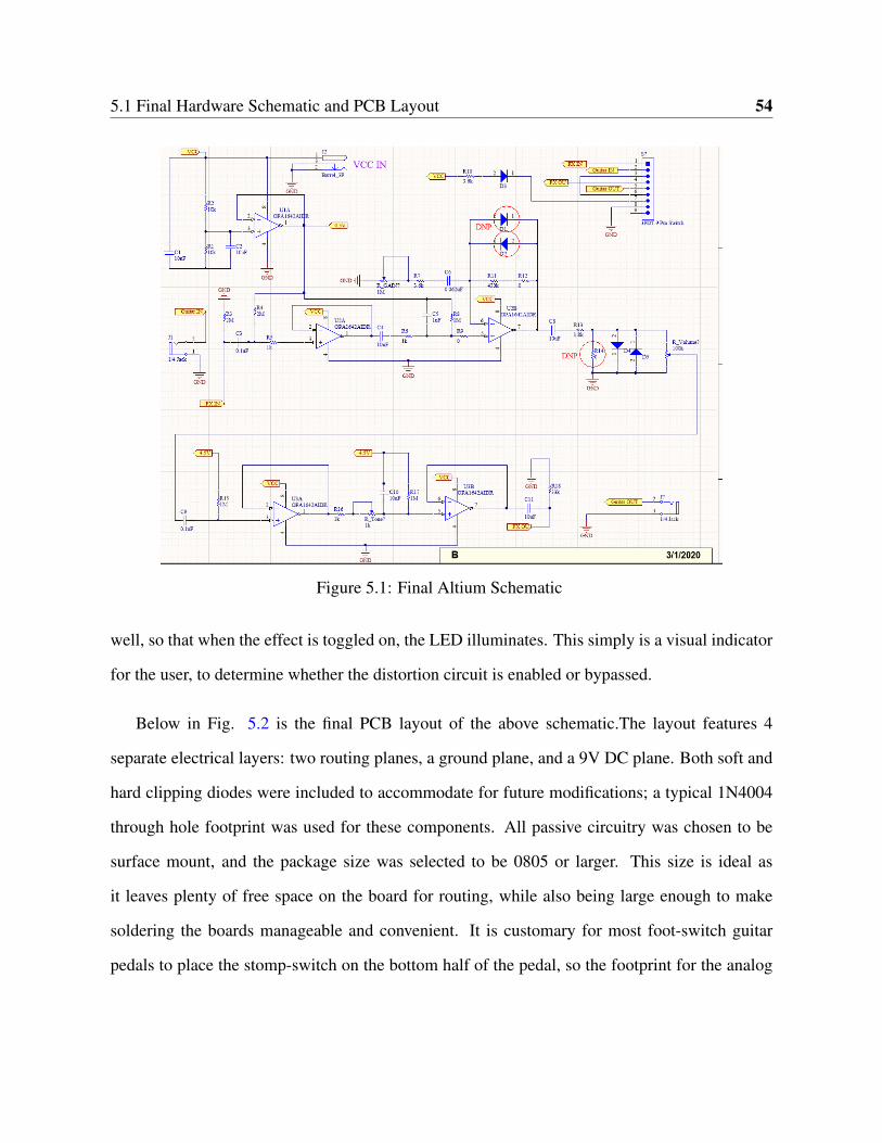
5.1 Final Hardware Schematic and PCB Layout 54
Figure 5.1: Final Altium Schematic
well, so that when the effect is toggled on, the LED illuminates. This simply is a visual indicator
for the user, to determine whether the distortion circuit is enabled or bypassed.
Below in Fig. 5.2 is the final PCB layout of the above schematic.The layout features 4
separate electrical layers: two routing planes, a ground plane, and a 9V DC plane. Both soft and
hard clipping diodes were included to accommodate for future modifications; a typical 1N4004
through hole footprint was used for these components. All passive circuitry was chosen to be
surface mount, and the package size was selected to be 0805 or larger. This size is ideal as
it leaves plenty of free space on the board for routing, while also being large enough to make
soldering the boards manageable and convenient. It is customary for most foot-switch guitar
pedals to place the stomp-switch on the bottom half of the pedal, so the footprint for the analog
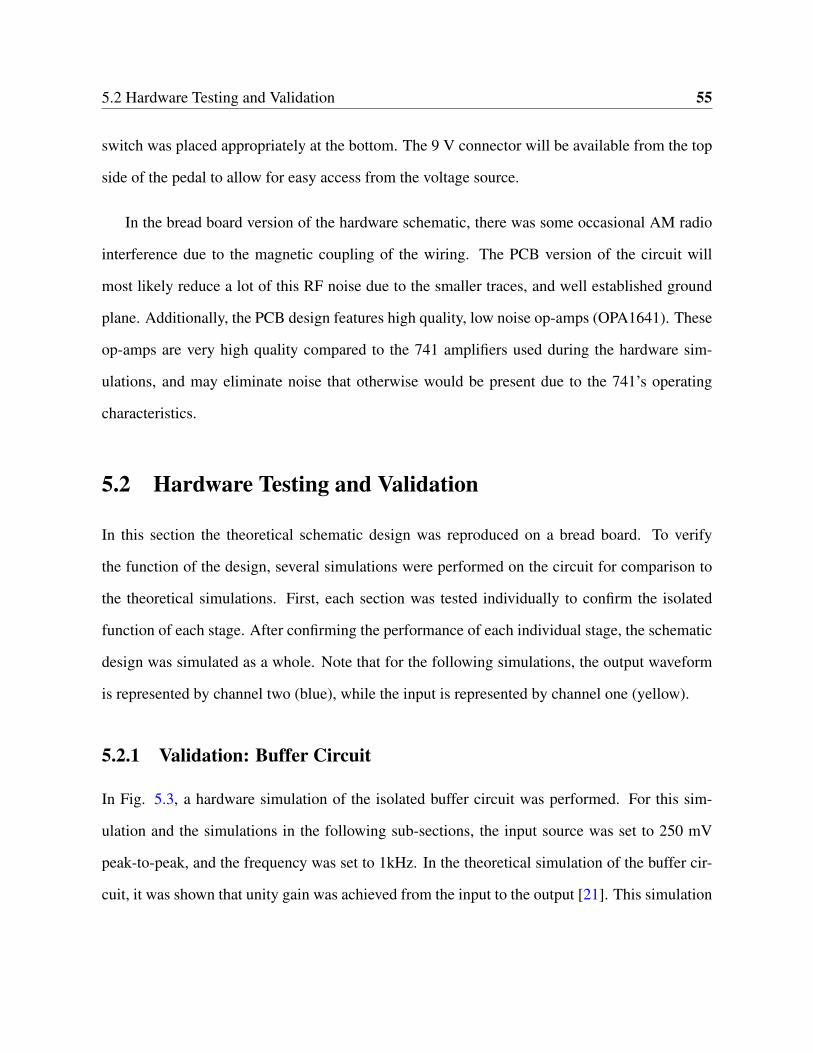
5.2 Hardware Testing and Validation 55
switch was placed appropriately at the bottom. The 9 V connector will be available from the top
side of the pedal to allow for easy access from the voltage source.
In the bread board version of the hardware schematic, there was some occasional AM radio
interference due to the magnetic coupling of the wiring. The PCB version of the circuit will
most likely reduce a lot of this RF noise due to the smaller traces, and well established ground
plane. Additionally, the PCB design features high quality, low noise op-amps (OPA1641). These
op-amps are very high quality compared to the 741 amplifiers used during the hardware sim-
ulations, and may eliminate noise that otherwise would be present due to the 741’s operating
characteristics.
5.2 Hardware Testing and Validation
In this section the theoretical schematic design was reproduced on a bread board. To verify
the function of the design, several simulations were performed on the circuit for comparison to
the theoretical simulations. First, each section was tested individually to confirm the isolated
function of each stage. After confirming the performance of each individual stage, the schematic
design was simulated as a whole. Note that for the following simulations, the output waveform
is represented by channel two (blue), while the input is represented by channel one (yellow).
5.2.1 Validation: Buffer Circuit
In Fig. 5.3, a hardware simulation of the isolated buffer circuit was performed. For this sim-
ulation and the simulations in the following sub-sections, the input source was set to 250 mV
peak-to-peak, and the frequency was set to 1kHz. In the theoretical simulation of the buffer cir-
cuit, it was shown that unity gain was achieved from the input to the output [21]. This simulation
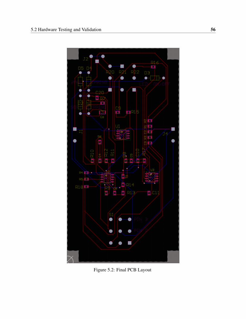
5.2 Hardware Testing and Validation 56
Figure 5.2: Final PCB Layout
5.2 Hardware Testing and Validation 57
Figure 5.3: Hardware Buffer Simulation
confirms the function of the buffer circuit. Due to noise in the circuit, the output hovers around
270 mV rather than 250 mV (peak-to-peak). However, this difference is negligible in the func-
tion of the overall circuit. Therefore, it can be concluded that the buffer circuit hardware design
matches the intended function demonstrated in the theoretical section.
5.2.2 Validation: Gain Stage with Hard Clipping
Next, the validation of the gain stage with hard clipping was done using several simulations with
varying gain potentiometer values. Recall, a 1MΩ potentiometer connected to the feedback path
of the op. amp is responsible for dialing in the gain for the circuit. The lowest possible gain
setting in this case being when the potentiometer is set to 1MΩ.
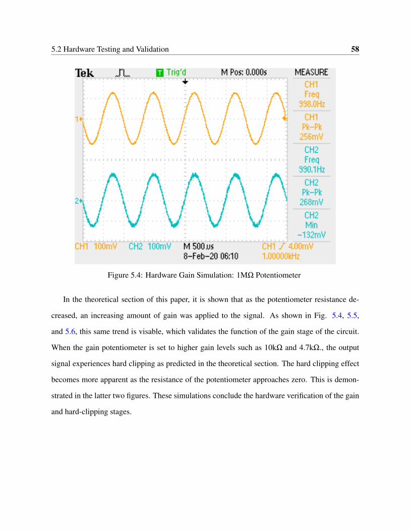
5.2 Hardware Testing and Validation 58
Figure 5.4: Hardware Gain Simulation: 1MΩ Potentiometer
In the theoretical section of this paper, it is shown that as the potentiometer resistance de-
creased, an increasing amount of gain was applied to the signal. As shown in Fig. 5.4, 5.5,
and 5.6, this same trend is visable, which validates the function of the gain stage of the circuit.
When the gain potentiometer is set to higher gain levels such as 10kΩ and 4.7kΩ., the output
signal experiences hard clipping as predicted in the theoretical section. The hard clipping effect
becomes more apparent as the resistance of the potentiometer approaches zero. This is demon-
strated in the latter two figures. These simulations conclude the hardware verification of the gain
and hard-clipping stages.
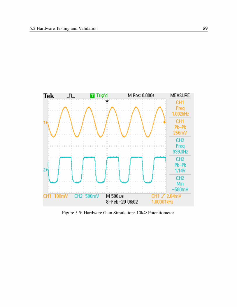
5.2 Hardware Testing and Validation 59
Figure 5.5: Hardware Gain Simulation: 10kΩ Potentiometer
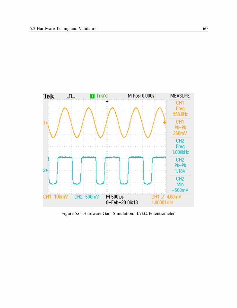
5.2 Hardware Testing and Validation 60
Figure 5.6: Hardware Gain Simulation: 4.7kΩ Potentiometer
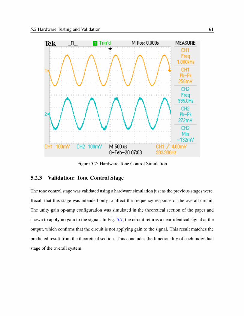
5.2 Hardware Testing and Validation 61
Figure 5.7: Hardware Tone Control Simulation
5.2.3 Validation: Tone Control Stage
The tone control stage was validated using a hardware simulation just as the previous stages were.
Recall that this stage was intended only to affect the frequency response of the overall circuit.
The unity gain op-amp configuration was simulated in the theoretical section of the paper and
shown to apply no gain to the signal. In Fig. 5.7, the circuit returns a near-identical signal at the
output, which confirms that the circuit is not applying gain to the signal. This result matches the
predicted result from the theoretical section. This concludes the functionality of each individual
stage of the overall system.
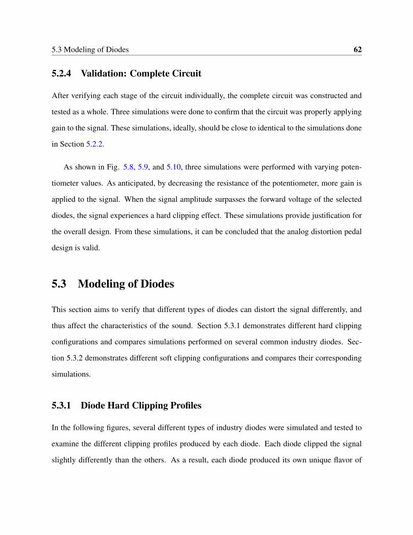
5.3 Modeling of Diodes 62
5.2.4 Validation: Complete Circuit
After verifying each stage of the circuit individually, the complete circuit was constructed and
tested as a whole. Three simulations were done to confirm that the circuit was properly applying
gain to the signal. These simulations, ideally, should be close to identical to the simulations done
in Section 5.2.2.
As shown in Fig. 5.8, 5.9, and 5.10, three simulations were performed with varying poten-
tiometer values. As anticipated, by decreasing the resistance of the potentiometer, more gain is
applied to the signal. When the signal amplitude surpasses the forward voltage of the selected
diodes, the signal experiences a hard clipping effect. These simulations provide justification for
the overall design. From these simulations, it can be concluded that the analog distortion pedal
design is valid.
5.3 Modeling of Diodes
This section aims to verify that different types of diodes can distort the signal differently, and
thus affect the characteristics of the sound. Section 5.3.1 demonstrates different hard clipping
configurations and compares simulations performed on several common industry diodes. Sec-
tion 5.3.2 demonstrates different soft clipping configurations and compares their corresponding
simulations.
5.3.1 Diode Hard Clipping Profiles
In the following figures, several different types of industry diodes were simulated and tested to
examine the different clipping profiles produced by each diode. Each diode clipped the signal
slightly differently than the others. As a result, each diode produced its own unique flavor of

5.3 Modeling of Diodes 63
Figure 5.8: Hardware Gain Simulation: 1MΩ Potentiometer
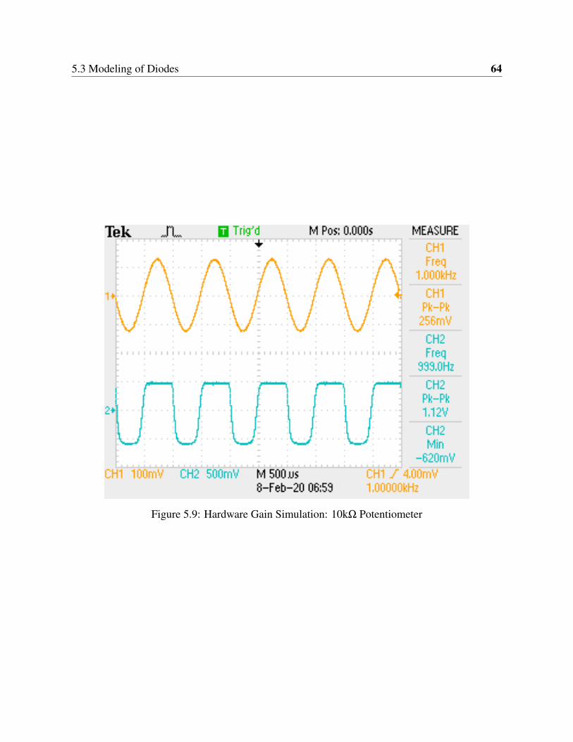
5.3 Modeling of Diodes 64
Figure 5.9: Hardware Gain Simulation: 10kΩ Potentiometer
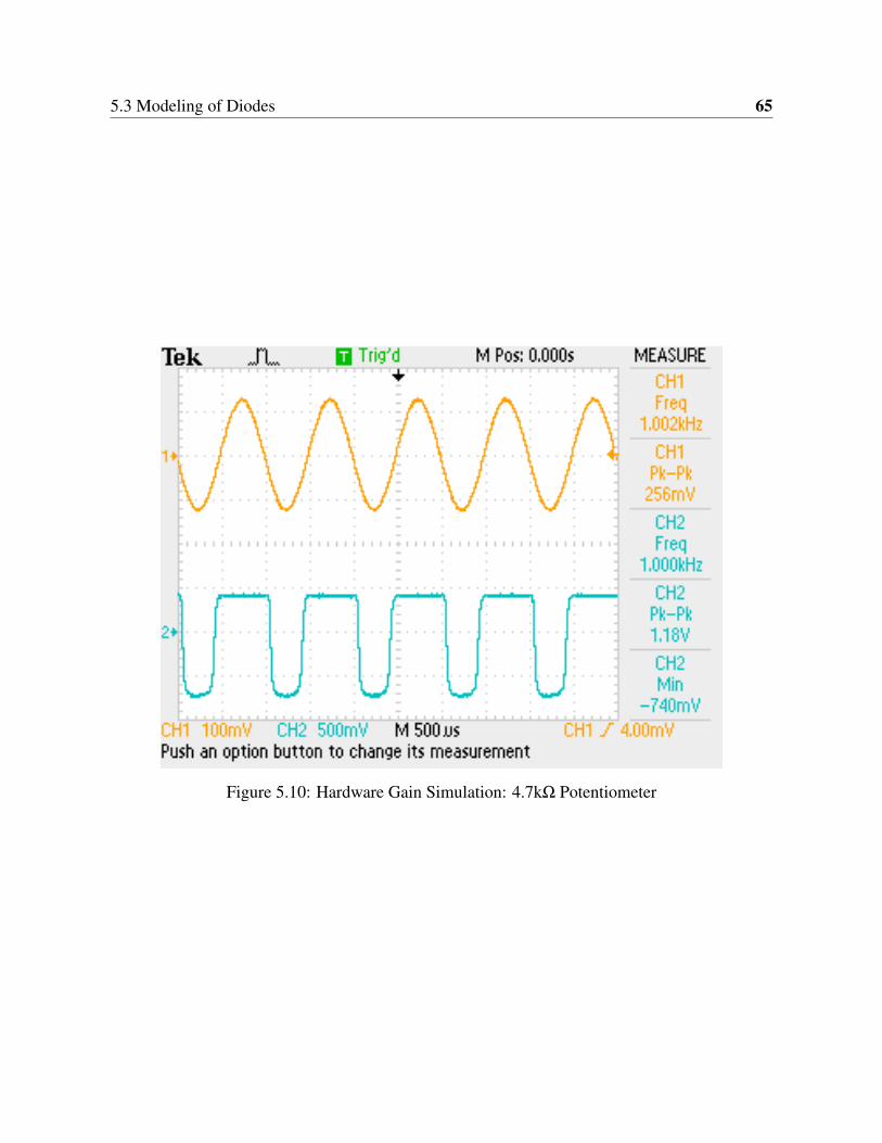
5.3 Modeling of Diodes 65
Figure 5.10: Hardware Gain Simulation: 4.7kΩ Potentiometer
5.3 Modeling of Diodes 66
distortion [12]. The differences between the diodes were subtle overall, but noticeable to any
regularly practicing musician.
To minimize sources of error, each diode was tested using the same Gibson Les Paul, with
the exact same amplifier settings. Doing this ensures that the tonal differences between each
diode are accented. Additionally, the same guitar cable was also used to ensure that the inherent
characteristics of the cable would not contribute to the tone differences for each trial [9] . In
the following simulations, the pedal volume was kept at the maximum, and the gain was set to
a high setting (20k) to properly demonstrate the clipping effect. A 1kHz signal with a 100 mV
amplitude was used to simulate a guitar signal in each of the simulations below.
The first simulation in Fig. 5.11, was of the 1N4735. This is a common industry silicon zener
diode with a nominal forward voltage of roughly 1.2 V (at the maximum current setting). The
higher forward voltage of this diode caused the signal to clip in a less harsh manner compared to
the other diodes with lower forward voltages, which resulted in a less fuzzy type of distortion.
Generally speaking, the sound wasn’t overly fuzzy, but didn’t lack in fuzz either. A wide range
of frequencies seemed to be present in the signal, and it seemed fairly balanced. Notice that
the measured peak-to-peak voltage of the signal is roughly 1.34 V. This is higher than all of the
other diodes tested in this section, which indicates that less of the signal is being hard clipped.
Overall, the sound seemed to be fairly representative of a typical hard clipping sound profile that
guitarists look for in classic rock.
The second simulation in Fig. 5.12, was of the 1N4148. This is another common silicon
diode with a nominal forward voltage of 0.7-1 V (depending on the amount of current through
the diode). This diode seemed to clip the signal at a lower level compared to the 1N4735, as
indicated by the peak-to-peak voltage measurement of 1.11 V. Still, the sound profile seemed to
represent a classic rock profile in a similar manner to the 1N4735. There were a lot of middle
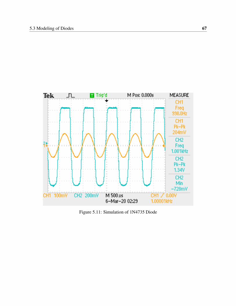
5.3 Modeling of Diodes 67
Figure 5.11: Simulation of 1N4735 Diode
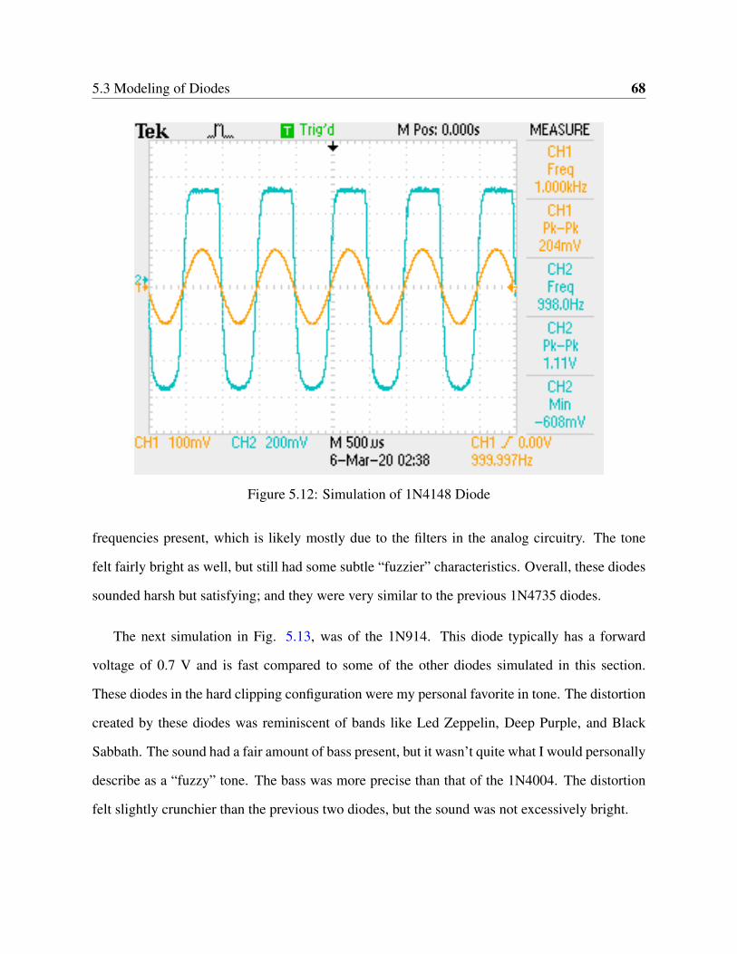
5.3 Modeling of Diodes 68
Figure 5.12: Simulation of 1N4148 Diode
frequencies present, which is likely mostly due to the filters in the analog circuitry. The tone
felt fairly bright as well, but still had some subtle “fuzzier” characteristics. Overall, these diodes
sounded harsh but satisfying; and they were very similar to the previous 1N4735 diodes.
The next simulation in Fig. 5.13, was of the 1N914. This diode typically has a forward
voltage of 0.7 V and is fast compared to some of the other diodes simulated in this section.
These diodes in the hard clipping configuration were my personal favorite in tone. The distortion
created by these diodes was reminiscent of bands like Led Zeppelin, Deep Purple, and Black
Sabbath. The sound had a fair amount of bass present, but it wasn’t quite what I would personally
describe as a “fuzzy” tone. The bass was more precise than that of the 1N4004. The distortion
felt slightly crunchier than the previous two diodes, but the sound was not excessively bright.
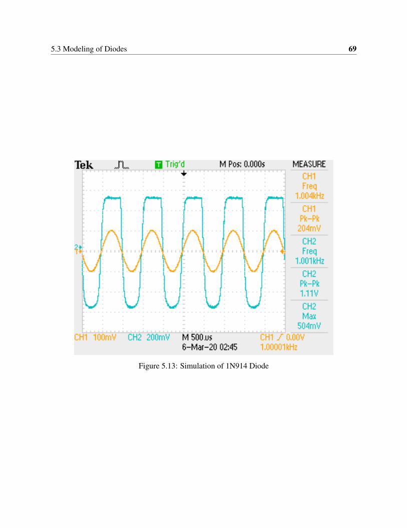
5.3 Modeling of Diodes 69
Figure 5.13: Simulation of 1N914 Diode
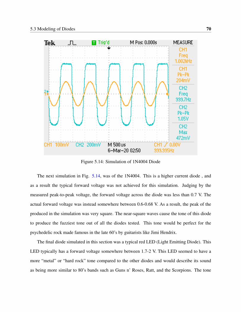
5.3 Modeling of Diodes 70
Figure 5.14: Simulation of 1N4004 Diode
The next simulation in Fig. 5.14, was of the 1N4004. This is a higher current diode , and
as a result the typical forward voltage was not achieved for this simulation. Judging by the
measured peak-to-peak voltage, the forward voltage across the diode was less than 0.7 V. The
actual forward voltage was instead somewhere between 0.6-0.68 V. As a result, the peak of the
produced in the simulation was very square. The near-square waves cause the tone of this diode
to produce the fuzziest tone out of all the diodes tested. This tone would be perfect for the
psychedelic rock made famous in the late 60’s by guitarists like Jimi Hendrix.
The final diode simulated in this section was a typical red LED (Light Emitting Diode). This
LED typically has a forward voltage somewhere between 1.7-2 V. This LED seemed to have a
more “metal” or “hard rock” tone compared to the other diodes and would describe its sound
as being more similar to 80’s bands such as Guns n’ Roses, Ratt, and the Scorpions. The tone
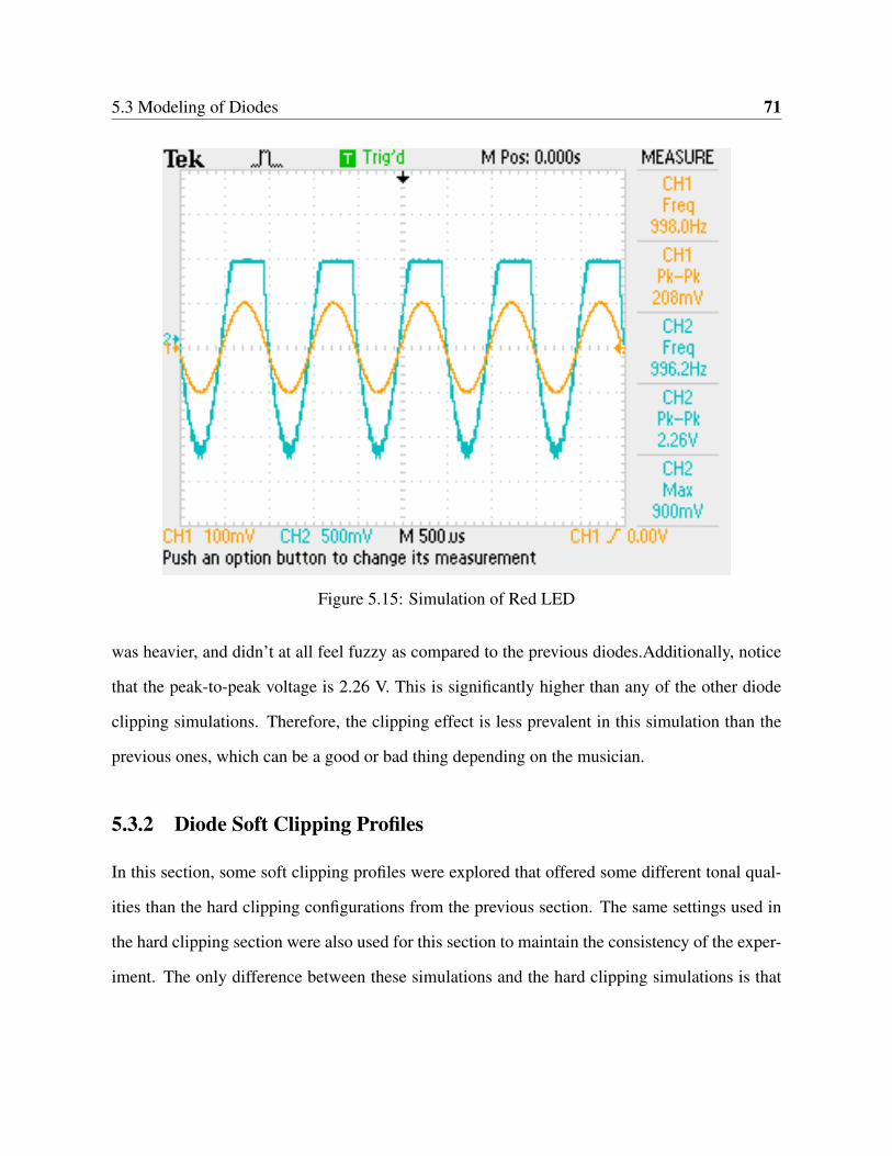
5.3 Modeling of Diodes 71
Figure 5.15: Simulation of Red LED
was heavier, and didn’t at all feel fuzzy as compared to the previous diodes.Additionally, notice
that the peak-to-peak voltage is 2.26 V. This is significantly higher than any of the other diode
clipping simulations. Therefore, the clipping effect is less prevalent in this simulation than the
previous ones, which can be a good or bad thing depending on the musician.
5.3.2 Diode Soft Clipping Profiles
In this section, some soft clipping profiles were explored that offered some different tonal qual-
ities than the hard clipping configurations from the previous section. The same settings used in
the hard clipping section were also used for this section to maintain the consistency of the exper-
iment. The only difference between these simulations and the hard clipping simulations is that
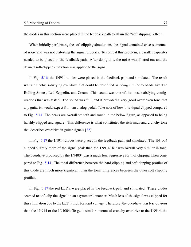
5.3 Modeling of Diodes 72
the diodes in this section were placed in the feedback path to attain the “soft slipping” effect.
When initially performing the soft clipping simulations, the signal contained excess amounts
of noise and was not distorting the signal properly. To combat this problem, a parallel capacitor
needed to be placed in the feedback path. After doing this, the noise was filtered out and the
desired soft-clipped distortion was applied to the signal.
In Fig. 5.16, the 1N914 diodes were placed in the feedback path and simulated. The result
was a crunchy, satisfying overdrive that could be described as being similar to bands like The
Rolling Stones, Led Zeppelin, and Cream. This sound was one of the most satisfying config-
urations that was tested. The sound was full, and it provided a very good overdriven tone that
any guitarist would expect from an analog pedal. Take note of how this signal clipped compared
to Fig. 5.13. The peaks are overall smooth and round in the below figure, as opposed to being
harshly clipped and square. This difference is what constitutes the rich mids and crunchy tone
that describes overdrive in guitar signals [22].
In Fig. 5.17 the 1N914 diodes were placed in the feedback path and simulated. The 1N4004
clipped slightly more of the signal peak than the 1N914, but was overall very similar in tone.
The overdrive produced by the 1N4004 was a much less aggressive form of clipping when com-
pared to Fig. 5.14. The tonal difference between the hard clipping and soft clipping profiles of
this diode are much more significant than the tonal differences between the other soft clipping
profiles.
In Fig. 5.17 the red LED’s were placed in the feedback path and simulated. These diodes
seemed to soft clip the signal in an asymmetric manner. Much less of the signal was clipped for
this simulation due to the LED’s high forward voltage. Therefore, the overdrive was less obvious
than the 1N914 or the 1N4004. To get a similar amount of crunchy overdrive to the 1N914, the
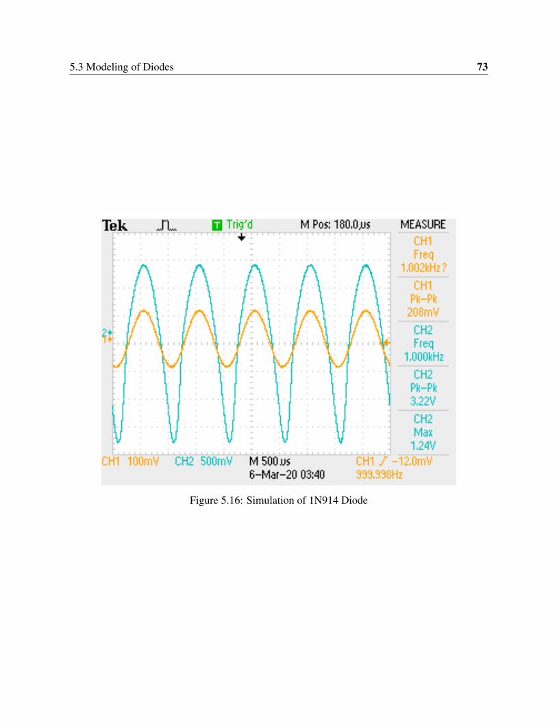
5.3 Modeling of Diodes 73
Figure 5.16: Simulation of 1N914 Diode
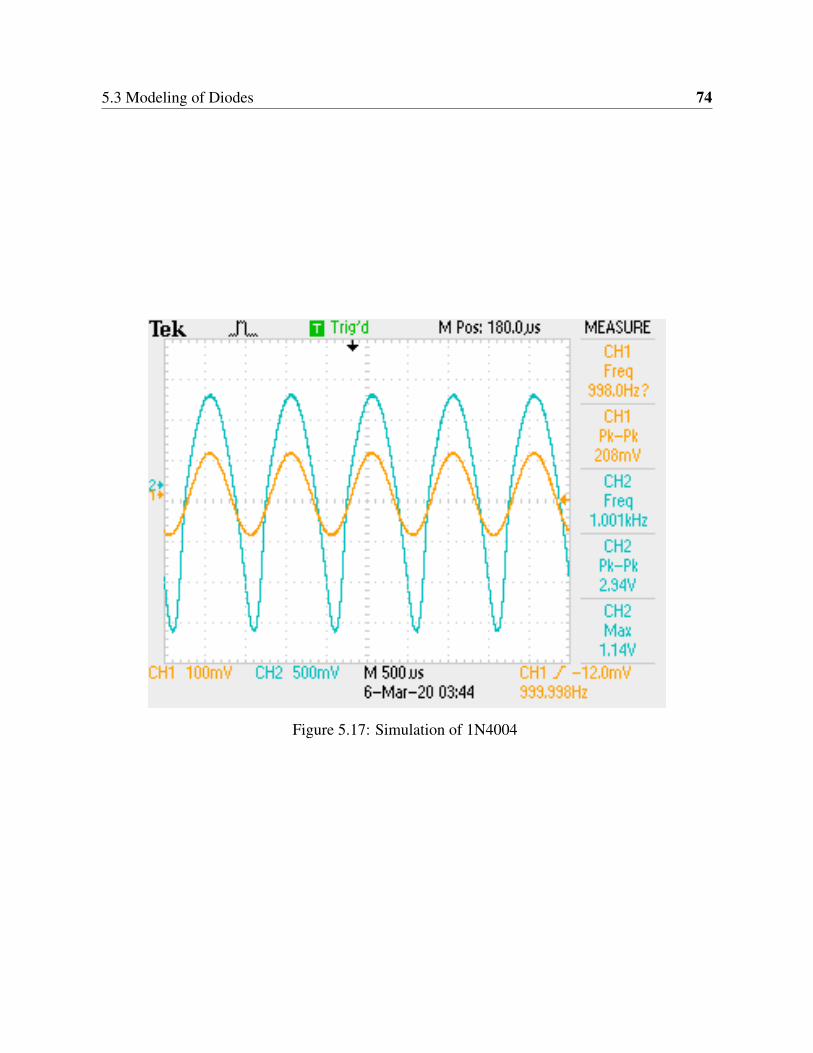
5.3 Modeling of Diodes 74
Figure 5.17: Simulation of 1N4004
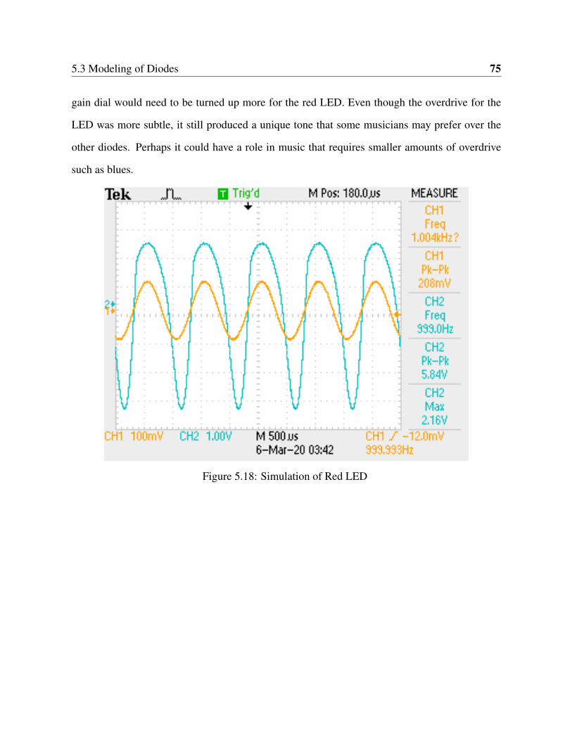
5.3 Modeling of Diodes 75
gain dial would need to be turned up more for the red LED. Even though the overdrive for the
LED was more subtle, it still produced a unique tone that some musicians may prefer over the
other diodes. Perhaps it could have a role in music that requires smaller amounts of overdrive
such as blues.
Figure 5.18: Simulation of Red LED
Chapter 6
Conclusions
This chapter summarizes this research project and presents possible future work associated with
the project.
6.1 Summary of Results
The analog distortion circuitry designed in this project functioned as expected, and the distortion
created by the circuit was both distinct and satisfying. The final pedal design was simple, yet
versatile. The gain dial offered many different levels of distortion which any future user can
change as needed. The tone dial provided some filtering for some of the higher frequencies
produced during distortion. Lastly, the volume dial ensured that the user could adjust the amount
of the signal being output to accommodate for different auditory levels. The diodes tested in the
hardware chapter provided some examples of how different diodes can clip the signal differently.
Some musicians may be striving for a fuzzier, more square distortion, which the 1N4004 was
well suited for. Other musicians may prefer the classic crunchy tones of the Rolling Stones and
Deep Purple, which the 1N914 represented well. Overall, the pedal exceeded expectations. The
6.2 Outlook and Future Work 77
audio quality of the distortion was up to par with other standard analog pedals on the market.
6.2 Outlook and Future Work
While the project was successful in producing its promised deliverables, there are some mod-
ifications that could further improve the versatility of the pedal. In a future project, it would
be beneficial to add a three band equalization, which would allow for further customization of
the frequency response. Additionally, the PCB was intentionally left with unpopulated diode
terminals. The user can modify the pedal manually by swapping out the clipping diodes.
Outside of this specific project, some other related future work could include designing other
types of guitar pedal effects such as chorus, delay, and reverb. Many of these effects also rely on
analog circuitry to alter the signal from a guitar. Using the knowledge basis that this project has
provided, many other guitar-related engineering projects could be explored further.
References
[1] Guadagnin, Leo and Lihoreau, Bertrand and Lotton, Perrick and Brasseur, Emmanual.
Analytical Modeling and Experimental Characterization of a Magnetic Pickup for Elec-
tric Guitar. Journal of the Audio Engineering Society, 65(9):711–721, sep 2017. doi:
10.17743/jaes.2017.0024.
[2] Horton, Nicholas G. and Moore, Thomas R. Modeling the Magnetic Pickup of an Electric
Guitar. American Journal of Physics, 77(2):144–150, feb 2009. doi:10.1119/1.2990663.
[3] Bussey, W. Stephen and Haigler, Robert M. Tubes versus transistors in electric guitar am-
plifiers. In ICASSP ’81. IEEE International Conference on Acoustics, Speech, and Signal
Processing. IEEE, March 1981. doi:10.1109/ICASSP.1981.1171205.
[4] Covert, John and Livingston, David. A Vacuum Tube Guitar Amplifier Model Using a
Recurrent Neural Network. In 2013 Proceedings of IEEE Southeastcon. IEEE, 2013. doi:
10.1109/SECON.2013.6567472.
[5] Yeh, David and Abel, Jonathan and Smith, Julius and Vladimirescu, Andrei. Numerical
Methods for Simulation of Guitar Distortion Circuits. In IEEE Transaction, 2008. doi:
10.1162/comj.2008.32.2.23.
[6] Kenneth Smith. Microelectronic Circuits Seventh Edition. Oxford University Press, 2014.
References 79
[7] Lemarquand, G. and Lemarquand, V. Calculation Method of Permanent-Magnet Pickups
for Electric Guitars. IEEE Transactions on Magnetics, 43(9):3573–3578, sep 2007. doi:
10.1109/tmag.2007.891671.
[8] Jyri, Pakarinen. Modeling of Nonlinear and Time Varying Phenomena In The Guitar. In
Helsinki University of Technology Access, 2008.
[9] Paiva, Rafael C. D. and Pakarinen, Jyri and Valimaki, Vesa. Acoustics and Modeling and
of Pickups. In Journal of the AES Volume 60, 2012. URL: http://www.aes.org/e-lib/
browse.cfm?elib=16551.
[10] Barbour, Eric. The Cool Sound of Tubes. IEEE Spectrum, August 1998. doi:10.1109/
6.708439.
[11] Murthy, Anarghya Ananda and Rao, Nitish and Beemaiah, Yatheesha Ranganahalli and
Shandilya, Sushanth D. and Siddegowda, Ranjith Badarmanahalli. Design and Construction
of Arduino-Hacked Variable Gating Distortion Pedal. IEEE Access, 2:1409–1417, 2014.
doi:10.1109/access.2014.2374195.
[12] Huang, Kai-Chieh. King of Tone Guitar Pedal Modeling with Nodal Analysis and Table
Preconstruction Method. CCRMA Access, 2013. URL: https://ccrma.stanford.edu/
~kaichieh/KingOfTone.pdf.
[13] Sullenger, Levi. Wild Stallion Distortion Pedal. In A senior project presented to the
faculty of the electrical engineering Department California Polytechnic State Univer-
sity, San Luis Obispo, 2016. URL: https://digitalcommons.calpoly.edu/cgi/
viewcontent.cgi?referer=&httpsredir=1&article=1382&context=eesp.
[14] Parkarinen, Jryi and Yeh, David. A Review of Digital Techniques for Modeling Vacuum
Tube Guitar Amplifers. In IEEE Transaction, 2009. doi:10.1162/comj.2009.33.2.85.
References 80
[15] Yeh, David. Digital Implementation of Musical Distortion Circuits by Analysis and Sim-
ulation. phdthesis, June 2009. URL: https://ccrma.stanford.edu/~dtyeh/papers/
DavidYehThesissinglesided.pdf.
[16] Dempwolf, K. and Holters, M. and Moller, S. and Zolzer, U. GEB1 - a robust DSP platform
for audio and guitar signal processing in education. In Proceedings of the 4th European
DSP in Education and Research Conference, 2010. URL: https://ieeexplore.ieee.
org/document/6151397.
[17] Hasnain, S. K. and Daruwalla, Aresh Dinshaw and Saleem, Ameer Ishrat. A unified
approach in Audio Signal Processing using the TMS320C6713 and Simulink Blocksets.
In 2nd International Conference on Computer, Control and Communication. IEEE, 2009.
doi:10.1109/IC4.2009.4909179.
[18] Yeh, David T. and Abel, Jonathan S. and Smith, Julius O. Automated Physical Modeling
of Nonlinear Audio Circuits For Real-Time Audio Effects - Part I: Theoretical Develop-
ment. IEEE Transactions on Audio, Speech, and Language Processing, 18(4):728–737,
may 2010. doi:10.1109/tasl.2009.2033978.
[19] Yeh, David T. Automated Physical Modeling of Nonlinear Audio Circuits for Real-Time
Audio Effects-Part II: BJT and Vacuum Tube Examples. IEEE Transactions on Audio,
Speech, and Language Processing, 20(4):1207–1216, may 2012. doi:10.1109/tasl.
2011.2173677.
[20] Yeh, David T. and Smith, Julius O. Simulating Guitar Distortion Circuits Using Wave Digi-
tal and Nonlinear State-space Formulations. In Proc. of the 11th Int. Conference on Digital
Audio Effects (DAFx-08), Espoo, Finland, 2008. URL: http://legacy.spa.aalto.fi/
dafx08/papers/dafx08_04.pdf.
References 81
[21] Comer, David. A Theoretical Basis for Practical Amplifier Design Using Cascaded Oper-
ational. In IEE Proceedings G - Electronic Circuits and Systems, 1985. doi:10.1049/
ip-g-1.1985.0034.
[22] Vetter, Lasse and Terrell, Michael J. and Simpson, Andrew J. R. and McPherson, Andrew.
Estimation of Overdrive in Music Signals. In Audio Engineering Society 134th Convention,
2013.
[23] Damskagg, Eero Pekka and Juvela, Lauri and Vaalimaaki, Vesa. Real-Time Modeling
of Audio Distortion Circuits with Deep Learning. Open-Access Article Aalto University,
Espoo, Finland, 2019. Unpublished Paper. URL: http://smc2019.uma.es/articles/
S5/S5_02_SMC2019_paper.pdf.
[24] Yeh, David T. and Abel, Jonathan S. and Smith, Julius O. Simplified, Physically-
informed Models of Distortion and Overdrive Guitar Effects Pedals. In Proc. of the 10th
Int. Conference on Digital Audio Effects (DAFx-07), Bordeaux, France, 2007. URL:
https://dafx.labri.fr/main/papers/p189.pdf.
[25] Martin, Bryan. Gain Stage Management in Classic Guitar Amplifier Circuits. In AES
Convention 135, 2013.
[26] de Paiva, Rafael Cauduro Dias and Penttinen, Henri. Cable Matters: Instrument Cables
Affect the Frequency Response of Electric Guitar. In AES Convention 131, 2011.
[27] Dailey, Denton J. Electronics for Guitarists. Springer Science and Business Media, 2011.
Appendix I
Appendix
Presented are images of various distortion pedals and the metal enclosure selected for the project.
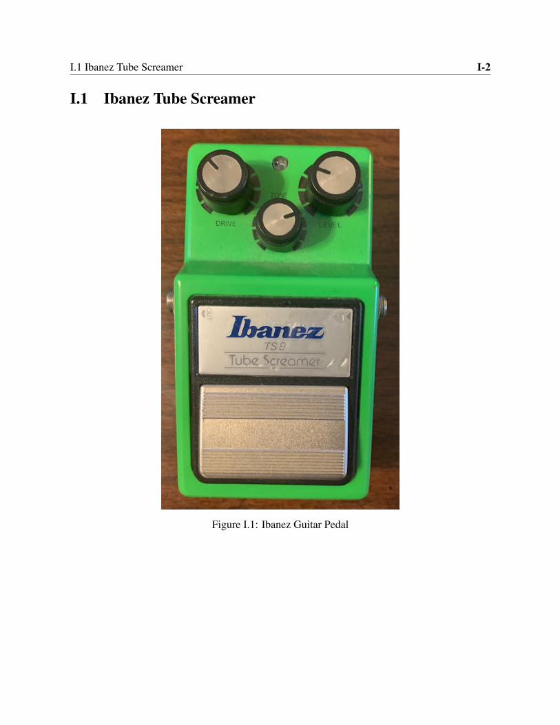
I.1 Ibanez Tube Screamer I-2
I.1 Ibanez Tube Screamer
Figure I.1: Ibanez Guitar Pedal
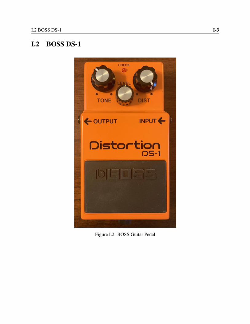
I.2 BOSS DS-1 I-3
I.2 BOSS DS-1
Figure I.2: BOSS Guitar Pedal
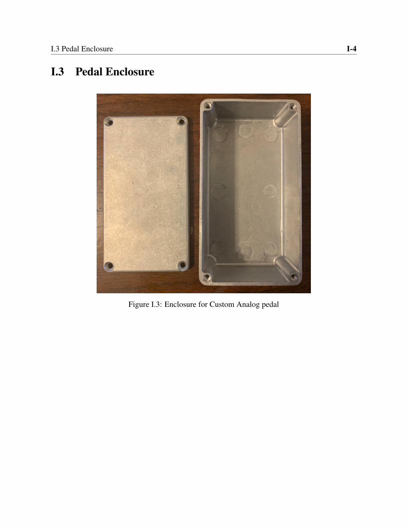
I.3 Pedal Enclosure I-4
I.3 Pedal Enclosure
Figure I.3: Enclosure for Custom Analog pedal


