
John Park ([email protected])
Product Management Director – IC Packaging & Cross-Platform Solutions
This is not your fathers advanced semiconductor packaging…An EDA perspective
© 2020 Cadence Design Systems, Inc. All rights reserved.2
What Is “More Than Moore” and How Does it Impact IC Packaging
Design Flow Challenges for Today’s Advanced Semiconductor Packaging
Summary
Agenda
© 2020 Cadence Design Systems, Inc. All rights reserved.3
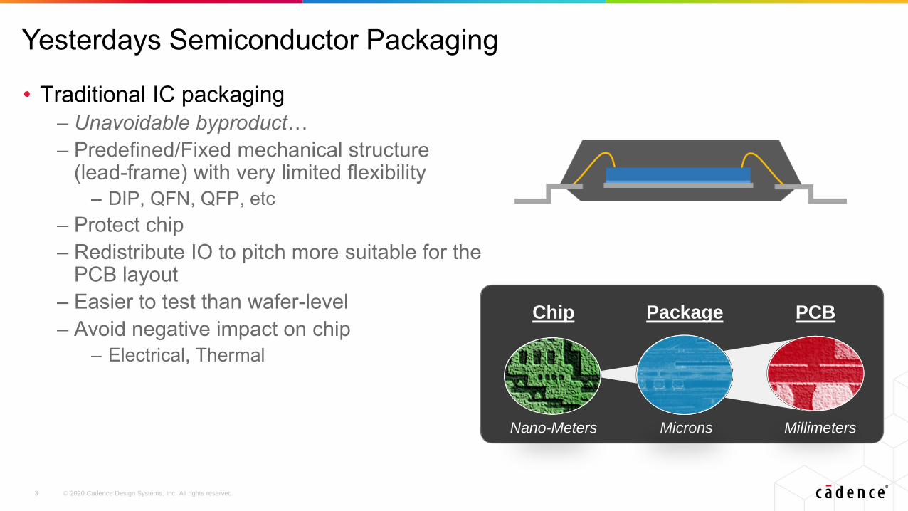
Yesterdays Semiconductor Packaging
Nano-Meters
Chip
Microns
Package
Millimeters
PCB
• Traditional IC packaging
– Unavoidable byproduct…
– Predefined/Fixed mechanical structure (lead-frame) with very limited flexibility
– DIP, QFN, QFP, etc
– Protect chip
– Redistribute IO to pitch more suitable for the PCB layout
– Easier to test than wafer-level
– Avoid negative impact on chip
– Electrical, Thermal
© 2020 Cadence Design Systems, Inc. All rights reserved.4
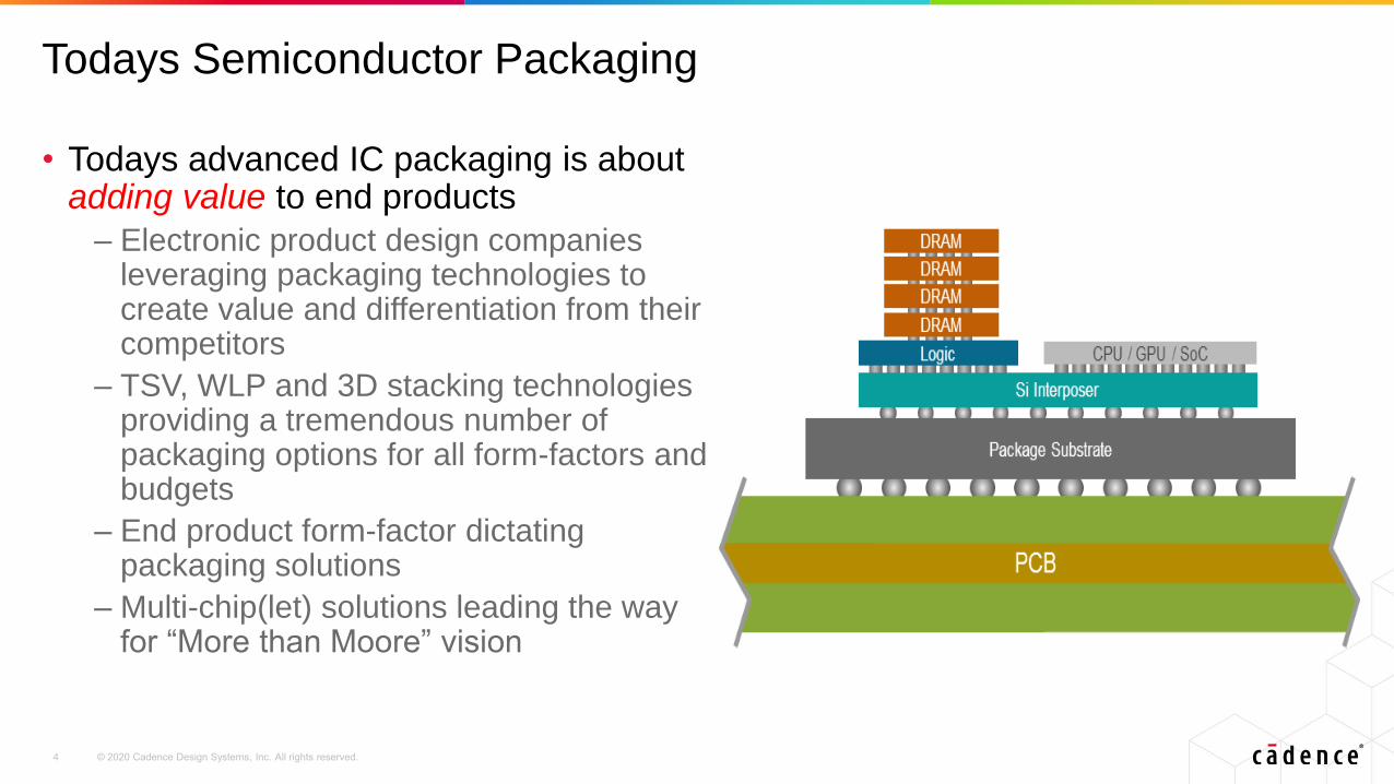
Todays Semiconductor Packaging
• Todays advanced IC packaging is about adding value to end products
– Electronic product design companies leveraging packaging technologies to create value and differentiation from their competitors
– TSV, WLP and 3D stacking technologies providing a tremendous number of packaging options for all form-factors and budgets
– End product form-factor dictating packaging solutions
– Multi-chip(let) solutions leading the way for “More than Moore” vision
© 2020 Cadence Design Systems, Inc. All rights reserved.5
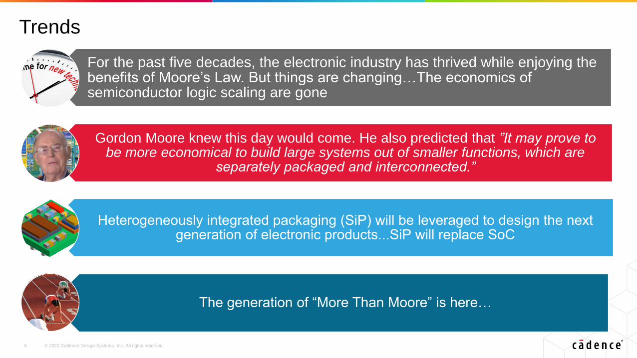
Trends
For the past five decades, the electronic industry has thrived while enjoying the benefits of Moore’s Law. But things are changing…The economics of semiconductor logic scaling are gone
Gordon Moore knew this day would come. He also predicted that ”It may prove to be more economical to build large systems out of smaller functions, which are
separately packaged and interconnected.”
Heterogeneously integrated packaging (SiP) will be leveraged to design the next generation of electronic products...SiP will replace SoC
The generation of “More Than Moore” is here…
© 2020 Cadence Design Systems, Inc. All rights reserved.6
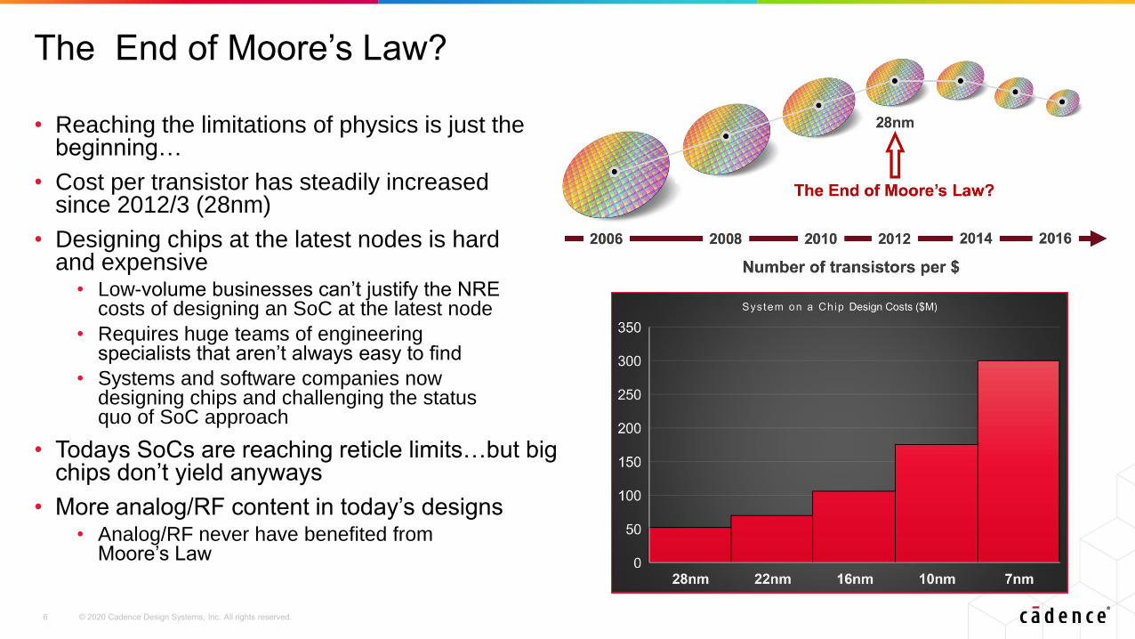
• Reaching the limitations of physics is just the beginning…
• Cost per transistor has steadily increased since 2012/3 (28nm)
• Designing chips at the latest nodes is hard and expensive
• Low-volume businesses can’t justify the NRE costs of designing an SoC at the latest node
• Requires huge teams of engineering specialists that aren’t always easy to find
• Systems and software companies now designing chips and challenging the status quo of SoC approach
• Todays SoCs are reaching reticle limits…but big chips don’t yield anyways
• More analog/RF content in today’s designs • Analog/RF never have benefited from
Moore’s Law
The End of Moore’s Law?
© 2020 Cadence Design Systems, Inc. All rights reserved.7
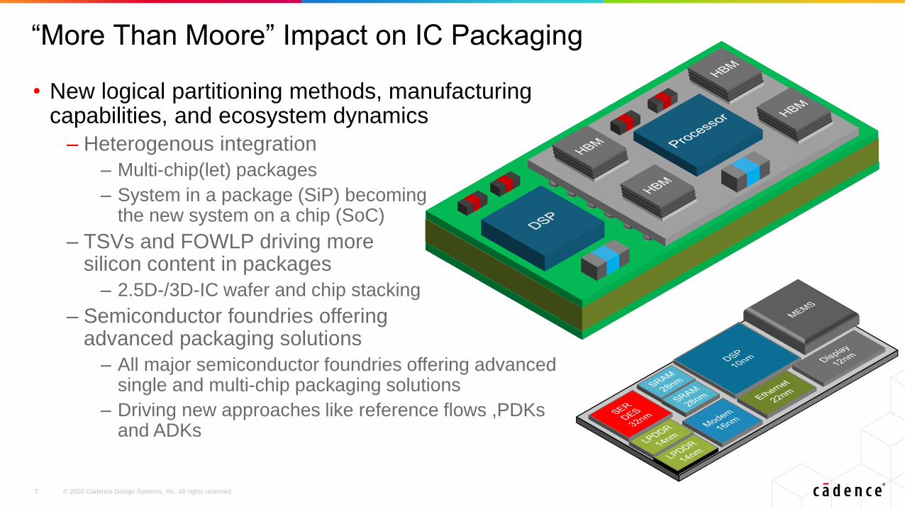
• New logical partitioning methods, manufacturing capabilities, and ecosystem dynamics
– Heterogenous integration
– Multi-chip(let) packages
– System in a package (SiP) becoming the new system on a chip (SoC)
– TSVs and FOWLP driving more silicon content in packages
– 2.5D-/3D-IC wafer and chip stacking
– Semiconductor foundries offering advanced packaging solutions
– All major semiconductor foundries offering advanced single and multi-chip packaging solutions
– Driving new approaches like reference flows ,PDKs and ADKs
“More Than Moore” Impact on IC Packaging
© 2020 Cadence Design Systems, Inc. All rights reserved.8
SerDes
USB
PCIe
CCIX
DDR
VT
Mon
ADC
DAC
PLL
AFE
System
PeriphCamera Secure
DSP
DRAM
Ether Display NAND eMMC
GPU
Application
Processor
Special Sauce
(Custom Logic)SRAM
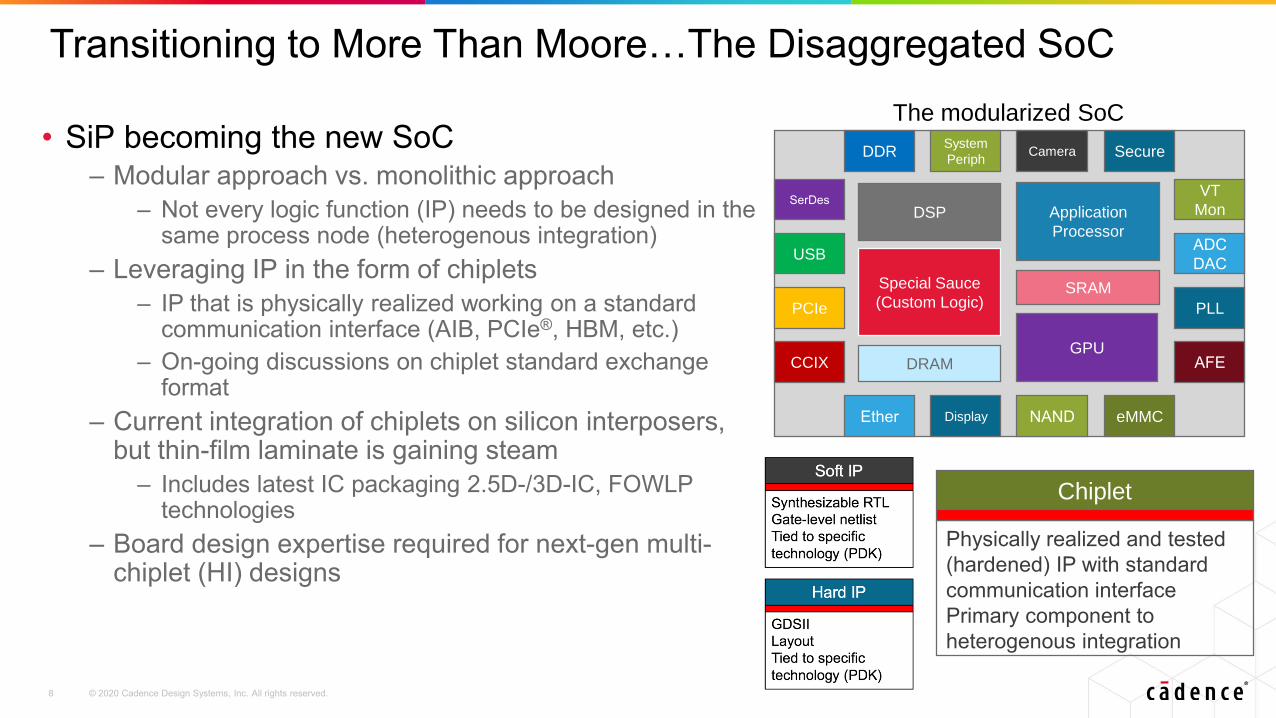
• SiP becoming the new SoC– Modular approach vs. monolithic approach
– Not every logic function (IP) needs to be designed in the same process node (heterogenous integration)
– Leveraging IP in the form of chiplets
– IP that is physically realized working on a standard communication interface (AIB, PCIe®, HBM, etc.)
– On-going discussions on chiplet standard exchange format
– Current integration of chiplets on silicon interposers, but thin-film laminate is gaining steam
– Includes latest IC packaging 2.5D-/3D-IC, FOWLP technologies
– Board design expertise required for next-gen multi-chiplet (HI) designs
Transitioning to More Than Moore…The Disaggregated SoC
Physically realized and tested
(hardened) IP with standard
communication interface
Primary component to
heterogenous integration
Chiplet
The modularized SoC
© 2020 Cadence Design Systems, Inc. All rights reserved.9
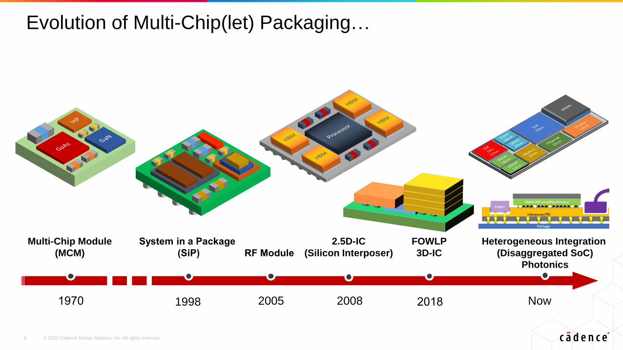
Multi-Chip Module
(MCM) RF Module
Heterogeneous Integration
(Disaggregated SoC)
Photonics
1970 2005 Now
Evolution of Multi-Chip(let) Packaging…
2008
2.5D-IC
(Silicon Interposer)
2018
FOWLP
3D-IC
System in a Package
(SiP)
1998
© 2020 Cadence Design Systems, Inc. All rights reserved.10
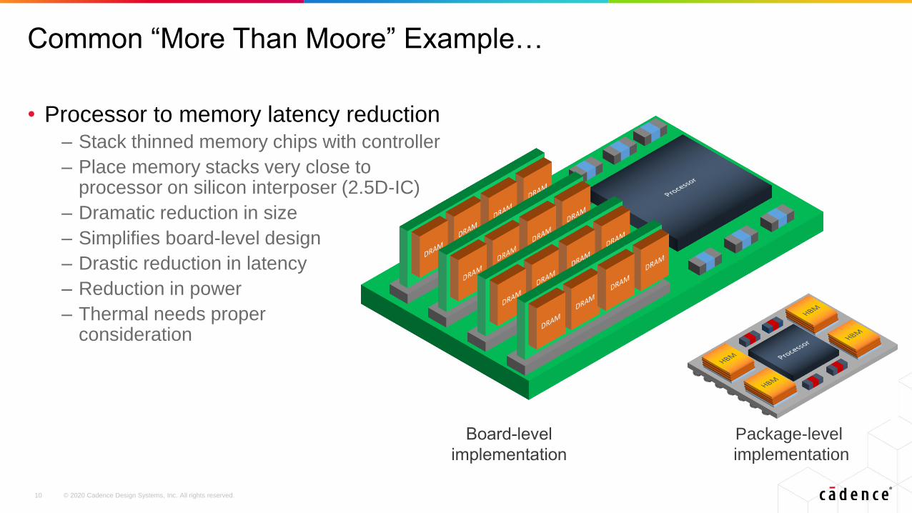
• Processor to memory latency reduction – Stack thinned memory chips with controller
– Place memory stacks very close to processor on silicon interposer (2.5D-IC)
– Dramatic reduction in size
– Simplifies board-level design
– Drastic reduction in latency
– Reduction in power
– Thermal needs proper consideration
Common “More Than Moore” Example…
Board-level
implementation
Package-level
implementation
© 2020 Cadence Design Systems, Inc. All rights reserved.11
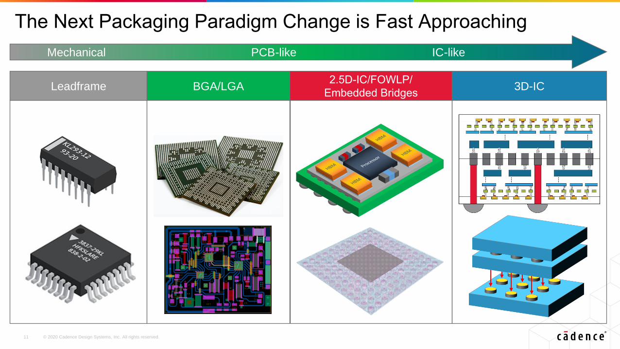
The Next Packaging Paradigm Change is Fast Approaching
Leadframe BGA/LGA 3D-IC2.5D-IC/FOWLP/
Embedded Bridges
Mechanical PCB-like IC-like
© 2020 Cadence Design Systems, Inc. All rights reserved.12
What Is “More Than Moore” and How Does it Impact IC Packaging
Design Flow Challenges for Today’s Advanced Semiconductor Packaging
Summary
Agenda
© 2020 Cadence Design Systems, Inc. All rights reserved.13
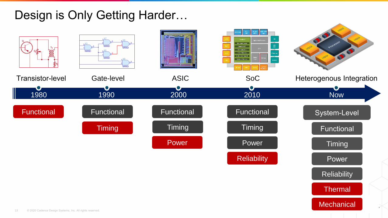
Design is Only Getting Harder…
1980 2000 2010 Now1990
Transistor-level Gate-level ASIC SoC Heterogenous Integration
Functional Functional Functional
Functional
Functional
Timing Timing Timing
TimingPower Power
PowerReliability
Reliability
Thermal
System-Level
Mechanical
© 2020 Cadence Design Systems, Inc. All rights reserved.14
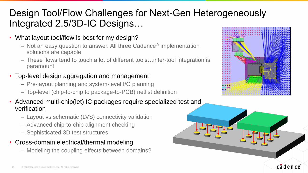
Design Tool/Flow Challenges for Next-Gen Heterogeneously Integrated 2.5/3D-IC Designs…
• What layout tool/flow is best for my design?
– Not an easy question to answer. All three Cadence® implementation solutions are capable
– These flows tend to touch a lot of different tools…inter-tool integration is paramount
• Top-level design aggregation and management
– Pre-layout planning and system-level I/O planning
– Top-level (chip-to-chip to package-to-PCB) netlist definition
• Advanced multi-chip(let) IC packages require specialized test and verification
– Layout vs schematic (LVS) connectivity validation
– Advanced chip-to-chip alignment checking
– Sophisticated 3D test structures
• Cross-domain electrical/thermal modeling
– Modeling the coupling effects between domains?
© 2020 Cadence Design Systems, Inc. All rights reserved.15
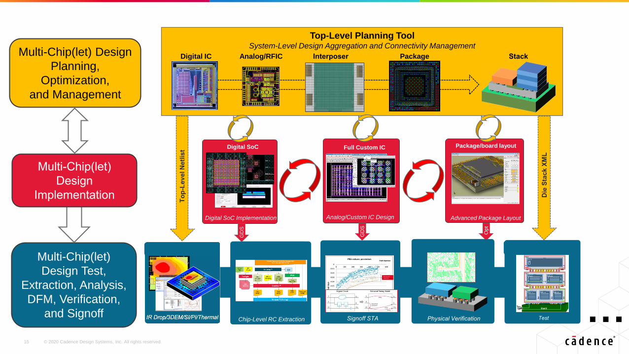
Multi-Chip(let) Design
Planning,
Optimization,
and Management
Multi-Chip(let)
Design Test,
Extraction, Analysis,
DFM, Verification,
and Signoff
Modus
Test
Digital SoC
Digital SoC Implementation
Top-Level Planning ToolSystem-Level Design Aggregation and Connectivity Management
Digital IC Analog/RFIC Interposer Package Stack
Full Custom IC
Analog/Custom IC Design
Package/board layout
Advanced Package Layout
Tempus™
Signoff STA
PVS/Pegasus™
Physical Verification
Quantus™ Extraction
Chip-Level RC Extraction
GD
S
GD
S
Opt
Multi-Chip(let)
Design
Implementation
…
© 2020 Cadence Design Systems, Inc. All rights reserved.16
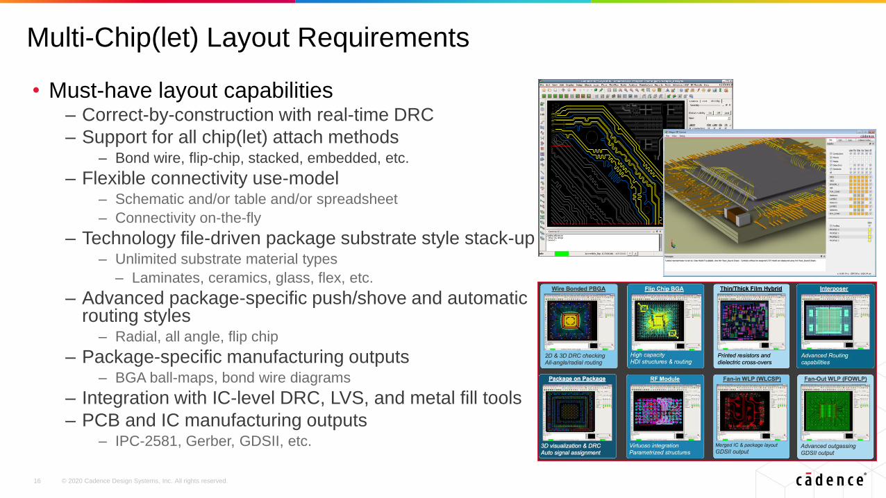
Multi-Chip(let) Layout Requirements
• Must-have layout capabilities– Correct-by-construction with real-time DRC
– Support for all chip(let) attach methods– Bond wire, flip-chip, stacked, embedded, etc.
– Flexible connectivity use-model– Schematic and/or table and/or spreadsheet
– Connectivity on-the-fly
– Technology file-driven package substrate style stack-up – Unlimited substrate material types
– Laminates, ceramics, glass, flex, etc.
– Advanced package-specific push/shove and automaticrouting styles
– Radial, all angle, flip chip
– Package-specific manufacturing outputs– BGA ball-maps, bond wire diagrams
– Integration with IC-level DRC, LVS, and metal fill tools
– PCB and IC manufacturing outputs– IPC-2581, Gerber, GDSII, etc.
© 2020 Cadence Design Systems, Inc. All rights reserved.17
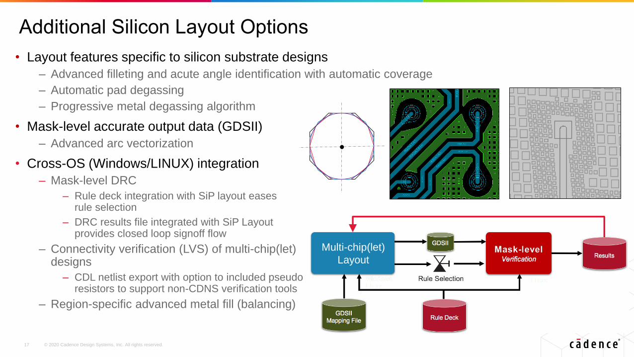
Additional Silicon Layout Options
• Layout features specific to silicon substrate designs
– Advanced filleting and acute angle identification with automatic coverage
– Automatic pad degassing
– Progressive metal degassing algorithm
• Mask-level accurate output data (GDSII)
– Advanced arc vectorization
• Cross-OS (Windows/LINUX) integration
– Mask-level DRC
– Rule deck integration with SiP layout eases rule selection
– DRC results file integrated with SiP Layout provides closed loop signoff flow
– Connectivity verification (LVS) of multi-chip(let) designs
– CDL netlist export with option to included pseudo resistors to support non-CDNS verification tools
– Region-specific advanced metal fill (balancing)
Multi-chip(let)
Layout
© 2020 Cadence Design Systems, Inc. All rights reserved.18
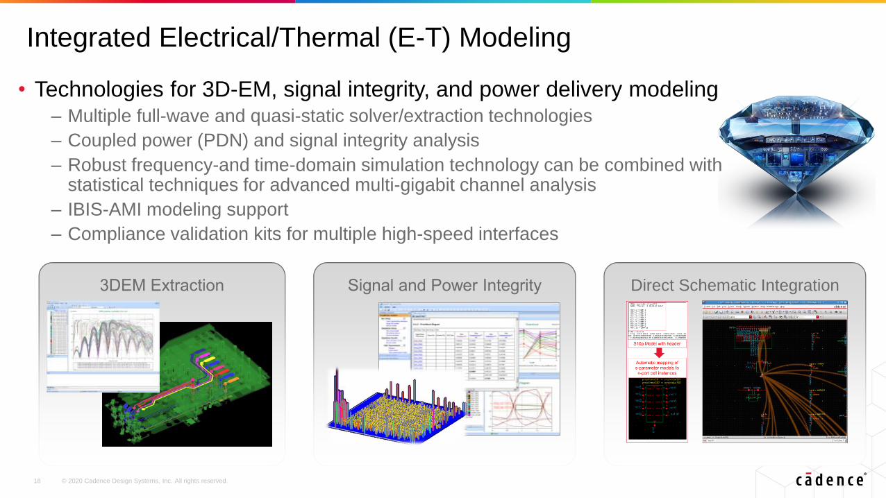
• Technologies for 3D-EM, signal integrity, and power delivery modeling– Multiple full-wave and quasi-static solver/extraction technologies
– Coupled power (PDN) and signal integrity analysis
– Robust frequency-and time-domain simulation technology can be combined with statistical techniques for advanced multi-gigabit channel analysis
– IBIS-AMI modeling support
– Compliance validation kits for multiple high-speed interfaces
Direct Schematic IntegrationSignal and Power Integrity
Integrated Electrical/Thermal (E-T) Modeling
3DEM Extraction
© 2020 Cadence Design Systems, Inc. All rights reserved.19
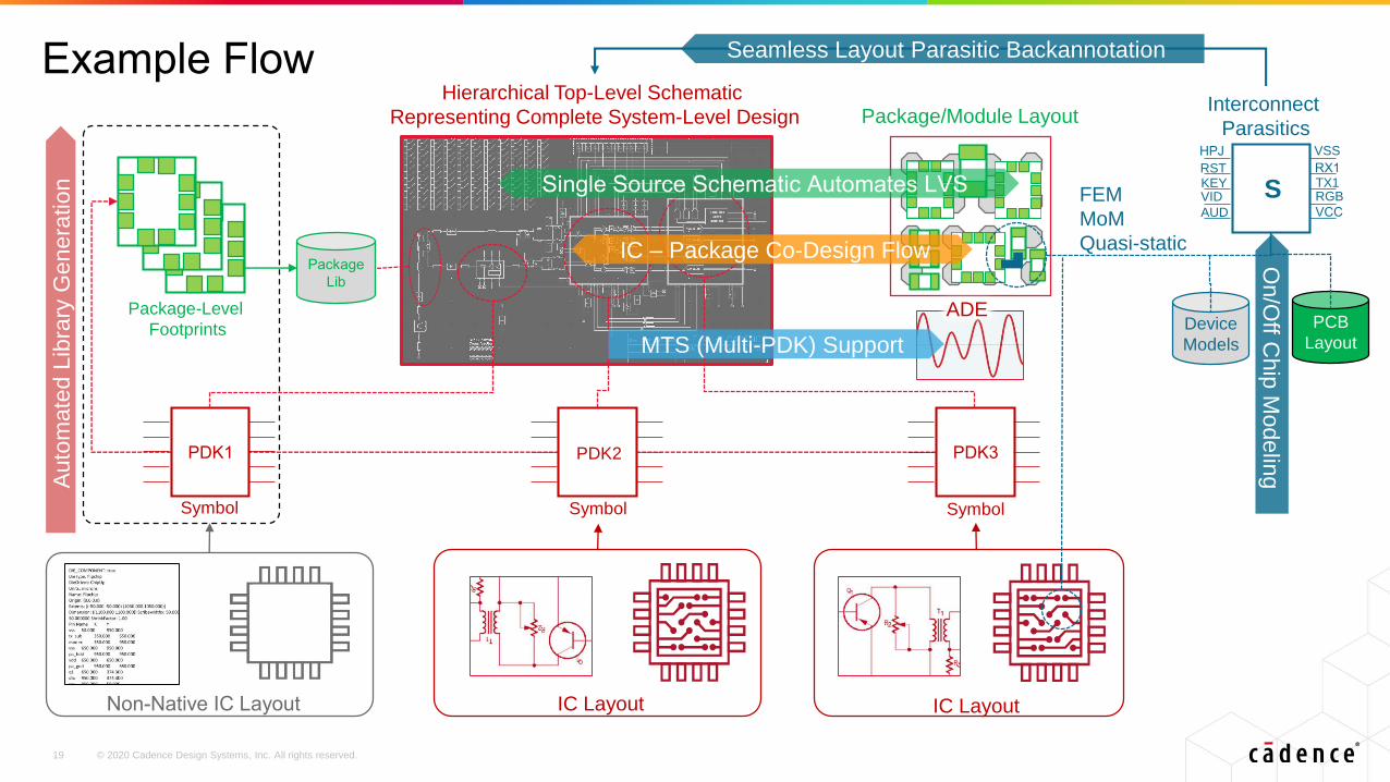
Auto
mate
d L
ibra
ry G
enera
tion
IC Layout IC Layout
PDK3PDK2PDK1
Hierarchical Top-Level Schematic
Representing Complete System-Level Design
Package-Level
Footprints
Symbol Symbol
Package/Module Layout
Non-Native IC Layout
Interconnect
ParasiticsHPJ
RSTKEY
AUD
VID
VSS
RX1TX1
VCC
RGBS
Seamless Layout Parasitic Backannotation
IC – Package Co-Design Flow
Device
Models
Package
Lib
PCB
Layout
Single Source Schematic Automates LVS
MTS (Multi-PDK) Support
Symbol
ADE
FEM
MoM
Quasi-static
On/O
ff Chip
Modelin
g
Example Flow
© 2020 Cadence Design Systems, Inc. All rights reserved.20
What Is “More Than Moore” and How Does it Impact IC Packaging
Design Flow Challenges for Today’s Advanced Semiconductor Packaging
Summary
Agenda
© 2020 Cadence Design Systems, Inc. All rights reserved.21
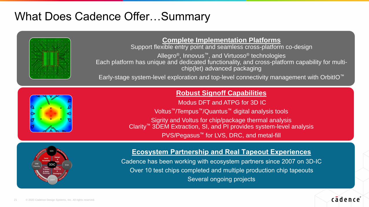
What Does Cadence Offer…Summary
Complete Implementation Platforms Support flexible entry point and seamless cross-platform co-design
Allegro®, Innovus™, and Virtuoso® technologiesEach platform has unique and dedicated functionality, and cross-platform capability for multi-
chip(let) advanced packaging
Early-stage system-level exploration and top-level connectivity management with OrbitIO™
Robust Signoff Capabilities
Modus DFT and ATPG for 3D IC
Voltus™/Tempus™/Quantus™ digital analysis tools
Sigrity and Voltus for chip/package thermal analysisClarity™ 3DEM Extraction, SI, and PI provides system-level analysis
PVS/Pegasus™ for LVS, DRC, and metal-fill
Ecosystem Partnership and Real Tapeout Experiences
Cadence has been working with ecosystem partners since 2007 on 3D-IC
Over 10 test chips completed and multiple production chip tapeouts
Several ongoing projects
© 2020 Cadence Design Systems, Inc. All rights reserved worldwide. Cadence, the Cadence logo, and the other Cadence marks found at www.cadence.com/go/trademarks are trademarks or registered trademarks of Cadence Design
Systems, Inc. Accellera and SystemC are trademarks of Accellera Systems Initiative Inc. All Arm products are registered trademarks or trademarks of Arm Limited (or its subsidiaries) in the US and/or elsewhere. All MIPI
specifications are registered trademarks or service marks owned by MIPI Alliance. All PCI-SIG specifications are registered trademarks or trademarks of PCI-SIG. All other trademarks are the property of their respective owners.


