

MULTIFUNCTIONAL DIGITAL COLOR SYSTEMS
e-STUDIO3511/4511
File No. SME03000500R03042130900-TTECVer02_2004-10

© 2003 TOSHIBA TEC CORPORATION
All rights reserved

• Be sure not to hold the movable parts or units (e.g. the control panel, ADU or RADF) whentransporting the equipment.
• Be sure to use a dedicated outlet with AC 110/13.2A, 115V or 127V/12A, 220V-240V or 240V/8A) for its power source.
• The equipment must be grounded for safety.Never ground it to a gas pipe or a water pipe.
• Select a suitable place for installation.Avoid excessive heat, high humidity, dust, vibration and direct sunlight.
• Also provide proper ventilation as the equipment emits a slight amount of ozone.• To insure adequate working space for the copying operation, keep a minimum clearance of
80 cm (32”) on the left, 80 cm (32”) on the right and 10 cm (4”) in the rear.• The socket-outlet shall be installed near the equipment and shall be easily accessible.
2. Service of Machines• Basically, be sure to turn the main switch off and unplug the power cord during service.• Be sure not to touch high-temperature sections such as the exposure lamp, the fuser unit, the
damp heater and their periphery.• Be sure not to touch high-voltage sections such as the chargers, transfer belt, 2nd transfer roller,
developer, IH control circuit, high-voltage transformer, exposure lamp control inverter, inverterfor the LCD backlight and power supply unit. Especially, the board of these components shouldnot be touched since the electric charge may remain in the capacitors, etc. on them even afterthe power is turned OFF.
• Be sure not to touch rotating/operating sections such as gears, belts, pulleys, fan, etc.• Be careful when removing the covers since there might be the parts with very sharp edges
underneath.• When servicing the machines with the main switch turned on, be sure not to touch live sections
and rotating/operating sections. Avoid exposure to laser radiation.• Use suitable measuring instruments and tools.• Avoid exposure to laser radiation during servicing.
- Avoid direct exposure to the beam.- Do not insert tools, parts, etc. that are reflective into the path of the laser beam.- Remove all watches, rings, bracelets, etc. that are reflective.
• Unplug the power cable and clean the area around the prongs of the plug once a year or more.A fire may occur when dust lies on this area.
GENERAL PRECAUTIONS REGARDING THE INSTALLATIONAND SERVICE FOR e-STUDIO3511/4511
The installation and service should be done by a qualified service technician.
1. Transportation/Installation• When transporting/installing the equipment, employ four persons and be sure to use the positions
as indicated below.The equipment is quite heavy and weighs approximately 112kg (246 lb.), therefore pay full attentionwhen handling it.

3. Main Service Parts for Safety
• The breaker, door switch, fuse, thermostat, thermofuse, thermistor, etc. are particularly important
for safety. Be sure to handle/install them properly. If these parts are shorted circuit and/or made
their functions out, they may burn down, for instance, and may result in fatal accidents. Do not
allow a short circuit to occur. Do not use the parts not recommended by Toshiba TEC Corporation.
4. Cautionary Labels
• During servicing, be sure to check the rating plate and the cautionary labels such as “Unplug the
power cord during service”, “Hot area”, “Laser warning label” etc. to see if there is any dirt on
their surface and whether they are properly stuck to the equipment.
5. Disposition of Consumable Parts, Packing Materials, Used batteries and RAM-ICs
• Regarding the recovery and disposal of the equipment, supplies, consumable parts, packing
materials, used batteries and RAM-ICs including lithium batteries, follow the relevant local
regulations or rules.
6. When parts are disassembled, reassembly is basically the reverse of disassembly unless
otherwise noted in this manual or other related documents. Be careful not to reassemble
small parts such as screws, washers, pins, E-rings, star washers in the wrong places.
7. Basically, the machine should not be operated with any parts removed or disassembled.
8. Precautions Against Static Electricity
• The PC board must be stored in an anti-electrostatic bag and handled carefully using a wristband,
because the ICs on it may become damaged due to static electricity.
Caution: Before using the wristband, pull out the power cord plug of the equipment and
make sure that there are no uninsulated charged objects in the vicinity.
Caution : Dispose of used batteries and RAM-ICs including lithium batteries
according to this manual.
Attention : Se débarrasser de batteries et RAM-ICs usés y compris les batteries
en lithium selon ce manuel.
Vorsicht : Entsorgung des gebrauchten Batterien und RAM-ICs (inklusive
der Lithium-Batterie) nach diesem Handbuch.

November 2003 © TOSHIBA TEC i e-STUDIO3511/4511 CONTENTS
CONTENTS
1. SPECIFICATIONS/ACCESSORIES/OPTIONS/SUPPLIES.......................................... 1-11.1 Specifications ..................................................................................................................... 1-1
1.2 Accessories ........................................................................................................................ 1-5
1.3 Options ............................................................................................................................... 1-6
1.4 Supplies ............................................................................................................................. 1-6
1.5 System List ........................................................................................................................ 1-7
2. OUTLINE OF THE MACHINE ....................................................................................... 2-12.1 Sectional View.................................................................................................................... 2-1
2.2 Electric Parts Layout .......................................................................................................... 2-5
2.3 Symbols and Functions of Various Components.............................................................. 2-14
2.4 General Description ......................................................................................................... 2-21
2.4.1 System block diagram........................................................................................... 2-21
2.4.2 Construction of boards .......................................................................................... 2-22
2.5 Disassembly and Replacement of Covers and PC boards .............................................. 2-25
2.5.1 Covers .................................................................................................................. 2-25
2.5.2 PC boards ............................................................................................................. 2-31
2.5.3 Options ................................................................................................................. 2-36
3. COPY PROCESS .......................................................................................................... 3-13.1 Expression of Colors and 4-Step Copy Process ................................................................ 3-1
3.2 General Description of Copying Process ........................................................................... 3-2
3.3 Details of Copying Process ................................................................................................ 3-3
3.4 List of Copying Process Conditions ................................................................................. 3-10
4. General OPERATION ................................................................................................... 4-14.1 Overview of Operation ....................................................................................................... 4-1
4.2 Description of Operation .................................................................................................... 4-1
4.2.1 Warming-up ............................................................................................................ 4-1
4.2.2 Ready (ready for copying) ....................................................................................... 4-2
4.2.3 Drawer feed copying (Upper drawer paper feeding) ............................................... 4-2
4.2.4 Bypass feed copying ............................................................................................... 4-6
4.2.5 Interruption copying ................................................................................................ 4-6
4.3 Detection of Abnormality .................................................................................................... 4-7
4.3.1 Types of abnormality ............................................................................................... 4-7
4.3.2 Description of abnormality ...................................................................................... 4-7
4.4 Flow Chart ........................................................................................................................ 4-12
4.4.1 Power ON to ready ............................................................................................... 4-12
4.4.2 Automatic feed copying ......................................................................................... 4-14

e-STUDIO3511/4511 CONTENTS ii November 2003 © TOSHIBA TEC
5. CONTROL PANEL ........................................................................................................ 5-15.1 Control Panel and Display Panel ....................................................................................... 5-1
5.2 Items Shown on the Display Panel .................................................................................... 5-2
5.2.1 Display .................................................................................................................... 5-3
5.3 Relation between the Equipment State and Operator’s Operation .................................... 5-8
5.4 Description of Operation .................................................................................................... 5-9
5.4.1 Dot matrix LCD circuit ............................................................................................. 5-9
5.4.2 LED display circuit ................................................................................................ 5-11
5.5 Disassembly and Replacement........................................................................................ 5-12
6. SCANNER ..................................................................................................................... 6-16.1 Function ............................................................................................................................. 6-1
6.2 Construction ....................................................................................................................... 6-2
6.3 Description of Operation .................................................................................................... 6-4
6.3.1 Scan motor ............................................................................................................. 6-4
6.3.2 Scanning drive circuit .............................................................................................. 6-5
6.3.3 Initialization at power-ON ........................................................................................ 6-7
6.4 Control of Exposure Lamp ................................................................................................. 6-8
6.4.1 General description ................................................................................................. 6-8
6.4.2 Exposure lamp ........................................................................................................ 6-9
6.4.3 Control circuit for the exposure lamp .................................................................... 6-10
6.5 General Description of CCD Control ................................................................................ 6-11
6.5.1 Opto-electronic conversion ................................................................................... 6-11
6.5.2 Shading correction ................................................................................................ 6-11
6.6 Automatic Original Size Detection Circuit ......................................................................... 6-12
6.6.1 Principle of original size detection ......................................................................... 6-12
6.6.2 Process of detection of original size ..................................................................... 6-12
6.7 Disassembly and Replacement........................................................................................ 6-16
7. IMAGE PROCESSING .................................................................................................. 7-17.1 General Description ........................................................................................................... 7-1
7.2 Configuration ...................................................................................................................... 7-3
7.3 SYS Board (PWA-F-SYS-350) ........................................................................................... 7-4
7.3.1 Features .................................................................................................................. 7-4
7.3.2 Functions of image processing circuit ..................................................................... 7-5
7.4 LGC Board (PWA-F-LGC-350) ........................................................................................ 7-10
7.4.1 Features ................................................................................................................ 7-10
7.4.2 Functions of image processing circuit ................................................................... 7-10
7.5 Laser Driving PC Board (LDR Board) .............................................................................. 7-10

November 2003 © TOSHIBA TEC iii e-STUDIO3511/4511 CONTENTS
8. LASER OPTICAL UNIT ................................................................................................ 8-18.1 General Description ........................................................................................................... 8-1
8.2 Structure ............................................................................................................................ 8-3
8.3 Laser Diode........................................................................................................................ 8-7
8.4 Laser Unit Cooling Fan ...................................................................................................... 8-8
8.5 Polygonal Motor ................................................................................................................. 8-8
8.6 Disassembly and Replacement.......................................................................................... 8-9
9. DRIVE SYSTEM ............................................................................................................ 9-19.1 General Description ........................................................................................................... 9-1
9.2 Main Motor ......................................................................................................................... 9-2
9.2.1 Construction ............................................................................................................ 9-2
9.2.2 Drive circuit of main motor ...................................................................................... 9-3
9.2.3 Signal level of motor circuit ..................................................................................... 9-3
9.3 Transport Motor .................................................................................................................. 9-4
9.3.1 Construction ............................................................................................................ 9-4
9.3.2 Drive circuit of transport motor ................................................................................ 9-5
9.4 Developer Motor ................................................................................................................ 9-6
9.4.1 Construction ............................................................................................................ 9-6
9.4.2 Drive circuit of developer motor .............................................................................. 9-7
9.5 Disassembly and Replacement.......................................................................................... 9-8
10. PAPER FEEDING SYSTEM ........................................................................................ 10-110.1 General Descriptions ....................................................................................................... 10-1
10.2 Description of Operation .................................................................................................. 10-5
10.2.1 Operation of bypass pickup roller ......................................................................... 10-5
10.2.2 Operation of drawer pickup roller .......................................................................... 10-6
10.2.3 Separation of paper .............................................................................................. 10-7
10.2.4 General operation ................................................................................................. 10-8
10.3 Drive Circuit of Tray-up Motor ........................................................................................ 10-10
10.4 Disassembly and Replacement...................................................................................... 10-11
11. DRUM RELATED SECTION ....................................................................................... 11-111.1 Construction ..................................................................................................................... 11-1
11.2 Functions ......................................................................................................................... 11-2
11.3 Output Control Circuits of High-Voltage Transformer ....................................................... 11-4
11.4 Drum Temperature Detection Circuit ................................................................................ 11-5
11.5 Temperature/Humidity Sensor .......................................................................................... 11-6
11.5.1 General description ............................................................................................... 11-6
11.5.2 Construction .......................................................................................................... 11-6
11.6 Charger Wire Cleaner ...................................................................................................... 11-7
11.6.1 Operation .............................................................................................................. 11-7
11.6.2 Construction .......................................................................................................... 11-7
11.6.3 Drive circuit ........................................................................................................... 11-8
11.7 Disassembly and Replacement........................................................................................ 11-9

e-STUDIO3511/4511 CONTENTS iv November 2003 © TOSHIBA TEC
12. DEVELOPER UNIT ..................................................................................................... 12-112.1 General Description ......................................................................................................... 12-1
12.2 Construction ..................................................................................................................... 12-1
12.3 Sectional View.................................................................................................................. 12-2
12.4 Black Toner Cartridge Drive Unit ...................................................................................... 12-3
12.4.1 General descriptions ............................................................................................. 12-3
12.4.2 Toner motor ........................................................................................................... 12-3
12.5 Black Developer Unit ........................................................................................................ 12-4
12.5.1 Functions .............................................................................................................. 12-4
12.5.2 Black developer unit drive section ........................................................................ 12-5
12.5.3 Black auto-toner sensor circuit .............................................................................. 12-6
12.5.4 Black developer unit lifting mechanism ................................................................. 12-9
12.6 Color Developer Unit ...................................................................................................... 12-10
12.6.1 Functions ............................................................................................................ 12-10
12.6.2 Color developer unit drive section ....................................................................... 12-11
12.6.3 Color auto-toner sensor circuit ............................................................................ 12-12
12.6.4 Color toner supply ............................................................................................... 12-14
12.7 High-Voltage Transformer Output Control Circuit ........................................................... 12-15
12.8 Disassembly and Replacement...................................................................................... 12-16
13. REVOLVER UNIT ........................................................................................................ 13-113.1 General Description ......................................................................................................... 13-1
13.2 Construction ..................................................................................................................... 13-1
13.3 Functions ......................................................................................................................... 13-2
13.4 Drive of Revolver Unit ...................................................................................................... 13-3
13.5 Revolver Motor Drive Circuit ............................................................................................ 13-4
13.5.1 Revolver motor ...................................................................................................... 13-4
13.6 Operation ......................................................................................................................... 13-5
13.6.1 Home position detection ....................................................................................... 13-5
13.6.2 Escape position movement ................................................................................... 13-5
13.6.3 During warming-up................................................................................................ 13-5
13.6.4 During printing....................................................................................................... 13-5
13.6.5 Color toner supply ................................................................................................. 13-6
13.6.6 During image quality control ................................................................................. 13-6
13.7 Disassembly and Replacement........................................................................................ 13-7
14. TRANSFER UNIT ........................................................................................................ 14-114.1 General Descriptions ....................................................................................................... 14-1
14.2 Construction ..................................................................................................................... 14-1
14.3 Functions ......................................................................................................................... 14-2
14.4 Outline of 1st transfer ....................................................................................................... 14-4
14.5 Outline of 2nd transfer ...................................................................................................... 14-4
14.6 High-Voltage Power Supply ............................................................................................. 14-5
14.7 Disassembly and Replacement........................................................................................ 14-6
November 2003 © TOSHIBA TEC v e-STUDIO3511/4511 CONTENTS
15. IMAGE QUALITY CONTROL ..................................................................................... 15-115.1 General Description ......................................................................................................... 15-1
15.2 Principle of the Sensor ..................................................................................................... 15-1
15.3 Flow Chart of Control Procedure ...................................................................................... 15-2
15.4 Construction ..................................................................................................................... 15-3
15.5 Disassembly and Replacement........................................................................................ 15-4
16. FUSER UNIT / PAPER EXIT SECTION ...................................................................... 16-116.1 General Description ......................................................................................................... 16-1
16.2 Operation ......................................................................................................................... 16-1
16.3 Functions ......................................................................................................................... 16-2
16.4 Heater Control Circuit ....................................................................................................... 16-4
16.4.1 Configuration ........................................................................................................ 16-4
16.4.2 Heating principle of IH Heater ............................................................................... 16-5
16.4.3 IH control circuit interface ..................................................................................... 16-6
16.4.4 Relation between system configuration and IH output .......................................... 16-7
16.4.5 Temperature detection section .............................................................................. 16-8
16.4.6 Abnormality in the IH control circuit ..................................................................... 16-13
16.5 Control Circuit of Exit Motor ........................................................................................... 16-15
16.6 Exit Motor Drive.............................................................................................................. 16-15
16.7 Disassembly and Replacement...................................................................................... 16-16
17. AUTOMATIC DUPLEXING UNIT (ADU) ..................................................................... 17-117.1 General Description ......................................................................................................... 17-1
17.2 Description of Operations................................................................................................. 17-2
17.3 Drive of ADU .................................................................................................................... 17-8
17.4 Flow Chart ........................................................................................................................ 17-9
18. POWER SUPPLY UNIT .............................................................................................. 18-118.1 Construction ..................................................................................................................... 18-1
18.2 Operation of DC Output Circuits ...................................................................................... 18-1
18.3 Output Channel ................................................................................................................ 18-2
18.4 Fuse ................................................................................................................................. 18-4
18.5 Configuration of Power Supply Unit ................................................................................. 18-5
18.6 Sequence of Power Supply .............................................................................................. 18-6
18.7 AC Wire Harness ............................................................................................................. 18-7
19. PC BOARDS ............................................................................................................... 19-1

e-STUDIO3511/4511 CONTENTS vi November 2003 © TOSHIBA TEC

November 2003 © TOSHIBA TEC 1 - 1 e-STUDIO3511/4511 SPECIFICATIONS
11. SPECIFICATIONS/ACCESSORIES/OPTIONS/SUPPLIES
1.1 Specifications
Values in [ ] are for e-STUDIO4511 in case that the specification is different between e-STUDIO3511
and e-STUDIO4511.
• Copy process Indirect electrophotographic process (dry)
• Type Desktop type (Console type: when optional Paper Feed Pedestal (PFP) or
optional Large Capacity Feeder (LCF) is installed.)
• Original table Fixed type (the left rear corner used as guide to place originals)
• Accepted originals Sheet, book and 3-dimentional object
For single-sided originals – 50-127 g/m2 (13-34 lb. Bond)
For double-sided originals – 50-105 g/m2 (13-28 lb. Bond)
None of the carbon, bonded nor stapled sheet original is acceptable when
using the optional Reversing Automatic Document Feeder.
Maximum size: A3/LD
• Copy speed (Copies/min.)
e-STUDIO3511
* “–” means “Not acceptable”.
* The copy speed in the above table are available when originals are manually placed for single side,
continuous copying.
* When the Reversing Automatic Document Feeder is used, the copy speed of 35[45] sheets per
minute is only available under the following conditions:
• Original/Mode: Single-sided original/A4/LT size. APS/automatic density are not selected. /Plain
paper.
• Number of sheets: 35[45] or more at the black mode and 11 or more at the color mode.
• Reproduction ratio: 100%
* The values in ( ) are available when printed at color mode.
e-STUDIO4511
Paper supply Paper size
A4, LT, B5
A4-R, B5-R,
A5-R, LT-R, ST-R
B4, LG
A3, LD
Drawer
35 (11)
28 ( 5 )
24 ( 5 )21 ( 5 )
Bypass feed(Size specified)
35 (11)
28 ( 5 )
24 ( 5 )21 ( 5 )
PFP
35 (11)
28 ( 5 )
24 ( 5 )21 ( 5 )
LCF
35 (11)
–
–
–
Paper supply Paper size
A4, LT, B5
A4-R, B5-R,
A5-R, LT-R, ST-R
B4, LG
A3, LD
Drawer
45 (11)
32 ( 5 )
26 ( 5 )22 ( 5 )
Bypass feed(Size specified)
45 (11)
32 ( 5 )
26 ( 5 )22 ( 5 )
PFP
45 (11)
32 ( 5 )
26 ( 5 )22 ( 5 )
LCF
45 (11)
–
–
–

e-STUDIO3511/4511 SPECIFICATIONS 1 - 2 November 2003 © TOSHIBA TEC
1
- The system copy speed is available when 10 sheets of A4/LT size original are set on the RADF
and one of the copy modes in the above table is selected.
- The period of time from pressing [START] to displaying "READY" is the actually measured
value.
- Setting: Automatic exposure OFF, APS/AMS OFF, Text/Photo Mode, feeding from the upper
drawer and Sort Mode.
- The finisher with the saddle stitcher and hole punch unit are not installed.
- The values in ( ) are the speeds at the color modes.
• Copy paper
PFPSize
Weight
Specialpaper
64 to 105 g/m2
17 to 28 lb. Bond
-
Bypass copyA3 to A6-R, LD to ST-R,
13" LG, 8.5"SQ,305 x 457 mm (12" x 18")
(Non-standard or user-specified sizes can be set.)64 to 209 g/m2,17 lb. Bond
to 110 lb. Index(Continuous feeding)
64 to 209 g/m2, 17 lb. Bondto 110 lb. Index
(Single paper feeding)Labels, OHP film(thickness: 80µm or thicker)
A3 to A5-RLD to ST-R, 13" LG,
8.5" SQ
Remarks
Special paper recommended byToshiba Tec
* System copy speed
• First copy time ................... Approx. 6.8 sec. or less (black), approx. 16.2 sec. or less (color)
(A4/LT, upper drawer, 100%, original placed manually)
• Warming-up time ............... Approx. 40 seconds (Stand-alone, temperature: 20°C)
• Multiple copying ................ Up to 999 copies; Key in set numbers
Copy mode
Single-sided originals
↓Single-sided copies
Single-sided originals
↓Double-sided copies
Double-sided originals
↓Double-sided copies
Double-sided originals
↓Single-sided copies
1 set
3 sets
5 sets
1 set
3 sets
5 sets
1 set
3 sets
5 sets
1 set
3 sets
5 sets
Sec.
e-STUDIO3511 e-STUDIO4511
22.9 (70.3)
60.9 (181.8)
94.8 (292.2)
31.3 (95.1)
70.7 (201.8)
110.1 (311.2)
59.6 (149.6)
138.7 (366.6)
217.3 (584.6)
51.2 (124.6)
120.8 (346.5)
188.7 (565.7)
19.8 (70.3)
49.9 (181.8)
76.3 (292.2)
30.3 (95.1)
71.9 (201.8)
101.5 (311.2)
59.5 (149.6)
130.4 (366.6)
201.5 (584.6)
51.5 (124.6)
105.7 (346.5)
158.5 (565.7)
Drawer ADU LCF
A4,LT
04/10

November 2003 © TOSHIBA TEC 1 - 3 e-STUDIO3511/4511 SPECIFICATIONS
1• Reproduction ratio ............. Actual ratio: 100±0.5%
Zooming: 25 - 400% in increments of 1%
(25 - 200% when using RADF)
• Resolution/Gradation ........ Read: 600 dpi
Write: Equivalent to 2400 dpi x 600 dpi (black copy)
Equivalent to 600 dpi x 600 dpi (color copy)
• Eliminated portion ............. Leading edge : 3.0±2.0 mm, Side/trailing edges: 2.0±2.0 mm (black copy)
Leading edge : 5.0±2.0 mm, Side/trailing edges: 2.0±2.0 mm (color copy)
Leading/trailing edges: 5.0±2.0 mm, Side edges: 5.0±2.0 mm (black/color
print)
• Paper feeding .................... Drawers in the equipment – 2 drawers (stack height 60.5 mm, equivalent
to 550 sheets; 64-80 g/m2 (17-22 lb. Bond))
PFP – Option (1 or 2 drawers: stack height 60.5 mm, equivalent to 550
sheets; 64-80 g/m2 (17-22 lb. Bond))
LCF – Option (stack height 137.5 mm x 2, equivalent to 2500 sheets; 64-80
g/m2 (17-22 lb. Bond))
Bypass feed – Stack height 11 mm, equivalent to 100 sheets; 64-80 g/m2
(17-22 lb. Bond)
• Capacity of originals in the Reversing Automatic Document Feeder (Option)
................. A3 to A5-R, LD to ST-R: 100 sheets/80 g/m2 (Stack height 16mm or less)
• Automatic duplexing unit ... Stackless/switchback type
• Toner supply ...................... Automatic toner density detection/supply
Toner cartridge replacing method
• Density control .................. Automatic density mode and manual density mode selectable in 11 steps
• Weight ............................... Approx. 112 kg (246.9 lb.)
• Power requirements .......... AC 110V/13.2A, AC 115V or 127V/15A, 220–240V or 240V/8A (50/60 Hz)
* The acceptable value of each voltage is ±10%.
• Power consumption .......... 1.5 kW or less (100V series), 1.7 kW or less (200V series)
* The electric power is supplied to the reversing automatic document feeder, finisher, PFP and LCF
through the equipment.
• Total counter ...................... Electronical counter

e-STUDIO3511/4511 SPECIFICATIONS 1 - 4 November 2003 © TOSHIBA TEC
1 • Dimensions of the equipment .......... See the figure below (W660 x D718 x H739 mm)
660
718
45°
739
Fig. 1-101
* When the tilt angle of the control panel is 45 degrees.
November 2003 © TOSHIBA TEC 1 - 5 e-STUDIO3511/4511 SPECIFICATIONS
1
Unpacking/Setup instruction 1 set
Operator’s manual 4 pcs. (except for MJD)
Operator's manual pocket 1 pc.
Power cable 1 pc.
Warranty sheet 1 pc. (for NAD)
Setup report 1 set (for NAD and MJD)
Customer satisfaction card 1 pc. (for MJD)
PM sticker 1 pc. (for MJD)
Drum (installed inside of the equipment) 1 pc.
Control panel stopper 1 pc.
Lever 1 pc.
Color developer holder 6 pcs.
Rubber plug 4 pcs.
Blind seal (small / large) 3 pcs. / 1pc.
CD-ROM 4 pcs.
Developer material (Y, M, C, K) 1 pc. each (for TWD)
Screw M3 x 8 / M4 x 8 1 pc. / 1pc.
1.2 Accessories
* Machine version
NAD: North America
MJD: Europe
AUD: Australia
ASD: Asia
TWD: Taiwan
SAD: Saudi Arabia
JPD: Japan

e-STUDIO3511/4511 SPECIFICATIONS 1 - 6 November 2003 © TOSHIBA TEC
1 1.3 Options
Notes:
1. The bridge kit (KN-3511) is necessary for installation of the finisher (MJ-1022, MJ-1023 or
MJ-1024).
2. The finisher (MJ-1023 or MJ-1024) is necessary for installation of the hole punch unit
(MJ-6004N/E/F/S).
3. The PCI slot (GO-1030) is necessary for installation of the scrambler board (GP-1030).
1.4 Supplies
Platen cover KA-3511PC
Reversing Automatic Document Feeder (RADF) MR-3015
Drawer module MY-1021
Paper Feed Pedestal (PFP) KD-1011
Large Capacity Feeder (LCF) KD-1012 A4/LT
Finisher (Hanging type) MJ-1022
Finisher (Console type) MJ-1023, MJ-1024 (with saddle stitcher)
Hole punch unit MJ-6004 N/E/F/S
Staple cartridge STAPLE-1600 (for hanging type)
STAPLE-2000 (for console type)
STAPLE-600 (for saddle stitcher)
Bridge kit KN-3511
Key copy counter, key copy counter socket MU-8, MU-10
Work table KK-3511
Damp heater kit MF-3511
FAX board GD-1150
FAX board 2nd line GD-1160
Expansion memory GC-1180
Wireless LAN adapter GN-1010
PCI slot GO-1030
Scrambler board GP-1030
Drum PS-OD3511
Toner bag PS-TB3511
Toner cartridge (K) PS-ZT3511 *K, PS-ZT3511K
Toner cartridge (Y) PS-ZT3511 *Y, PS-ZT3511Y
Toner cartridge (M) PS-ZT3511 *M, PS-ZT3511M
Toner cartridge (C) PS-ZT3511 *C, PS-ZT3511C
Marked * : E, D, C and T
November 2003 © TOSHIBA TEC 1 - 7 e-STUDIO3511/4511 SPECIFICATIONS
11.5 System List
Fig. 1-501
Rev
ersi
ng A
utom
atic
Doc
umen
t Fee
der
(RA
DF
)M
R-3
015
Pla
ten
cove
r
KA
-351
1PC
Wor
k ta
ble
KK
-351
1
Key
cop
y co
unte
r
MU
8, M
U-1
0
Dam
p he
ater
MF
-351
1
Larg
e C
apac
ity F
eede
r(L
CF
)K
D-1
012A
4/LT
Pap
er F
eed
Ped
esta
l(P
FP
)K
D-1
011
Dra
wer
mod
ule
MY
-102
1S
tapl
e ca
rtrid
geS
TA
PLE
-600
Fin
ishe
r
MJ-
1022
Fin
ishe
r
MJ-
1023
Fin
ishe
r
MJ-
1024
Sta
ple
cart
ridge
ST
AP
LE-2
000
Sta
ple
cart
ridge
ST
AP
LE-1
600
Hol
e pu
nch
unit
MJ-
6004
N/E
/F/S
Brid
ge k
itK
N-3
511
FA
X b
oard
GD
-115
0
FA
X b
oard
2nd
line
GD
-116
0
Exp
ansi
on m
emor
yG
C-1
180
Wire
less
LA
N a
dapt
erG
N-1
010
PC
I slo
tG
O-1
030
Scr
ambl
er b
oard
GP
-103
0

e-STUDIO3511/4511 SPECIFICATIONS 1 - 8 November 2003 © TOSHIBA TEC
1

November 2003 © TOSHIBA TEC 2 - 1 e-STUDIO3511/4511 OUTLINE OF THE MACHINE
2
2. OUTLINE OF THE MACHINE
2.1 Sectional View[A] Front side view
Fig. 2-101
2 9 6 7 5 3 4 8 1 10 11 12
4142
3435
13 1415
16
1718
1920
2122
23
252624
2728
29
32 3130
4433
36
37
3839
40
43
6345
46
47
82
48
49505152
53
55
56
5758
5960
6162
64
65 6667
68 6970
71
71
7273
7475
76
77
78
79
80
81
04/01

e-STUDIO3511/4511 OUTLINE OF THE MACHINE 2 - 2 November 2003 © TOSHIBA TEC
2
1 Original glass
2 RADF original glass
3 Exposure lamp
4 Inverter board
5 Mirror-1
6 Mirror-2
7 Mirror-3
8 Carriage-1
9 Carriage-2
10 Lens
11 CCD board
12 SLG board
13 Laser unit
14 Photoconductive drum
15 Main charger
16 Recovery blade
17 Drum cleaning blade
18 Drum cleaner brush
19 Toner recovery auger
20 Discharge LED
21 Drum thermistor
22 Black developer unit
23 Developer sleeve K
24 Mixer-1 (K)
25 Mixer-2 (K)
26 Black auto-toner sensor
27 Revolver unit
28 Revolver home position sensor
29 Developer unit C
30 Developer sleeve C
31 Mixer-F (C)
32 Mixer-R (C)
33 Developer unit M
34 Developer sleeve M
35 Mixer-F (M)
36 Mixer-R (M)
37 Developer unit Y
38 Developer sleeve Y
39 Mixer-F (Y)
40 Mixer-R (Y)
41 Color auto-toner sensor
42 Color toner cartridge sensor
43 Black toner cartridge
44 Color toner cartridge C
45 Color toner cartridge M
46 Color toner cartridge Y
47 Transfer belt
48 Transfer belt drive roller-1
49 Transfer belt drive roller-2
50 Transfer belt tension roller
51 1st transfer roller
52 Transfer belt cleaning blade
53 2nd transfer roller
55 Fuser roller
56 Pressure roller
57 Fuser belt
58 Separation roller
59 Oil roller
60 Cleaning roller
61 Thermistor
62 Thermostat
63 Exit roller
64 IH coil
65 Upper drawer pickup roller
66 Upper drawer feed roller
67 Upper drawer separation roller
68 Lower drawer pickup roller
69 Lower drawer feed roller
70 Lower drawer separation roller
71 Transport roller
72 Registration roller
73 Bypass pickup roller
74 Bypass feed roller
75 Bypass separation roller
76 Bypass transport roller
77 ADU upper transport roller
78 ADU middle transport roller
79 ADU lower transport roller
80 ADU entrance sensor
81 ADU exit sensor
82 Receiving tray
83 Paper clinging detection sensor
04/01

November 2003 © TOSHIBA TEC 2 - 3 e-STUDIO3511/4511 OUTLINE OF THE MACHINE
2
[B] Rear side view (Drive system)
Fig. 2-102
1 23
4
5
21
20
6
7
8
10
11
12
13
14 1516 9
19
17
18
04/05
e-STUDIO3511/4511 OUTLINE OF THE MACHINE 2 - 4 November 2003 © TOSHIBA TEC
2
1 Scan motor
2 Main motor
3 Drum cleaner brush motor
4 Transport motor
5 Registration clutch
6 Toner motor
7 Upper transport clutch (Low speed)
8 Upper transport clutch (High speed)
9 Black developer drive clutch
10 Lower transport clutch (High speed)
11 Lower transport clutch (Low speed)
12 Upper drawer feed clutch
13 Lower drawer feed clutch
14 Tray-up motor
15 Developer motor
16 Black developer lifting clutch
17 Color developer toner supply clutch
18 Color developer drive clutch
19 Revolver motor
20 ADU motor
21 ADU clutch
04/05

November 2003 © TOSHIBA TEC 2 - 5 e-STUDIO3511/4511 OUTLINE OF THE MACHINE
2
2.2 Electric Parts Layout[A] Unit construction
Fuser unit
Front sideLaser unit
PC board unit
Fig. 2-201
Scanner unit
Drive unit
Control panel unit
Automaticduplexing unit
Bypass unit
Process unit
Paper feeder unit
Transport unit

e-STUDIO3511/4511 OUTLINE OF THE MACHINE 2 - 6 November 2003 © TOSHIBA TEC
2
[B] Scanner unit(B-1) Motor, sensor, lamp
Front side
A4 series
LT series
Front side
Fig. 2-202-1
Fig. 2-202-2
M1
S7S6
EXP
S3S2
S1
S5S4
M14
M1
S7S6
EXP
S3S2
S5S4
M14
M15
M15
November 2003 © TOSHIBA TEC 2 - 7 e-STUDIO3511/4511 OUTLINE OF THE MACHINE
2
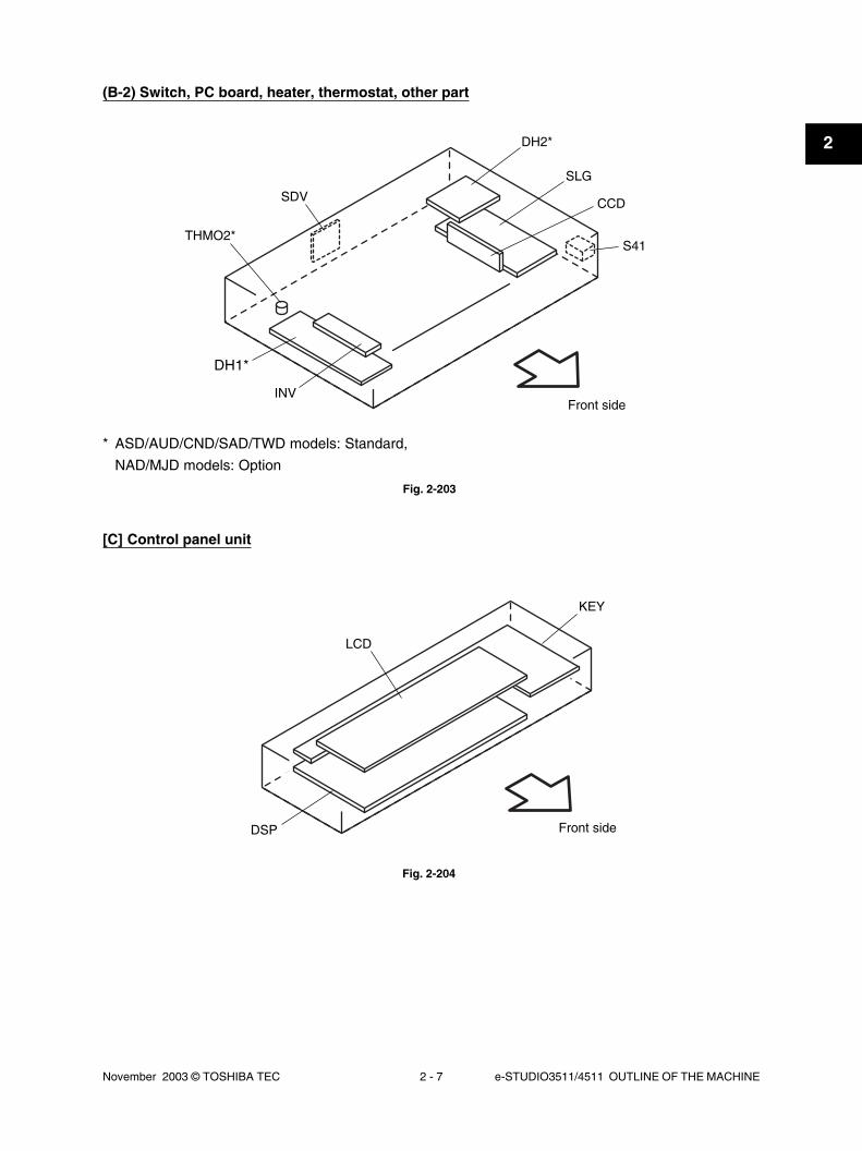
(B-2) Switch, PC board, heater, thermostat, other part
Front side
SDV
INV
THMO2*
DH1*
SLG
S41
CCD
Fig. 2-203
DH2*
* ASD/AUD/CND/SAD/TWD models: Standard,
NAD/MJD models: Option
[C] Control panel unit
Front side
Fig. 2-204
LCD
KEY
DSP

e-STUDIO3511/4511 OUTLINE OF THE MACHINE 2 - 8 November 2003 © TOSHIBA TEC
2
(D-2) Motor, sensor, switch, solenoid, lamp, heater, thermistor, thermostat
Front side
Fig. 2-206
M3
S14
SOL2
S17
ERS
THM4
S13
S20
THMO3*
DH3*
[D] Process unit(D-1) Motor, sensor, switch, clutch, solenoid
Front side
Fig. 2-205
S16
M2CLT1
S10
S9
S8
SOL1
S15
S19
S21
S12
S11
M16
* ASD/AUD/CND/SAD/TWD models: Standard,
NAD/MJD models: Option
M20
S45

November 2003 © TOSHIBA TEC 2 - 9 e-STUDIO3511/4511 OUTLINE OF THE MACHINE
2
[E] Laser unit
Front side
Fig. 2-208
SNS
LDR
M4
(D-3) Motor, switch
S26
S25
M13
Front side
Fig. 2-207

e-STUDIO3511/4511 OUTLINE OF THE MACHINE 2 - 10 November 2003 © TOSHIBA TEC
2
[F] Paper feeder unit
Front side
[G] Transport unit
Fig. 2-209
Fig. 2-210
CLT3
CLT2S31
S33
S32
S34
S27S29
S28
S30
Front side
S18
S22
S44
S24
S23
CLT5
S42
S43
04/05
November 2003 © TOSHIBA TEC 2 - 11 e-STUDIO3511/4511 OUTLINE OF THE MACHINE
2
[H] Bypass unit
Front side
Front side
[I] Automatic duplexing unit
S37 S38
Fig. 2-211
Fig. 2-212
SFB
CLT6
SOL3
S35
S36
ADU
M5
CLT7S39

e-STUDIO3511/4511 OUTLINE OF THE MACHINE 2 - 12 November 2003 © TOSHIBA TEC
2
[J] Fuser unit
Front side
Front side
[K] Drive unit
CLT9
Fig. 2-213
Fig. 2-214
IH-COIL
THM3
THM2
THM1
S40
M12
CLT8
DRV
M18
THMO1
CLT10
M11CLT11
M10CLT16
HVT
M6
CLT15
CLT13
CLT14
M9
CLT12
M8
M7
IH
M17
CCL

November 2003 © TOSHIBA TEC 2 - 13 e-STUDIO3511/4511 OUTLINE OF THE MACHINE
2
Front side
[L] PC board unit
SYS
Fig. 2-215
M19
LGC
PS
FIL or FUS*
BRK
NF
NIC
HDD
* NAD/SAD/TWD models: FIL (Standard),
ASD/AUD/CND models: FUS (Standard),
MJD model: FUS (Option)
05/03
M21

e-STUDIO3511/4511 OUTLINE OF THE MACHINE 2 - 14 November 2003 © TOSHIBA TEC
2P-I
P17 - I8
P31 - I24
P37 - I16
P10 - I10
P42 - I18
P14 - I6
P6 - I15
P14 - I41
P16 - I26
P4 - I26
P15 - I1
P36 - I11
P28 - I35
P11 - I15
P17 - I27
P5 - I22
P8 - I12
P14 - I49
P7 - I9
P1 - I35
P8 - I50
RemarksB-1
D-1
D-2
E
I
K
K
K
K
K
K
K
B-1
D-3
B-1
D-1
K
K
L
D-1
L
NameSCAN-MOTScan motorBELT-CLN-MOTTransfer belt cleaner auger motorTNR-MOTToner motorM/DC-POLPolygonal motorADU-MOTADU motorMAIN-MOTMain motorEXIT-MOTExit motorDRM-CLN-MOTDrum cleaner brush motorTRSP-MOTTransport motor
TRY-MOTTray-up motorDEV-MOTDeveloper motor
REVLV-MOTRevolver motorCCL-MOTCharger cleaner motorSLG-FAN-MOTSLG board cooling fanSCAN-FAN-MOTScanner unit cooling fanLSU-FAN-MOTLaser unit cooling fanIH-FAN-MOTIH control board cooling fanOZN-FAN-MOTOzone exhaust fanPS-FAN-MOTPower supply cooling fanINTRNL-FAN-MOTInternal cooling fanHDD-FAN-MOTHDD cooling fan
FunctionDriving the carriages
Driving the transfer belt used toneraugerSupplying the black toner
Driving the polygonal mirror
Driving the automatic duplexing unit
Driving the drum and transfer belt
Driving the exit roller
Driving the drum cleaner brush andused toner augerDriving the fuser unit, 2nd transferroller, registration roller, transportroller and feed rollerDriving the lifting movement of traysin upper/lower drawerDriving the black/color developer unitDriving the lifting movement of theblack developer unitSupplying the color tonerDriving the transfer belt contact/release movementDriving the revolver unit
Driving the main charger wire cleaner
Cooling down the SLG board
Cooling down the scanner unit
Cooling down the laser unit
Cooling down the IH board and SYSboardExhausting ozone and cooling downthe equipment insideCooling down the power supply unit
Cooling down the equipment inside
Cooling down the HDD
SymbolM1
M2
M3
M4
M5
M6
M7
M8
M9
M10
M11
M12
M13
M14
M15
M16
M17
M18
M19
M20
M21
2.3 Symbols and Functions of Various ComponentsThe column "P-I" shows the page and item number in the parts list.
(1) Motors
05/03

November 2003 © TOSHIBA TEC 2 - 15 e-STUDIO3511/4511 OUTLINE OF THE MACHINE
2Symbol
S1-5
S6
S7
S8
S9
S10
S11
S12
S13
S14
S15
S16
S17
S18
S19
S20
S21
S22
S23
S24
NameAPS 1-3, APS-C, APS-RAutomatic original detection sensorHOME-SNRCarriage home position sensorPLTN-SNRPlaten sensorREVLV-HP-SNRRevolver home position sensorCOLR-TNR-SNRColor toner cartridge sensorCOLR-ATTNR-SNRColor auto-toner sensor
K-DEV-POS-SNRBlack developer contact position detectionsensorK-DEV-TIM-SNRBlack developer contact timing detectionsensorK-ATTNR-SNRBlack auto-toner sensorK-TNR-SWBlack toner cartridge switchTRBLT-HP-SNR1Transfer belt home position sensor-1
TRBLT-HP-SNR2Transfer belt home position sensor-2
TNLVL-SNRImage quality sensorTR2-POS-SNR2nd transfer roller position detectionsensorTEMP/HUMI-SNRTemperature/humidity sensorUSD-TNR-FLL-SNR1Toner bag full detection sensor-1USD-TNR-FLL-SNR2Toner bag full detection sensor-2
RGST-SNRRegistration sensorFED-U-SNRUpper drawer feed sensor
FED-L-SNRLower drawer feed sensor
FunctionOriginal size detection
Carriage home position detection
Opening/closing detection of platencover or RADFHome position detection of therevolver unitDetecting the installation fault of colortoner cartridgeDetecting toner density adhered onthe magnetic roller of the colordeveloper unitDetecting the black developercontact position
Detecting the control of ON/OFFtiming of the black developer liftingclutchDetecting the density of toner in theblack developer unitBlack toner cartridge presence/absence detectionDetecting the rotation position oftransfer belt(for timing of speed switching in thickpaper / OHP film mode)Detecting the rotation position oftransfer belt(for timing of the color image datawriting)Toner amount detection on thetransfer beltDetecting the 2nd transfer rollercontact position
Detecting the temperature andhumidity inside the equipmentDetecting the used toner is full in thetoner bagDetecting the presence/absence ofthe toner bagUsed toner amount detection in thetoner bagDetecting the paper transport at theregistration roller sectionDetecting paper jam and papertransport at upper drawer feedingsectionDetecting paper jam and papertransport at lower drawer feedingsection
P-IS1-4: P11 - I12S5: P11 - I13P11 - I17
P17 - I10
P36 - I102
P36 - I104
P36 - I18
P35 - I17
P35 - I17
P34 - I25
P37 - I12
P29 - I23
P30 - I40
P23 - I24
P12 - I5
P5 - I28
P6 - I11
P32 - I108
P23 - I6
P23 - I6
P24 - I52
RemarksB-1
B-1
B-1
D-1
D-1
D-1
D-1
D-1
D-2
D-2
D-1
D-1
D-2
G
D-1
D-2
D-1
G
G
G
(2) Sensors and switches
e-STUDIO3511/4511 OUTLINE OF THE MACHINE 2 - 16 November 2003 © TOSHIBA TEC
2
SymbolS25
S26
S27
S28
S29
S30
S31
S32
S33
S34
S35
S36
S37
S38
S39
S40
S41
S42
S43
S44
S45
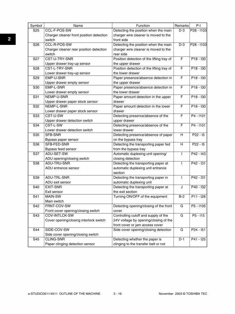
NameCCL-F-POS-SWCharger cleaner front position detectionswitchCCL-R-POS-SWCharger cleaner rear position detectionswitchCST-U-TRY-SNRUpper drawer tray-up sensorCST-L-TRY-SNRLower drawer tray-up sensorEMP-U-SNRUpper drawer empty sensorEMP-L-SNRLower drawer empty sensorNEMP-U-SNRUpper drawer paper stock sensorNEMP-L-SNRLower drawer paper stock sensorCST-U-SWUpper drawer detection switchCST-L-SWLower drawer detection switchSFB-SNRBypass paper sensorSFB-FED-SNRBypass feed sensorADU-SET-SWADU opening/closing switchADU-TRU-SNRADU entrance sensor
ADU-TRL-SNRADU exit sensorEXIT-SNRExit sensorMAIN-SWMain switchFRNT-COV-SWFront cover opening/closing switchCOV-INTLCK-SWCover opening/closing interlock switch
SIDE-COV-SWSide cover opening/closing switchCLING-SNRPaper clinging detection sensor
FunctionDetecting the position when the maincharger wire cleaner is moved to thefront sideDetecting the position when the maincharger wire cleaner is moved to therear sidePosition detection of the lifting tray ofthe upper drawerPosition detection of the lifting tray ofthe lower drawerPaper presence/absence detection inthe upper drawerPaper presence/absence detection inthe lower drawerPaper amount detection in the upperdrawerPaper amount detection in the lowerdrawerDetecting presence/absence of theupper drawerDetecting presence/absence of thelower drawerDetecting presence/absence of paperon the bypass trayDetecting the transporting paper fedfrom the bypass trayAutomatic duplexing unit opening/closing detectionDetecting the transporting paper atautomatic duplexing unit entrancesectionDetecting the transporting paper inautomatic duplexing unitDetecting the transporting paper atthe exit sectionTurning ON/OFF of the equipment
Detecting opening/closing of the frontcoverControlling cutoff and supply of the24V voltage by opening/closing of thefront cover or jam access coverSide cover opening/closing detection
Detecting whether the paper isclinging to the transfer belt or not
P-IRemarksD-3
D-3
F
F
F
F
F
F
F
F
H
H
I
I
I
J
B-2
G
G
G
D-1
P28 - I103
P28 - I103
P18 - I30
P18 - I30
P18 - I30
P18 - I30
P18 - I30
P18 - I30
P4 - I101
P4 - I101
P22 - I5
P22 - I5
P42 - I43
P42 - I31
P42 - I31
P40 - I32
P11 - I28
P5 - I105
P5 - I15
P24 - I51
P41 - I25

November 2003 © TOSHIBA TEC 2 - 17 e-STUDIO3511/4511 OUTLINE OF THE MACHINE
2
(4) Solenoids
(3) Electromagnetic clutches
SymbolCLT1
CLT2
CLT3
CLT5
CLT6
CLT7
CLT8
CLT9
CLT10
CLT11
CLT12
CLT13
CLT14
CLT15
CLT16
NameTRBLT-CLN-CLTTransfer belt cleaner clutchCST-U-FEED-CLTUpper drawer feed clutchCST-L-FEED-CLTLower drawer feed clutch2TR-CONT-CLT2nd transfer roller contact clutchSFB-FEED-CLTBypass feed clutchADU-CLTADU clutchCOLR-DEV-TNR-CLTColor developer toner supply clutchCOLR-DEV-CLTColor developer drive clutchK-DEV-CLTBlack developer drive clutchK-DEV-LIFT-CLTBlack developer lifting clutchRGST-CLTRegistration clutchCST-U-TR-L-CLTUpper transport clutch (Low speed)CST-U-TR-H-CLTUpper transport clutch (High speed)CST-L-TR-L-CLTLower transport clutch (Low speed)CST-L-TR-H-CLTLower transport clutch (High speed)
FunctionDriving the transfer belt cleaningblade contact/release movementDriving the upper drawer pickup roller
Driving the lower drawer pickup roller
Driving the 2nd transfer rollercontact/release movementDriving the bypass pickup roller andbypass feed rollerDriving the automatic duplexing unit
Driving the color developer tonersupply augerDriving the color developer magneticrollerDriving the black developer magneticrollerDriving the black developer liftingcamDriving the registration roller
Driving the upper transport roller(Low speed)Driving the upper transport roller(High speed)Driving the lower transport roller(Low speed)Driving the lower transport roller(High speed)
P-IP31 - I27
P18 - I29
P18 - I29
P12 - I13
P21 - I20
P42 - I16
P15 - I10
P15 - I32
P15 - I28
P15 - I12
P16 - I29
P16 - I19
P16 - I30
P19 - I20
P19 - I16
RemarksD-1
F
F
G
H
I
K
K
K
K
K
K
K
K
K
SymbolSOL1
SOL2
SOL3
NameATTNR-SHUT-SOLColor auto-toner sensor shutter solenoidTNLVL-SHUT-SOLImage quality sensor shutter solenoidSFB-SOLBypass pickup solenoid
FunctionDriving the color auto-toner sensorshutterDriving the image quality sensorshutterDriving the bypass pickup roller
P-IP36 - I25
P23 - I21
P22 - I11
RemarksD-1
D-2
H
04/05

e-STUDIO3511/4511 OUTLINE OF THE MACHINE 2 - 18 November 2003 © TOSHIBA TEC
2
(5) PC boards
SymbolCCD
SLG
SDV
DSP
KEY
LDR
SNS
SFB
ADU
IH
DRV
CCL
SYS
LGC
NIC
FIL
FUS
NamePWA-F-CCDCCD driving PC board (CCD board)PWA-F-SLGScanning section control PC board(SLG board)PWA-F-SDVScan motor driving PC board (SDV board)PWA-F-DSPDisplay PC board (DSP board)PWA-F-KEYKey control PC board (KEY board)PWA-F-LDRLaser driving PC board (LDR board)PWA-F-SNSH-sync signal detection PC board(SNS board)PWA-F-SFBBypass tray slide guide width detectionPC board (SFB board)PWA-F-ADUADU driving PC board (ADU board)PS-IHIH control PC board (IH board)PWA-F-DRVDriving PC board (DRV board)PWA-F-CCLCharger cleaner driving PC board(CCL board)PWA-F-SYSSystem control PC board (SYS board)PWA-F-LGCLogic PC board (LGC board)PWA-F-NICNIC boardPWA-F-FILFilter PC board (FIL board)
PWA-F-FUSFuse PC board (FUS board)
FunctionControlling CCD and A/D conversionof image dataControlling the original scanningsection and RADF
Driving the scan motor
Controlling LCD and the touch panelon the control panelDetecting the button entry andcontrolling LED on the control panelDriving the laser diode
Detection of the laser beam position
Detection of the bypass tray slideguide width
Controlling the automatic duplexingunitControlling each IH coil in the fuserunitControlling each motor and fan in thesystemDriving the charger cleaner motor
Controlling the whole system andimage processingControlling the print engine section
Network connection interface
Cutting noise of the AC powerPower supplying to each dampheater* NAD/SAD/TWD models: StandardPower supplying to each dampheater* ASD/AUD/CND models: Standard* MJD model: Option
P-IP11 - I10
P11 - I38
P17 - I21
P3 - I26
P3 - I25
P10 - I10
P10 - I10
P20 - I13
P42 - I30
P8 - I2
P9 - I8
P9 - I13
P8 - I34
P9 - I7
P8 - I22
P7 - I11
P7 - I4
RemarksB-2
B-2
B-2
C
C
E
E
H
I
K
K
K
L
L
L
L
L
November 2003 © TOSHIBA TEC 2 - 19 e-STUDIO3511/4511 OUTLINE OF THE MACHINE
2
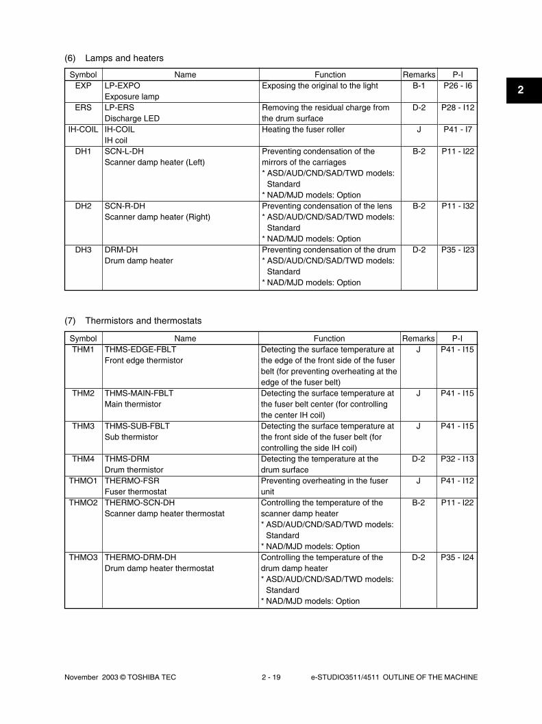
(6) Lamps and heaters
(7) Thermistors and thermostats
SymbolEXP
ERS
IH-COIL
DH1
DH2
DH3
NameLP-EXPOExposure lampLP-ERSDischarge LEDIH-COILIH coilSCN-L-DHScanner damp heater (Left)
SCN-R-DHScanner damp heater (Right)
DRM-DHDrum damp heater
FunctionExposing the original to the light
Removing the residual charge fromthe drum surfaceHeating the fuser roller
Preventing condensation of themirrors of the carriages* ASD/AUD/CND/SAD/TWD models:
Standard* NAD/MJD models: OptionPreventing condensation of the lens* ASD/AUD/CND/SAD/TWD models:
Standard* NAD/MJD models: OptionPreventing condensation of the drum* ASD/AUD/CND/SAD/TWD models:
Standard* NAD/MJD models: Option
P-IP26 - I6
P28 - I12
P41 - I7
P11 - I22
P11 - I32
P35 - I23
RemarksB-1
D-2
J
B-2
B-2
D-2
SymbolTHM1
THM2
THM3
THM4
THMO1
THMO2
THMO3
NameTHMS-EDGE-FBLTFront edge thermistor
THMS-MAIN-FBLTMain thermistor
THMS-SUB-FBLTSub thermistor
THMS-DRMDrum thermistorTHERMO-FSRFuser thermostatTHERMO-SCN-DHScanner damp heater thermostat
THERMO-DRM-DHDrum damp heater thermostat
FunctionDetecting the surface temperature atthe edge of the front side of the fuserbelt (for preventing overheating at theedge of the fuser belt)Detecting the surface temperature atthe fuser belt center (for controllingthe center IH coil)Detecting the surface temperature atthe front side of the fuser belt (forcontrolling the side IH coil)Detecting the temperature at thedrum surfacePreventing overheating in the fuserunitControlling the temperature of thescanner damp heater* ASD/AUD/CND/SAD/TWD models:
Standard* NAD/MJD models: OptionControlling the temperature of thedrum damp heater* ASD/AUD/CND/SAD/TWD models:
Standard* NAD/MJD models: Option
P-IP41 - I15
P41 - I15
P41 - I15
P32 - I13
P41 - I12
P11 - I22
P35 - I24
RemarksJ
J
J
D-2
J
B-2
D-2

e-STUDIO3511/4511 OUTLINE OF THE MACHINE 2 - 20 November 2003 © TOSHIBA TEC
2
(9) Others
SymbolINV
LCD
HDD
PS
NF
BRK
NameINV-EXPInverter boardLCDLCD panelHDDHard diskPS-ACCSwitching power supplyNS-FILTERNoise filterBREAKERBreaker
FunctionControlling the exposure lamp
Displaying and entering eachinformationStoring the program data and imagedataGenerating DC voltage and supplyingit to each section of the equipmentCutting noise of AC power
Preventing the inflow of overcurrentto the equipment
P-IP26 - I7
P3 - I19
P8 - I25
P7 - I9
P7 - I2
P7 - I3
RemarksB-2
C
L
L
L
L
(8) Transformer
SymbolHVT
NamePS-HVTHigh-voltage transformer
FunctionGenerating high-voltage and supplyingit to the following sections• Main charger wire• Main charger grid• Developer bias (color and black)• Transfer bias (1st and 2nd transfer)
P-IP7 - I10
RemarksK

November 2003 © TOSHIBA TEC 2 - 21 e-STUDIO3511/4511 OUTLINE OF THE MACHINE
2
2.4 General Description
2.4.1 System block diagram
LGC
SY
SS
LGC
CD
SN
S
Lase
r un
it
LDR
8
8
168
88
8
16
8
64
6464
16
8
32
32
8
3216
3232
32 3232
32
8 1616
8
PS
TN
Ext
erna
l TE
L
PS
TN
PC
I-bu
s
Dat
a-bu
s
Dat
a-bu
s
Dat
a-bu
s
Dat
a-bu
s
Dat
a-bu
s
Lase
r be
amse
nsor
AS
IC
PW
M
AS
IC
AS
IC
Sys
tem
CP
U33
3MH
z
Imag
e pr
oces
sing
(A
SIC
)
Eng
ine
CP
U24
MH
z
Gat
e ar
ray
#2
AS
IC
AS
IC
AS
IC
Gat
e ar
ray
#1
SR
AM
128K
B
SR
AM
512K
B
NV
RA
M8K
B
NV
RA
M25
6KB
Fla
sh R
OM
512K
B
Fla
sh R
OM
2MB
x 2
Bat
tery
RT
C
Fla
sh R
OM
4MB
x 2
Lase
r di
ode
Dow
nloa
d jig
Dow
nloa
d jig
Dow
nloa
d jig
IPC
PF
P/L
CF
RA
DF
AD
UM
otor
s
HV
TC
lutc
hes
Sen
sors
Sol
enoi
ds
Sw
itche
sB
ypas
sun
it
Key
cou
nter
Cop
y ke
yca
rd
Fin
ishe
r
Brid
ge u
nit
Bus
tran
scei
ver
Bus
tran
scei
ver
Bus
tran
scei
ver
I/O
Fin
ishe
r
Pag
e m
emor
y( D
IMM
)S
tand
ard:
128M
BO
ptio
n:
25
6M
B
Con
trol
pan
el
PCI external slot
Scr
ambl
er b
oard
US
B c
onne
ctor
(de
vice
)
US
B c
onne
ctor
(ho
st)
RS
-232
C
Par
alle
l por
t( I
EE
E-1
284)
HD
D
NC
U( L
INE
-1)
NC
U( L
INE
-2)
NIC
Mod
em
FAX
CC
DA
SIC
LVD
Sre
ceiv
er
Sca
nner
CP
U22
MH
z
Fla
sh R
OM
512K
BS
RA
M12
8KBA
mp
Am
p
Am
p
A/D
A/D
A/D
LVD
Sdr
iver
FAX
Scr
ambl
er b
oard
LAN
con
nect
or( 1
0BA
SE
-T/1
00B
AS
E-T
X)
: Opt
ion
( R)
( G/K
-odd
)
( B/K
-eve
n)
Mai
n m
emor
y( D
IMM
)#0
Stan
dard
: Not
insta
lled
Opt
ion:
128M
B
*Mai
n m
emor
y to
tal
S
tand
ard: 2
56M
B x
1
Opt
ion:
128M
B x
2
Mai
n m
emor
y( D
IMM
)#1
Sta
ndar
d:25
6MB
Opt
ion:
128M
B

e-STUDIO3511/4511 OUTLINE OF THE MACHINE 2 - 22 November 2003 © TOSHIBA TEC
2
2.4.2 Construction of boards(a) Construction diagram of boards
This system consists of the following including the SYS board as a main board.
: DC power supply line
: AC power supply line
: Signal line
AC input
Main switch
Cover opening/closinginterlock switch
SYS
PS-ACCFILor
FUS
LGC
CCD
SDV
INV
SLG
Scanner unit
KEY DSP
Control panelNIC
ADU
SFB
CCL
HVT
DRV
IH
LDR SNS
Laser unit
(b) Function of each boardCCD board:
This is the board to convert the reflected light by the original to electrical signals. It consists of the
CCD, A/D converter, etc. The CCD converts the reflected light by the original to three-color analog
signal; red, green, blue, and the A/D converter converts each analog signal to digital.
SLG board:
This is the board to mainly control the scanning function (scanner unit) and consists of the Scanner-
CPU, ASIC, memory (Flash ROM, SRAM), etc. When scanning the original, the exposure lamp and
scan motor are started by the command from the Scanner-CPU. And the image processing is
performed for the image data sent from the CCD by each ASIC.
SDV board:
This is the board on which the driver for driving the scan motor is mounted. The scan motor is started
by the command from the Scanner-CPU.
INV board:
This is the board on which the lighting control circuit of the exposure lamp is mounted. The exposure
lamp lights by the command from the Scanner-CPU.

November 2003 © TOSHIBA TEC 2 - 23 e-STUDIO3511/4511 OUTLINE OF THE MACHINE
2
DSP board:
This is the board to mainly control the control panel. The Panel processing CPU detecting the input
from each button and touch panel, and the lighting control circuit for the backlight of the LCD are
mounted. And it relays the control signal of the control panel from the SYS board to the LCD and
KEY board.
KEY board:
This is the board on which each button switch and each LED on the control panel are mounted.
LDR board:
This is the board on which the laser diode and the ASIC are mounted. The laser is emitted based on
the output image data signal from the ASIC on the LGC board.
SNS board:
This is the board on which the light sensor for detecting the radiating position of the laser is mounted.
It outputs the H-sync signal to the PWM (Pulse Width Modulator) on the LGC board.
SFB board:
This is the board on which the circuit pattern is printed. It detects the position of the slide guide of the
bypass unit.
CCL board:
This is the board on which the driver for driving the charger cleaner motor is mounted.
ADU board:
This is the board to relay each signal between the ASIC on the LGC board and the electric parts
(motor, sensor, clutch) in the ADU.
IH board:
This is the board to generate the electric power for driving the IH coil of the fuser unit from the AC
electric power input via the switching power supply. And then it is provided.
DRV board:
This is the board on which the driver for driving the revolver motor, exit motor, and each fan motor are
mounted.
SYS board:
This is the main board taking a leading part in all systems. It consists of the System-CPU, ASIC,
memory (DIMM, Flash ROM, SRAM, NVRAM), RTC (Real Time Clock IC) etc. The System-CPU
controls each ASIC to perform the control of the image processing, image memory (page memory,
main memory, HDD), external interface (RS-232C, IEEE-1284, USB, PCI), NIC, and FAX. And based
on the input data from the control panel, System-CPU communicates with Scanner-CPU on the SLG
board and Engine-CPU on the LGC board, and then issues an operation command to the scanner
and printer engine section.

e-STUDIO3511/4511 OUTLINE OF THE MACHINE 2 - 24 November 2003 © TOSHIBA TEC
2
LGC board:
This is the board to mainly control the print function (printer engine). It consists of the Engine-CPU,
ASIC, memory (Flash ROM, SRAM, NVRAM), etc. The Engine-CPU controls each ASIC to drive I/O
(electrical parts) of each section in the system. It leads to the operation of the laser unit, revolver,
developer unit, drum, transfer belt, drawers, bypass unit, ADU, etc. And then the print is made.
NIC board:
This is the interface board to connect this equipment to the LAN environment (10BASE-T, 100BASE-
TX) to communicate with PCs, etc.
FIL board:
This is the board to cut off the noise of AC power from outside, and supply the driving AC power to
the damp heater for condensation prevention of each section (scanner and drum).
FUS board:
This is the board to provide the AC electric power for driving to the damp heater for preventing of the
condensation of each section (scanner and drum).
HVT:
This is the board to generate the DC high voltage from +24V to provide the bias to the section of the
main charger, developer, and transfer.
PS-ACC:
This is the unit to generate each DC voltage, which is used in the equipment, from external AC
electric power input. And then it is provided to each electric part.
November 2003 © TOSHIBA TEC 2 - 25 e-STUDIO3511/4511 OUTLINE OF THE MACHINE
2
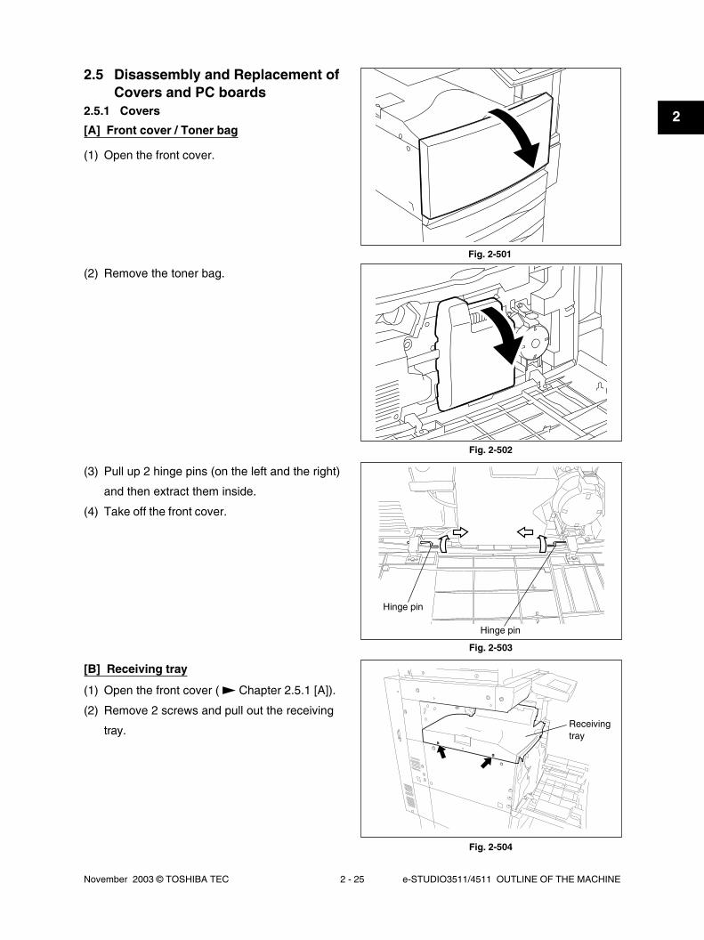
2.5 Disassembly and Replacement ofCovers and PC boards
2.5.1 Covers
[A] Front cover / Toner bag
(1) Open the front cover.
(2) Remove the toner bag.
(3) Pull up 2 hinge pins (on the left and the right)
and then extract them inside.
(4) Take off the front cover.
[B] Receiving tray
(1) Open the front cover ( Chapter 2.5.1 [A]).
(2) Remove 2 screws and pull out the receiving
tray.
Hinge pin
Receivingtray
Fig. 2-502
Fig. 2-504
Fig. 2-501
Fig. 2-503
Hinge pin

e-STUDIO3511/4511 OUTLINE OF THE MACHINE 2 - 26 November 2003 © TOSHIBA TEC
2
[C] Tray back cover
(1) Remove the receiving tray ( Chapter 2.5.1
[B]).
(2) Remove 1 screw and take off the tray back
cover.
[D] Front lower cover
(1) Take off the front cover ( Chapter 2.5.1 [A]).
(2) Take off the black developer unit cover (
Chapter 12.8 (A-1)).
(3) Release 4 latches and take off the front lower
cover.
[E] Front right cover
(1) Take off the front lower cover ( Chapter 2.5.1
[D]).
(2) Remove 2 screws and take off the front right
cover.
[F] Left cover
(1) Open the front cover ( Chapter 2.5.1 [A]).
(2) Remove 4 screws and take off the left cover.
Front lower cover
Front rightcover
Left cover
Fig. 2-505
Fig. 2-506
Fig. 2-507
Fig. 2-508
Latch Latch
Tray back cover
Black developer unit cover

November 2003 © TOSHIBA TEC 2 - 27 e-STUDIO3511/4511 OUTLINE OF THE MACHINE
2
[G] Left rear cover
(1) Remove 2 screws and take off the left rear
cover.
[H] Left upper cover
(1) Remove 2 screws and take off the left upper
cover.
Left rear cover
Left upper cover
Fig. 2-509
Fig. 2-510
[I] Front upper cover
(1) Take off the left upper cover ( Chapter 2.5.1
[H]).
(2) Remove 2 screws. Take off the front upper
cover.
Fig. 2-511
[J] Right upper cover
(1) Remove 3 screws and take off the right upper
cover.
Fig. 2-512

e-STUDIO3511/4511 OUTLINE OF THE MACHINE 2 - 28 November 2003 © TOSHIBA TEC
2
[L] Right rear cover
(1) Open the ADU.
Fig. 2-515
(2) Take off the IH terminal cover ( Chapter
2.5.1 [K]).
(3) Remove 1 screw and take off the ozone filter
cover.
(4) Remove 2 screws and take off the right upper
cover ( Chapter 2.5.1 [J]).
(5) Remove 2 screws and take off the right rear
cover.
Right rearcover
Fig. 2-516
IH terminal cover
Ozone filtercover
(4) Remove 2 screws and take off the IH terminal
cover.
[K] IH terminal cover
Caution:Be sure to unplug before the work, not to get an
electricshock.
(1) Open the ADU.
(2) Open the jam access cover.
(3) Open the fuser unit cover.
IH terminal cover
Fig. 2-513
Fig. 2-514
ADU
Jam access cover
Fuser unit cover

November 2003 © TOSHIBA TEC 2 - 29 e-STUDIO3511/4511 OUTLINE OF THE MACHINE
2
[P] Rear cover
(1) Remove 7 screws and take off the rear cover.
Rear cover
Fig. 2-520
[M] Right lower cover
(1) Take off the right rear hinge cover ( Chapter
2.5.1 [N]).
(2) Remove 2 screws and take off the right lower
cover.
[N] Right rear hinge cover
(1) Remove 2 screws and take off the right rear
hinge cover.
[O] Right front hinge cover
(1) Pull out the upper and lower drawers slightly.
(2) Remove 2 screws and take off the right front
hinge cover.
Right lowercover
Right rear hinge cover
Fig. 2-517
Fig. 2-518
Fig. 2-519
Right front hinge cover
Right rearhinge cover

e-STUDIO3511/4511 OUTLINE OF THE MACHINE 2 - 30 November 2003 © TOSHIBA TEC
2
[Q] Upper rear cover
(1) Take off the ADF or the platen cover.
(2) Take off the left upper cover ( Chapter 2.5.1
[H]).
(3) Take off the right upper cover ( Chapter 2.5.1
[J]).
(4) Remove 2 screws and take off the upper rear
cover.Upper rear cover
Fig. 2-521

November 2003 © TOSHIBA TEC 2 - 31 e-STUDIO3511/4511 OUTLINE OF THE MACHINE
2
2.5.2 PC boardsNote: When the PC board/HDD is replaced, refer to
each CAUTIONS of TROUBLESHOOTHING
in the SERVICE HANDBOOK.
[A] Logic PC board (LGC board)
(A-1) LGC board case
(1) Take off the rear cover ( Chapter 2.5.1 [P]).
(2) Loosen 13 screws and take off the LGC
board cover (plate cover).
(3) Disconnect 20 connectors, release 12
harnesses from harness clamps, remove 5
screws and take off the whole LGC board
with the case.
Fig. 2-522
Fig. 2-523
LGC boardcover
LGC boardcase
(A-2) LGC board
(1) Take off the rear cover ( Chapter 2.5.1 [P]).
(2) Loosen 13 screws and take off the LGC board
cover (plate cover) ( Chapter 2.5.2 (A-1).
(3) Disconnect 20 connectors.
(4) Remove 4 screws and release 2 locking
supports, take off the LGC board.
[B] Hard disk (HDD)
(1) Take off the rear cover ( Chapter 2.5.1 [P]).
(2) Loosen 4 screws and take off the HVT cover.
Fig. 2-525
HVT cover
Fig. 2-524
04/05

e-STUDIO3511/4511 OUTLINE OF THE MACHINE 2 - 32 November 2003 © TOSHIBA TEC
2
(4) Loosen 3 screws, disconnect 2 connectors and
take off the SYS board lower cover.
(5) Remove 4 screws and take off the hard disk
from the SYS board lower cover.
Fig. 2-527
Fig. 2-528
SYS boardlower
Hard disk
Connector
Fig. 2-526
SYS boardupper cover
(3) Loosen 9 screws, disconnect 1 connector
and take off the SYS board upper cover.
[C] System control PC board case
(SYS board case)
(1) Take off the SYS board lower cover
( Chapter 2.5.2 [B]).
(2) Disconnect 5 connectors.
Fig. 2-529
05/03

November 2003 © TOSHIBA TEC 2 - 33 e-STUDIO3511/4511 OUTLINE OF THE MACHINE
2
(3) Remove 4 screws and take off the SYS board
case.
Fig. 2-530
SYS boardcase
Harnessclamp
Connector
Harnessclamp
[D] NIC board / System control PC board
(SYS board)
(1) Take off the SYS board lower cover
( Chapter 2.5.2 [B]).
(2) Disconnect 6 connectors.
Fig. 2-531
Fig. 2-532
(3) Remove 2 screws, release 1 lock support.
Then take off the NIC board.
NIC board
(4) Remove 9 screws, release 1 lock support. Then
take off the SYS board.
Fig. 2-533
SYS board
04/05

e-STUDIO3511/4511 OUTLINE OF THE MACHINE 2 - 34 November 2003 © TOSHIBA TEC
2
(5) Remove 11 screws and take off the cover of
the power supply unit.
[F] High-voltage transformer
(1) Take off the power supply unit
( Chapter 2.5.2 [E]).
(2) Disconnect 8 connectors, remove 2 screws,
release 2 lock supports (white arrow) and
take off the high-voltage transformer.
Fig. 2-536
Fig. 2-537
High-voltage transformer
[E] Power supply unit
(1) Take off the rear cover ( Chapter 2.5.1 [P]).
(2) Disconnect 8 connectors.
(3) Remove 3 screws and take off the whole
switching power supply unit with the bracket.
Note: Be careful not for the power supply unit to
be caught by harnesses.
Fig. 2-534
Power supply unit
(4) Disconnect 1 connector, remove 4 screws and
take off the power supply cooling fan.
FLO
WFig. 2-535
Power supplycooling fan
Connector
04/05

November 2003 © TOSHIBA TEC 2 - 35 e-STUDIO3511/4511 OUTLINE OF THE MACHINE
2
Fig. 2-539
[H] Fuse board (FUS board)
(1) Take off the right rear hinge cover and the right
lower cover ( Chapter 2.5.1 [N] [M]).
(2) Remove 5 screws to take off the unit and turn it
over.
[G] Noise filter
(1) Take off the right rear hinge cover and the right
lower cover ( Chapter 2.5.1 [N] [M]).
(2) Disconnect 4 connectors, remove 1 screw
and take off the noise filter.
Fig. 2-538
White Black
(3) Disconnect 3 connectors and release 4 lock
supports (white arrow) to take off the fuse
board.
Note: FUS board is not included for MJD and NAD.
Fig. 2-540
Fuse board
04/05

e-STUDIO3511/4511 OUTLINE OF THE MACHINE 2 - 36 November 2003 © TOSHIBA TEC
2
Fig. 2-544
(4) Remove 2 screws on the rear side.
Fig. 2-542
[I] Driving PC board (DRV board)
(1) Take off the LGC board case
( Chapter 2.5.2 [A]).
(2) Disconnect 5 connectors, remove 1 screw and
DRV board with the bracket.
Fig. 2-541
DRV board
2.5.3 Options[A] MR-3015 (Reversing Automatic Document
Feeder (RADF))
(1) Turn OFF the power and unplug the power
cable.
(2) Take off the connector cover.
Fig. 2-543
(3) Disconnect the connector.
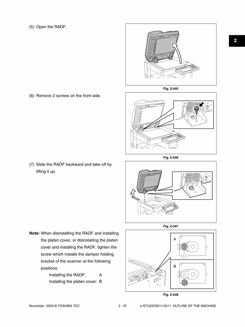
November 2003 © TOSHIBA TEC 2 - 37 e-STUDIO3511/4511 OUTLINE OF THE MACHINE
2
Fig. 2-547
(7) Slide the RADF backward and take off by
lifting it up.
Fig. 2-545
(5) Open the RADF.
(6) Remove 2 screws on the front side.
Fig. 2-546
Note: When disinstalling the RADF and installing
the platen cover, or disinstalling the platen
cover and installing the RADF, tighten the
screw which installs the damper holding
bracket of the scanner at the following
positions.
Installing the RADF: A
Installing the platen cover: B
Fig. 2-548
A
B

e-STUDIO3511/4511 OUTLINE OF THE MACHINE 2 - 38 November 2003 © TOSHIBA TEC
2
(5) Take off the lower drawer of the equipment and
PFP upper drawer.
Fig. 2-552
Fig. 2-550
Fig. 2-551
Fig. 2-549
(3) Remove 1 screw and the ground wire, and then
disconnect 2 connectors (3 if the optional damp
heater is installed).
[B] KD-1011 (Paper Feed Pedestal (PFP))
(1) Turn OFF the power and unplug the power
cable.
(2) Remove 7 screws and take off the rear cover
of the equipment.
Note: Disconnect the connector of the RADF first
when the RADF is installed.
(4) Remove 2 screws and take off 2 fixing brackets
on the rear side.
Connector of optionaldamp heater
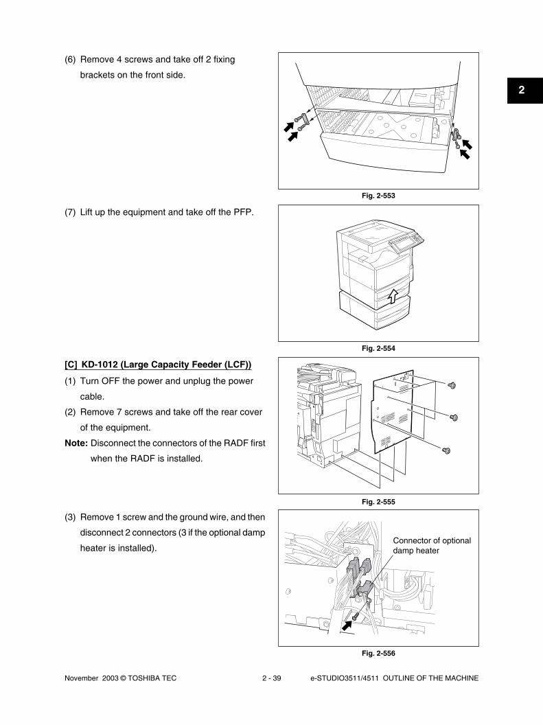
November 2003 © TOSHIBA TEC 2 - 39 e-STUDIO3511/4511 OUTLINE OF THE MACHINE
2
(6) Remove 4 screws and take off 2 fixing
brackets on the front side.
Fig. 2-553
Fig. 2-554
(7) Lift up the equipment and take off the PFP.
Fig. 2-555
[C] KD-1012 (Large Capacity Feeder (LCF))
(1) Turn OFF the power and unplug the power
cable.
(2) Remove 7 screws and take off the rear cover
of the equipment.
Note: Disconnect the connectors of the RADF first
when the RADF is installed.
Fig. 2-556
(3) Remove 1 screw and the ground wire, and then
disconnect 2 connectors (3 if the optional damp
heater is installed).Connector of optionaldamp heater

e-STUDIO3511/4511 OUTLINE OF THE MACHINE 2 - 40 November 2003 © TOSHIBA TEC
2
Fig. 2-560
(7) Remove 4 screws and take off 2 fixing brackets
on the front side.
Fig. 2-558
Fig. 2-559
Fig. 2-557
(4) Remove 2 screws and take off 2 fixing
brackets on the rear side.
(5) Take off the lower drawer of the equipment.
(6) Pull out the LCF drawer.

November 2003 © TOSHIBA TEC 2 - 41 e-STUDIO3511/4511 OUTLINE OF THE MACHINE
2
Fig. 2-561
Fig. 2-562
(8) Lift up the equipment and take off the LCF.
[D] MJ-1022 (Hanging finisher)
<When PFP/LCF is not installed>
(1) Turn OFF the power and unplug the power
cable.
(2) Take off the connector cover and disconnect
the connector.
Fig. 2-563
(3) Remove 2 screws and take off the safety
bracket on the rear side and the cover.
Fig. 2-564
(4) Remove 2 screws and take off the safety
bracket on the front side and the cover.

e-STUDIO3511/4511 OUTLINE OF THE MACHINE 2 - 42 November 2003 © TOSHIBA TEC
2
Fig. 2-568
(3) Remove 2 screws and take off the cover on
the rear side.
Fig. 2-566
Fig. 2-567
Fig. 2-565
(5) Remove 2 screws.
(6) Lift up the finisher and take it off.
<When PFP/LCF is installed>
(1) Turn OFF the power and unplug the power
cable.
(2) Take off the connector cover and disconnect
the connector.

November 2003 © TOSHIBA TEC 2 - 43 e-STUDIO3511/4511 OUTLINE OF THE MACHINE
2
Fig. 2-569
Fig. 2-570
(4) Remove 2 screws and take off the cover on
the front side.
(5) Remove 2 screws.
Fig. 2-571
(6) Lift up the finisher and take it off.
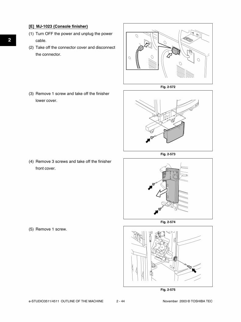
e-STUDIO3511/4511 OUTLINE OF THE MACHINE 2 - 44 November 2003 © TOSHIBA TEC
2
Fig. 2-574
Fig. 2-575
Fig. 2-572
Fig. 2-573
[E] MJ-1023 (Console finisher)
(1) Turn OFF the power and unplug the power
cable.
(2) Take off the connector cover and disconnect
the connector.
(3) Remove 1 screw and take off the finisher
lower cover.
(4) Remove 3 screws and take off the finisher
front cover.
(5) Remove 1 screw.

November 2003 © TOSHIBA TEC 2 - 45 e-STUDIO3511/4511 OUTLINE OF THE MACHINE
2
Fig. 2-577
Fig. 2-578
(7) Remove 1 screw.
(8) Take off the finisher.
Note: Be careful not to fell the finisher when
moving the finisher unit only.
Fig. 2-579
[F] MJ-1024 (Console finisher)
(1) Turn OFF the power and unplug the power
cable.
(2) Take off the connector cover and disconnect
the connector.
Fig. 2-576
(6) Remove 1 screw and take off the cover of the
finisher rear side.

e-STUDIO3511/4511 OUTLINE OF THE MACHINE 2 - 46 November 2003 © TOSHIBA TEC
2
Fig. 2-582
Fig. 2-583
Fig. 2-580
Fig. 2-581
(6) Take off the finisher.
Note: Be careful not to fell the finisher when
moving the finisher unit only.
(3) Open the finisher front cover and remove 1
screw.
(4) Remove 1 screw and take off the cover of the
finisher rear side.
(5) Remove 1 screw.

November 2003 © TOSHIBA TEC 2 - 47 e-STUDIO3511/4511 OUTLINE OF THE MACHINE
2
Fig. 2-585
Fig. 2-586
(3) Open the front cover of the hole punch unit
and remove 1 screw.
(4) Take off the cover of the punch unit lower
side.
Fig. 2-587
(5) Remove 1 screw.
Fig. 2-584
[G] MJ-6004 (Hole punch unit)
(1) Turn OFF the power and unplug the power
cable.
(2) Take off the connector cover and disconnect
connector.

e-STUDIO3511/4511 OUTLINE OF THE MACHINE 2 - 48 November 2003 © TOSHIBA TEC
2
Fig. 2-590
Fig. 2-591
Fig. 2-589
(8) Take off the finisher with the hole punch unit.
Note: Be careful not to fell the finisher when
moving the finisher unit only.
(7) Remove 1 screw.
(9) Disconnect 2 connectors.
Fig. 2-588
(6) Remove 3 screws and take off the punch unit
rear cover.

November 2003 © TOSHIBA TEC 2 - 49 e-STUDIO3511/4511 OUTLINE OF THE MACHINE
2
Fig. 2-593
Fig. 2-594
[H] KN-3511 (Bridge unit)
(1) Turn OFF the power and unplug the power
cable.
(2) Remove 2 screws and take off the cover.
(11) Lift up the punch unit and take it off.
Fig. 2-595
(3) Disconnect 1 connector.
Fig. 2-592
(10) Remove 2 screws.

e-STUDIO3511/4511 OUTLINE OF THE MACHINE 2 - 50 November 2003 © TOSHIBA TEC
2
(7) Lift up the bridge unit and release the hook.
Take off the bridge unit toward the front.
Fig. 2-598
Fig. 2-599
Fig. 2-596
Fig. 2-597
(4) Open the bridge unit. Remove 1 screw and
take off the cover.
(5) Close the bridge unit and remove 1 screw.
(6) Remove 4 screws and take off the bracket.

November 2003 © TOSHIBA TEC 3 - 1 e-STUDIO3511/4511 COPY PROCESS
3
3. COPY PROCESS
3.1 Expression of Colors and 4-Step Copy ProcessA variety of colors can be expressed by mixing the
three primary colors : Yellow, magenta and cyan.
Red can be created by mixing yellow and magenta;
blue can be created by mixing magenta and cyan;
green is created by mixing cyan and yellow; and
mixing all the three primary colors allows you to
obtain black.
This equipment has accomplished to improve
reproducibility by adding black toner to the mixture
of the above three colors at proper ratio.
e-STUDIO3511/4511 adopts a revolver mechanism which combines the three developer units of yellow,
magenta and cyan. In this process, each image of cyan, magenta and yellow is developed in order by
rotating these developers and overlaid on the transfer belt one after another. Then the black image
developed by independent black developer unit is overlaid for the best expressions of colors. Four layers
of color image (K→ C→ M→ Y) on the transfer belt are transferred onto paper.
[Three primary colors]
Yellow
Red
Black
Green
MagentaBlue
Cyan
Fig. 3-101
Fig. 3-102
1st transfer roller
Transfer belt
Fuser unit
2nd transfer roller
Main charger
Photoconductive drum
Black developerunit
Laser optical unit
Color developer unit
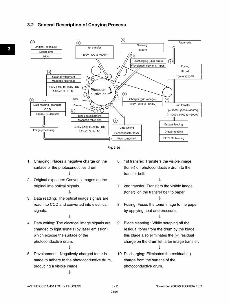
e-STUDIO3511/4511 COPY PROCESS 3 - 2 November 2003 © TOSHIBA TEC
3
2
3 7
4
5-2
8
5-1
1
9
10
6
Original exposure
Xenon lamp
16 W
Data reading (scanning)
CCD
600dpi, 7450 pixels
Image processingData writing
Semiconductor laser
Pw=4.0 nJ/mm2
Discharging (LED array)
Wavelength 660nm x 14pcs.
Charger (grid voltage)
Cleaning
-1000 V
Fusing
IH coil
700 to 1300 W
Paper exit
2nd transfer
(+)1000V (500 to 4800V)
(-)-1000V (-100 to –2000V)
Bypass feeding
PFP/LCF feeding
Drawer feeding
Color developmentMagnetic roller bias
-400V (-100 to -900V) DC
1.0 kV/10kHz AC
Carrier
Toner
3.2 General Description of Copying Process
1. Charging: Places a negative charge on the
surface of the photoconductive drum.
↓2. Original exposure: Converts images on the
original into optical signals.
↓3. Data reading: The optical image signals are
read into CCD and converted into electrical
signals.
↓4. Data writing: The electrical image signals are
changed to light signals (by laser emission)
which expose the surface of the
photoconductive drum.
↓5. Development: Negatively-charged toner is
made to adhere to the photoconductive drum,
producing a visible image.
↓
6. 1st transfer: Transfers the visible image
(toner) on photoconductive drum to the
transfer belt.
↓7. 2nd transfer: Transfers the visible image
(toner) on the transfer belt to paper.
↓8. Fusing: Fuses the toner image to the paper
by applying heat and pressure.
↓9. Blade cleaning : While scraping off the
residual toner from the drum by the blade,
this blade also eliminates the (+) residual
charge on the drum left after image transfer.
↓10. Discharging: Eliminates the residual (–)
charge from the surface of the
photoconductive drum.
Photocon-ductive drum
1800V (400 to 4000V)
1st transfer
Black development
Magnetic roller bias
-400V (-100 to -900V) DC
1.2 kV/10kHz AC
-600V (-300 to -1200V)
Fig. 3-201
04/01

November 2003 © TOSHIBA TEC 3 - 3 e-STUDIO3511/4511 COPY PROCESS
3
3.3 Details of Copying Process(1) Photoconductive drum
The photoconductive drum consists of two layers.
The outer layer is a photoconductive layer made of
an organic photoconductive carrier (OPC), and the
inner layer is an aluminum conductive base in a
cylindrical form.
The photoconductive carrier has a special property:
when it is exposed to light, the electrical resistance
it possesses increases or decreases with the
strength of the light.
Example:
· Strong incident light→
Decreases resistance (works as a conductor.)
· Weak incident light→
Increases resistance (works as an insulator.)
[Formation of electrostatic latent images]
In the processes of charging, data reading, data
writing, and discharging described below, the areas
on the drum corresponding to colored areas on the
original are deprived of negative charge, while the
areas on the drum corresponding to white areas
retain the negative charge. Thus it forms a negative
charge image on the drum surface.
As this negative charge image on the drum is not
visible to the human eye, it is called an “electrostatic
latent image.”
(2) Charging
Charging is a process to apply charge evenly to
the drum surface.
The charger wire produces negative corona
discharge, which is controlled by the grid so that
the drum surface is evenly charged with negative
potential.
The surface potential on the drum is determined
by the grid potential and is controlled to a fixed value
by the grid control circuit.
0
- 500
- 1000
Photoconductive layer
Base
Structure of the photoconductive drum(Example of OPC)
Time (t)
Colored area of original
White area of original
Sur
face
pot
entia
l (V
)
Discharge
process
Charging
process
Electric potential of the photoconductive drum
Main charger
Rotation of drum
Grid control circuit High-voltagetransformer
Fig. 3-301
Fig. 3-302
Fig. 3-303

e-STUDIO3511/4511 COPY PROCESS 3 - 4 November 2003 © TOSHIBA TEC
3CCD board
Scanning sectioncontrol PC board
Image processingsection
(Example)
CCD lightreceivingamount
Value of imagesignals to be
output
Light 255
Dark 0
Difference between"light " and "dark" isdivided into 256 steps.
Imageprocessing
section
Laser drivingPC board
Semiconductorlaser element
Polygonal mirror
(4) Data writing
Data writing is a process of converting the image
signals transmitted from the image processing
section into light signals and exposing the drum
surface with the light signal.
Namely, the image signals transmitted from the
image processing section are converted into optical
signals (laser emission) by the semiconductor laser
element, which are then used to expose the drum
surface, thus forming an electrostatic latent image
there.
(3) Data reading (scanning)
Data reading is a process of illuminating the original
with light and converting the reflected light into
electrical signals.
The light reflected from the original is directed to
the Charge Coupled Device (CCD) and this optical
image information is converted to electrical signals
(image signals), which are then transmitted to the
image processing section via the scanner control
PC board.
The CCD for color processing has RGB filters
provided over its surface, which allow the CCD to
read the light amount in the respective ranges of
wavelength. The image data corresponding to the
respective RGB colors is then transmitted to the
image processing section.
Drum
Fig. 3-304
Fig. 3-305

November 2003 © TOSHIBA TEC 3 - 5 e-STUDIO3511/4511 COPY PROCESS
3
Magnet
Magnetic roller Toner
Carrier (always attractedonto the magnet)
Toner
Photocon-ductive drum
Photoconductive layer
Aluminum base
0
- 100V
- 200V
- 300V
- 500V
- 400V
(5) Development
Development is a process of making the
electrostatic latent images visible to the eye
(visible image).
Developer material is supplied to the
photoconductive drum surface by means of a
magnetic roller, allowing the toner in the
developer material to adhere to the areas on the
drum surface where the potential is lower than
the developer bias which is applied to the
magnetic roller (reverse development).
Drum
White background Halftone Solid
White backgroundImage is notdeveloped
BiasvoltageImage is developed by
toner
When the (–) potential ofthe photoconductive drumis higher than thedeveloper bias.
When the (–) potential ofthe photoconductive drumis lower than thedeveloper bias.
Toner
Magnetic roller
Bias voltage-400V (-100 to -900V) DC1.2kV/10kHz AC
Fig. 3-306
Fig. 3-307
Fig. 3-308
04/01

e-STUDIO3511/4511 COPY PROCESS 3 - 6 November 2003 © TOSHIBA TEC
3
• About developer material
The developer material is comprised of a mixture
of toner and carrier. The toner is charged to a
negative polarity and the carrier to a positive
polarity, due to the friction with each other
caused by mixing.
Toner : Mainly consists of resin and coloring.
Carrier: Consists of ferrite, and over its surface
resin coating to provide consistent frictional
electrification.
N
S
S
[Toner]Ferrite
[Carrier]
Note:
If the developer material is used for a long period
of time (beyond its normal life span), toner will
become caked onto the carrier.
The performance of the carrier is lowered.
Result: 1. Image density is lowered.
2. Toner scattering occurs.
3. Background fogging occurs.
Solution: Replace the developer material.
TonerCarrier
Where toner is caked, nofrictional electrificationoccurs.
• Magnetic roller
- Magnetic brush development technique -
Inside magnetic rollers, the south and north poles
are arranged as shown in the right figure. The
developer material forms a brush-like fluff which
contacts the photoconductive drum surface.
This is caused by the lines of magnetic force
between the south and north poles.
Lines of magnetic force
Magnetic roller
Photoconductivedrum
Fig. 3-309
Fig. 3-310
Fig. 3-311
→
→
Coloring agent(5-10%)
5-13µm
Resin (90-95%)
30-100µm

November 2003 © TOSHIBA TEC 3 - 7 e-STUDIO3511/4511 COPY PROCESS
3
(6) 1st transfer
• 1st transfer is a process of transcribing the
toner image (visible image) formed on the
photoconductive drum to the transfer belt. A
positive bias is applied to the transfer roller,
causing the transfer belt to be positively
charged. This in turn helps to form an electric
field E between the transfer belt (positive) and
the photoconductive layer of the
photoconductive drum (grounded), thus making
the toner image transferred to the transfer belt.
In the copy process of this equipment, images
are transferred in the order of K→C→M→Y on
the transfer belt.
(7) 2nd transfer
• An electrostatic attracting force occurs between
the polarized charge (negative) on the lower
surface of transfer belt and the belt itself (positive).
That makes the toner being absorbed from the
belt to the paper. Then an electric field is formed
between the 2nd transfer roller and the transfer
belt drive roller, which generates a paper
polarization and thus the toner is transferred from
the belt to the paper.
E
Aluminum base
Photoconductive layer
Transfer belt
Toner
1st transfer roller
Photoconductive drum
Transfer belt
Photoconductivedrum
Fig. 3-312
Fig. 3-313
Fig. 3-314

e-STUDIO3511/4511 COPY PROCESS 3 - 8 November 2003 © TOSHIBA TEC
3
(8) Fusing process
Fusing is a process of melting the toner on the
paper and fixing it firmly onto the paper.
Method : The softening point of the toner (main
component : resin) is 105 - 1200C.
(Heat) Toner is melted by the fuser belt.
+(Pressure) The fuser belt is pressed against the
pressure roller by the springs to
increase adherence of the melted
toner to the paper.
The paper is subjected to the heat
and pressure when passing through
the fuser belt and the pressure roller.
||
(Fusing) The toner on the paper is fused to it.
800V
± 800V
0
Elimina-tion oftransfercharge
Surface potential of photoconductive drum
Transfer Discharge Charging
(9) Blade cleaning
While eliminating the (+) charge on the
photoconductive drum applied during the transfer
stage, the conductive blade recovers the toner
left on the drum at the same time.
• Elimination of transfer charge
With this OPC photoconductive drum, (+)
charge on their surface cannot be eliminated
optically. Therefore, (–) voltage is applied to the
conductive blade, which is pressed against the
drum, to eliminate the (+) charge applied at the
transfer process.
Fig. 3-315
Fig. 3-316
→→
Separationroller
Press rollerFuser roller
Fuser belt

November 2003 © TOSHIBA TEC 3 - 9 e-STUDIO3511/4511 COPY PROCESS
3
Conductive blade(10) Discharging process
Discharging is a process of eliminating the (–) charge
remaining on the photoconductive drum before the next
charging process.
If the charge remaining on the photoconductive drum
is not eliminated, the following phenomenon would
occur:
(–) charge remaining on the photoconductive drum
surface causes uneven application of the charge for
the next copying.
The next copy obtains a double image. (The preceding
image remains.)
To prevent this :
The entire surface of the photoconductive drum
is flooded with light by the discharge LED array.
The photoconductive drum becomes electrically
conductive.
All of the (–) charge remaining on the
photoconductive drum is conducted away to
ground (However, (+) charge is eliminated by
the conductive blade as mentioned in (8)).
Preparation for the next copying process is
completed.
Photoconductivedrum
Discharge LEDarray
Drum rotation
Recovery blade• Cleaning
The edge of the conductive blade is pressed
against the photoconductive drum surface to scrape
off residual toner. The toner removed is then caught
by the recovery blade.
Fig. 3-317
Fig. 3-318
→→
→→

e-STUDIO3511/4511 COPY PROCESS 3 - 10 November 2003 © TOSHIBA TEC
3
e-STUDIO3511/4511
OD-3511 (OPC drum)
(1) Highly sensitized drum (ø90)
Scorotron type
-300 to -1200 V (grid voltage)
(adjusting by image quality control)
(1) Same as FC-210/310
(2) 4.0nJ/mm2
Same as FC-210/310
(1) Same as FC-210/310
(2) Black: Magnetic bridge-circuit
method
Color: Optical reflection sensor
method
(3) Same as FC-210/310
(4) Same as FC-210/310
(5) T-3511-K (black)
T-3511*-K (black)
T-3511-Y (yellow)
T-3511*-Y (yellow)
T-3511-M (magenta)
T-3511*-M (magenta)
T-3511-C (cyan)
T-3511*-C (cyan)
(Marked*: E, D, C and T)
(6) D-3511-K (black)
D-3511-Y (yellow)
D-3511-M (magenta)
D-3511-C (cyan)
(7) DC -100 to -900 V (adjusting by
image quality control)
Color: AC 1.0 kV/10 kHz
Black: AC 1.2 kV/10 kHz
(1) 1st transfer: Transfer belt
method
(2) 2nd transfer: Transfer roller
method
Self-separation by transfer belt and
2nd transfer roller
Process
1. Photoconductive drum
(1) Sensitivity
2. Charging
3. Data writing
(1) Light source
(2) Light amount
4. Image control
5. Development
(1) Magnetic roller
(2) Auto-toner detection
(3) Toner supply
(4) Toner-empty detection
(5) Toner
(6) Developer material
(7) Developer bias
6. Transfer
7. Separation
3.4 List of Copying Process Conditions
FC-210/310
OD-FC31 (OPC drum)
(1) Sensitized drum (ø30)
Scorotron type
-250 to -1000 V (grid voltage)
(adjusting by image quality control)
(1) Semiconductor laser
(adjustment not required)
(2) 6.0 nJ/mm2
Image quality control by detecting
toner adhesion amount
(1) One magnetic roller
(2) Magnetic bridge-circuit method
(3) Toner cartridge replacing
method
(4) Density detection method
(5) T-FC31-K (black)
T-FC31E-K (black)
T-FC31-Y (yellow)
T-FC31E-Y (yellow)
T-FC31-M (magenta)
T-FC31E-M (magenta)
T-FC31-C (cyan)
T-FC31E-C (cyan)
(6) D-FC31-K (black)
D-FC31-Y (yellow)
D-FC31-M (magenta)
D-FC31-C (cyan)
(7) DC -100 to -700 V (adjusting by
image quality control)
AC 1.2 kV/4 kHz
Transfer belt method
Separation by electrostatic attrac-
tion of the transfer belt

November 2003 © TOSHIBA TEC 3 - 11 e-STUDIO3511/4511 COPY PROCESS
3
8. Photoconductive drum cleaning
(1) Method
(2) Recovered toner
(3) Transfer charge removal
9. Transfer belt cleaning
10.Discharge
11.Fusing
(1) Method
(2) Cleaning
(3) Heat roller temperature
(4) Heater
(1) Blade cleaning
(2) Non-reusable
(3) Simultaneous cleaning and
discharging by the conductive
blade
-
LED array (red)
(1) Belt fusing system
• Upper heat roller: Fluorinated
aluminum roller (ø30)
(Lamp rating: 550W)
• Fuser roller: Silicon sponge
roller (ø38)
• Lower heat roller: PFA tube
roller (ø40)
(Lamp rating: 450 W)
• Fuser belt: PFA tube belt (ø70)
(2) Oil roller method
• Oil roller (ø22)
• Cleaning roller (ø21)
(3) ON/OFF control by thermistor
(upper/lower roller independent
temperature control)
(4) Halogen lamp
(1) Same as FC-210/310
(2) Same as FC-210/310
(3) Same as FC-210/310
Blade cleaning
(contact/release mechanism)
Same as FC-210/310
(1) Belt fusing system
• Fuser roller : Fluorinated iron
roller (ø40)
(IH coil: 700 -1300W)
• Pressure roller: Silicon sponge
roller (Surface - PFA tube)
• Fuser belt: PFA tube belt (ø60)
• Separation roller: Ceramic
roller (ø20)
(2) Oil roller method
• Oil roller (ø18)
• Cleaning roller (ø16)
(3) ON/OFF control and power
control by thermistor
(4) IH coil
Process FC-210/310 e-STUDIO3511/4511

e-STUDIO3511/4511 COPY PROCESS 3 - 12 November 2003 © TOSHIBA TEC
3

November 2003 © TOSHIBA TEC 4 - 1 e-STUDIO3511/4511 GENERAL OPERATION
4
4. GENERAL OPERATION
4.1 Overview of OperationOperation of equipment Operation during initializing, pre-running and ready
Drawer feed copying by the [START] button
Copying operation Bypass feed copying
Interrupt copying
4.2 Description of Operation4.2.1 Warming-up(1) Initialization
• Power ON• IH coil ON• Set number “1”, reproduction ratio “100%” and “Wait Warming Up” are displayed.• Fan motors ON• Initialization of laser optical system
- The polygonal motor rotates in low speed.• Initialization of feeding system
- Each drawer tray goes up.• Pre-running operation is stopped after five seconds.• Cleaning of transfer belt
- Main motor is turned ON.• Initialization of revolver motor
- Detects home position.- Rotates the developer unit to the waiting position and stops rotating.
( - Performs image quality control.)*1
• Initialization of scanning system- The carriage moves to the home position.- The carriage moves to the peak detection position.- The exposure lamp is turned ON.- Peak detection (white color is detected by the shading correction plate)- The exposure lamp is turned OFF.
• “READY (WARMING UP)” is displayed.
(2) Pre-running operationPre-running operation is started when the temperature of the fuser belt surface reaches a certaintemperature.• Transport motor is turned ON.
- Fuser roller rotation.
(3) When the temperature of the fuser belt surface becomes sufficient for fusing,• “READY” is displayed.
*1: Image quality control should be performed only at change of environment or periodical
performing timing.

e-STUDIO3511/4511 GENERAL OPERATION 4 - 2 November 2003 © TOSHIBA TEC
4
4.2.2 Ready (ready for copying)• Buttons on the control panel enabled
• When no button is pressed for a certain period of time,
- Set number “1” and reproduction ratio “100%” are displayed. Equipment returns to the normal
ready state.
4.2.3 Drawer feed copying (Upper drawer paper feeding)(1) Press the [START] button ON
• “READY” changes to “COPYING”
• Exposure lamp turned ON
• Scan motor turned ON → Carriages-1 and -2 move forward
• Main motor, transport motor, developer motor and exit motor turned ON
- Drum, fuser unit, developer unit and exit roller are driven
• Drum cleaner brush motor turned ON
(2) Drawer paper feeding
• Fans rotated in high speed and upper drawer feed clutch turned ON
- Pickup roller, feed roller, separation roller and transport roller start to rotate
• Paper reaches the upper drawer feed sensor
-Upper drawer feed sensor is turned ON
• Paper reaches the registration roller
- Registration sensor is turned ON and aligning is performed
• Upper drawer feed clutch is turned OFF after a certain period of time
(3) A certain period of time passed after the carriage operation
• Registration clutch is turned ON after a certain period of time → Paper is transported to the
transfer area
• Copy counter operates
(4) Completion of scanning
• Scan motor turned OFF
• Exposure lamp turned OFF
• Registration clutch turned OFF (after the trailing edge of the paper passed the registration roller)
• “READY (PRINTING)” is displayed
(5) Printing operation
1) Color printing operation
• Black developer lifting clutch, black developer bias (+150), transfer belt cleaner clutch, toner
recovery auger, drum cleaner brush, discharge LED and cleaning blade bias turned ON
• Transfer belt cleaner auger motor turned ON
- Transfer belt used toner auger is driven
• Main charger and 1st transfer bias turned ON
• Transfer belt marker detection

November 2003 © TOSHIBA TEC 4 - 3 e-STUDIO3511/4511 GENERAL OPERATION
4
• Black developer lifting clutch, black developer bias (-) turned ON
- Contact the black developer roller to the drum surface
• Laser emission (black image)
• Black developer drive clutch and black developer bias (AC) turned ON
• 1st transfer (black image)
- Black image is transferred to the transfer belt
• Black developer bias (AC) turned OFF
• Black developer lifting clutch turned ON and black developer drive clutch turned OFF
- Release the black developer roller from the drum surface
• Black developer bias (-) turned OFF
• Revolver motor turned ON
- Revolver rotates 65 degrees to move to cyan developing position
• Transfer belt marker detection
• Laser emission (cyan image)
• Color developer bias (AC) and color developer bias (-) turned ON
• Color developer drive clutch turned ON
• Transfer belt cleaner clutch and transfer belt cleaner auger motor turned OFF
• 1st transfer (cyan image)
- Cyan image is transferred to the transfer belt
• Color developer bias (AC), color developer drive clutch and color developer bias (-) turned OFF
• Revolver motor turned ON
- Revolver rotates 120 degrees to move to magenta developing position
• Transfer belt marker detection
• Laser emission (magenta image)
• Color developer bias (AC), color developer drive clutch and color developer bias (-) turned ON
• 1st transfer (magenta image)
- Magenta image is transferred to the transfer belt
• Color developer bias (AC), color developer drive clutch and color developer bias (-) turned OFF
• Revolver motor turned ON
- Revolver rotates 120 degrees to move to yellow developing position
• Transfer belt marker detection
• Laser emission (yellow image)
• Color developer bias (AC), color developer drive clutch and color developer bias (-) turned ON
• 1st transfer (yellow image)
- Yellow image is transferred to the transfer belt
• Color developer drive clutch, color developer bias (AC) and color developer bias (-) turned OFF
• Revolver motor turned ON
- Revolver rotates 55 degrees to move to escape position
• Transfer belt marker detection
• 2nd transfer roller contact clutch and 2nd transfer bias turned ON
- Contact the 2nd transfer roller to the transfer belt
- The image on the transfer belt is transferred to the paper
• Transfer belt cleaner clutch and transfer belt cleaner auger motor turned ON
• 2nd transfer roller contact clutch and 2nd transfer bias turned OFF
04/05

e-STUDIO3511/4511 GENERAL OPERATION 4 - 4 November 2003 © TOSHIBA TEC
4
• Transfer belt cleaner clutch and transfer belt cleaner auger motor turned OFF
• Main charger and 1st transfer bias turned OFF
2) Black printing operation
• Black developer lifting clutch, black developer bias (+150), transfer belt cleaner clutch, toner
recovery auger, drum cleaner brush, discharge LED and cleaning blade bias turned ON
• Transfer belt cleaner auger motor turned ON
- Transfer belt used toner auger is driven
• Main charger and 1st transfer bias turned ON
• Black developer lifting clutch and black developer bias (-) turned ON
- Contact the black developer roller to the drum surface
• Laser emission (black image)
• Black developer drive clutch and black developer bias (AC) turned ON
• 1st transfer (black image)
- Black image is transferred to the transfer belt
• 2nd transfer roller contact clutch and 2nd transfer bias turned ON
- Contact the 2nd transfer roller to the transfer belt
- The image on the transfer belt is transferred to the paper
• Black developer bias (AC) turned OFF
• Black developer lifting clutch turned ON and black developer drive clutch turned OFF
- Release the black developer roller from the drum surface
• Black developer bias (-) turned OFF
• Main charger turned OFF
• 2nd transfer roller contact clutch and 2nd transfer bias turned OFF
• Transfer belt cleaner clutch, transfer belt cleaner auger motor and 1st transfer bias turned OFF
(6) Paper exiting
• The exit sensor detects the trailing edge of the paper
• Toner recovery auger, drum cleaner brush, discharge LED and cleaning blade bias turned OFF
• Main motor, transport motor, developer motor and exit motor turned OFF
• Drum cleaner brush motor turned OFF
• Drum, fuser unit and developer unit are stopped
Fans return to rotate at the normal rotation speed
• “READY” is displayed and the equipment enters into ready mode
04/05
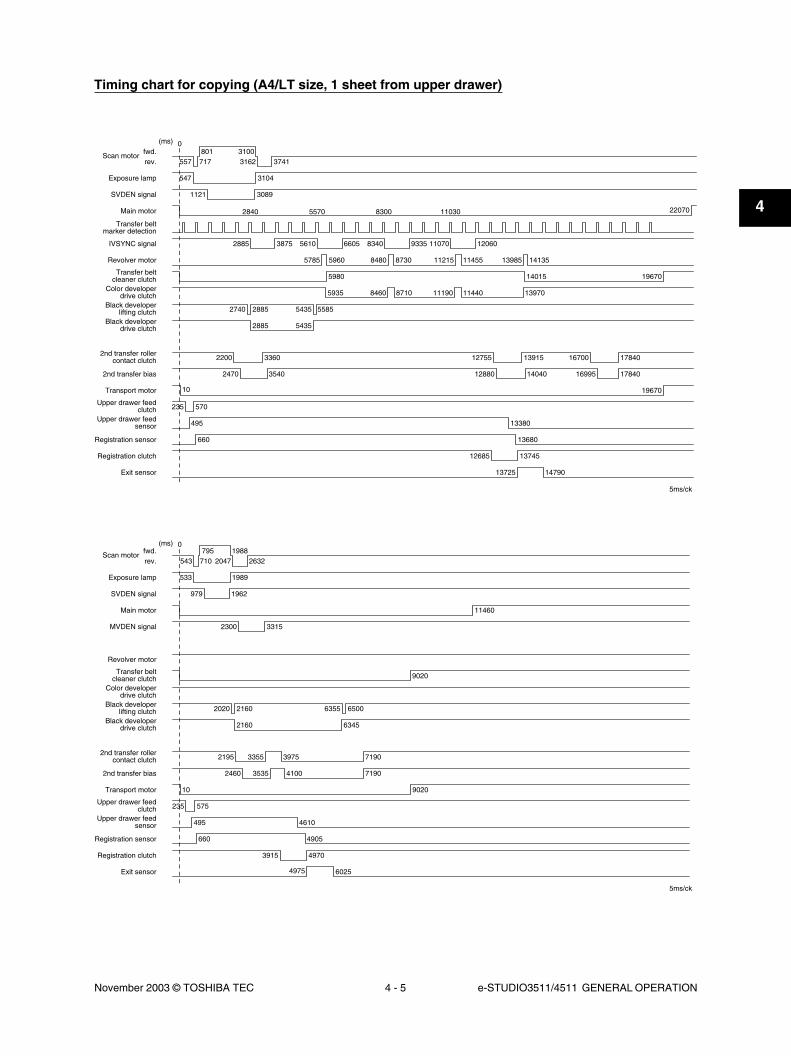
November 2003 © TOSHIBA TEC 4 - 5 e-STUDIO3511/4511 GENERAL OPERATION
4
Timing chart for copying (A4/LT size, 1 sheet from upper drawer)
0
0
10
2885 5610
5785
5570 8300 11030 220702840
8340 110703875
5960 8480 8730 11215 11455 13985 14135
14015
13970114401119087105935
55852885
2885
2740
33602200
35402470
235 570
495
660
1391512755 1784016700
178401699514040
13380
13680
13745
14790
12685
13725
12880
19670
5435
5435
8460
5980 19670
6605 9335 12060
Main motor
1121
31003162
547
557
3089
3104
3741717801
SVDEN signal
Exposure lamp
Scan motorfwd.rev.
Transfer beltmarker detection
Transfer beltcleaner clutch
Color developerdrive clutch
Black developerdrive clutch
Black developerlifting clutch
2nd transfer rollercontact clutch
Upper drawer feedclutch
Upper drawer feedsensor
IVSYNC signal
Revolver motor
Registration sensor
2nd transfer bias
Transport motor
Registration clutch
Exit sensor
(ms)
Main motor
SVDEN signal
Exposure lamp
Scan motorfwd.rev.
Transfer beltcleaner clutch
Color developerdrive clutch
Black developerdrive clutch
Black developerlifting clutch
2nd transfer rollercontact clutch
Upper drawer feedclutch
Upper drawer feedsensor
Revolver motor
Registration sensor
2nd transfer bias
Transport motor
Registration clutch
Exit sensor
(ms)
5ms/ck
5ms/ck
2300
2020
2195
2460
235
3915
4975
3355
3535 4100
575
495 4610
4905
4970
6025
660
10
7190
9020
7190
6355
11460
9020
3315
543
533
979
2047710 2632795 1988
1989
1962
2160
2160
3975
6500
6345
MVDEN signal

e-STUDIO3511/4511 GENERAL OPERATION 4 - 6 November 2003 © TOSHIBA TEC
4
4.2.4 Bypass feed copying(1) Insert a paper into the bypass tray.
• Bypass paper sensor is turned ON.
- “Ready for bypass feeding” is displayed.
• Carriages move to the home position.
(2) Press the [START] button ON
• “Ready for bypass feeding” changes to “COPYING”.
• Exposure lamp ON
• Scan motor ON → Carriages-1 and -2 move forward.
• Main motor, transport motor, developer motor and exit motor turned ON
- The drum, fuser unit, developer unit and exit roller are driven.
• Drum cleaner brush motor turned ON.
(3) Bypass feeding
• Fans rotate in high speed.
• Bypass feed clutch turned ON.
- The bypass pickup roller is lowered.
- The bypass pickup roller, feed roller and separation roller start to rotate.
• Aligning operation
• Paper reaches the registration roller.
• After a certain period of time, the bypass feed clutch turned OFF.
(4) Hereafter, operations (3) through (6) of “4.2.3. Drawer feed copying” are repeated.
4.2.5 Interruption copying(1) Press the [INTERRUPT] button
• LED “INTERRUPT” is turned ON.
• Copying operation in progress is temporarily stopped, and the carriages-1 and -2 return to
appropriate positions.
• “Job interrupted job 1 saved” is displayed.
• Automatic density and reproduction ratio 100% are set. Set number remains the same.
(2) Select the desired copy condition
(3) After interruption copying is finished:
• “Press interrupt to resume job 1” is displayed.
• LED “INTERRUPT” is turned OFF by pressing the [INTERRUPT] button, and the equipment
returns to the status before the interruption.
• “Ready to resume job 1” is displayed.
(4) Press the [START] button
The copying operation before the interruption is resumed.

November 2003 © TOSHIBA TEC 4 - 7 e-STUDIO3511/4511 GENERAL OPERATION
4
4.3 Detection of AbnormalityWhen something abnormal has occurred in the equipment, symbols corresponding to the type of
abnormality are displayed.
4.3.1 Types of abnormalityA) Abnormality cleared without turning OFF the door switch
(1) Add paper
(2) Paper misfeed in bypass
B) Abnormality not cleared without turning OFF the door switch
(1) Misfeed in equipment
(2) Add toner
(3) Developer unit not installed properly
(4) Toner bag replacement
C) Abnormality not cleared without turning OFF the main switch
(1) Call for service
4.3.2 Description of abnormalityA-1) Add paper
[In case of the equipment drawer or PFP drawer] (When drawer is not installed)
Drawer not detected
Drawer is not installed:
Drawer is installed but
there is no paper in it:
→ No paper
↓A signal sent to the control circuit
↓Drawer area of the illustration blinks
(When the drawer is selected)
↓[START] button is disabled.
[In case of the equipment, PFP or LCF drawers] (When drawer is installed)
Based on the combination of the tray-up motor movement and the status of tray-up sensor and
empty sensor, CPU detects the presence of paper.

e-STUDIO3511/4511 GENERAL OPERATION 4 - 8 November 2003 © TOSHIBA TEC
4
• When the power is turned ON or LCF drawer is inserted (When the power is turned ON or equip-
ment/PFP drawers are inserted).
LCF performs initialization.
↓Detects the presence of paper
Tray-up motor ON - The tray goes up
At this time, the tray-up sensor and LCF empty sensor are OFF.
→ When the tray-up sensor is not turned ON in a fixed period of time it means that the tray
is in abnormal condition
“Add paper” is displayed regardless of presence/absence of paper
↓
Cleared by turning the power ON/OFF
→ Tray-up sensor is turned ON in a fixed period of time.
- The tray motor stops.
At this time, if the empty sensor is ON - It is judged that there is paper.
OFF - It is judged that there is no paper.
↓Drawer area of the illustration blinks.
(When the drawer is selected)
• When the paper in the drawer gets short during copying,
→ The tray-up sensor turned OFF
→ The tray-up motor turned ON - Tray goes up
→ Tray-up sensor turned ON
→ Tray-up motor stopped
• Empty sensor turned OFF during the copying in spite of the tray-up sensor is ON
It is judged that there is no paper.
↓Drawer area of the illustration blinks.
(When the drawer is selected)
↓The copying operation is stopped.

November 2003 © TOSHIBA TEC 4 - 9 e-STUDIO3511/4511 GENERAL OPERATION
4
ON
0
Registration clutch
Exit sensor
Timer
ON
Approx 1.2 sec.
Paper jam (E010)
Fig. 4-301
↓
A-2) Bypass misfeeding ( )
• During bypass feeding
Bypass feed clutch is turned ON
↓Registration sensor is turned ON
* Registration sensor is not turned ON in a fixed period of time (E120)
↓Bypass misfeeding
↓Bypass misfeed symbol is displayed ( )
↓The copying operation is disabled.
↓Solution: The bypass sensor is turned OFF by removing the paper from the bypass tray.
A-3) Set key copy counter
• When the key copy counter (optional) is pulled out from the equipment which installs it: “Set key
copy counter” displayed.
↓Copying operation disabled
• When the counter is pulled out during copying:
Copying is stopped when the key copy counter is pulled out.
B-1) Misfeed in equipment ( )
• Exit sensor detects jamming of the leading edge
of paper
Registration clutch turned ON
↓ Approx 1.2 sec.*
Exit sensor turned ON
If the exit sensor is not turned ON after
approx 1.2 seconds,
↓Paper jam (E010) → The copying operation is
stopped.

e-STUDIO3511/4511 GENERAL OPERATION 4 - 10 November 2003 © TOSHIBA TEC
4
• Exit sensor detects jamming of the trailing edge of
paper
Registration clutch turned OFF
↓ Approx 1.3 sec*
Exit sensor turned OFF
If the exit sensor is not turned OFF
after approx 1.3 seconds,
↓Paper jam (E020) → The copying operation is
stopped.
• Immediately after the power ON
↓Any of all sensors on paper transport path detects paper (ON)
↓Paper jam (E030)
• Front cover is opened during copying
↓Paper jam (E410)
• Registration sensor detects jamming of the leading edge of paper:
The registration sensor is not turned ON in a fixed period of time after the leading edge of paper
passed the transport roller.
↓Paper jam (E120, E200, E210, E300, E330 and E3C0)
• During paper feeding from ADU:
The registration sensor is not turned ON in a fixed period of time after the ADU clutch is turned
ON.
↓Paper jam (E110)
• During paper transporting from ADU:
ADU entrance/exit sensors do not detect the paper at the fixed timing
↓Paper jam (E510 and E520)
• During paper feeding from the equipment or PFP:
The registration sensor is not turned ON in a fixed period of time after the feed clutch is turned
ON.
↓Paper jam (E220, E310, E320, E340 to E360, E3D0 and E3E0: Error code defers depending on
the paper source.)
Registration clutch
Exit sensor
Timer
ON
OFF
Approx 1.3 sec.
Paper jam (E020)
Fig. 4-302

November 2003 © TOSHIBA TEC 4 - 11 e-STUDIO3511/4511 GENERAL OPERATION
4
B-2) Add toner ( )
Toner density becomes low
↓Auto-toner sensor detects the absence of the toner
↓Control circuit → “Add toner” is displayed: the copying operation disabled
Solution: Open the front cover and replace the toner cartridge with new one.
Toner is supplied → copying operation enabled
B-3) Developer unit not installed properly
Disconnection of the connectors of the developer unit
↓“Developer unit not installed” is displayed.
Solution: Connect the connectors of the developer unit and close the front cover.
B-4) Toner bag replacement ( )
• Toner bag is full of used toner
↓Toner recovery auger shifts to the rear side: Toner bag full detection sensor-1 ON
↓“Dispose of used toner” is displayed
• Toner bag full detection sensor is turned ON during printing
↓Printing is stopped after the paper being printed is exited
Solution: Replace the toner bag with new one and close the front cover.
C-1) Call for service
Error code is displayed instead of the set number by pressing the [CLEAR] button and [8] button
simultaneously when the “Call for service” is blinking.
Refer to the error code table in the Service Handbook.

e-STUDIO3511/4511 GENERAL OPERATION 4 - 12 November 2003 © TOSHIBA TEC
4
4.4 Flow Chart4.4.1 Power ON to ready
YES
A
B
NO
NO
Registration sensorON?
Exit sensorON?
ADUentrance/exit sensor
ON?
Main switch ON
DC power ON
Cover open?YES
NO
IH coil ONFans ON
Paper jam
Restart
"E030"
NO
NO
NO
NO
YES
YES
Call for service
YES
YES
"C260"
YES
Call for service
"CF50"
NO
Call for service
"CEA0"
NO
Call for service
"CE10""CE20""CE40""CE50""CE90"
Upper drawerfeed sensor ON?
Lower drawerfeed sensor ON?
NO
NO
NO
NO
YES
YES
YES
YES
"C270""C280"
Scan motor ON
Home positiondetected?
Peak detected?
Main motor ONRevolver motor ONPolygonal motor ON
Colortoner sensorabnormal?
Revolverhome position
detected?
Imagequality control finished
propery?
YES
YES
Revolverinitialization
finished?
2.5 sec. Elapsed?
Call for service
Performs image quality control

November 2003 © TOSHIBA TEC 4 - 13 e-STUDIO3511/4511 GENERAL OPERATION
4
A
B
Fuser beltreached ready
temp.?
YES
YES "C410""C430"Call for service
"C440"Call for service
"CA10"Call for service
"C470""C480""C490"
Call for service
READY
Fuserbelt ready for pre-
running?
Transport motor ONTray-up motor ON
Main motor OFFRevolver motor OFFTransport motor OFFTray-up motor OFF
IH coil OFF
NO
Thermistor broken?
NO
NO
YES
IH coil broken?
NO
YES
Polygonalmotor condition
abnormal?
NO
YES
IH error?
NO
YES

e-STUDIO3511/4511 GENERAL OPERATION 4 - 14 November 2003 © TOSHIBA TEC
4
4.4.2 Automatic feed copying
Press [START]
READY
Transport system control Scanner system control
Scanner systemcontrol completed
Feed clutch ON
Exposure lamp ON
Remainingset number=0?
Transport motor ONExit motor ON
Registration clutch ONCounter ON/OFF
Main motor OFFTransport motor OFFDeveloper motor OFF
Exit motor OFF
NG
Paper jam
"E020"
NG
Paper jam
"E010"
Feed clutch OFF
Registration clutch OFF
Exit sensorcheck leading
edge?
YES
Exit sensorcheck trailing
edge?
NO
NO
YES
Call for service
"CA10"
Polygonalmotor normal
rotation?
NO
YES
YES
Color printed?
OK
Carriage stopped
Carriage stopped
Exposure lamp OFF
Carriage moves backward
Carriage moves forward
Processing system control
Main motor ONDeveloper motor ON
Drum cleaner brush motor ON
C
F
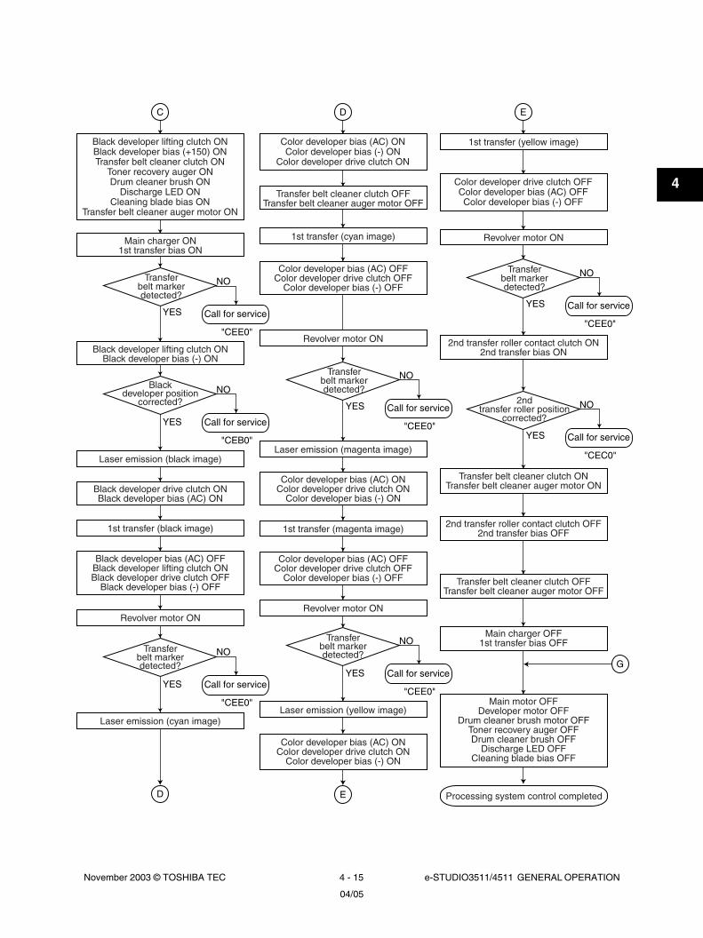
November 2003 © TOSHIBA TEC 4 - 15 e-STUDIO3511/4511 GENERAL OPERATION
4
Main charger ON1st transfer bias ON
Black developer bias (AC) OFFBlack developer lifting clutch ONBlack developer drive clutch OFF
Black developer bias (-) OFF
Transferbelt markerdetected?
Black developer lifting clutch ONBlack developer bias (+150) ONTransfer belt cleaner clutch ON
Toner recovery auger ONDrum cleaner brush ON
Discharge LED ONCleaning blade bias ON
Transfer belt cleaner auger motor ON
NO
YES Call for service
"CEE0"
Black developer lifting clutch ONBlack developer bias (-) ON
Black developer drive clutch ONBlack developer bias (AC) ON
YES
Laser emission (black image)
1st transfer (black image)
Revolver motor ON
Laser emission (cyan image)
Blackdeveloper position
corrected?NO
Call for service
"CEB0"
YES
Transferbelt markerdetected?
NO
Call for service
"CEE0"
C
D
G
Transfer belt cleaner clutch OFFTransfer belt cleaner auger motor OFF
Transferbelt markerdetected?
Color developer bias (AC) ONColor developer bias (-) ON
Color developer drive clutch ON
NO
YES Call for service
"CEE0"
Color developer bias (AC) ONColor developer drive clutch ON
Color developer bias (-) ON
Laser emission (magenta image)
Color developer bias (AC) OFFColor developer drive clutch OFF
Color developer bias (-) OFF
1st transfer (magenta image)
Color developer bias (AC) OFFColor developer drive clutch OFF
Color developer bias (-) OFF
1st transfer (cyan image)
Revolver motor ON
Revolver motor ON
Laser emission (yellow image)
Color developer bias (AC) ONColor developer drive clutch ON
Color developer bias (-) ON
YES
Transferbelt markerdetected?
NO
Call for service
"CEE0"
D
E
Transferbelt markerdetected?
Color developer drive clutch OFFColor developer bias (AC) OFFColor developer bias (-) OFF
NO
YES Call for service
"CEE0"
2ndtransfer roller position
corrected?NO
YES Call for service
"CEC0"
2nd transfer roller contact clutch ON2nd transfer bias ON
2nd transfer roller contact clutch OFF2nd transfer bias OFF
Transfer belt cleaner clutch ONTransfer belt cleaner auger motor ON
Transfer belt cleaner clutch OFFTransfer belt cleaner auger motor OFF
Main charger OFF1st transfer bias OFF
Main motor OFFDeveloper motor OFF
Drum cleaner brush motor OFFToner recovery auger OFFDrum cleaner brush OFF
Discharge LED OFFCleaning blade bias OFF
1st transfer (yellow image)
Revolver motor ON
E
Processing system control completed
04/05

e-STUDIO3511/4511 GENERAL OPERATION 4 - 16 November 2003 © TOSHIBA TEC
4
Main charger ON1st transfer bias ON
Black developer lifting clutch ONBlack developer bias (-) ON
2nd transfer roller contact clutch ON2nd transfer bias ON
2nd transfer roller contact clutch OFF2nd transfer bias OFF
Transfer belt cleaner clutch OFFTransfer belt cleaner auger motor OFF
1st transfer bias OFF
Black developer bias (AC) OFFBlack developer lifting clutch ONBlack developer drive clutch OFF
Black developer bias (-) OFFMain charger OFF
Blackdeveloper position
corrected?
Black developer lifting clutch ONBlack developer bias (+150) ONTransfer belt cleaner clutch ON
Toner recovery auger ONDrum cleaner brush ON
Discharge LED ONCleaning blade bias ON
Transfer belt cleaner auger motor ON
NO
YES Call for service
"CEB0"
Black developer drive clutch ONBlack developer bias (AC) ON
Laser emission (black image)
1st transfer (black image)
YES
2ndtransfer roller position
corrected?NO
Call for service
"CEC0"
F
G
04/05

November 2003 © TOSHIBA TEC 5 - 1 e-STUDIO3511/4511 CONTROL PANEL
5
5. CONTROL PANEL
5.1 Control Panel and Display PanelThe control panel consists of button switches and touch-panel switches to operate equipment and select
various modes, and LEDs and an LCD to display the state of the equipment or the messages.
When the operator’s attention is required, graphic symbols appear with messages explaining the condition
of the equipment in the LCD panel.
This equipment has a movable control panel which enables to adjust its angle to the operator. It also has
improved its operatability and visibility with the enlarged LCD panel.
[Control Panel Outside View]
Fig. 5-101

e-STUDIO3511/4511 CONTROL PANEL 5 - 2 November 2003 © TOSHIBA TEC
5
5.2 Items Shown on the Display Panel
Fig. 5-201
Fig. 5-202
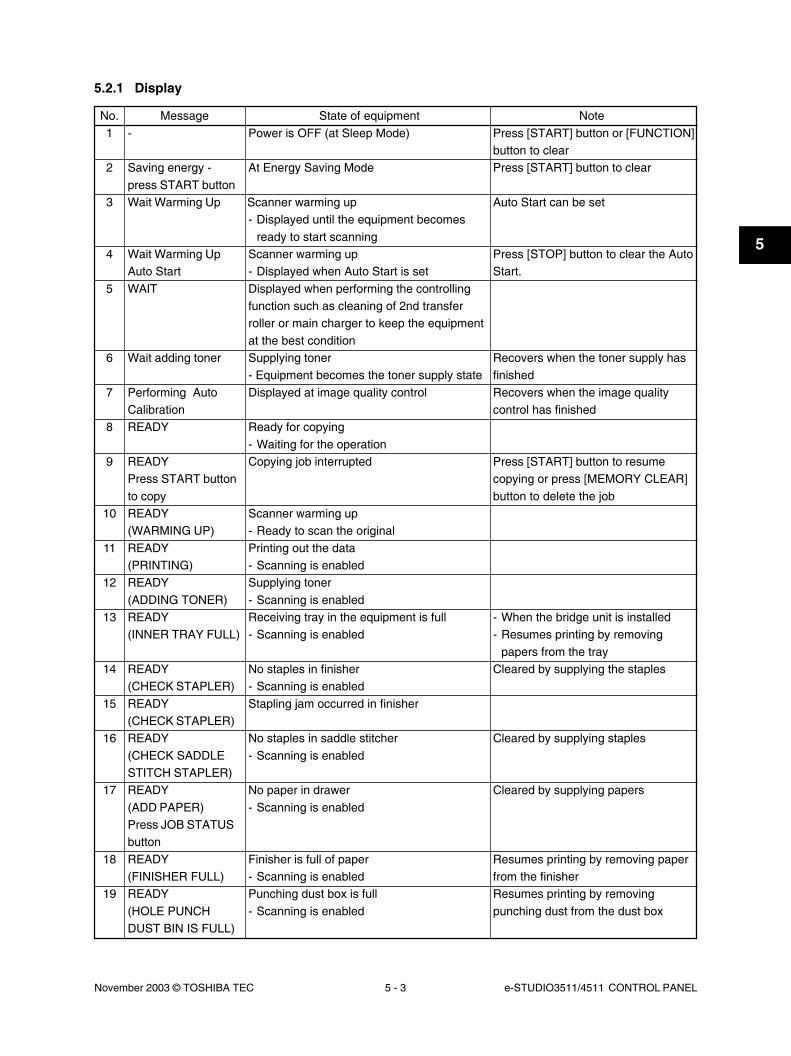
November 2003 © TOSHIBA TEC 5 - 3 e-STUDIO3511/4511 CONTROL PANEL
5
Power is OFF (at Sleep Mode)
At Energy Saving Mode
Scanner warming up- Displayed until the equipment becomes
ready to start scanningScanner warming up- Displayed when Auto Start is setDisplayed when performing the controllingfunction such as cleaning of 2nd transferroller or main charger to keep the equipmentat the best conditionSupplying toner- Equipment becomes the toner supply stateDisplayed at image quality control
Ready for copying- Waiting for the operationCopying job interrupted
Scanner warming up- Ready to scan the originalPrinting out the data- Scanning is enabledSupplying toner- Scanning is enabledReceiving tray in the equipment is full- Scanning is enabled
No staples in finisher- Scanning is enabledStapling jam occurred in finisher
No staples in saddle stitcher- Scanning is enabled
No paper in drawer- Scanning is enabled
Finisher is full of paper- Scanning is enabledPunching dust box is full- Scanning is enabled
Press [START] button or [FUNCTION]button to clearPress [START] button to clear
Auto Start can be set
Press [STOP] button to clear the AutoStart.
Recovers when the toner supply hasfinishedRecovers when the image qualitycontrol has finished
Press [START] button to resumecopying or press [MEMORY CLEAR]button to delete the job
- When the bridge unit is installed- Resumes printing by removing
papers from the trayCleared by supplying the staples
Cleared by supplying staples
Cleared by supplying papers
Resumes printing by removing paperfrom the finisherResumes printing by removingpunching dust from the dust box
-
Saving energy -press START buttonWait Warming Up
Wait Warming UpAuto StartWAIT
Wait adding toner
Performing AutoCalibrationREADY
READYPress START buttonto copyREADY(WARMING UP)READY(PRINTING)READY(ADDING TONER)READY(INNER TRAY FULL)
READY(CHECK STAPLER)READY(CHECK STAPLER)READY(CHECK SADDLESTITCH STAPLER)READY(ADD PAPER)Press JOB STATUSbuttonREADY(FINISHER FULL)READY(HOLE PUNCHDUST BIN IS FULL)
1
2
3
4
5
6
7
8
9
10
11
12
13
14
15
16
17
18
19
5.2.1 Display
No. Message State of equipment Note

e-STUDIO3511/4511 CONTROL PANEL 5 - 4 November 2003 © TOSHIBA TEC
5
No. Message State of equipment Note20
21
22
23
24
25
26
27
28
29
30
31
32
33
34
35
36
37
38
39
READY(SADDLE STITCHTRAY FULL)READY(CHANGE DRAWERTO CORRECTPAPER SIZE)Ready for bypassfeedingCOPYING
Auto Start
Close Large CapacityFeederClose Large CapacityFeeder DoorPlace Doc. Feeder inthe down positionInsert key copycounterPlace originals in thedocument feeder
Change direction oforiginalPlace last %doriginals in doc.feeder entrance trayCannot copy thisoriginalAdd paper
Cannot duplex thissizeCannot use thismedia type
Copy size: A4/LTonly
Copy size: A4/LT andA4-R/LT-RCHANGE DRAWERTO CORRECTPAPER SIZEChange drawer tocorrect media type
Saddle stitcher tray is full of paper- Scanning is enabled
Incorrect paper size setting
Paper is set on the bypass tray
At the copying state
Auto Start is set during printing
LCF drawer is not installed when feedingfrom LCF is setLCF cover is open when feeding from LCF issetRADF is open when original is placed onRADFKey copy counter not inserted
Displayed when the conditions are set andSTART button is pressed with no originalplacedDisplayed when the direction of originalplaced is different from the settingPaper jam occurred during copying (RADFscanning)
Displayed when the original which is notallowed to be copied is placedDisplayed when the paper in selected draweris running outDisplayed when the paper size which is notspecified for duplex copying is setDisplayed when the paper size which is notspecified for the functions such as stapling orhole punching is setDisplayed when the paper size which is notspecified for “Book-type duplex copying” or“Dual-page” is setDisplayed when the paper size which is notspecified for “Rotate Sort”Displayed when the selected paper size isnot in the drawer
Displayed when the selected media type isnot in the drawer
Cleared by pressing [RESET] buttonor [STOP] buttonCleared by installing LCF drawer
Cleared by closing the cover
Cleared by closing RADF
Cleared by inserting key copycounterCleared by setting the original
Not printed out
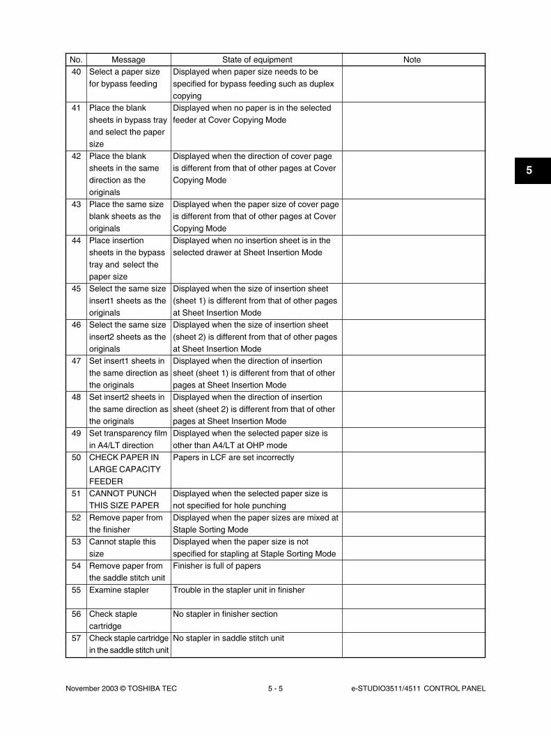
November 2003 © TOSHIBA TEC 5 - 5 e-STUDIO3511/4511 CONTROL PANEL
5
Displayed when paper size needs to bespecified for bypass feeding such as duplexcopyingDisplayed when no paper is in the selectedfeeder at Cover Copying Mode
Displayed when the direction of cover pageis different from that of other pages at CoverCopying Mode
Displayed when the paper size of cover pageis different from that of other pages at CoverCopying ModeDisplayed when no insertion sheet is in theselected drawer at Sheet Insertion Mode
Displayed when the size of insertion sheet(sheet 1) is different from that of other pagesat Sheet Insertion ModeDisplayed when the size of insertion sheet(sheet 2) is different from that of other pagesat Sheet Insertion ModeDisplayed when the direction of insertionsheet (sheet 1) is different from that of otherpages at Sheet Insertion ModeDisplayed when the direction of insertionsheet (sheet 2) is different from that of otherpages at Sheet Insertion ModeDisplayed when the selected paper size isother than A4/LT at OHP modePapers in LCF are set incorrectly
Displayed when the selected paper size isnot specified for hole punchingDisplayed when the paper sizes are mixed atStaple Sorting ModeDisplayed when the paper size is notspecified for stapling at Staple Sorting ModeFinisher is full of papers
Trouble in the stapler unit in finisher
No stapler in finisher section
No stapler in saddle stitch unit
Select a paper sizefor bypass feeding
Place the blanksheets in bypass trayand select the papersizePlace the blanksheets in the samedirection as theoriginalsPlace the same sizeblank sheets as theoriginalsPlace insertionsheets in the bypasstray and select thepaper sizeSelect the same sizeinsert1 sheets as theoriginalsSelect the same sizeinsert2 sheets as theoriginalsSet insert1 sheets inthe same direction asthe originalsSet insert2 sheets inthe same direction asthe originalsSet transparency filmin A4/LT directionCHECK PAPER INLARGE CAPACITYFEEDERCANNOT PUNCHTHIS SIZE PAPERRemove paper fromthe finisherCannot staple thissizeRemove paper fromthe saddle stitch unitExamine stapler
Check staplecartridgeCheck staple cartridgein the saddle stitch unit
No. Message State of equipment Note40
41
42
43
44
45
46
47
48
49
50
51
52
53
54
55
56
57

e-STUDIO3511/4511 CONTROL PANEL 5 - 6 November 2003 © TOSHIBA TEC
5
Interrupt copying is accepted
Interrupt copying is cancelled (finished)
Displayed when reproduction ratio is set tobe over 200% at AMS Mode on RADFDisplayed when reproduction ratio is setmanually to be over 200% on RADFDisplayed when the template stored isrecalled by pressing [TEMPLATE] buttonDisplayed when a button is pressed while thedepartment management setting is availableDisplayed when the number of printoutsexceeds the limit number of departmentcounter
Displayed when the number of printoutsexceeds the limit number of departmentcounter
Displayed when the number of printoutsexceeds the limit number of departmentcounter
Displayed when the number of printoutsexceeds the limit number of departmentcounterDisplayed when confirming the user to printout the data as much as stored at memory- full state
Displayed when confirming the user to sendthe FAX data as much as stored at memory- full state
Displayed when confirming the user to savethe scanning data as much as stored atmemory-full state
Displayed when confirming the user to printout the data as much as stored at memory-full state
Displayed when confirming the user to sendthe FAX data as much as stored at memory-full state
Set the reproduction ratio 200% orbelow manuallySet the reproduction ratio 200% orbelow
Displayed only in FAX Function
Displayed only in FAX Function
Displayed only in FAX Function
58
59
60
61
62
63
64
65
66
67
68
69
70
71
72
Job interrupted job 1savedReady to resume job1Cannot use AMSmodeMore than 200% isnot availableUpdated the templatesettingEnter DepartmentCodeCannot copy BLACKmode CheckDEPARTMENTCOUNTERCannot copy FULLCOLOR mode CheckDEPARTMENTCOUNTERCannot copy TWINCOLOR mode CheckDEPARTMENTCOUNTERCannot copy CheckDEPARTMENTCOUNTERNot enough memoryto store original(s)Will you print outstored originals?Not enough memoryto store original(s)Will you send storedoriginals in?Not enough memoryto store original(s)Will you save storedoriginals in?The number oforiginals exceeds thelimits Will you copystored originals?The number oforiginals exceeds thelimits.Will you send storedoriginals?
No. Message State of equipment Note

November 2003 © TOSHIBA TEC 5 - 7 e-STUDIO3511/4511 CONTROL PANEL
5
Displayed when confirming the user to savethe scanning data as much as stored atmemory-full state
No black toner in the cartridge
No yellow toner in the cartridge
No magenta toner in the cartridge
No cyan toner in the cartridge
No yellow and magenta toner in thecartridgesNo yellow and cyan toner in the cartridges
No magenta and cyan toner in the cartridges
Three colors of toner are running out in thecartridgesPM cycle- Displayed at the time for maintenance- Copying is availableDisplays when the printing is stoppedbecause of media type mismatch
Displays the warning that the copy is notenabled when any drawer but bypass feed isselected at Cover Sheet Mode or SheetInsertion Mode.Paper jam in the equipment- Displayed when paper jam occurred in the
equipmentDisplayed when motor, sensor, switch, etc.do not work properlyDisplayed when the Department Code canno be keyed in immediately after power-ON.Displayed when the paper size which is notacceptable is set (depends on the setting)
Displayed only in Scanning Function
Displayed when black toner isrunning out even if other toner stillremain. Copying not enabledBlack copying is availableOther button functions are availableBlack copying is availableOther button functions are availableBlack copying is availableOther button functions are availableBlack copying is availableOther button functions are availableBlack copying is availableOther button functions are availableBlack copying is availableOther button functions are availableBlack copying is availableOther button functions are availableMaintenance and inspection areperformed by qualified servicetechnician.
Remove the paper in the equipmentaccording to the messages displayedon the panel.Turn OFF the power and solve theproblem, then turn ON the power.Leave it for a while and key in thecode againReset the paper size
73
74
75
76
77
78
79
80
81
82
83
84
85
86
87
88
The number oforiginals exceeds thelimits.Will you save storedoriginals?Install new Blacktoner cartridge
Install new Yellowtoner cartridgeInstall new Magentatoner cartridgeInstall new Cyantoner cartridgeInstall new Y and Mtoner cartridgeInstall new Y and Ctoner cartridgeInstall new M and Ctoner cartridgeInstall new colortoner cartridgeTime for periodicmaintenance
READY(CHANGE DRAWERTO CORRECTMEDIA TYPE)PRESS [BASIC]and select normalpaper size
Misfeed in copierPress [HELP]
Call for service
Please try again aftera whileSet standard size
No. Message State of equipment Note

e-STUDIO3511/4511 CONTROL PANEL 5 - 8 November 2003 © TOSHIBA TEC
5
5.3 Relation between the Equipment State and Operator’s Operation
Pre
ss [E
NE
RG
YS
AV
ER
] but
ton
Pre
ss [A
CC
ES
S]
butto
n
Pre
ss [J
OB
ST
AT
US
]bu
tton
Pre
ss [I
NT
ER
RU
PT
]bu
tton
Pre
ss [F
UN
CT
ION
CLE
AR
] but
ton
afte
rse
tting
the
copy
mod
e
Pre
ss [S
TO
P] b
utto
n
Pre
ss [C
LEA
R] b
utto
naf
ter
setti
ng th
e co
pym
ode
Pre
ss [C
LEA
R] b
utto
naf
ter
keyi
ng in
num
bers
(dig
ital k
eys)
Pre
ss [M
ON
ITO
R/
PA
US
E]
Pre
ss [F
AX
] but
ton
Pre
ss [C
OP
Y] b
utto
n
Pre
ss [S
CA
N] b
utto
n
Pre
ss [
e-F
ILIN
G]
Pre
ss [E
XT
EN
SIO
N]
butto
nP
ress
[TE
MP
LAT
E]
butto
nP
ress
[US
ER
FU
NC
TIO
NS
] bu
tton
Pre
ss [H
ELP
] but
ton
Pre
ss [S
TA
RT
] but
ton
with
the
orig
inal
set
on
RA
DF
Dur
ing
RE
AD
Y s
tatu
s
Sw
itche
s to
ene
rgy
savi
ng m
ode
Dis
play
s de
part
men
tco
de e
ntry
scr
een
(whe
n de
part
men
tm
anag
emen
t is
avai
labl
e)D
ispl
ays
prin
t job
list
scre
enS
witc
hes
to in
terr
upt
mod
eC
opy
mod
e is
cle
ared
afte
r th
e co
py m
ode
isse
t
Dis
play
not
cha
nged
Num
ber
of p
rinto
uts
chan
ges
to 1
whi
leth
e se
tting
rem
ains
unch
ange
d af
ter
the
copy
mod
e is
set
Num
ber
keye
d in
chan
ges
to 1
afte
rbe
ing
ente
red
Dis
play
not
cha
nged
Dis
play
s F
AX
scr
een
Dis
play
not
cha
nged
Dis
play
s S
CA
Nsc
reen
Dis
play
s e-
FIL
ING
scre
enD
ispl
ay n
ot c
hang
ed
Dis
play
s T
EM
PLA
TE
scre
enD
ispl
ays
US
ER
FU
NC
TIO
NS
scr
een
Dis
play
s H
ELP
scre
en
Dis
play
s “C
OP
YIN
G”
Dur
ing
war
min
g-up
Dis
play
not
cha
nged
Dis
play
s de
part
men
tco
de e
ntry
scr
een
(whe
n de
part
men
tm
anag
emen
t is
avai
labl
e)D
ispl
ay n
ot c
hang
ed
Dis
play
not
cha
nged
Cop
y m
ode
is c
lear
edaf
ter
the
copy
mod
e is
set
Dis
play
not
cha
nged
Num
ber
of p
rinto
uts
chan
ges
to 1
whi
leth
e se
tting
rem
ains
unch
ange
d af
ter
the
copy
mod
e is
set
Num
ber
keye
d in
chan
ges
to 1
afte
rbe
ing
ente
red
Dis
play
not
cha
nged
Dis
play
not
cha
nged
Dis
play
not
cha
nged
Dis
play
not
cha
nged
Dis
play
not
cha
nged
Dis
play
not
cha
nged
Dis
play
not
cha
nged
Dis
play
not
cha
nged
Dis
play
s H
ELP
scre
en
“Wai
t War
min
g U
pA
uto
Sta
rt”
isdi
spla
yed
Aut
o jo
b st
art
rese
rved
Dis
play
not
cha
nged
Dis
play
not
cha
nged
Dis
play
not
cha
nged
Dis
play
not
cha
nged
Aut
o jo
b st
art
canc
elle
d
Aut
o jo
b st
art
canc
elle
d
Dis
play
not
cha
nged
Dis
play
not
cha
nged
Dis
play
not
cha
nged
Dis
play
not
cha
nged
Dis
play
not
cha
nged
Dis
play
not
cha
nged
Dis
play
not
cha
nged
Dis
play
not
cha
nged
Dis
play
not
cha
nged
Dis
play
not
cha
nged
Dis
play
not
cha
nged
Dis
play
not
cha
nged
Sca
nnin
g or
igin
al/
Sca
nnin
g or
igin
al a
ndpr
intin
g ou
t the
cop
yD
ispl
ay n
ot c
hang
ed
Dis
play
not
cha
nged
Dis
play
s pr
int j
ob li
stsc
reen
Dis
play
not
cha
nged
(LE
D b
linki
ng)
Dis
play
not
cha
nged
Sca
nnin
g or
prin
ting
out s
tops
, and
“RE
AD
Y P
ress
ST
AR
T to
cop
y“ a
nd“M
EM
OR
Y C
LEA
R”
are
disp
laye
dD
ispl
ay n
ot c
hang
ed
Dis
play
not
cha
nged
Dis
play
not
cha
nged
Dis
play
not
cha
nged
Dis
play
not
cha
nged
Dis
play
not
cha
nged
Dis
play
not
cha
nged
Dis
play
not
cha
nged
Dis
play
not
cha
nged
Dis
play
not
cha
nged
Dis
play
not
cha
nged
Dis
play
not
cha
nged
Prin
ting
out t
he c
opy
Dis
play
not
cha
nged
Dis
play
s de
part
men
tco
de e
ntry
scr
een
(whe
n de
part
men
tm
anag
emen
t is
avai
labl
e)D
ispl
ays
prin
t job
list
scre
enD
ispl
ay n
ot c
hang
ed(L
ED
blin
king
)C
opy
mod
e is
cle
ared
afte
r th
e co
py m
ode
is s
et
Prin
ting
out s
tops
,an
d “R
EA
DY
Pre
ssS
TA
RT
to c
opy“
and
“ME
MO
RY
CLE
AR
”ar
e di
spla
yed
Num
ber
of p
rinto
uts
chan
ges
to 1
whi
leth
e se
tting
rem
ains
unch
ange
d af
ter
the
copy
mod
e is
set
Num
ber
keye
d in
chan
ges
to 1
afte
rbe
ing
ente
red
Dis
play
not
cha
nged
Dis
play
s F
AX
scr
een
Dis
play
not
cha
nged
Dis
play
s S
CA
Nsc
reen
Dis
play
s e-
FIL
ING
scre
enD
ispl
ay n
ot c
hang
ed
Dis
play
s T
EM
PLA
TE
scre
enD
ispl
ays
US
ER
FU
NC
TIO
NS
scr
een
Dis
play
s H
ELP
scre
en
Dis
play
s “C
OP
YIN
G”
and
RA
DF
sta
rts
feed
ing
Dur
ing
pape
r ja
m
Dis
play
not
cha
nged
Dis
play
not
cha
nged
Dis
play
not
cha
nged
Dis
play
not
cha
nged
Dis
play
not
cha
nged
Dis
play
not
cha
nged
Dis
play
not
cha
nged
Dis
play
not
cha
nged
Dis
play
not
cha
nged
Dis
play
not
cha
nged
Dis
play
not
cha
nged
Dis
play
not
cha
nged
Dis
play
not
cha
nged
Dis
play
not
cha
nged
Dis
play
not
cha
nged
Dis
play
not
cha
nged
Dis
play
not
cha
nged
Dis
play
not
cha
nged
Whe
n in
terr
uptin
g
Dis
play
not
cha
nged
Dis
play
s de
part
men
tco
de e
ntry
scr
een
(whe
n de
part
men
tm
anag
emen
t is
avai
labl
e)D
ispl
ays
prin
t job
list
scre
enR
etur
ns to
the
stat
usbe
fore
inte
rrup
ting
Cop
y m
ode
is c
lear
edaf
ter
the
copy
mod
eis
set
Dis
play
not
cha
nged
Num
ber
of p
rinto
uts
chan
ges
to 1
whi
leth
e se
tting
rem
ains
unch
ange
d af
ter
the
copy
mod
e is
set
Num
ber
keye
d in
chan
ges
to 1
afte
rbe
ing
ente
red
Dis
play
not
cha
nged
Dis
play
not
cha
nged
Dis
play
not
cha
nged
Dis
play
not
cha
nged
Dis
play
not
cha
nged
Dis
play
not
cha
nged
Dis
play
not
cha
nged
Dis
play
not
cha
nged
Dis
play
s H
ELP
scre
en
Dis
play
s “C
OP
YIN
G”
and
RA
DF
sta
rts
feed
ing
Whe
n di
spla
ying
HE
LP s
cree
n
Sw
itche
s to
ene
rgy
savi
ng m
ode
Dis
play
s de
part
men
tco
de e
ntry
scr
een
(whe
n de
part
men
tm
anag
emen
t is
avai
labl
e)D
ispl
ays
prin
t job
list
scre
enS
witc
hes
toin
terr
uptin
g m
ode
Dis
play
s B
AS
ICsc
reen
afte
r th
e co
pym
ode
is s
et a
nd th
enca
ncel
led
Dis
play
not
cha
nged
Num
ber
of p
rinto
uts
chan
ges
to 1
whi
leth
e se
tting
rem
ains
unch
ange
d af
ter
the
copy
mod
e is
set
Num
ber
keye
d in
chan
ges
to 1
afte
rbe
ing
ente
red
Dis
play
not
cha
nged
Dis
play
s F
AX
scr
een
Dis
play
not
cha
nged
Dis
play
s S
CA
Nsc
reen
Dis
play
s e-
FIL
ING
scre
enD
ispl
ay n
ot c
hang
ed
Dis
play
s T
EM
PLA
TE
scre
enD
ispl
ays
US
ER
FU
NC
TIO
NS
scr
een
Sw
itche
s to
the
scre
en p
revi
ousl
ydi
spla
yed
Dis
play
s “C
OP
YIN
G”
and
RA
DF
sta
rts
feed
ing
Dur
ing
ener
gy s
avin
gm
ode
Ene
rgy
savi
ng m
ode
is c
lear
ed a
nddi
spla
ys B
AS
ICsc
reen
Dis
play
not
cha
nged
Dis
play
not
cha
nged
Dis
play
not
cha
nged
Dis
play
not
cha
nged
Dis
play
not
cha
nged
Dis
play
not
cha
nged
Dis
play
not
cha
nged
Dis
play
not
cha
nged
Dis
play
s F
AX
scr
een
Dis
play
s C
OP
Ysc
reen
Dis
play
s S
CA
Nsc
reen
Dis
play
s e-
FIL
ING
scre
enD
ispl
ay n
ot c
hang
ed
Dis
play
not
cha
nged
Dis
play
not
cha
nged
Dis
play
not
cha
nged
Ene
rgy
savi
ng m
ode
iscl
eare
d an
d di
spla
ysB
AS
IC s
cree
n

November 2003 © TOSHIBA TEC 5 - 9 e-STUDIO3511/4511 CONTROL PANEL
5
5.4 Description of Operation5.4.1 Dot matrix LCD circuit
(1) Structure
The DSP-LCD-350 is an STN blue mode transmissive type LCD with 640x240-dot display capacity. It
consists of a driver LSI, frame, printed circuit board, and lateral type CCFL backlight.
* STN: Super Twisted Nematic
* CCFL:Cold Cathod Fluorescent Lamp
(2) Block diagram
(640 x 240)
IC1
XSCL
UD0UD1UD2UD3
WF
LP
VDDGNDV0VEE
Power supply
LCDEN
IC2
LCD PANEL640 x 240 DOTS
IC3 IC4
160 160 160 160
IC5 120
IC6 120
Fig. 5-401
Fig. 5-402

e-STUDIO3511/4511 CONTROL PANEL 5 - 10 November 2003 © TOSHIBA TEC
5
(4) Data Transmission
(3) System diagram
Signals flowing between the control panel and the system board are indicated in the chart below.
When the panel processing CPU detects that the control panel is operated, the operational contents are
transmitted to the System board through the serial data. The state of the equipment and the messages
from the System board are received by the LCD controller and then displayed on the LCD. The LED and
buzzers are switched to ON/OFF with the signals from the System control PC board.
LOAD
FRAME
LOAD
240 1 2 240
CP x(640/4) pulses
1 2 240
1/tF1/tF
1 2
FRAME
D0-D3
CP
Fig. 5-403
Fig. 5-404
Inverter forbacklight
Contrast adjustmentcircuit
LCD display640 x 240 dots
LCDcontroller
Analoginput
LED driver
Buzzer
Touch panel
Decoder
Hard-key matrix
LEDBuzzer ON signal
LED serial output
Serial data
Power ON/OFFReset signals
LED scan signal
Panelprocessing
CPU
System control PC board Control panel

November 2003 © TOSHIBA TEC 5 - 11 e-STUDIO3511/4511 CONTROL PANEL
5
LDON0"L"
"L" 17D7
Q3
IC
R3(COPY)
5VL
LED
G
5.4.2 LED display circuit
(1) Method of LED display
ex) Displaying “COPY” .
Transistor is turned ON when the LDON 0 signal becomes “L” level.
Also, when IC pin changes to “L”, the current flows from 5VL via the transistor to the LED (“COPY”)
to turn ON the LED (“COPY”).
Current
Conditions to turn ON the LED
(a) The transistor (Q3) connected to the LED anode is ON.
(b) The output from the cathode side of the LED is “L” level.
The LED turns ON when the conditions (a) and (b) are met.
Fig. 5-405

e-STUDIO3511/4511 CONTROL PANEL 5 - 12 November 2003 © TOSHIBA TEC
5
5.5 Disassembly and ReplacementNote: When taking off the control panel, check the
position of the stopper; if the stopper is at
the position “b”, remove the stopper or move
it to the position “a”.
Fig. 5-503
[B] Control panel unit
(1) Take off the right upper cover and the front
upper cover ( Chapter 2.5.1 [J] [I]).
(2) Disconnect 1 connector.
(3) Remove 2 screws and take off 2 harness
clamps.
Fig. 5-501
a b
[A] Stopper
(1) Slide the stopper and pull it out.
Fig. 5-502
Stopper
(4) Lower the control panel and remove 6 screws.
(5) Take off the control panel unit while sliding it.
Fig. 5-504

November 2003 © TOSHIBA TEC 5 - 13 e-STUDIO3511/4511 CONTROL PANEL
5
(9) Remove 4 screws and take off the LCD.
Fig. 5-508
(8) Disconnect 5 connectors and 1 harness clamp,
take off the DSP board.
Fig. 5-507
(7) Remove 5 screws and take off the hinge
bracket.
Fig. 5-506
(6) Remove 3 screws and take off the cover.
Fig. 5-505

e-STUDIO3511/4511 CONTROL PANEL 5 - 14 November 2003 © TOSHIBA TEC
5
(10) Remove 16 screws and take off the KEY
board.
Fig. 5-509

November 2003 © TOSHIBA TEC 6 - 1 e-STUDIO3511/4511 SCANNER
6
6. SCANNER
6.1 FunctionIn the scanning section of this equipment, the surface of an original is irradiated with a direct light and the
reflected light is led through mirrors, a lens and a slit to CCD where optical-to-electrical conversion is
performed, converting the optical image data into an electrical (analog) signal. This analog signal is
changed to a digital signal, which then undertakes various corrective processes necessary for image
formation. After that, arithmetic operation is performed on the digital signal, which is then transmitted to
the data writing section.
In this equipment, a reduction-type CCD for color processing is used. What this CCD differs from black-
and-white CCDs is that its devices are arranged in 4 lines and covered with color filters (Red, Green, and
Blue). These lines are composed with 3-line color devices and black-and-white device with no filter.
Rail for carriage-2
Reflector
Exposure lampOriginal glass
Rail for carriage-1
Lens
Drive pulley
SLG boardCCD board
Carriage-1
Carriage-2
Fig. 6-101
e-STUDIO3511/4511 SCANNER 6 - 2 November 2003 © TOSHIBA TEC
6
6.2 ConstructionThe following shows the construction and purpose of the scanning system:
(1) Original glass
This is a glass on which an original is placed. The light from the exposure lamp is irradiated to the
original through this glass.
(2) Carriage-1
Carriage-1 consists of the exposure lamp, lamp inverters, reflector, mirror-1, etc. It is driven by the
scan motor and scans an original on the glass.
Fig. 6-201
a. Exposure lamp
This lamp is the light source to irradiate the original on the glass. (One 16 W xenon lamp)
b. Lamp inverter
Controls lighting of the xenon lamp.
c. Reflector
This is a plate to efficiently direct the light from the exposure lamp to the surface of the original on the
glass.
d. Mirror-1
This mirror directs the light reflected from the original to the mirror-2 described later.
Reflector
Lamp inverter
Exposure lamp
Mirror-1
Original glass Original
Exposure lampLamp inverter
Reflector
Mirror-1
Fig. 6-202
November 2003 © TOSHIBA TEC 6 - 3 e-STUDIO3511/4511 SCANNER
6
(3) Carriage-2
Carriage-2 mainly consists of the mirror-2, mirror-3, etc. and directs the reflected light from the mirror-
1 through the mirrors-2 and -3 to the lens.
This carriage is driven by the same scan motor as that for the carriage-1 at half the scanning speed
of the carriage-1 (The scanning distance is also half that of the carriage-1).
Fig. 6-203
(4) Lens unit
The light reflected from the mirror-3 is led to the CCD placed at the focal point of the lens which is
fixed in a position.
(5) CCD driving PC board
Processes such as signal amplification, signal integration and A/D conversion are applied on the
electrical signal which was converted by CCD.
Fig. 6-204
(6) Automatic original detection sensor
The size of an original placed on the glass is instantly detected using the automatic original detection
sensors (APS sensor) fixed on the base frame without moving the carriage-1.
Lens unit CCD driving PC board
Mirror-2
Mirror-3

e-STUDIO3511/4511 SCANNER 6 - 4 November 2003 © TOSHIBA TEC
6
6.3 Description of Operation6.3.1 Scan motor
Fig. 6-301
(a) Scanning of an original placed on the original glass
This motor drives the carriages-1 and -2 through the timing belt and carriage wire. First, the scan
motor drives the carriages-1 and -2 to their respective home positions. The home positions are
detected when the carriage-1 passes the home position sensor. When the [START] button is pressed,
the both carriages start to move and scan the original on the glass.
(b) Scanning of an original placed on the RADF
The carriage-1 stays at the shading position during shading correction, and at the scanning position
during scanning operation.
(c) Scanning velocity
The scanning velocity at color modes is reduced to a half of it at the Black Mode.
Wire pulley Scan motorCarriage-1
Motor speed-reduction pulley
Motor pulley
Carriage-2
Idler pulley

November 2003 © TOSHIBA TEC 6 - 5 e-STUDIO3511/4511 SCANNER
6
6.3.2 Scanning drive circuit
The scan motor is a 2-phase stepping motor and driven by the driver IC-STK-672-071.
GND
B
+24V
B
A
+24V
A
+24V
DIG
GND
Voltage to set value formotor current
Clock input
Cut off output
Reset
Excitation mode setting (3)
Excitation mode setting (2)
Excitation mode setting (1)
Rotation direction setting
RESET ICE
ScannerCPU
GND
+24V
+5V
+5V
M
Scan motor
H.OFF-0
CWCCW-0
MOTRST
SCNVREF
PS-ACC-350
SMDT2-1
SMDT1-1
SMDT0-1
SCCLK-0
SCNEN
SCNDIR
SCNRST
SCNREF
SCNMD3
SCNMD2
SCNMD1
SCNCLK
PWA-F-SLG PWA-F-SDV-350
Fig. 6-302

e-STUDIO3511/4511 SCANNER 6 - 6 November 2003 © TOSHIBA TEC
6
Motor is rotated by setting number of pulse.
* Internal circuit of the motor driver works when the first pulse
becomes ON and the last pulse becomes OFF.
The direction of the motor rotation is determined by setting level of
signal.
“L” ... Clockwise direction (as seen from the output shaft)
“H” .. Counterclockwise direction (as seen from the output shaft)
Excitation drive is forcibly turned ON/OFF.
“H” .. Normal operation (Excited)
“L” ... Excitation drive is forcibly shut off (Not excited)
Motor wire current value is set in the range of 0 to 2.0 (A)/phase by
applying the analog voltage 0 to 5 (V).
Set the excitation mode.
Reset for the whole system
Internal circuit of the driver is initialized by setting the motor to “L”
level.
The motor drive circuit is automatically reset when the power is
turned ON.
Input/output signals
Clock input
Set the direction
of motor rotation
Cut off the drive
output
Voltage to set
value for the
motor current
Set the
exicitation for the
motor current
Reset
SCNCLK
SCNDIR
SCNEN
SCNREF
SCNMD1 to 3
RESET
Input
Input
Input
Input
Input
Input

November 2003 © TOSHIBA TEC 6 - 7 e-STUDIO3511/4511 SCANNER
6
6.3.3 Initialization at power-ON
The carriage moves to its home position and performs the peak detection.
Then it moves to the carriage waiting position and waits.
YES
NO
YES
NO
YES
NO
Power-ON
Carriage homeposition sensor
ON
Scan motor rotating(Moves to the forwarddirection of carriage)
Scan motor rotating(Moves to backwarddirection of carriage)
Carriage homeposition sensor
OFF
Carriage homeposition sensor
ON
Carriage home positiondata set
Deceleration → Stop
Moving peak detectionposition
Peak detection
Completion ofinitialization
Moving to carriagewaiting position
Scanning command
Error handling
Deceleration → Stop
Fig. 6-303

e-STUDIO3511/4511 SCANNER 6 - 8 November 2003 © TOSHIBA TEC
6
6.4 Control of Exposure Lamp6.4.1 General description
Control circuit for the exposure lamp consists of the following two blocks:
(1) Lighting device for the xenon lamp (Inverter)
Turns ON/OFF the exposure lamp.
(2) CCD circuit
This circuit converts the reflected light amount from the original surface and the shading correction
plate to electrical signals. The exposure amount is controlled in two ways:
(a) White reference formation - reads the reflected light amount from the white shading correction
plate
(b) Black reference formation - reads the light amount at the regulation position with the exposure
lamp lights OFF
PWA-CCD
PWA-CCD
A/D
PWA-SLG
Fig. 6-401
Original Shading correction plate
Exposure lamp (Xenon lamp)
CCD
Lighting devicefor xenon lamp
(Inverter)
ScannerCPU

November 2003 © TOSHIBA TEC 6 - 9 e-STUDIO3511/4511 SCANNER
6
(7)
(3)
(2) (4)
(5)
(8)
(6)
(1)
(1)
6.4.2 Exposure lamp
External electrode type xenon fluorescent lamp is used as an exposure lamp in this equipment.
(1) Structure
Fluorescer is applied on the inside surface of the lamp pipe (except a part to be an opening) which is
filled with the xenon gas.
A pair of the external electrodes covered by the film with the adhesive agent is attached over the
pipe.
Fig. 6-402
(2) Behavior inside the lamp
The electron inside the pipe is led to the electric field by applying voltage to the pair of the external
electrodes, and discharge is started. Electrons then flow and clash with the xenon atom inside the
pipe to excite them, and generate the ultraviolet ray. This ultraviolet ray converts the fluorescer into
the visible light.
(1) Electrode (2) Electron (3) Xenon atom (4) Ultraviolet ray (5) Fluorescer(6) Visible light (irradiated from the opening to outside the pipe)(7) Opening (8) Harness
PET film
Aluminum tapeelectrode
Adhesive agent,PET, film
Glass valve
Fluorescer
Xenon gas
Fig. 6-403

e-STUDIO3511/4511 SCANNER 6 - 10 November 2003 © TOSHIBA TEC
6
6.4.3 Control circuit for the exposure lamp
LP-EXPO-350
IC16
LMPON
5VSWON
WDTOUT
+5VSW
RN2401
B
RN1401
+24V
LMPEN
LAMPLAMP
Scanner CPU
Xenon lamp
INV-EXPO-350
SLG board
LAMP ON L - - - Exposure lamp ON signal Lamp turns ON at “L”
5VSW ON L H - - 5V SW ON signal Controls 5VSW by CPU. Normally “L”
WDTOUT H - L - Watchdog timer signal “L” is output when CPU is out of control
LMPEN L - - H Exposure lamp enable signal Normally “L”
Xenon lamp ON OFF
Fig. 6-404
Working conditions
November 2003 © TOSHIBA TEC 6 - 11 e-STUDIO3511/4511 SCANNER
6
6.5 General Description of CCD Control6.5.1 Opto-electronic conversion
A CCD (Charge-Coupled Device) is used to produce electrical signal corresponding to the reflected light
amount from the original. CCD is a one-chip opto-electronic conversion device, comprised of several
thousand light-receiving elements arranged in a line, each one of them is a few micron square.
This equipment includes a CCD which has 7,450 light-receiving elements.
Each element of the light-receiving section consists of semiconductive layers P and N. When the light
irradiates the element, light energy produces a (-) charge in the layer P; the amount of the charge
produced is proportional to the energy and irradiating time. The charges produced in the light-receiving
section are then sent to the transfer section where they are shifted by transfer clock from left to right as
shown in the figure below, and are finally output from the CCD. At this time, to increase the transfer
speed of the CCD, image signals in the even-number and odd-number elements are separated and
output in parallel via two channels.
1 7447 7448 7449 74502 3 4
Transfer section
Light receiving section
Transfer section
Shift register
Transfer clock Light energy
layer N
layer P
Details of light receiving element
Transfer clock
Fig. 6-501
6.5.2 Shading correction
Signal voltages read by the CCD have the following characteristics:
(1) Light source has a variation in its light distribution.
(2) Since the light beam reflected from the original is converged using a lens, the light path is the
shortest at the center of the CCD and the longest at ends. This causes difference in the amount
of light reaching the CCD (i.e. the light amount is maximum at the CCD center, gradually decreases
toward ends).
(3) Each of the 7,450 elements varies in opto-electronic conversion efficiency.
These variation need to be corrected and this correction is referred to as shading correction. Shading
correction is performed by applying normalization process using the following formula on the black and
white data obtained in advance to correct lighting variance and element variation of the image data.
I = k x (S — K)(W — K)
k : Coefficient
S : Image data before correction
K : Black data (stored in “black” memory)
W : White data (stored in “white” memory)

e-STUDIO3511/4511 SCANNER 6 - 12 November 2003 © TOSHIBA TEC
6
6.6 Automatic Original Size Detection CircuitThis circuit detects the size of original (standard sizes only) using the reflection type photosensors arranged
on the base frame of the scanner unit.
6.6.1 Principle of original size detection
Reflection type photosensors are placed on the base frame of the scanner unit as shown in the Fig. 6-
601. Each sensor consists of an infrared Light Emitting Diode (LED) on the light emitting side, and a
phototransistor on the light receiving side.
When there is an original on the original glass, light beams from the LEDs are reflected by the original
and led to the phototransistors. This means that the presence of the original is detected by the presence
of reflection (when scanning black image).
Fig. 6-601
Fig. 6-602 Original size detection circuit
APS-3
APS-1APS-2
APS-C
APS-R
OriginalOriginal glass
[A4 Series]
APS-3
APS-2 APS-C
APS-R
[LT Series]
Original glass
Original
VDD
GND PWA-SLG
APS-C
APS-3
APS-2
APS-R
CPUReflection type
photosensor
[LT Series][A4 Series]
VDD
GND PWA-SLG
APS-C
APS-3
APS-2
APS-1
APS-R
CPU
6.6.2 Process of detection of original size
(1) When the equipment is in the original size detection mode, carriage-1 is set at its home position.
(2) When the platen cover is opened, the sensors receive the light reflected from the original and if one
of the matrix conditions shown in (4) for original sizes are met, the size of the original is instantly
detected.
(3) The output signal from each sensor is input to CPU on the scanning section control PC board to
determine the size of the original.
Reflection type
photosensor

November 2003 © TOSHIBA TEC 6 - 13 e-STUDIO3511/4511 SCANNER
6
[A4 Series]
[LT Series]
Fig. 6-603 Sensor detection points
ST LT
LG
LD
ST–R
LT–R
APS-R
APS-C
APS-2
APS-3
A5 B5 A4
B4
A3
A5–R
A4–R
B5–R
APS-R
APS-C
APS-3
APS-1
APS-2

e-STUDIO3511/4511 SCANNER 6 - 14 November 2003 © TOSHIBA TEC
6
(4) Original size is determined by the combination of the signals output from each detection point.
Combination charts for size determination of A4 series and LT series are as follows.
[A4 Series]
Size judgement APS-C APS-R APS-1 APS-2 APS-3
A3 0 0 0 0 0
A4 0 1 0 0 0B4 0 0 0 1 0B5 1 1 0 1 0
A4-R 0 0 1 1 0A5 1 1 1 1 0
B5-R 0 0 1 1 1A5-R 0 1 1 1 1
[LT Series]
Size judgement APS-C APS-R APS-2 APS-3
LD 0 0 0 0
LT 0 1 0 0LG 0 0 1 0
LT-R 0 1 1 0ST 1 1 1 0
ST-R 0 1 1 1
Code Output signal Original1 H Not available0 L Available
* When the platen sensor is OFF,• The followings are determined by output signals from the APS sensors.
Size (The combination of the signals satisfy any in the above chart): Size is displayed on the control panel and a specific paper or reproduction ratio is selected.
Size retention (The combination of the signals do not satisfy the above chart): The latest original size recognized (or no original state) until new paper size is recognized.
No original (Output from all the sensors are “H”.): Reproduction ratio and paper are not selected.
• Size change is always observed and detected.• The carriage-1 stays at the standby position even if the reproduction ratio changes corresponding to the change
of the original size.* When the platen sensor is ON,
The latest original size (or no original state) recognized right before the platen sensor is turned ON is retainedregardless of the status the APS sensor output signals.

November 2003 © TOSHIBA TEC 6 - 15 e-STUDIO3511/4511 SCANNER
6
The reflection type photosensor is comprised of an infrared light emitting diode and a phototransistor.
It uses pulse modulation to detect an original.
Fig. 6-604
The light emitting diode is driven by a pulse having a 130 µsec. cycle and an 8 µsec. ON time. When
the phototransistor receives the same signal as this pulse, it is determined that there is an original.
The pulse modulation is performed inside the reflection type phototransistor.
About reflection type photosensor
130 µsec. LED
8 µsec.
Original
Phototransistor

e-STUDIO3511/4511 SCANNER 6 - 16 November 2003 © TOSHIBA TEC
6
6.7 Disassembly and Replacement[A] Original glass
(1) Take off the right upper cover ( Chapter 2.5.1
[J]).
(2) Remove 2 screws and take off the fixing
bracket.
[B] Lens cover
(1) Remove the original glass ( Chapter 6.7 [A]).
(2) Disconnect 1 connector, remove 5 screws and
take off the lens cover.
(3) Remove the original glass.
Original glass
Lens cover
Fig. 6-701
Fixing bracket
Fig. 6-702
Fig. 6-703
Connector
[C] SLG board cooling fan
(1) Take off the lens cover ( Chapter 6.7 [B]).
(2) Disconnect 1 connector, remove 2 screws and
take off the SLG board cooling fan.
Fig. 6-704
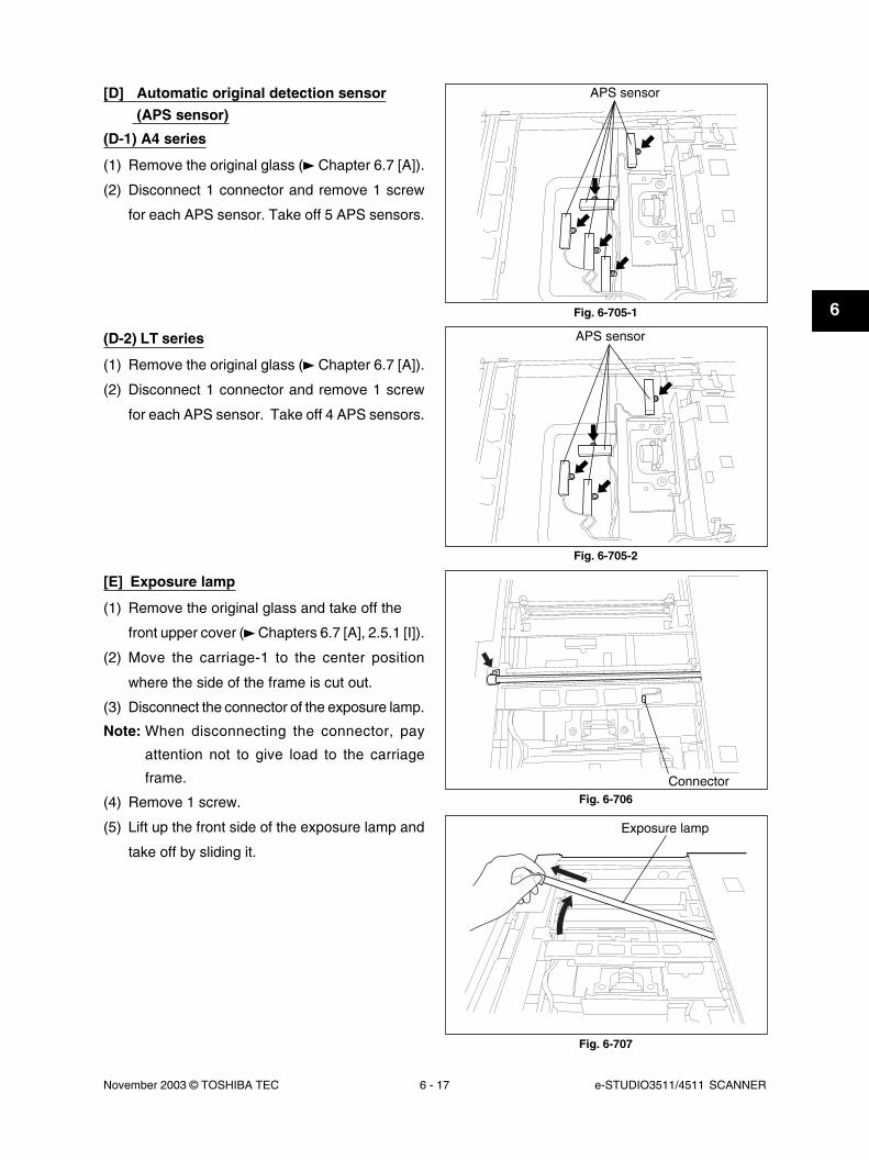
November 2003 © TOSHIBA TEC 6 - 17 e-STUDIO3511/4511 SCANNER
6
[E] Exposure lamp
(1) Remove the original glass and take off the
front upper cover ( Chapters 6.7 [A], 2.5.1 [I]).
(2) Move the carriage-1 to the center position
where the side of the frame is cut out.
(3) Disconnect the connector of the exposure lamp.
Note: When disconnecting the connector, pay
attention not to give load to the carriage
frame.
(4) Remove 1 screw.
(5) Lift up the front side of the exposure lamp and
take off by sliding it.
(D-2) LT series
(1) Remove the original glass ( Chapter 6.7 [A]).
(2) Disconnect 1 connector and remove 1 screw
for each APS sensor. Take off 4 APS sensors.
APS sensor
Connector
Exposure lamp
[D] Automatic original detection sensor(APS sensor)
(D-1) A4 series
(1) Remove the original glass ( Chapter 6.7 [A]).
(2) Disconnect 1 connector and remove 1 screw
for each APS sensor. Take off 5 APS sensors.
APS sensor
Fig. 6-705-1
Fig. 6-705-2
Fig. 6-706
Fig. 6-707

e-STUDIO3511/4511 SCANNER 6 - 18 November 2003 © TOSHIBA TEC
6
[Rear side]
[Front side]
Lens
Adjusted area
in the Service Handbook.
3. Do not touch 4 screws shown with the
arrows when replacing the lens unit.
[F] Lens unit
(1) Remove the lens cover ( Chapter 6.7 [B]).
(2) Disconnect 1 connector and remove 5 screws.
Then remove 2 screws and 2 ground wires and
take off the lens unit.
Notes:1. When installing the lens unit, fix it while
pushing it to the direction of the white
arrow.
2. For adjustment, refer to “3.9.2 Lens Unit”
Lens unit
Groundwire
Fig. 6-708
[G] Scan motor
(1) Take off the upper rear cover ( Chapter 2.5.1
[Q]).
(2) Take off the rear cover ( Chapter 2.5.1 [P]).
(3) Disconnect 1 connector.
Connector
Fig. 6-709
4. Handle the unit with care. Do not touch
the adjusted area and lens. (Hold the unit
as the right figure.)
Fig. 6-710
Fig. 6-711
Scan motor

November 2003 © TOSHIBA TEC 6 - 19 e-STUDIO3511/4511 SCANNER
6
[H] Carriages-1 and -2
(1) Remove the original glass and take off the
upper rear cover ( Chapters 6.7 [A], 2.5.1 [Q]).
(2) Move the carriage and position the holes of the
carriage to the holes of the frame.
(3) Remove 2 screws and take off the brackets
fixing the carriage-1 to the wire.
Carriage-1
(4) Remove 3 screws and take off the scan motor
with the whole bracket.
Note: When installing the scan motor, fix it with a
belt tension jig (spring).
Scan motor
Fig. 6-712
Fig. 6-714
Notes: When installing the scan motor, use the belt
tension jig (spring). The procedure is as
follows.
1. Fix the screw A.
2. Temporarily fix the screw B and C.
3. Hook the belt tension jig to the motor
bracket and the flame.
4. The scan motor is pulled by the belt
tension jig. Fix the screw B and then C at
the stopped position.
5. Remove the belt tension jig.
Fig. 6-713
Belt tension jig
A B
C
04/05

e-STUDIO3511/4511 SCANNER 6 - 20 November 2003 © TOSHIBA TEC
6
(6) Remove 2 screws and take off the inverter
board.
Mirror-1
Inverter board
Notes:1. When installing carriage-1, fix the bracket
temporarily at the position (A). Then move
it to the direction (B), push it to the end
and fix securely.
2. Refer to the Service Handbook for more
details.
(A)
(A)
(B)
Fig. 6-717
Fig. 6-718
(5) Take off the carriage-1 while inclining it.
Note: When replacing the mirror-1, replace the
carriage-1 together with mirror-1.
Mirror-1 should not be removed.
Carriage-1
Fig. 6-716
(4) Remove the square seal fixing the lamp cable
to the base. Release the harness from the
harness clamp. Disconnect the connector of the
lamp cable from the SLG board.
Fig. 6-715

November 2003 © TOSHIBA TEC 6 - 21 e-STUDIO3511/4511 SCANNER
6
Notes: 1. When installing carriage-2, fix the bracket
temporarily at the position (A). Then
move it to the direction (B), push it to the
end and fix securely.
2. Refer to the Service Handbook for more
details.
(A)
(B)
(A)
(7) Attach the wire holder jigs to the pulleys to
prevent the wires from loosening.
Note: Refer to “3.9 Adjustment of the Scanner
Section” in the Service Handbook for the
direction of the wire holder jigs.
(8) Detach the tension springs of the front and rear
sides.
(9) Remove the carriage wires.
Tension springCarriage wire
Fig. 6-719
(10) Take off the carriage-2 while its corner is
pushed into the window of the rail and inclining
the carriage.
Note: When replacing the mirrors-2 and -3, replace
the carriage-2 together with mirrors-2 and -3.
Mirrors-2 and -3 should not be removed.
Carriage-2
Fig. 6-720
Fig. 6-721
Fig. 6-722

e-STUDIO3511/4511 SCANNER 6 - 22 November 2003 © TOSHIBA TEC
6
[I] Platen sensor
(1) Take off the upper rear cover ( Chapter 2.5.1
[Q]).
(2) Disconnect 1 connector. Release the latches
and take off the platen sensor.
Platen sensor
Carriage home position sensor
Fig. 6-723
[J] Carriage home position sensor
(1) Take off the upper rear cover ( Chapter 2.5.1
[Q]).
(2) Disconnect 1 connector. Release the latches
and take off the carriage home position sensor.
[K] Scanning section control PC board
(SLG board)
(1) Take off the lens cover ( Chapter 6.7 [B]).
(2) Disconnect 7 connectors, remove 6 screws and
take off the SLG board.
SLG board
Fig. 6-724

November 2003 © TOSHIBA TEC 7 - 1 e-STUDIO3511/4511 IMAGE PROCESSING
7
7. IMAGE PROCESSING
7.1 General DescriptionThe following diagram shows the process of this equipment from scanning of original to writing data on
the photoconductive drum surface.
The followings are the boards used for image processing.
Image processing/writing control
section[LGC]
Image processing section
Photocon-ductivedrum
Imageprocessing /
System board[SYS]
Scanningcontrol section
[SLG]
Scanning section
Original
Original glass
Scanningsection[CCD]
Semicon-ductive laserelement
Laser controlsection[LDR]
Writing section
Fig. 7-101
Board
SYS board
(PWA-F-SYS-350)
LGC board
(PWA-F-LGC-350)
PPC
PRT/
SCN
ACS, color conversion, high quality image processing, image memory
editing, rectangular area signal generation, editing processing, gamma
correction, gradation processing, compression/expansion and black
component generation
Scanner high quality image processing, printer high quality image
processing, black over print, pure black/pure gray, chroma adjustment
and brightness adjustment
Function
Smoothing processing, image area control and laser related control
Lens

e-STUDIO3511/4511 IMAGE PROCESSING 7 - 2 November 2003 © TOSHIBA TEC
7
Image of an original placed on the original glass is scanned by the optical system. The CCD (Charge
Coupled Device) reads the optical image signals and converts them into the electrical signals. The
electrical signals are amplified and undergo analog-to-digital conversion, then are changed into digital
signals. Shading correction (correction of variance in CCD elements and the light source) is performed
and the digital signal is output as an image signal from the scanning section.
CCD A/Dconversion
Shadingcorrection
Signalamplification (Next process)
Fig. 7-102
The image processing section inputs the image signal from the scanning section and applies various
image processing on the signal, then transmits the output result to the writing section.
Images are processed by the SYS board (PWA-F-SYS-350) and LGC board (PWA-F-LGC-350) in this
equipment. Also, the image signals read with the Scanning Function and the printer image signals are
processed in the SYS board.

November 2003 © TOSHIBA TEC 7 - 3 e-STUDIO3511/4511 IMAGE PROCESSING
7
7.2 ConfigurationThe Fig. 7-201 shows the image processing section of this equipment.
Fig. 7-201
ASIC
ASIC
CCD
CCD board(PWA-F-CCD-350)
SLG board(PWA-F-SLG-350)
SYS board(PWA-F-SYS-350)
A/D conversion
Shading correction3-line correction
External port
Image processingsection
Page memory control
Scanner/Printer Controller
Black over printPure black/Pure grayChrome adjustment
Brightness adjustment
ACSColor conversion
Black component generationHigh quality image processing
Image memory editingEditing processing
Rectangular are signal generationEditing processing
Gamma correctionGradation processing
Compression/expansion
Scanner high quality image processingPrinter high quality image processing
ASIC
LGC board(PWA-F-LGC-350)
Laser related controlSmoothing processing
ASIC
LDR board(PWA-F-LDR-350)
Laser drive
: Image data flow
ASIC

e-STUDIO3511/4511 IMAGE PROCESSING 7 - 4 November 2003 © TOSHIBA TEC
7
7.3 SYS Board (PWA-F-SYS-350)7.3.1 Features
(1) The image processing section on the SYS board is controlled by the CPU on the SYS board.
(2) The image processing section on the SYS board realizes the following when functioning the copier:
• ACS
• Color conversion (CMY image data processing)
• Black component generation
• High quality image processing
• Image memory editing
• Rectangular area signal generation
• Editing processing
• Gamma correction
• Gradation processing
• Compression/expansion
(3) The image processing section on the SYS board realizes the following when functioning the scanner
and printer:
• Scanner high quality image processing
• Printer high quality image processing
• Black over print (Post Script)
• Pure black / Pure gray (Post Script)
• Chroma adjustment (PCL5C)
• Brightness adjustment (PCL5C)

November 2003 © TOSHIBA TEC 7 - 5 e-STUDIO3511/4511 IMAGE PROCESSING
7
7.3.2 Functions of image processing circuit
The image processing section on the SYS board realizes the followings:
(1) ACS (Auto Color Selection)
This function determines whether the original to be scanned is colored or monochrome, based on
the analysis of the R, G and B signals output from the CCD.
(2) Color conversion (CMY image data processing)
When functioning the copier, the RGB image data is converted to CMY image data. (When functioning
the scanner, it is converted to RGB image data.)
The image data taken in by the scanner represents the intensities of reflection from the three primary
colors of light (Red, Green and Blue). These RGB values are then color-converted to the respective
amounts of toners corresponding to the three colors (Yellow, Magenta and Cyan) for printing (=CMY
image data processing).
(3) Black component generation
K (Black) signal is generated from the CMY image data. Based on this K signal, the CMY image data
is corrected to suppress hue on reproducing grays or to make the black look more real.
(4) High quality image processing
(a) Background processing function
By using the background adjustment function while manually adjusting the image density,
undesirable background of the original can be removed if any, and some necessary but
disappeared background can be recovered. By using this function, it is possible to cut the
background density down when copying originals which have a certain level of background density,
such as newspapers.
<Example>
DensityLower Higher DensityLower Higher
Back-ground
Text
Larg
erN
o. o
f pix
els
Sm
alle
r
Larg
erN
o. o
f pix
els
Sm
alle
r
Histogram
Fig. 7-301
(b) Image discrimination
By determining the magnitude of density variation in a block (n x n dot), the target pixels are
judged whether they are text or photograph. If they are determined to be text, they are further
judged whether they are black or color text, using the differences in the levels of CMY signals.
After backgroundprocessing
Dynamic rangewidth
Extended dynamicrange width

e-STUDIO3511/4511 IMAGE PROCESSING 7 - 6 November 2003 © TOSHIBA TEC
7
0 1 2 3 4 5 6 7 8 9 0 1 2 3 4 5 6 7 8 9
(c) Filtering
This function is enabled by low-pass filter processing and high-pass filter processing.
• Low-pass filter processing
This processing removes image/electrical noise and decreases moire by performing averaging
operation between the image signals of the targeted pixel and those of the neighboring pixels
to enhance the reproducibility of original.
<Example> Density of the targeted pixel position is X. Density of pixel positions at front and
back of the targeted pixel are “a” and “b” respectively. X is converted to X’ through
the low pass filtering.
When the matrix is (3 x 1):
The above averaging operation is performed for all the pixels to accomplish the high
reproducibility of original.
(The following is the case that the low pass filtering is applied on the primary scanning pixel.)
Fig. 7-302
• High-pass filter processing
Character outline blurs when the original, such as text, with big difference in density among the
pixels is optically scanned and output from the CCD. Characteristic of the lens and other factors
cause this phenomenon. In this equipment, processing such as edge enhancement is applied
between the targeted pixel and the neighboring pixels to eliminate this phenomenon and realize
high reproducibility of original.
Density
After low-pass filter
Primary scanning pixel positions
a + b + x3
x’ =
Solid black area
Density
Primary scanning pixel positions
a x b
Fig. 7-303
Original
Image signal
After correction
Low contrast area

November 2003 © TOSHIBA TEC 7 - 7 e-STUDIO3511/4511 IMAGE PROCESSING
7
(5) Image memory editing
This function performs editing such as enlargement/reduction, mirror imaging, etc., by using a line
memory. Pixel data for one line in the primary scanning direction is stored in the line memory and the
memory is renewed at each line.
(a) Enlargement/Reduction
Enlargment/Reduction is accomplished by using the line memory control function in the process
of the image processing operation.
<Example> Enlargement
<Example> Reduction
(b) Mirror imaging
This is accomplished by reading and outputting data from its end.
(6) Rectangular area signal generation
When a rectangular coordinate position is selected, the corresponding rectangular area signals are
generated. Using these signals, various edit processing related to the area specification can be
performed.
(7) Editing processing
This function performs trimming and masking.
(a) Trimming
Using rectangular area signals, the image signals inside the rectangular area are left and the
other image signals are eliminated.
(b) Masking
Using rectangular area signals, the image data inside the rectangular area are erased.
1100%
200%
2 3 4 5 6 7 8 9 10
1 1 2 2 3 3 4 4 5 5
1100%
50%
2 3 4 5 6 7 8 9 10
1 3 5 7 9
Fig. 7-304

e-STUDIO3511/4511 IMAGE PROCESSING 7 - 8 November 2003 © TOSHIBA TEC
7
Fig. 7-305
Ideal image Out of color registration Black over print
Black data Black data Black data
Background Background
Background PaperPaperPaper
(8) Gamma correction
This function corrects the input/output characteristics of the scanner/printer and adjusts the image
signals so that the input/output characteristics would match with the copy mode.
(9) Gradation processing
In case of color copying, this function switches the type of gradation processing depending on the
copy mode: A type which selects the printer characteristics giving the priority to resolution such as
for text data, and another which selects the printer characteristics giving the priority to reproducibility
of gradation such as for photographic images.
In case of black copying, this function selects the gradation processing which reproduces the halftone
image such as photograph more precisely. Also the gradation processing which makes text data
clearer is selected in black copying mode.
(10) Compression/expansion
To lessen the data amount of the color image signals, this function effects the compression/expansion
on the data.
(11) Scanner high quality image processing
This function corrects the image signals scanned by the scanner and reproduces them in a higher
image quality.
(12) Printer high quality image processing
This function reproduces the image signals output from the printer controller in a higher image
quality.
(13) Black over print (Post Script)
When black data of text or graphic object are formed on a certain background with no written data
underneath them, the color of the paper comes out around the black data when “out-of-color
registration” is occurring. To prevent this phenomenon, this process enables to keep the background
color around the black data formed as a part of the text or the graphic object on the printer data.

November 2003 © TOSHIBA TEC 7 - 9 e-STUDIO3511/4511 IMAGE PROCESSING
7
(14) Pure black/Pure gray (Post Script)
This function is to printout the text and graphics formed as black data with black toner only on the
printer data, not using 4 color toner. The gray text/graphics are also printed out with black toner only.
(15) Chroma adjustment (PCL5C)
This function adjusts chromaticness of the printer data.
(16) Brightness adjustment (PCL5C)
This function adjusts brightness of the printer data.

e-STUDIO3511/4511 IMAGE PROCESSING 7 - 10 November 2003 © TOSHIBA TEC
7
7.4 LGC Board (PWA-F-LGC-350)7.4.1 Features
(1) The image processing ASIC on the LGC board is controlled by CPU mounted on the LGC board.
(2) The image processing functions of the LGC board realizes the followings:
• Smoothing processing
• Image area control
• Laser related control
7.4.2 Functions of image processing circuit
An image processing ASIC mounted on the LGC board enables the following functions:
(1) Smoothing processing
This function removes jaggy and smoothes character outline of images and output them.
(2) Image area control
This function sets the effective image area in horizontal and vertical directions to be output.
(3) Laser related control
This function performs the APC (Auto Power Control).
7.5 Laser Driving PC Board (LDR Board)Image signals processed on the LGC board are processed by ASIC for writing control and LDR board.
The signal is then laser controlled and written on the drum.
(1) Setting of effective image area ......................... • Top, bottom, left and right margins
(2) Horizontal synchronization signal (HSYNC) ..... • Reference clock signal in the printer section
clock generation section synchronized with HSYNC and its signal.
(3) Laser drive section ........................................... • ON/OFF control of the semiconductive laser and
APC (Auto Power Control).

November 2003 © TOSHIBA TEC 8 - 1 e-STUDIO3511/4511 LASER OPTICAL UNIT
8
8. LASER OPTICAL UNIT
8.1 General DescriptionThe laser optical unit radiates the laser beam onto the photoconductive drum responding to the digital
image signals transmitted from the scanner, printer controller, etc. to create the latent image. Image
signal is converted into the light emission signal of the laser diode on the laser driving PC board, then
radiated on the drum through the optical elements such as cylinder lenses, polygonal mirror and fθθθθθ lens.
The unit must not be disassembled in the field as they are very sensitive to dust and finely adjusted at the
factory.
[Laser Optical Unit Overview]
Fig. 8-101

e-STUDIO3511/4511 LASER OPTICAL UNIT 8 - 2 November 2003 © TOSHIBA TEC
8
Mirror
Polygonal motor
Cylinder lens
Finite focus lens
Aperture
LDR board
[Writing Section Overview]
Fig. 8-102
Slit glass(for outgoing laser beam)
SNS board
fθ lens 2
fθ lens 1

November 2003 © TOSHIBA TEC 8 - 3 e-STUDIO3511/4511 LASER OPTICAL UNIT
8
8.2 Structure(1) Laser emission Unit
This unit consists of the laser diode, finite focus lens, aperture and cylinder lens.
a. Laser diode
This laser diode features low droop, small laser variation and low threshold current.
Aperture determines the shape of the laser beam at laser emission position of the primary scan-
ning and secondary scanning.
Laser diode radiates the laser beams responding to the laser emission control (ON/OFF) signals
from the laser driving PC board. Laser beams which passed through the finite focus lens are
focused on the drum surface.
b. CAUTION
The beam of the semiconductor laser is very weak (about 10 mW), but focused parallel rays
creates great energy which is hazardous.
Some materials of the components of the laser optical unit are metal. Since the unit is in a sealed
container, there is no danger of laser leakage during normal operation.
Note: Laser beam is not visible. Pay the closest attention when handling the laser unit compo-
nents or performing operations such as adjustment of the laser beam, and this kind of
operations are very dangerous and must be performed only by specially trained staff.
The warning label shown below is attached on the left side of the upper inner cover.
Fig. 8-201
[CAUTION]
• Do not approach tools near the path of the laser beam.
• Take off your watches, rings, bracelets, etc. before handling the unit.

e-STUDIO3511/4511 LASER OPTICAL UNIT 8 - 4 November 2003 © TOSHIBA TEC
8
(2) Polygonal motor unit
This unit consists of the polygonal motor,
polygonal mirror and polygonal mirror cover.
a. Polygonal motor
This motor rotates the polygonal mirror in high
speed.
The DC motor controls the rotation speed of
the mirror motor as follows:
During ready : 10,000.00 rpm
During printing : 36,734.37 rpm (600dpi)
: 37,322.12 rpm
(FAX 15.4x16.0dot/mm)
: 35,922.54 rpm
(FAX 16.0x15.4dot/mm)
b. Polygonal mirror
One laser beam emitted from the laser diode
is reflected by this mirror. As the polygonal
mirror is rotated by the polygonal motor, the
reflected laser light moves in sync with the
rotation. The direction of the movement is the
primary scanning direction of the image. One
scan is performed on one plane of the polygonal
mirror.
As the polygonal mirror has eight planes, eight
scans are performed in one rotation of the
polygonal mirror.
c. Polygonal mirror cover
Polygonal mirror cover reduces the windage
loss and noise, prevents adhesion of foreign
matters onto the mirror surface and releases
heat.One scan is completed by completion of steps (A) to (C).One scan is performed on one plane of the polygonal-mirror. Eight scans can be made with one rotation of thepolygonal mirror.
Laser light
Drum
Laser light
Drum
Laser light
Drum
Fig. 8-202
(B)
(A)
(C)

November 2003 © TOSHIBA TEC 8 - 5 e-STUDIO3511/4511 LASER OPTICAL UNIT
8
(3) fθθθθθ lenses 1 and 2
These two lenses perform the following adjustment on the laser beams reflected by the polygonal
mirror.
a. Uniform-velocity scanning
Since the polygonal mirror is rotating at a
uniform velocity, the laser beam reflected
from the mirror scans over the drum surface
at a uniform angular velocity; namely, the
pitch between the dots on the drum is wider
at both ends than at the center of the
scanning range. The fθθθθθ lenses help to correct
this difference, making all the dot-to-dot
pitches equal on the drum surface.
b. Face tilt correction
The reflecting face of the polygonal mirror is
tilted slightly to one side against the perfect
vertical. Horizontal deviation of the laser light
which is caused by the tilt is corrected.
c. Sectional shape of laser beam
The shape of the laser beam spotted on the
drum is adjusted.
Wider
Narrower
Drum
fθθθθθ Lens 2
Same intervals
Mirror plane is tilted. Deviation
(4) H-Sync signal detection PC board (SNS board)
The laser light which is started to be scanned from one of the reflected plane of the polygonal mirror
is reflected by the H-Sync detection mirror and enters the PIN diode on the H-Sync signal detection
PC board. The primary scanning synchronizing signal is generated based on this reflection.
Fig. 8-203
Fig. 8-204
fθθθθθ Lens 1

e-STUDIO3511/4511 LASER OPTICAL UNIT 8 - 6 November 2003 © TOSHIBA TEC
8
(5) Laser driving PC board (LDR board)
This control board has the following functions:
a. APC control function (adjusts disparity of the laser intensity caused by temperature)
b. Laser ON/OFF function
(6) Slit glass
Slit glass is located where the laser beams are output from the laser optical unit, and it protects the
unit from dust.

November 2003 © TOSHIBA TEC 8 - 7 e-STUDIO3511/4511 LASER OPTICAL UNIT
8
Fig. 8-302
Fig. 8-302 shows a block diagram of the semiconductive laser control circuit. The semiconductive laser
performs monitor efficiency regulation (a process to control monitor current for the light amount), and
laser itself is adjusted to initial output emission of approx. 3.0 mW (approx. 408 µW on the drum surface).
The regulated voltage of the monitor output is feedback to the laser power comparison circuit. This
monitor output voltage is compared with the laser power voltage set for the control circuit for every
scanning. Laser driver circuit increases the forward current if the laser power is insufficient, and decreases
the current when the power is excessive to maintain a constant optical output.
8.3 Laser DiodeThe laser used in this equipment is a A1GaAs type semiconductive laser. It is generated in the single-
horizontal mode, and its wavelength is approx. 785 nm. This semiconductive laser outputs 10mW with
standard DC power supply. Laser intensity is controlled by using the output from the PIN diode for
monitoring light output in the semiconductive laser.
The relation between the current and optical output
of the semiconductive laser is as shown at right.
Light emission is started when the forward current
reaches or becomes larger than the threshold
current and outputs the monitor current which is
proportionate to the optical output. The threshold
current and monitor current differs depending on
each semiconductive laser. So optical output has
to be adjusted to maintain a constant value.
Since the optical output of the semiconductive laser
is decreased as the temperature of the laser rises,
APC control needs to be performed to maintain a
constant optical output.
Threshold currentO
ptic
al O
utpu
t (m
W)
Low temp.
High temp.
Forward current
Monitor current
Current (mA)
Monitor outputMonitor efficiencyregulation circuit
Laser powercomparisoncircuit
Laser drivercircuit
Semiconductive laser
Constantoptical output
Fig. 8-301
Regulation
Power source

e-STUDIO3511/4511 LASER OPTICAL UNIT 8 - 8 November 2003 © TOSHIBA TEC
8
8.4 Laser Unit Cooling FanThe laser unit cooling fan is a propeller fan (80 x 80 mm). It cools down the polygonal motor and the
Laser driving PC board.
8.5 Polygonal Motor(1) Drive circuit of the polygonal motor
(2) Control signal
The polygonal motor is a DC motor which is PLL-controlled by clock signal. The signals from LGC
board controls the polygonal motor.
Signal
POMON
POMCK
POMPL
PWA-F-LGC M/DC-POL
PD4
DCCLK4
PI1
POMON
POMCK
POMPL
LCA301-1
Gate array
Buf
fer
(IC
7407
)
Fig. 8-501
Level “L”
ON
—
Normal rotation
Level “H”
OFF
—
Abnormal rotation
Remarks
Polygonal motor ON/OFF signal
Polygonal motor reference clock signal
Polygonal motor PLL signal

November 2003 © TOSHIBA TEC 8 - 9 e-STUDIO3511/4511 LASER OPTICAL UNIT
8
(4) Take off the left cover ( Chapter 2.5.1 [F]).
(5) Remove 2 screw and take off the toner cover.
8.6 Disassembly and Replacement[A] Laser optical unit
(1) Take off the rear cover ( Chapter 2.5.1 [P]).
(2) Take off the LGC board cover ( Chapter 2.5.2
[A]).
(3) Disconnect 2 connectors and release the har-
ness from the harness clamp.
Fig. 8-601
Fig. 8-602
Connector Harness clamp
Toner cover
(6) Release the harness, loosen 2 screws and take
off the anti-vibration bracket.
(7) Pull out 2 harnesses and remove 1 screw.
(8) Pull out the laser optical unit while lifting it up
and take it off.
Fig. 8-604
Laser optical unit
Fig. 8-603
Anti-vibration bracket
Harness

e-STUDIO3511/4511 LASER OPTICAL UNIT 8 - 10 November 2003 © TOSHIBA TEC
8
(4) Disconnect 1 connector and remove 2 screws.
Take off the laser unit cooling fan.
Fig. 8-607
Laser unitcooling fan
Fig. 8-606
[B] Laser unit cooling fan
(1) Open the front cover.
(2) Remove the receiving tray ( Chapter 2.5.1
[B]).
(3) Remove 2 screws and take off the inner cover.
Inner cover
Notes:1. Do not leave fingerprints or stain on the slit glass.
2. Laser optical unit is a precise apparatus.
Handle the unit with extra care not to shock or
vibrate it.
3. Do not disassemble the unit in the field since it
is very sensitive to the dust and stain.
4. When installing the laser optical unit (installing
the harnesses), take off the left rear cover first
so that the harnesses will be easily seen and
installed (View from (A)) ( Chapter 2.5.1 [G]). Fig. 8-605
(A)

November 2003 © TOSHIBA TEC 9 - 1 e-STUDIO3511/4511 DRIVE SYSTEM
9
9. DRIVE SYSTEM
9.1 General DescriptionThis chapter explains about each drive system of the main motor, transport motor and developer motor.
The function of each drive unit is as follows:
• Main motor Photoconductive drum
Transfer belt
• Transport motor Fuser unit Bridge unit (option)
2nd transfer roller
Registration roller
Transport roller
Feed roller
Bypass feed roller
• Revolver motor Revolver unit
• Developer motor Black developer unit
Color developer unit
• ADU motor ADU
• Exit motor Exit roller
• Toner motor Black toner cartridge
• Drum cleaner brush motor Drum cleaner brush
• Transfer belt cleaner auger motor Transfer belt cleaner auger

e-STUDIO3511/4511 DRIVE SYSTEM 9 - 2 November 2003 © TOSHIBA TEC
9
(G80/P36)
(P53/G15)
(G45/G21)
(P75/P33)
(P27/G33)
(G100/P20)
(G16)
(G27/G20)
(G40/G23)
(P100)
(G19)(G27/P33)
(G31)
(G10)
9.2 Main Motor9.2.1 Construction
The main motor drive unit consists of two parts: One part transmits the drive from the main motor to
photoconductive drum and the transfer belt, and another part transmits the drive from the drum cleaner
brush motor to the drum cleaner brush.
The drive to the photoconductive drum is transmitted by the gear, timing belt and the coupling and the
drive to the transfer belt is transmitted by the gear and timing belt. The main motor is a brushless DC
motor.Main motor gear
Drum cleaner brush motor
Fig. 9-201

November 2003 © TOSHIBA TEC 9 - 3 e-STUDIO3511/4511 DRIVE SYSTEM
9
9.2.2 Drive circuit of main motor
(1) The control signal from LGC controls the operations of the main motor, such as switching of ON/OFF,
a rotational direction, a rotational speed, etc. The rotational speed is decided by clock frequency
output at the main motor. The speed is lowered to the range from 1/2 to 1/4 at the Thick Paper/OHP
Film Mode. This switching is performed between the completion of the 1st transfer and that of the
2nd transfer.
Signal Level “L” Level “H” Remarks
MAMON ON OFF Main motor ON signal
MAMBK Braking Normal Main motor brake signal
MAMCW CW CCW Main motor rotational direction signal
MAMGA Low speed High speed Main motor speed switching signal
MAMCK — — Main motor reference clock signal
MAMPL Normal Out of control Main motor PLL signal
* CCW: forward rotation CW: backward rotation
7407
62385 MAMON
MAMCW
MAMBK
MAMPL
PWA-F-LGC Main Motor
MAMCK
MAMGA
PK0
PK2
PK1
DCCLK1
PK3
Gate array
Fig. 9-202
9.2.3 Signal level of motor circuit

e-STUDIO3511/4511 DRIVE SYSTEM 9 - 4 November 2003 © TOSHIBA TEC
9
9.3 Transport Motor9.3.1 Construction
The transport motor drive unit transmits the drive from the transport motor to the fuser unit, 2nd transfer
roller, registration roller, transport roller, feed roller, bypass feed roller and bridge unit (option) through
the gears and clutches.
(G64/G30)
(G10)
(G30)(G22)
(G25/G14)(G24)
(G35/G21)(G30)
(G23)
(G28/G17)
(G28)
(G32/G35)
(G28)
(G25)
(G31/G38)
(G28)
(G28)
(G27)
(G28)
(G25/34)
(G22)
(G30)
Transport motor gear
Registration clutch
Upper transport clutch (High speed)
Upper transport clutch (Low speed)
Fig. 9-301

November 2003 © TOSHIBA TEC 9 - 5 e-STUDIO3511/4511 DRIVE SYSTEM
9
9.3.2 Drive circuit of transport motor
The transport motor is a DC brushless motor. At color printing modes with thick paper or OHP film, the
transport speed is lowered to 1/2, 1/3 or 1/4 depending on its mode for most effective fusing.
The following is the block diagram of the transport motor.
FDMCW
FDMGA
FDMON
FDMPL
PWA-F-LGC Feed Motor
7407
62385
7407
FDMCK
PJ5
PJ7
PJ6
DCCLK2
PI2
Gate array
Fig. 9-302
Signal level of motor circuit
Signal Level “H” Level “L” Remarks
FDMCW CCW CW Transport motor rotational direction signal
FDMON OFF ON Transport motor ON signal
FDMGA High speed Low speed Transport motor speed switching signal
FDMCK — — Transport motor reference clock signal
FDMPL Out of control Normal Transport motor PLL signal
* FDMCW (rotational direction signal): The motor does not rotate backward (CCW) in actual movement.

e-STUDIO3511/4511 DRIVE SYSTEM 9 - 6 November 2003 © TOSHIBA TEC
9
9.4 Developer Motor9.4.1 Construction
The developer motor is a motor drives the following movements:
(A) Lifting movement by rotating the lifting cam in the black developer unit
(B) Rotational movement of magnet roller in the black developer unit
(C) Rotational movement of toner supply auger in the color developer unit
(D) Rotational movement of magnet roller in the color developer unit
Each movement is performed by drive transmission from the developer motor through the gears and
clutches.
The revolver unit contains three color developer units. The developer motor drives the color developer
unit only at the developing position; it means each developer unit does not have its own drive. When the
revolver rotates, the clutch turns OFF so that the drive of the developer motor will not be transmitted and
a damage to the gear will be prevented.
(G27) (G46/G24)
(G43)
(G48)
(G46/G24)
(G15)
(G17)
(G28)
(G/33/G16)
(G29)
(G28)
(G28)
(G28)
(G28)
(G10)
(G19)
(G17)
(C)Color developer toner supply clutch
(D)Color developer drive clutch
(A)Black developer lifting clutch
(B)Black developer drive clutch
Developer motor gear
Fig. 9-401

November 2003 © TOSHIBA TEC 9 - 7 e-STUDIO3511/4511 DRIVE SYSTEM
9
9.4.2 Drive circuit of developer motor
7407
62385 DVMON
DVMCK
DVMCW
DVMPL
PWA-F-LGC Developer Motor
Gate array
Fig. 9-402
(1) LGC board provides a signal to control the rotation of the developer motor.
(DVMON: Developer motor ON signal)
When signal from LGC board is the level "L", the developer motor stops.
(2) DVMCW signal controls the rotational direction of the motor. The motor rotates forward (CCW) but
does not rotate backward (CW) in actual movement. Namely, DVMCW signal is always output level
"H".
Signal level of motor circuit
Signal Level “L” Level “H” Remarks
DVMON ON OFF Developer motor ON signal
DVMCW CW CCW Developer motor rotational direction signal
DVMCK — — Developer motor reference clock signal
DVMPL Normal Out of control Developer motor PLL signal

e-STUDIO3511/4511 DRIVE SYSTEM 9 - 8 November 2003 © TOSHIBA TEC
9
(5) Remove 3 screws and take off the bracket.
9.5 Disassembly and Replacement[A] Developer motor drive unit
(1) Take off the rear cover ( Chapter 2.5.1 [P]).
(2) Take off the LGC board, SYS board and
switching power supply with the whole case
( Chapter 2.5.2 [A] [C] [E]).
(3) Remove 3 screws and take off the flywheel.
Note: The main motor can be taken off by itself
without removing the drive unit. (2 screws
and 1 connector)
(4) Remove 2 screws and take off the bracket.
(6) Disconnect 3 connectors and remove 5 screws.
Release the harnesses from 3 harness clamps.
Take off the developer motor drive unit.
Fig. 9-501
Fig. 9-502
Fig. 9-503
Fig. 9-504
Flywheel
Main motor
Bracket
Bracket
ConnectorDeveloper motor drive unit
04/05

November 2003 © TOSHIBA TEC 9 - 9 e-STUDIO3511/4511 DRIVE SYSTEM
9
(A-1) Developer motor
(1) Remove 2 screws and take off the developer
motor.
(A-2) Black developer lifting clutch
(1) Remove 4 screws and take off the bracket.
(A-3) Color developer toner supply clutch, color
developer drive clutch and black developer
drive clutch
(1) Remove 3 screws, 2 clips, 2 bushing, release
the harness from 3 harness clamps and take
off the bracket.
Fig. 9-505
Fig. 9-506
Fig. 9-507
Fig. 9-508
Developer motor
Bracket
Clutch
Bracket
Clip, bushing
Harnessclamp
Harnessclamp
(2) Take off the black developer lifting clutch.
Note: Place the stopper when installing the clutch.

e-STUDIO3511/4511 DRIVE SYSTEM 9 - 10 November 2003 © TOSHIBA TEC
9
(2) Remove the gear, E-ring and the clip of each
clutch.
(3) Disconnect 1 connector and take off the color
developer toner supply clutch.
(4) Remove clip A and gear C. Remove 1 bushing
and clip B. Disconnect 1 connector and take
off the color developer drive clutch.
(5) Disconnect 1 connector and take off the black
developer drive clutch.
[B] Transport motor drive unit
(1) Take off the rear cover and right rear cover
( Chapter 2.5.1 [P] [L]).
(2) Take off the LGC board and the SYS board with
the whole case ( Chapter 2.5.2 [A] [C]).
(3) Remove 3 screws and take off the flywheel
( Chapter 9.5 [A]).
(4) Take off IH control PC board with the whole
cover ( Chapter 16.7 [M]).
(5) Take off the ozone exhaust fan with the whole
cover ( Chapter 11.7 [J]).
(6) Remove 2 screws and take off the ozone
exhaust duct.
(7) Remove 2 screws and take off the bracket.
Fig. 9-509
Fig. 9-510
Fig. 9-511
Gear and clip
Gear C
Clip A
Color developerdrive clutch
Clip BBushing
Black developer drive clutch
Color developer toner supply clutch
Bracket
Ozone exhaustduct
Gear and E-ring
Gear

November 2003 © TOSHIBA TEC 9 - 11 e-STUDIO3511/4511 DRIVE SYSTEM
9
(9) Take off the fuser unit ( Chapter 16.7 [A]).
(10) Remove 1 screw and take off the bracket.
(11) Loosen 1 setscrew, disconnect 1 connector
and take off the registration clutch.
(12) Remove 2 screws and take off the clutch fixing
cover.
Notes: 1. Make sure not to take off the fixing
cover completely. Stand the fixing
cover against the equipment being
connected with the harness.
Fig. 9-513
Fig. 9-514
Fig. 9-512
Bracket
(8) Remove 2 screws and take off the bracket.
Bracket
Registrationclutch
Setscrew
Fixing cover
2. When the registration clutch is
reassembled, assemble by keeping the
end of the shaft match with the end of
the clutch.
Fig. 9-515
0

e-STUDIO3511/4511 DRIVE SYSTEM 9 - 12 November 2003 © TOSHIBA TEC
9
(15) Remove 2 screws and take off the transport
motor.
(16) Remove 2 screws and take off the bracket,
and then take off the upper transport clutch
(low speed).
(17) Remove 9 screws and take off the cover of
transport gear drive unit.
Fig. 9-518
Fig. 9-519
(14) Disconnect 2 connectors and remove 5 screws.
Take off the transport motor drive unit.
Fig. 9-517
Transport motor drive unit
Transport motor
Upper transport clutch (Low speed)
(13) Loosen 1 setscrew, disconnect 1 connector
and take off the upper transport clutch (high
speed) with the gear.
Note: Do not mix up the registration clutch and
upper transport clutch (high speed) when
installing.
Fig. 9-516
Upper transport clutch(High speed)
Setscrew
Connector
Connector
Bracket
Cover

November 2003 © TOSHIBA TEC 9 - 13 e-STUDIO3511/4511 DRIVE SYSTEM
9
(9) Disconnect 2 connectors, release 2 harness
clamps and remove 6 screws.
Take off the main motor drive unit.
(10) Remove 4 screws and take off the main motor.
Note: When taking off only the main motor, it can
be taken off by removing the LGC board and
SYS board with the whole case.
Fig. 9-521
Fig. 9-522
[C] Main motor drive unit
(1) Take off the cleaner unit ( Chapter 11.7 [A]).
(2) Take off the rear cover ( Chapter 2.5.1 [P]).
(3) Take off the LGC board and the SYS board with
the whole case ( Chapter 2.5.2 [A] [C]).
(4) Remove 3 screws and take off the flywheel
( Chapter 9.5 [A]).
(5) Take off IH control PC board with the whole
cover ( Chapter 16.7 [M]).
(6) Take off the ozone exhaust fan with the whole
cover ( Chapter 11.7 [J]).
(7) Remove 2 screws take off the ozone exhaust
duct ( Chapter 9.5 [B]).
(8) Remove 4 screws and take off the bracket.
Note: This step can be omitted if the developer
motor drive unit and the transport motor drive
unit are already taken out.
Fig. 9-520
Main motor drive unit
Main motor
Harness clamp
Connector
Harness clamp
Connector

e-STUDIO3511/4511 DRIVE SYSTEM 9 - 14 November 2003 © TOSHIBA TEC
9
(12) Remove clip A (back side of the unit), gear A
with the shaft and 2 bushings. Remove clip B
(back side of the unit), gear B with the shaft, 2
bushings, and gear C between the metal plates
of the drive unit.
Fig. 9-524
(13) Remove 8 screws (denoted with the white
arrows are the plastic screws) and take off
the plate cover.
Fig. 9-525
Fig. 9-526
Clip A
Clip B
Gear B
Gear CGear A
Clip B
Plate cover
(11) Loosen 1 screw, shift the tension plate to the
direction of the white arrow, and then fix it at
the position where the belt tension is loosened.
Fig. 9-523
Tension plate

November 2003 © TOSHIBA TEC 9 - 15 e-STUDIO3511/4511 DRIVE SYSTEM
9
(14) Remove 2 screws and take off the drum
cleaner brush motor.
Notes: 1. When reassembling the unit, make sure
to follow the inverse procedure of
disassembling.
2. Make sure to assemble the unit while all
the belt tensions are loosened. Tense the
belts after reassembling.
3. Rotate the rotor section of the motor for
several times by hand to shake down the
belt while the belt is tense. Then screw
the belt tensioner.
Fig. 9-527
Drum cleaner brushmotor

e-STUDIO3511/4511 DRIVE SYSTEM 9 - 16 November 2003 © TOSHIBA TEC
9

November 2003 © TOSHIBA TEC 10 - 1 e-STUDIO3511/4511 PAPER FEEDING SYSTEM
10
10. PAPER FEEDING SYSTEM
10.1 General DescriptionsThis chapter explains how the system works to pick up paper from the drawer or bypass tray and transport
it to the transfer unit.
The paper feeding system mainly consists of the pickup roller, feed roller, separation roller, transport
roller, registration roller, bypass paper sensor, empty sensor, paper stock sensor, feed sensor, registration
sensor and drive system for these components. The transport motor drives the above rollers and sensors.
Refer to chapter 9 for more details about the transport motor and its drive system.
(1) Pickup roller (Drawers and bypass feed)
This roller moves up and down and draws out the paper from the bypass tray or drawer and transport
it to the feed roller.
(2) Feed roller (Drawers and bypass feed)
This roller is placed against the separation roller. It transports the paper from the pickup roller to the
transport roller.
(3) Separation roller (Drawers and bypass feed)
This roller is placed against the feed roller. When two sheets of paper or more are transported from
the pickup roller, the load of the torque limiter of the separation roller is heavier than the frictional
force between the sheets. As the result, the separation roller is stopped and the lower paper is not
advanced any further. When only one sheet is transported from the pickup roller, the separation
roller rotates following the feed roller.
(4) Transport roller (Drawers and bypass feed)
This roller transports the paper sent from the feed roller to the registration roller.
(5) Registration roller
Paper transported from the transport roller is pushed against the registration roller which aligns the
leading edge of the paper.
Then, the registration rollers rotate to transport the paper to the transfer unit.
e-STUDIO3511/4511 PAPER FEEDING SYSTEM 10 - 2 November 2003 © TOSHIBA TEC
10
The followings are about sensors which detect paper size, availability of paper and position of the paper
being transported to control ON/OFF of the rollers.
(6) Bypass paper sensor
This sensor detects if paper is set in the bypass tray. If it is, bypass feeding always comes before
drawer feeding.
(7) Empty sensor (Upper/Lower drawer)
This is a transmissive-type sensor and detects the availability of paper in the drawer by using an
actuator. When there is no paper in the drawer, the actuator blocks the light path of the sensor, and
the sensor determines that there is no paper.
(8) Paper stock sensor (Upper/Lower drawer)
This is a transmissive-type sensor which detects the amount of the remaining paper in the drawer
using an actuator. When the remaining paper is consumed and becomes around 100 sheets, the
actuator blocks the light path for the transmissive-type sensor to notify that the paper is getting fewer.
(9) Feed sensor (Upper/Lower drawer and bypass feed)
This sensor detects if the leading edge or trailing edge of the paper has passed the feed roller. It also
detects jamming such as misfeeding.
(10) Registration sensor
This sensor detects that the leading edge of the paper has reached the registration roller and the
trailing edge of the paper has passed the registration roller.

November 2003 © TOSHIBA TEC 10 - 3 e-STUDIO3511/4511 PAPER FEEDING SYSTEM
10
Paper Feeding Section Sectional View (Front side)
Fig. 10-101
No. Name
1 Bypass feed roller
2 Bypass separation roller
3 Bypass pickup roller
4 Upper drawer feed roller
5 Upper drawer separation roller
6 Upper drawer pickup roller
7 Transport roller
8 Lower drawer feed roller
9 Lower drawer separation roller
No. Name
10 Lower drawer pickup roller
11 Bypass paper sensor
12 Registration sensor
13 Registration roller (rubber roller)
14 Registration roller (metal roller)
15 Upper drawer feed sensor
16 Lower drawer feed sensor
17 Bypass feed sensor
1
2
3
4
5
6
7
7
7
8
9
10
11
12 1314
1516
17
7
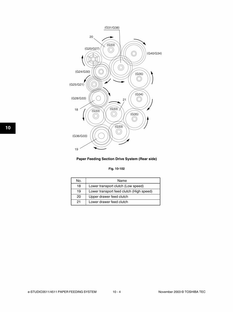
e-STUDIO3511/4511 PAPER FEEDING SYSTEM 10 - 4 November 2003 © TOSHIBA TEC
10
Paper Feeding Section Drive System (Rear side)
Fig. 10-102
No. Name
18 Lower transport clutch (Low speed)
19 Lower transport feed clutch (High speed)
20 Upper drawer feed clutch
21 Lower drawer feed clutch
(G40/G34)
(G35)
(G34)
(G35)
(G33)
(G33)
(G33)
(G31/G38)
(G20/G27)
(G24/G30)
(G25/G21)
(G33)
(G28/G33)
(G36/G33)
18
21
20
19
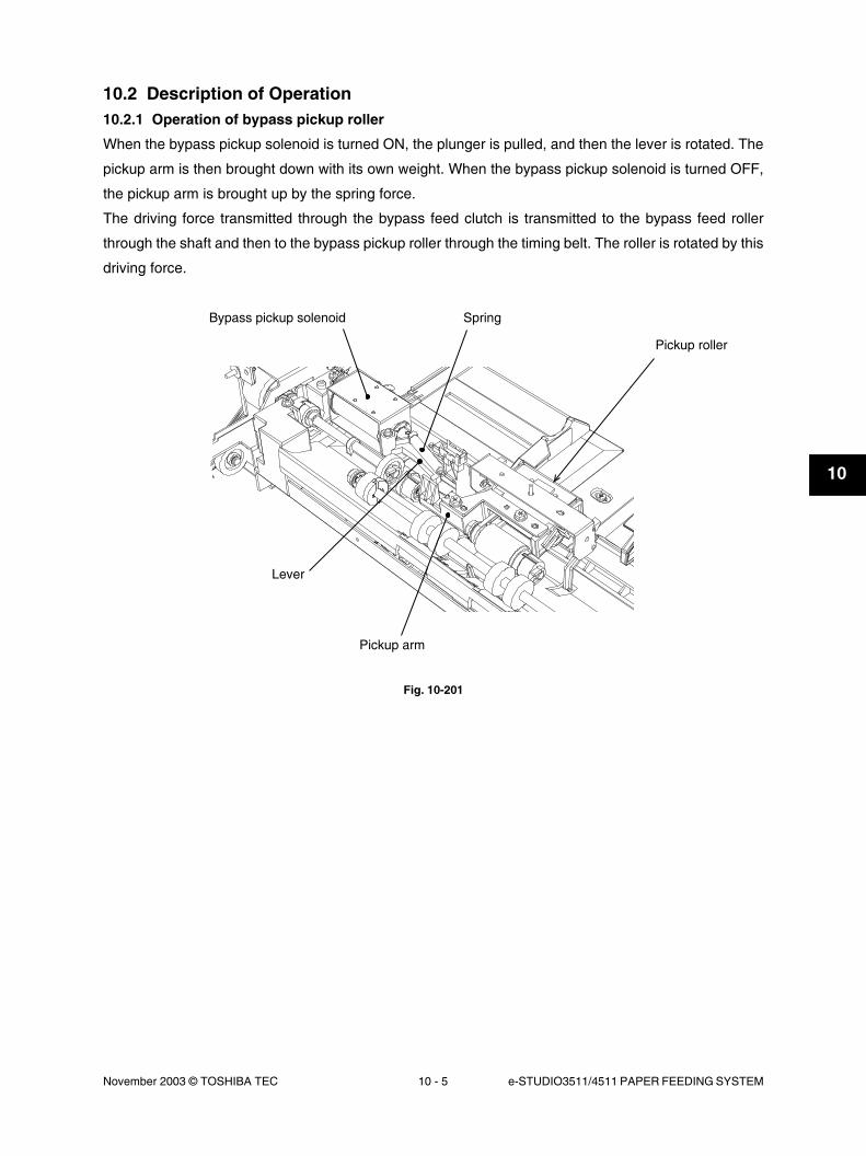
November 2003 © TOSHIBA TEC 10 - 5 e-STUDIO3511/4511 PAPER FEEDING SYSTEM
10
10.2 Description of Operation10.2.1 Operation of bypass pickup roller
When the bypass pickup solenoid is turned ON, the plunger is pulled, and then the lever is rotated. The
pickup arm is then brought down with its own weight. When the bypass pickup solenoid is turned OFF,
the pickup arm is brought up by the spring force.
The driving force transmitted through the bypass feed clutch is transmitted to the bypass feed roller
through the shaft and then to the bypass pickup roller through the timing belt. The roller is rotated by this
driving force.
Spring
Pickup roller
Bypass pickup solenoid
Lever
Pickup arm
Fig. 10-201

e-STUDIO3511/4511 PAPER FEEDING SYSTEM 10 - 6 November 2003 © TOSHIBA TEC
10 A
Insertion direction
Lever (a) Pickup rollerA
10.2.2 Operation of drawer pickup roller
When the drawer is inserted, the protrusion at the rear side of the drawer moves up the lever (a) to the
direction of A. The pickup roller and roller holder are then lowered by it's own weight.
Fig. 10-202

November 2003 © TOSHIBA TEC 10 - 7 e-STUDIO3511/4511 PAPER FEEDING SYSTEM
10
10.2.3 Separation of paper
The separation roller in this equipment works to separate the sheets being fed. The separation roller unit
consists of the feed roller, separation roller, spring joint, etc., as shown below.
The feed roller is rotated by the feed clutch in the direction of the arrow ( ) at the same timing as the
pickup roller rotation.
The figure at the bottom of this page shows how duplicate feeding is prevented: Since the friction between
two sheets is small, the lower sheet is not transported any further while the upper sheet is transported by
the feed roller in the direction of the arrow ( ).
Fig. 10-203
[Example]
When only one sheet enters between the rollers: Since the transporting force of the feed roller is greater
than the braking force of the separation roller, the separation roller follows the feed roller, making the
sheet go forward to the registration roller.
When two sheets enter between the rollers at the same time:
Since the transporting force of the feed roller and the breaking force of the separation roller are greater
than the frictional force between two sheets, the paper A is transported to the direction of the arrow
( ) and the paper B is braked by the separation roller and is not transported any further.
Feed roller
Separation roller
Spring joint
Feed roller
Separation roller
A
B
Fig. 10-204

e-STUDIO3511/4511 PAPER FEEDING SYSTEM 10 - 8 November 2003 © TOSHIBA TEC
10
10.2.4 General operation
[A] From power-ON to ready status
(1) When the equipment is turned ON, the tray-up motor is activated and the upper drawer tray starts to
rise. When the tray-up sensor is turned ON (L → H), the tray-up motor is turned OFF, and the tray is
stopped. At this time, if the empty sensor is OFF (L), it is judged that there is no paper in the drawer.
If the empty sensor is ON (H), there is paper in the drawer. The tray stops at raised position regardless
of availability of paper. The tray-up motor then starts to rotate in reverse and the lower drawer is
raised. The lower drawer is stopped in the same manner as the upper drawer, and the empty sensor
detects if there is any paper in the drawer.
(2) If the drawer is not completely inserted when the equipment is turned ON, the tray for that drawer is
not raised. When the drawer is inserted completely, the tray is raised and checks the availability of
the paper.
(3) If either of the feed sensors is ON (means there is paper on the transport path) when the equipment
is turned ON, it is determined that a paper jam has occurred and no operation is enabled until the
paper is removed.
[B] Ready status
(1) After the tray is moved up and availability of paper is checked as described above, the equipment
enters the ready status. At ready status, the tray remains at raised position.
(2) When a drawer is inserted or removed at ready status, the tray is raised again to check the availability
of paper.
[C] Bypass feeding
• The bypass paper sensor detects availability of paper.
• The bypass pickup solenoid is turned ON and the bypass pickup roller is lowered.
• The bypass feed clutch is turned ON and then the bypass pickup roller, bypass feed roller and
bypass transport roller are rotated and start feeding.
• The leading edge of paper turns ON the bypass feed sensor and bypass pickup solenoid is turned
OFF. Then the bypass pickup roller is raised.
• The leading edge of paper turns ON the registration sensor and the paper is aligned by the
registration roller.
• The bypass feed clutch is turned OFF, and then the bypass pickup roller, bypass feed roller and
bypass transport roller are stopped.
• The registration clutch is turned ON and the paper is transported to the transfer unit.

November 2003 © TOSHIBA TEC 10 - 9 e-STUDIO3511/4511 PAPER FEEDING SYSTEM
10
[D] Drawer feeding
(D-1) Lower drawer
• The feed clutch and the transport clutch (high speed) are turned ON, and the pickup roller, feed
roller and transport roller are rotated to start feeding paper.
• Passing of the leading edge of the paper turns ON the lower drawer feed sensor, then the transport
clutch (high speed) is turned OFF then back ON.
• Passing of the leading edge of the paper turns ON the registration sensor and the paper is aligned
by the registration roller.
• The transport clutch (high speed) is turned OFF and the transport roller is stopped.
• The registration clutch and transport clutch (low speed) are turned ON and the paper is transported
to the transfer unit.
(D-2) Upper drawer
• The feed clutch and the transport clutch (high speed) are turned ON, and the pickup roller, feed
roller and transport roller are rotated to start feeding paper.
• Passing of the leading edge of the paper turns ON the upper drawer feed sensor, then the feed
clutch and the transport clutch (high speed) are turned OFF then back ON.
• Passing of the leading edge of the paper turns ON the registration sensor and the paper is aligned
by the registration roller.
• The feed clutch and the transport clutch (high speed) is turned OFF and the transport roller is
stopped.
• The registration clutch and transport clutch (low speed) are turned ON and the paper is transported
to the transfer unit.

e-STUDIO3511/4511 PAPER FEEDING SYSTEM 10 - 10 November 2003 © TOSHIBA TEC
10
1 2 3 4 5 6 7
IN1 IN2 M(+)
TUP1A
GND M(–)
TUP2A
N.C. VCC
10.3 Drive Circuit of Tray-up MotorTray-up motor (TRY-MTR) : Driven by IC6 (upper/lower drawer) (LGC: TA8428)
Block diagram of TA8428
Fig. 10-301
IN1 and IN2 are input terminals to receive the signals from the microcomputer. The control logic, based
on the signals from the microcomputer, controls ON/OFF of the motor rotation direction.
Input Output
IN1 IN2 M (+) M (–)Remarks
H H L L BRAKE
L H L H CCW
H L H L CW
L L OFF (high impedance) STOP
Control logic
Thermal shut-downovercurrentprotection circuit

November 2003 © TOSHIBA TEC 10 - 11 e-STUDIO3511/4511 PAPER FEEDING SYSTEM
10
(5) Remove 3 screws. Lift up the bypass unit and
take it off toward you.
Note: When installing the bypass unit, make sure
that the ADU is closed in advance since the
bypass unit occasionally does not slide
smoothly.
Fig. 10-401
Fig. 10-404
(4) Remove 1 screw and take off the bypass feed
rear cover.
Fig. 10-402
Fig. 10-403
10.4 Disassembly and Replacement[A] Bypass unit
(A-1) Bypass unit
(1) Take off the right front/rear hinge covers (
Chapter 2.5.1 [N] [O]).
(2) Disconnect 1 connector, remove 1 screw of
ground wire and release the harnesses from
the harness clamps (2 pcs.).Connector
(3) Open the bypass feed tray. Remove 1 screw
and take off the bypass feed front cover.

e-STUDIO3511/4511 PAPER FEEDING SYSTEM 10 - 12 November 2003 © TOSHIBA TEC
10
(4) Remove 3 screws and release 4 latches.
Take off the upper cover of the bypass tray.
(5) Remove 1 screw and the plate spring.
(6) Remove 1 screw (indicated with a white arrow)
from the back side, then take off the bracket.
Bracket
Plate spring
(A-2) Bypass tray slide guide width detection
PC board
(1) Release the harness from 1 harness clamp
and disconnect 1 connector.
(2) Remove 2 screws and take off the hinge unit.
(3) Detach the bypass tray from the protrusion at
the fulcrum of the frame.Fulcrum
Bypass tray
Fig. 10-405
Fig. 10-406
Fig. 10-407
Fig. 10-408
Latch
Latch
Bypass tray upper cover

November 2003 © TOSHIBA TEC 10 - 13 e-STUDIO3511/4511 PAPER FEEDING SYSTEM
10
(7) Disconnect 1 connector and remove 1 screw.
Take off the bypass tray slide guide width
detection PC board.
Note: When installing the bracket, make sure that
the pointer of the bracket is positioned as
shown in the right figure (the same point as
it pointed before disassembling).
Connector
Bypass tray slide guidewidth detection PC board
Pointer
Fig. 10-409
Fig. 10-410
(A-3) Bypass transport roller
(1) Remove 1 E-ring. Slide the shaft and take off
the bypass transport roller.
(A-4) Bypass pickup roller
(1) Remove 1 screw and take off the bypass feed
cover by sliding it.
E-ring
Bypass feed cover
Fig. 10-411
Fig. 10-412
Bypass transportroller
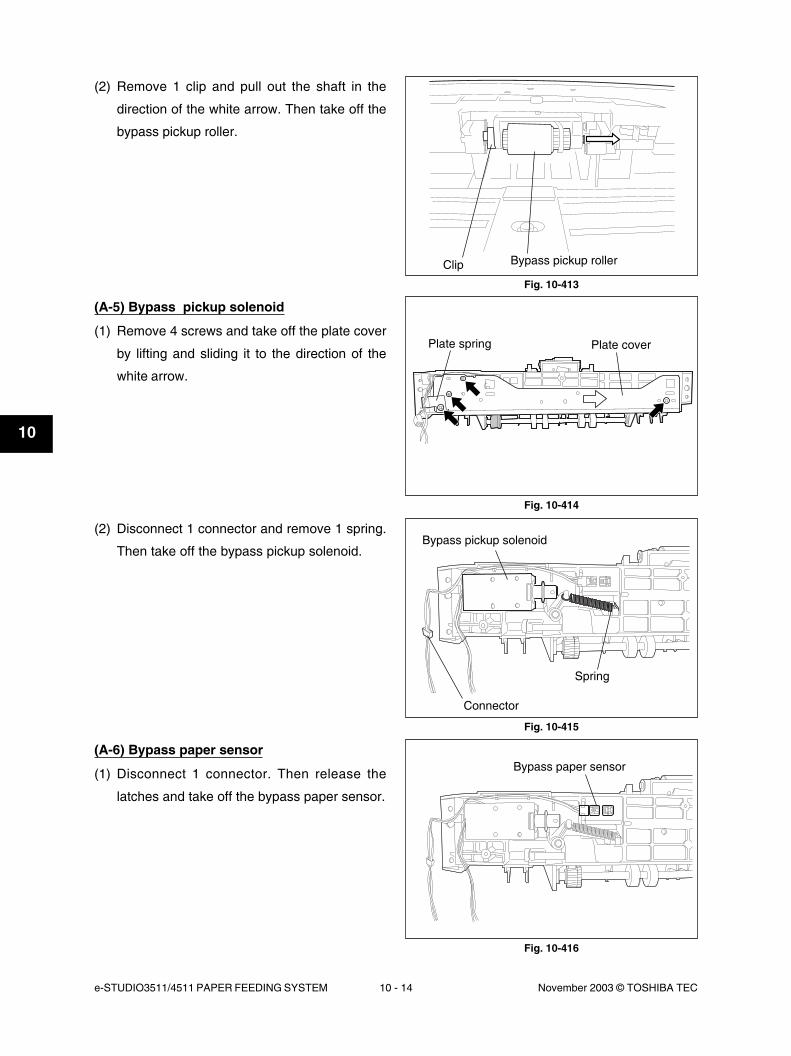
e-STUDIO3511/4511 PAPER FEEDING SYSTEM 10 - 14 November 2003 © TOSHIBA TEC
10
(A-6) Bypass paper sensor
(1) Disconnect 1 connector. Then release the
latches and take off the bypass paper sensor.
(2) Remove 1 clip and pull out the shaft in the
direction of the white arrow. Then take off the
bypass pickup roller.
(A-5) Bypass pickup solenoid
(1) Remove 4 screws and take off the plate cover
by lifting and sliding it to the direction of the
white arrow.
Clip Bypass pickup roller
Fig. 10-413
Fig. 10-414
(2) Disconnect 1 connector and remove 1 spring.
Then take off the bypass pickup solenoid.
Plate spring Plate cover
Fig. 10-415
Fig. 10-416
Bypass pickup solenoid
Connector
Spring
Bypass paper sensor

November 2003 © TOSHIBA TEC 10 - 15 e-STUDIO3511/4511 PAPER FEEDING SYSTEM
10
(A-7) Bypass feed roller
(1) Remove 4 screws and take off the bypass feed
unit.
(2) Remove 1 clip and take off the bypass feed
roller by sliding it.
Fig. 10-417
Fig. 10-418
Bypass feed unit
ClipBypass feed roller
(A-8) Bypass separation roller
(1) Remove 3 screws and take off the lower plate
cover.
Fig. 10-419
Fig. 10-420
Lower plate cover
Bypass separation roller(2) Take off the bypass separation roller.
Note: Lubricate the bypass separation roller on
every replacement. Refer to the Service
Handbook for more details.
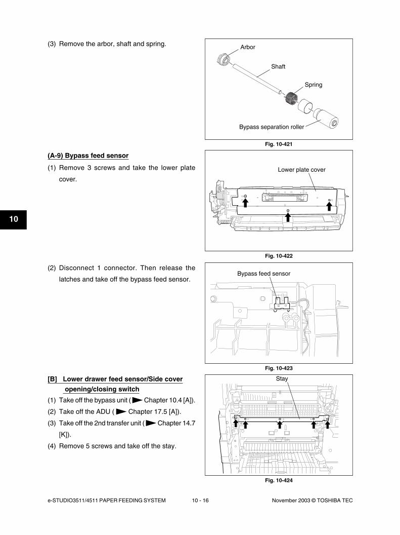
e-STUDIO3511/4511 PAPER FEEDING SYSTEM 10 - 16 November 2003 © TOSHIBA TEC
10
(2) Disconnect 1 connector. Then release the
latches and take off the bypass feed sensor.
Fig. 10-422
Fig. 10-423
Lower plate cover
Bypass feed sensor
Fig. 10-424
Stay
(3) Remove the arbor, shaft and spring.
Fig. 10-421
Arbor
Shaft
Spring
Bypass separation roller
[B] Lower drawer feed sensor/Side cover opening/closing switch
(1) Take off the bypass unit ( Chapter 10.4 [A]).
(2) Take off the ADU ( Chapter 17.5 [A]).
(3) Take off the 2nd transfer unit ( Chapter 14.7
[K]).
(4) Remove 5 screws and take off the stay.
(A-9) Bypass feed sensor
(1) Remove 3 screws and take the lower plate
cover.

November 2003 © TOSHIBA TEC 10 - 17 e-STUDIO3511/4511 PAPER FEEDING SYSTEM
10
Fig. 10-425
Fig. 10-426
Fig. 10-427
Guide
Lower drawer feedsensor
Side guide opening/closing switch
Clip
(2) Remove 3 screws. Rotate the guide to take it
off by releasing the harness from the harness
clamp.
Knob
Fig. 10-428
Guide
(5) Remove 3 screws and take off the guide by
sliding it to the rear side.
(6) Disconnect 1 connector and take off the lower
drawer feed sensor.
(7) Disconnect 1 connector and take off the side
cover opening/closing switch.
[C] Upper drawer feed sensor/Registration sensor
(1) Remove 1 clip and take off the knob.

e-STUDIO3511/4511 PAPER FEEDING SYSTEM 10 - 18 November 2003 © TOSHIBA TEC
10
Fig. 10-429
(3) Disconnect 1 connector and remove 1 screw.
Then take off the upper drawer feed sensor with
the whole bracket.
(4) Disconnect 1 connector and remove 1 screw.
Then take off the registration sensor with the
whole bracket.
Fig. 10-430
Fig. 10-431
Fig. 10-432
Upper drawer feed sensor
Registration sensor
Bracket
Registration roller(Metal roller)
Registration roller(Rubber roller)
Registration roller(rubber roller)
Registration roller(metal roller)
(6) Remove 1 clip, 1 bushing and 1 spring on each
front/rear side. Take off the registration roller
(metal roller) by sliding it to the rear side.
Note: The spring on the front side differs from the
one on the rear side. Note that the spring
on the rear side has a black marking. So
when installing, be careful not to mix them
up.
Spring(6)
Clip (6) Clip (5)
Spring (6)
Clip (6)Clip (5)
[D] Registration roller
(1) Take off the front right cover ( Chapter 2.5.1
[E]).
(2) Take off the transport motor drive unit (
Chapter 9.5 [B]).
(3) Remove 1 clip and take off the knob.
(4) Remove 1 screw and take off the bracket.
(5) Remove 1 clip and 1 bushing on each front/
rear side. Take off the registration roller (rubber
roller) by sliding it to the rear side.

November 2003 © TOSHIBA TEC 10 - 19 e-STUDIO3511/4511 PAPER FEEDING SYSTEM
10
Fig. 10-433
Fig. 10-434
Feed clutch
Note: Attach the clutch to the shaft referring to the
figure at right.
Fig. 10-435
0.2-0.5mm
(E-3) Separation roller
(1) Remove 1 screw and take off the separation
roller holder.
Fig. 10-436
Separation roller
[E] Drawer feeding unit
(E-1) Drawer feeding unit
(1) Remove the drawer.
(2) Remove 1 screw and take off the drawer
feeding unit while sliding it to the front side.
(E-2) Feed clutch
(1) Disconnect 1 connector.
(2) Remove 2 screws and take off the clutch
bracket.
(3) Loosen 1 setscrew.
(4) Remove the feed clutch.

e-STUDIO3511/4511 PAPER FEEDING SYSTEM 10 - 20 November 2003 © TOSHIBA TEC
10
(E-4) Pickup roller
(1) Take off the pickup roller from the pickup arm
and remove the belt.
Fig. 10-438
Fig. 10-439
Fig. 10-440
Fig. 10-437
LOCK
LOCK
Lever
CoverClutch spring
Separation roller
Shaft
HolderArbor
Spring
Arbor
Spring
CLUTCH-6-L
Paper
Feed roller
Pickup roller
Separation roller
One-way clutch
Belt
Pickup armPickup rollerPickup arm
(2) Remove the lever from the holder and take off
the separation roller along with its shaft.
(3) Take off the cover, arbor, clutch spring, and then
the separation roller from the shaft.
Note: When reassembling the pickup roller, feed
roller and separation roller, pay attention to
the followings:
1. Set the timing belt securely on the pulleys.
2. Pay attention to the "lock" direction of the
one-way clutch.
3. Fit the clips securely into the groove on
the shaft.
4. Confirm that there is no oil staining etc.
on the surface of the timing belt, pulleys
and rollers.
5. Pay attention to the mounting direction of
the rollers.
6. Lubricate the separation roller on every
replacement. Refer to the Service
Handbook for more details.

November 2003 © TOSHIBA TEC 10 - 21 e-STUDIO3511/4511 PAPER FEEDING SYSTEM
10
Fig. 10-442
Fig. 10-443
Clip Feed roller One-way clutch
Drawer tray-up sensor Latch
Drawer empty sensor
(E-5) Feed roller
(1) Remove the clip and take off the feed roller in
the direction of the arrow.
(E-6)Drawer tray-up sensor and Drawer empty
sensor
(1) Disconnect the connector and release the
latches, and then take off the drawer tray-up
sensor.
(2) Disconnect the connector and release the
latches, and then take off the drawer empty
sensor.
(2) Remove the pulley, one-way clutch and 3
E-rings.
Fig. 10-441
E-ring
PulleyOne-way clutch
Pickup roller
E-ring
(E-7) Drawer paper stock sensor
(1) Disconnect 1 connector.
(2) Release the latches and take off the drawer
paper stock sensor.
Fig. 10-444
Drawer paper stocksensor

e-STUDIO3511/4511 PAPER FEEDING SYSTEM 10 - 22 November 2003 © TOSHIBA TEC
10
(4) Turn the tray drive unit. Release 6 latches and
take off the cover.
Note: When taking off the cover, be careful of the
spring inside the tray drive unit which
pushes the cover.
(5) Take off the tray-up motor.
Note: When assembling the tray drive unit, match
the gear bosses with the holes of the cover.
Latch
Cover
Bosses
Tray-up motor
(3) Disconnect 1 connector, remove 4 screws and
take off the tray drive unit.
Fig. 10-445
Fig. 10-446
Fig. 10-447
Fig. 10-448
Bracket
Latch
Latch
Latch
[F] Tray drive unit
(1) Take off the fuse PC board bracket
Chapter 2.5.2 [H]).
(2) Remove 2 screws and take off the bracket.
Tray drive unit
04/05

November 2003 © TOSHIBA TEC 10 - 23 e-STUDIO3511/4511 PAPER FEEDING SYSTEM
10
(3) Remove 3 screws and 1 E-ring. Then take off
the clutch fixing bracket.
(4) Take off the lower transport clutch (low speed)
and the lower transport clutch (high speed).
Notes: 1. Do not push the transport roller shaft
strongly when installing the clutch fixing
bracket and tighten the screws in the
order of (a), (b) and (c). When the
installation is finished, open the side
cover and check if the transport roller
rotates smoothly.
2. Attach the clutch to the shaft referring to
the figure on the right.
Fig. 10-449
Fig. 10-450
(c)
(a)
(b)
Bracket
Bracket
E-ring
Lower transportclutch (Low speed)
Lower transportclutch (High speed)
[G] Lower transport clutch (Low/High speed)
(1) Take off the tray drive unit ( Chapter 10.4
[F]).
(2) Remove 4 screws and take off the bracket.
Fig. 10-451
Clutch
Shaft0-0.5mm
[H] Registration guide
(1) Pull out the registration guide by holding its tab
on the front side.
(2) Clean the paper dust removal brush attached
on the registration guide.
Note: When taking off the registration guide, pay
attention not to drop the removed paper
dust from the brush into the inside of the
equipment.Fig. 10-452
Registration guide
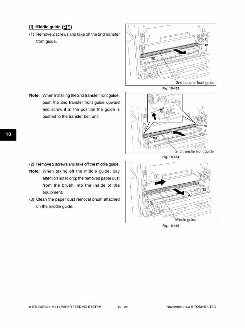
e-STUDIO3511/4511 PAPER FEEDING SYSTEM 10 - 24 November 2003 © TOSHIBA TEC
10
[I] Middle guide
(1) Remove 2 screws and take off the 2nd transfer
front guide.
Fig. 10-453
Fig. 10-454
Fig. 10-455
(2) Remove 2 screws and take off the middle guide.
Note: When taking off the middle guide, pay
attention not to drop the removed paper dust
from the brush into the inside of the
equipment.
(3) Clean the paper dust removal brush attached
on the middle guide.
Note: When installing the 2nd transfer front guide,
push the 2nd transfer front guide upward
and screw it at the position the guide is
pushed to the transfer belt unit.
2
1
2nd transfer front guide
2nd transfer front guide
Middle guide

November 2003 © TOSHIBA TEC 11 - 1 e-STUDIO3511/4511 DRUM RELATED SECTION
11
11. DRUM RELATED SECTION
11.1 ConstructionThis chapter explains about the drum, unit around the drum, image processing unit, their parts and
control circuits. This area mainly consists of the following components:
• Drum cleaner unit Drum
Main charger
Drum thermistor
Drum cleaner Cleaning blade
Toner recovery blade
Toner recovery auger
Drum cleaner brush
• Discharge LED unit Discharge LED
Ozone exhaust duct
Automatic wire cleaning drive unit
• Ozone exhaust fan
• Toner bag / Toner bag full detection sensors-1 & -2
(Toner volume detection sensor / toner pressure detection sensor)
• High-voltage transformer
• Image quality sensor ( Chapter 15)
• Temperature/Humidity sensor
Toner recovery blade
Drum cleaner brush
Toner recovery augerCleaning blade
Discharge LEDDrum
Toner bag full detection sensor-2
Toner bag full detection sensor-1
Fig. 11-101
Main charger
Drum thermistor Ozone exhaust duct
Automatic wire cleaning drive unit

e-STUDIO3511/4511 DRUM RELATED SECTION 11 - 2 November 2003 © TOSHIBA TEC
11
11.2 Functions(1) Drum
Drum is made of a cylindrical aluminum base coated with thin film of organic photoconductive sub-
stance.
Photoconductive object becomes insulative (high electrical resistance) when it is not exposed to
lights and becomes conductive (low electrical resistance) when it is exposed to lights. This object is
called photoconductor.
(2) Main charger
Main charger consists of a metal rod case having insulated blocks at the both ends with the charger
wire attached and the grid is set between them.
When high voltage is applied to the charger wire, the surrounding air is charged (ionized). Then a
flow of the ionized air into the drum applies the drum a charge as well. This phenomenon is called
“corona discharge” and a control bias is applied to the grid to control the charging amount. Negative
charge caused by the corona discharge is applied to the drum surface evenly in dark places. Charger
wire is equipped with an automatic wire cleaner to clean the wire.
(3) Drum thermistor
Since the photoconductive characteristic of the drum surface changes depending on the tempera-
ture of the drum surface, the drum thermistor detects the temperature of the drum surface and
controls to gain the charging potential according to the environment.
(4) Drum cleaner
(a) Cleaning blade
This blade is pressed against the drum surface with a constant force by pressure springs, and
scrapes off the residual toner on the drum surface. Also it removes the positive charge on the
photoconductive drum by applying negative charge on the blade.
(b) Recovery blade
This blade catches the toner scraped off by the cleaning blade.
(c) Toner recovery auger
This auger carries the residual toner scraped off to the toner bag.
(d) Drum cleaner brush
This brush roller prevents the residual toner and foreign matter adhering to the drum surface.

November 2003 © TOSHIBA TEC 11 - 3 e-STUDIO3511/4511 DRUM RELATED SECTION
11
(5) Discharge LED
Discharge is a process to decrease or eliminate the static electricity on the drum surface.
The electrical resistance of the photosensitive layer is decreased by the light, and the residual charge
on the drum surface is neutralized and eliminated (cleaned). Electrical potential of the drum surface
is fixed to a certain amount before the drum is charged.
(6) Toner bag
This collects the residual toner scraped off on the drum surface by the cleaning blade and residual
toner scraped off on the transfer belt by the transfer belt cleaning blade.
(7) Toner bag full detection sensors-1 & -2
The sensor-2 (transmissive type) finds the toner bag full by detecting the volume of used toner in the
toner bag. The sensor-1 detects the toner bag full when it is pushed by the toner recovery auger in
the cleaner which is given a pressure from the used toner in the toner bag.
The toner bag full detection sensor-2 also detects the presence/absence of the toner bag.
“Toner bag full” is determined when either of the toner bag full detection sensors-1 and -2 detects full
of toner. Printing is interrupted upon the detection of “Toner bag full” status, however, the paper
already fed is subject to be printed and exited. When the sensors are in trouble, “Toner bag full” is
determined instead of “Call for service”. If “Toner bag full” status is not cleared, the sensors, harnesses
and LGC board need to be checked.
(8) High-voltage transformer
A circuit generates the output control voltage Vc of the main charger bias, main charger grid bias, 1st
transfer roller bias, 2nd transfer roller bias, black developer bias, color developer bias and cleaning
blade bias.
(9) Image quality sensor
This sensor measures the reflection amount of the test pattern (toner image) formed on the transfer
belt and outputs to the LGC board in order to keep the appropriate image density and line width.
(10) Temperature/humidity sensor
This sensor measures the environment inside the equipment. The values of the temperature and
humidity detected inside the equipment are output to the LGC board.

e-STUDIO3511/4511 DRUM RELATED SECTION 11 - 4 November 2003 © TOSHIBA TEC
11
Fig. 11-301
11.3 Output Control Circuits of High-Voltage Transformer
• Outputs adjustment value of the main charger, transfer charger, and developer biases in the NVRAM
to the main processor.
↓
• Outputs control voltage data from the main processor to the D/A converter.
↓
• Analog conversion by the D/A converter.
↓
• Outputs control voltage Vc to the main charger grid bias, 1st transfer roller bias, 2nd transfer roller
bias, color developer bias and black developer bias transformer.
↓
• The main charger bias, 1st transfer roller bias, 2nd transfer roller bias, color developer bias and black
developer bias transformers generate output current or voltage proportional to the control voltage Vc
with the output ON signal.
* Adjustment of the control voltage Vc (change of adjustment data) is performed in the Adjustment
Mode (05).
* Output value of the cleaning blade bias is fixed when the transformer board is shipped from the
factory.
MAINCPU
NVRAM
Main charger grid
1st transfer
2nd transfer
Black developer
Color developer
Main charger ON
1st transfer
2nd transfer
Black developer (DC) ON
Black developer (AC) ON
Cleaning blade ON
Color developer (DC) ON
Color developer (AC) ON
D/Aconverter
IC8
Transistorarray
IC7
Gatearray
IC29
IC34

November 2003 © TOSHIBA TEC 11 - 5 e-STUDIO3511/4511 DRUM RELATED SECTION
11
11.4 Drum Temperature Detection Circuit(1) Purpose of the drum temperature detection circuit
Since the photoconductive characteristic of the drum surface varies drastically depending on the
surface temperature of the drum, this circuit detects the temperature of the drum surface to gain the
charging potential according to the environment.
(2) Configuration of the drum temperature detection circuit
Temperature/humidity sensor
Fig. 11-401
CPU
AN7
R8R7
R9
VTEMP
RTH

e-STUDIO3511/4511 DRUM RELATED SECTION 11 - 6 November 2003 © TOSHIBA TEC
11
11.5 Temperature/Humidity Sensor11.5.1 General description
This sensor measures the temperature and humidity inside the equipment.
11.5.2 Construction
Temperature/humidity control circuit is configured as follows:
Fig. 11-501
R TH
+-
+-
V HUMI
V TEMP
CPU
AN1
PB1
TEMP/HUMI
ANSW
MM
74H
C40
53
TEMP/HUMI-SNRLGC board

November 2003 © TOSHIBA TEC 11 - 7 e-STUDIO3511/4511 DRUM RELATED SECTION
11
11.6 Charger Wire Cleaner11.6.1 Operation
This equipment includes an automatic cleaning function with a motor drive to automatically clean off the
toner adhered on the main charger wire. The drive from charger wire cleaner motor is transmitted to the
wire cleaner through the timing belt and the wire cleaner contacted by the main charger wire shuttles
between the both ends of main charger wire. The waiting position (home position) of the wire cleaner is
at the front side. The wire cleaner and main charger wire are not contacted each other at the waiting
position.
The cleaning movement is performed in the cases as follows:
(1) When the power is turned ON
(2) When recovered from the energy saving mode
(3) When opening/closing the front cover
(4) When the specified number of pages has been printed out (default value: 1,000 pages) from the last
cleaning (If the number of pages has reached the setting value during continuous printing, the clean-
ing movement is performed upon the completion of this printing job.)
11.6.2 Construction
(1) Charger wire cleaner motor
This motor is a DC brush motor and supplies the drive to the wire cleaner. When the motor rotates in
reverse, the wire cleaner shifts to the rear side. Also when the motor rotates normally, the wire
cleaner shifts to the front side.
(2) Charger wire cleaner front position detection switch
This switch detects whether the wire cleaner has reached to the front position (home position) or not.
The wire cleaner is always waited at this position except during cleaning movement.
(3) Charger wire cleaner rear position detection switch
This switch detects whether the wire cleaner has reached to the rear position or not. When this
switch is turned ON, the charger wire cleaner motor rotates normally. Then the wire cleaner shifts to
the front position (home position).

e-STUDIO3511/4511 DRUM RELATED SECTION 11 - 8 November 2003 © TOSHIBA TEC
11
11.6.3 Drive circuit
The circuit configuration is as shown below.
Fig. 11-601
Signal level of motor circuit
Signal level of switching circuit
Signal
ENVMT1-0
Wire cleaner drive signal-1
ENVMT2-0
Wire cleaner drive signal-2
OFF
L
L
Reverse
rotation
L
H
Normal
rotation
H
L
Brake
H
H
Signal
ENVSNR1-0
Charger wire cleaner front
position detection signal
ENVSNR2-0
Charger wire cleaner rear
position detection signal
L
Charger wire cleaner is at the front
position
Charger wire cleaner is at the rear
position
H
Charger wire cleaner is at the
position other than the front
position
Charger wire cleaner is at the
position other than the rear
position
Motor
Level
LGC board PWA-CCL
CPU
Driver
ASICGA
ENVMT1-0
ENVMT2-0
ENVSNR1-0
ENVSNR2-0
M

November 2003 © TOSHIBA TEC 11 - 9 e-STUDIO3511/4511 DRUM RELATED SECTION
11
Fig. 11-701
Fig. 11-702
(5) Rotate the lever counterclockwise to screw it
again.
11.7 Disassembly and Replacement[A] Cleaner unit
(1) Open the front cover. Take off the toner bag
and black developer unit cover ( Chapter
2.5.1 [A], 12.8 (A-1)).
(2) Remove 1 screw and take off the sensor cover.
(3) Remove 3 screws.
(4) Loosen 2 screws.
Fig. 11-703
Fig. 11-704
Sensor cover
Lever

e-STUDIO3511/4511 DRUM RELATED SECTION 11 - 10 November 2003 © TOSHIBA TEC
11
(6) Disconnect 2 connectors. Remove 3 screws
and washer and pull out the cleaner unit.
Fig. 11-705
Washer
Cleaner unit
Notes: 1. When pulling out the drum cleaner unit,
pull out straightly without leaning.
2. When pulling out the drum cleaner, check
whether color developer is taking the
regular position (the position where color
toner cartridge can be pulled out from the
front) or not. If it is not taking the regular
position, rotate the revolver unit to the
regular position.
Fig. 11-706
4. If the transfer belt drive gear is not prop-
erly engaged, the hole positions of the
fixing screw (as shown in the figure at
right) may not match. In this case, oper-
ate the main motor for approx. 1 second
in the Test Mode (03-101) to engage the
drive gear securely and then install the
unit.
Fig. 11-707
3. If the transfer belt drive gear is not prop-
erly engaged, take off the receiving tray,
and then press the unit down until the
unit is securely fixed (as shown in the
figure at right) to engage the transfer belt
drive gear.
04/05

November 2003 © TOSHIBA TEC 11 - 11 e-STUDIO3511/4511 DRUM RELATED SECTION
11
(B-2) Main charger grid
(1) Push the terminal head at the front side and
remove the grid.
Note: Do not touch the mesh area of the grid.
Fig. 11-710
[B] Main charger unit
(B-1) Main charger unit
(1) Take off the cleaner unit ( Chapter 11.7 [A]).
(2) Rotate the gear counterclockwise for more than
1 turn.
(3) Release the latches and take off the main
charger unit.
Notes: 1. At this time, be careful not to touch the
drum surface or damage the drum.
2. When installing the main charger unit,
rotate the gear counterclockwise for
more than 1 turn until the holder arm is
completely hidden inside to install the
unit.
Fig. 11-708
Fig. 11-709
12
2
Gear
Main charger unit
Gear
Holder arm

e-STUDIO3511/4511 DRUM RELATED SECTION 11 - 12 November 2003 © TOSHIBA TEC
11
(2) Remove the terminal, detach the spring and
take off the wire.
Notes: Be careful of the followings when attaching
the wire.
1. Securely insert the wire into the V-
grooves of the front and rear sides.
2. Do not twist the wire.
3. Do not touch the wire directly with bare
hands.
(B-4) Wire pad
(1) Take off the charger wire ( Chapter 11.7
(B-3)).
Note: When installing, pay attention to the direction
of the wire pad.
(2) Release the latch and remove the wire pad.
Spring
Terminal
(B-3) Charger wire
* Length: 373 mm, tungsten wire diameter 0.06 mm
(1) Take off the terminal covers of the front and rear
sides.
Fig. 11-711
Fig. 11-712
Fig. 11-713
Wire
Latch
(3) Remove 1 screw and take off the pad guide.
Fig. 11-714
Pad guide

November 2003 © TOSHIBA TEC 11 - 13 e-STUDIO3511/4511 DRUM RELATED SECTION
11
(3) Take off the drum upward by sliding it toward
the front side.
Notes: 1. Do not touch, scratch or spit on the drum
surface.
2. Try to avoid direct sunlight to the drum.
Lay it on the dark place immediately after
taking off.
3. Do not touch the drum thermistor during
the disassembly and replacement.
4. Do not touch or damage the edge of the
cleaning blade.
5. When replacing the drum, take off the
drum shaft bearing from the old drum and
install it on the new drum.
6. Check the color deviation after replacing
the drum.
Fig. 11-717
Drum
[C] Drum
(1) Take off the cleaner unit ( Chapter 11.7 [A]).
(2) Remove 3 screws and take off the bracket.Bracket
Fig. 11-716
(4) Remove the base.
Note: Reinstall the base at the same position on
the belt as before removing. It is recommend-
able to leave the mark on the belt in advance.
Fig. 11-715
Base
Drum shaftbearing
04/10

e-STUDIO3511/4511 DRUM RELATED SECTION 11 - 14 November 2003 © TOSHIBA TEC
11
[D] Cleaner
(D-1) Drum cleaning blade
(1) Take off the main charger unit and drum.
( Chapter 11.7 (B-1) [C])
(2) Remove 3 screws and the cleaning blade.
Notes: 1. Do not touch or damage the edge of the
cleaning blade.
2. Check the color deviation after replacing
the drum cleaning blade. Fig. 11-718
Fig. 11-719
(D-2) Recovery blade
(1) Remove the recovery blade.
Notes: 1. To attach the recovery blade, clean the
surface of the frame beforehand to make
sure not to deform the blade.
2. Attach the recovery blade while pushing
it to the step on the surface of the frame.
3. Press the stuck part with your finger to
attach the blade securely.
Cleaning blade
Recovery blade
(D-3) Drum cleaner brush
(1) Unlock the lever by rotating it and pull it out.
Fig. 11-720
Lever
(2) Remove the drum cleaner brush.
Fig. 11-721
04/10

November 2003 © TOSHIBA TEC 11 - 15 e-STUDIO3511/4511 DRUM RELATED SECTION
11
Fig. 11-725
(3) Remove the discharge LED.
[F] Discharge LED unit
(F-1) Discharge LED
(1) Take off the black developer unit and cleaner
unit ( Chapters 12.8 [A] and 11.7 [A]).
(2) Remove 2 screws and lift up the discharge LED
unit. Disconnect 2 connectors, then take off the
discharge LED unit.
Fig. 11-724
(3) Remove 1 screw and take off the drum
thermistor.
Fig. 11-723
[E] Drum thermistor
(1) Take off the drum ( Chapter 11.7 [C]).
(2) Remove 1 screw and disconnect 1 connector,
and then take off the drum thermistor with the
whole bracket.
Fig. 11-722
Connector
Discharge LED unit
Discharge LED

e-STUDIO3511/4511 DRUM RELATED SECTION 11 - 16 November 2003 © TOSHIBA TEC
11
(F-2) Charger cleaner motor
(1) Take off the discharge LED unit ( Chapter
11.7 (F-1)).
(2) Disconnect the joint connector of the charger
cleaner motor.
(3) Remove 1 screw and take off the charger
cleaner motor unit.
(4) Remove 2 screws and take off the gear bracket
and motor guide.
(5) Remove 2 screws and take out the charger
cleaner motor from the motor bracket by
rotating it upward.
Fig. 11-726
Fig. 11-727
Fig. 11-728
Motor guide
Gear bracket
Fig. 11-729
(F-3) Charger cleaner detection switch
(1) Take off the charger cleaner motor unit (
Chapter 11.7 (F-2)).
(2) Separate the discharge LED unit into two parts.

November 2003 © TOSHIBA TEC 11 - 17 e-STUDIO3511/4511 DRUM RELATED SECTION
11
Fig. 11-732
[G] Toner bag full detection sensors
(G-1) Toner bag full detection sensor-1
(1) Take off the developer unit, cleaner unit and
transfer belt unit ( Chapters 12.8 [A], 11.7
[A] and 14.7 [A]).
(2) Remove 1 screw and disconnect 1 connector.
Take off the toner bag full detection sensor-1
with the whole bracket.
(G-2) Toner bag full detection sensor-2
(1) Open the front cover.
(2) Release 4 latches and take off the toner bag
full detection sensor-2.
Fig. 11-733
(5) Disconnect 2 connectors and take off the
charger cleaner front position detection switch
and charger cleaner rear position detection
switch.
(3) Release 2 latches and take off the front position
switch arm.
(4) Remove 1 screw and take off the rear position
switch arm.
Fig. 11-730
Fig. 11-731
Front positionswitch arm
Rear positionswitch arm
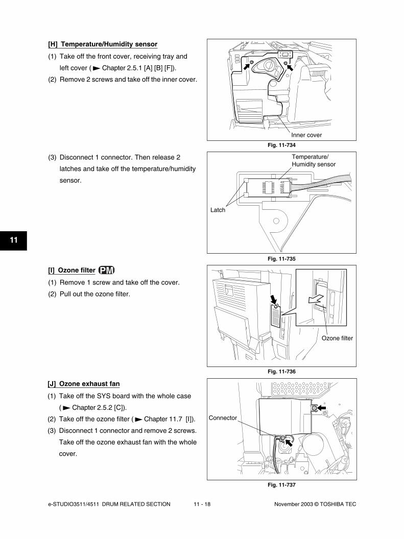
e-STUDIO3511/4511 DRUM RELATED SECTION 11 - 18 November 2003 © TOSHIBA TEC
11
[H] Temperature/Humidity sensor
(1) Take off the front cover, receiving tray and
left cover ( Chapter 2.5.1 [A] [B] [F]).
(2) Remove 2 screws and take off the inner cover.
Fig. 11-735
Fig. 11-736
[I] Ozone filter
(1) Remove 1 screw and take off the cover.
(2) Pull out the ozone filter.
(3) Disconnect 1 connector. Then release 2
latches and take off the temperature/humidity
sensor.
Fig. 11-734
Inner cover
Ozone filter
Latch
Fig. 11-737
[J] Ozone exhaust fan
(1) Take off the SYS board with the whole case
( Chapter 2.5.2 [C]).
(2) Take off the ozone filter ( Chapter 11.7 [I]).
(3) Disconnect 1 connector and remove 2 screws.
Take off the ozone exhaust fan with the whole
cover.
Connector
Temperature/Humidity sensor

November 2003 © TOSHIBA TEC 11 - 19 e-STUDIO3511/4511 DRUM RELATED SECTION
11
Fig. 11-738
Latch(4) Release 3 latches and take off the cover.
Take off the ozone exhaust fan.
FLO
W

e-STUDIO3511/4511 DRUM RELATED SECTION 11 - 20 November 2003 © TOSHIBA TEC
11

November 2003 © TOSHIBA TEC 12 - 1 e-STUDIO3511/4511 DEVELOPER UNIT
12
12. DEVELOPER UNIT
12.1 General Description
In this equipment, the three color developers (Y, M and C) are installed in the revolver unit and the black
developer is installed independently separated from the revolver unit. This special structure ensures the
improved printing productivity at the Black Mode. When developing color images (Y, M or C), the black
developer unit escapes contacting with the drum. When developing black images, each color developer
unit escapes from the drum by rotating the revolver and the black developer unit contacts with the drum
instead.
The developer motor drives the lifting movement and magnet roller rotation of the black developer unit,
and also the toner supply and magnet roller rotation of the color developer unit. Chapter 9 in this manual
describes more.
12.2 Construction• Black toner cartridge drive unit
• Developer motor drive unit Black developer unit Developer material
Mixer unit
Developer sleeve (magnetic roller)
Doctor blade
Black auto-toner sensor
Black developer unit lifting mechanism
Color developer unit Developer material
Mixer unit
Developer sleeve (magnetic roller)
Doctor blade
Color developer toner supply auger
• Color auto-toner sensor

e-STUDIO3511/4511 DEVELOPER UNIT 12 - 2 November 2003 © TOSHIBA TEC
12
12.3 Sectional View
Fig. 12-301
Color auto-toner sensor Mixer
Drum
Developer sleeve
MixerBlack developer unit
Black auto-toner sensor
Color developer unit
Developer sleeve

November 2003 © TOSHIBA TEC 12 - 3 e-STUDIO3511/4511 DEVELOPER UNIT
12
12.4 Black Toner Cartridge Drive Unit12.4.1 General descriptions
The black toner cartridge is filled with black toner, and supplies the toner to the black developer unit by
rotating the toner cartridge with the drive of the toner motor. The black toner cartridge detection switch
ensures that the black toner cartridge is in rotation by detecting the protrusion of the toner cartridge.
Also, the auto-toner sensor detects whether the toner cartridge is empty by detecting the toner density
ratio of the black developer unit.
12.4.2 Toner motor
The toner motor supplies toner to the black developer unit from the toner cartridge. It is driven by the
motor driver IC (TA8428K) through an overcurrent protection device. The overcurrent protection device
is mounted to protect the toner motor and toner motor driver. When the motor abnormality occurred and
the motor drive current exceeding the specified level surged, internal resistance of the overcurrent
protection device becomes high to cut off the current.
Its circuit configuration is shown below.
PE0
PE2
PB7
LCA301-2
KTNDET
KTNA1B
KTNA1A
TD
6238
5
TA84
28K
Gate array
Mot
or d
river
Toner motor
Fig. 12-401
Signal level for motor circuit
Signal State
KTNA1A-0 KTNA1B-0
L L OFF
Level L H CW (when supplying toner)
H L CCW (detecting cartridge installation)
H H Brake
Black tonercartridge
Overcurrentprotection
device

e-STUDIO3511/4511 DEVELOPER UNIT 12 - 4 November 2003 © TOSHIBA TEC
12
12.5 Black Developer Unit12.5.1 Functions
a. Black developer material
The developer material consists of the carrier and toner. The carrier is made of electrically con-
ductive ferrites which is 30-100 µm and the toner is made of the resin particle which is 5-20 µm.
Since the developer material deteriorates after a long time use, periodic replacements are needed.
b. Mixer unit
The carrier and toner are frictionized each other when the developer material is stirred. Then the
carrier is positively charged (+) and the toner is negatively charged (–), and the toner is adhered
by the electrostatic force.
c. Developer sleeve (Magnetic roller)
These aluminum rollers have magnets inside. The developer material is pulled by these magnets
to form a magnetic brush. The magnets are fixed at their position so only the sleeve rotates. By
this rotation, the developer material is transported to the developer sleeve. Then the magnetic
brush formed at the developer sleeve sweeps over the drum surface and thus development is
performed.
d. Doctor blade
The doctor blade controls the amount of the developer material from the transport sleeve so that
the magnetic brush of the developer material can contact with the drum surface properly.
e. Black auto-toner sensor
To print out a precise image, the proportion (toner density ratio) of the carrier and the toner in the
developer material needs to be always constant. The magnetic bridge circuit in the auto-toner
sensor detects the toner ratio in the developer material. This sensor supplies the toner from the
toner cartridge.

November 2003 © TOSHIBA TEC 12 - 5 e-STUDIO3511/4511 DEVELOPER UNIT
12
12.5.2 Black developer unit drive section
The black developer motor drives the black developer unit. Connection and disconnection of the devel-
oper motor drive is made by ON/OFF of the black developer drive clutch. The drive is connected when it
is ON and disconnected when it is OFF.
Fig. 12-501
Fig. 12-502
Developer sleeve
Doctor blade
Mixer-2Mixer-1
Gear (G19)
Gear (G20)
Gear (G21)
Gear (G20)
Gear (G19)

e-STUDIO3511/4511 DEVELOPER UNIT 12 - 6 November 2003 © TOSHIBA TEC
12
12.5.3 Black auto-toner sensor circuit
(1) Functions of auto-toner circuit
• Detection of the toner density in the developer material
- density lowered → toner supplied
• Detection of the toner being empty in the toner cartridge
CPUAN2
DICH1
LDCH1CLKCH1
PA1
LCA301-1
ATSDET
ATSVR
ATS74
07+-
+-
Black auto-toner
sensor
D/A
con
vert
er
Fig. 12-503

November 2003 © TOSHIBA TEC 12 - 7 e-STUDIO3511/4511 DEVELOPER UNIT
12
Magnetic resistance
Drivewinding
Detectionwinding
DCconversion
circuit
(Developer material)
Magnetic circuit
Auto-toner output
Main CPU(LGC board)VATS
Fig. 12-504
(2) Functions of the black auto-toner sensor
a. Initializing function: When unpacking and replacing the developer material
The automatic adjustment is made so that the output of the auto-toner sensor (input value of the
main CPU) will be 2.45V to 2.55V for the toner density of new developer material.
b. Toner density stabilizing function: During the printing operation
Through the following phases, the toner density is kept constant.
Toner is consumed.
→ Toner density decreases.
→ Output change of the auto-toner sensor is detected depending on the humidity.
→ Drives toner motor.
→ Supplies toner to the developer unit from the toner cartridge.
c. Toner-empty detection/clear function:
Detects toner being empty in the toner cartridge.
Drives toner motor.
→ Output of the auto-toner sensor is not changed.
→ Toner density is not changed.
→ Detects toner being empty.
Toner-empty clear
Drives toner motor.
→ Supplies toner from the toner cartridge.
→ Output of the auto-toner sensor changes.
→ Toner density recovers to its normal value.
→ “Toner-empty” is cleared.
(3) Operations of black auto-toner sensor
The black auto-toner sensor is composed of the following circuits.
Drive winding : Magnetic head (primary side) with a high-frequency magnetic field,
which forms a magnetic circuit in the developer material
Detection winding : Receiving the changes in the magnetic resistance of the developer
material via a magnetic circuit (secondary side)
DC conversion circuit : Converting the high-frequency output from the detection winding to a
DC signal

e-STUDIO3511/4511 DEVELOPER UNIT 12 - 8 November 2003 © TOSHIBA TEC
12
When the toner density is low:
Toner ratio to the carrier in the developer material decreases.
→ Magnetic resistance decreases.
→ Detection output increases.
→ Auto-toner output VATS increases.
When the toner density is high:
Toner ratio to the carrier in the developer material increases.
→ Magnetic resistance increases.
→ Detection output decreases.
→ Auto-toner output VATS decreases.
November 2003 © TOSHIBA TEC 12 - 9 e-STUDIO3511/4511 DEVELOPER UNIT
12
12.5.4 Black developer unit lifting mechanism
(1) General descriptions
In the black developer unit, the drive from the developer motor is transmitted to cam with the black
developer lifting clutch and this promotes the lifting movement of the black developer unit to contact
or release against the photoconductive drum. When developing color images, (Y, M or C), the black
developer unit escapes contact with the drum. When developing black images each color developer
unit releases from the drum by rotating its revolver and the black developer unit contacts with the
drum instead.
Black developer contact position detection sensor detects whether the black developer unit is at the
developing position or at the escape position.
(2) Construction
• Black developer lifting clutch
An electromagnetic clutch contacts or releases the black developer unit against the drum.
The clutch movement lifts the developer unit up and down by rotating the cam.
• Black developer contact position detection sensor
Detects whether the black developer unit is at the contact position or release position. This sensor
detects the shield plate. “L” is output when contacting and “H” is output when releasing.
• Black developer contact timing detection sensor
Controls the black developer lifting clutch. This sensor outputs reference timing signals for control-
ling ON/OFF of the black developer lifting clutch. “H” is output when releasing and “L” is output
when contacting. The sensor controls the power supply to turn OFF the clutch after detecting the
output alteration (“L” to “H” or “H” to “L”).

e-STUDIO3511/4511 DEVELOPER UNIT 12 - 10 November 2003 © TOSHIBA TEC
12
12.6 Color Developer Unit12.6.1 Functions
a. Color developer material
The developer material consists of the carrier and toner. The carrier is made of electrically conductive
ferrites which is 30-100 µm and the toner is made of the resin particle which is 5-20 µm. Since the
developer material deteriorates after a long time use, periodic replacements are needed.
b. Mixer unit
The carrier and toner are frictionized each other when the developer material is stirred. Then the
carrier is positively charged (+) and the toner is negatively charged (–), and the toner is adhered
by the electrostatic force.
c. Developer sleeve (Magnetic roller)
These aluminum rollers have magnets inside. The developer material is pulled by these magnets
to form a magnetic brush. The magnets are fixed at their position so only the sleeve rotates. By
this rotation, the developer material is transported to the developer sleeve. Then the magnetic
brush formed at the developer sleeve sweeps over the drum surface and thus development is
performed.
d. Doctor blade
The doctor blade controls the amount of the developer material from the transport sleeve so that
the magnetic brush of the developer material can contact with the drum surface properly.

November 2003 © TOSHIBA TEC 12 - 11 e-STUDIO3511/4511 DEVELOPER UNIT
12
12.6.2 Color developer unit drive section
The color developer motor drives the color developer unit. Connection and disconnection of the devel-
oper motor drive is made by ON/OFF of the color developer drive clutch. The drive is connected when it
is ON and disconnected when it is OFF. The transmitted drive operates the mixers.
Fig. 12-601
Fig. 12-602
Developer sleeve
Doctor blade
Mixer-F
Mixer-R
Coupling (G20)
Gear (G19)
Gear (G27)
Gear (G21)
Gear (G18)
Gear (G19/G27)

e-STUDIO3511/4511 DEVELOPER UNIT 12 - 12 November 2003 © TOSHIBA TEC
12
12.6.3 Color auto-toner sensor circuit
(1) General descriptions
The color auto-toner sensor detects the toner amount on the color developer sleeve with the reflec-
tion-type photosensor, differing from the black auto-toner sensor. Light-receiving elements of diffuse
reflection in this sensor detect the toner amount on the sleeves with the light amount reflected from
the sleeve surface. It detects the toner amount at the first forward position from the developing
position.
When the toner runs out, it supplies the toner from the toner cartridge with the color toner supply
auger driven by the color developer toner supply clutch.
Also, the color auto-toner sensor has a shutter which opens and closes by the solenoid. It prevents
stain to the sensor and calibrates the sensor with the reflection from the shutter.
BC-RAM
CPUGA
PWA-SYS
PWA-LGC
CPU
GA
LCA301
Driver
Driver OP-AMP
Control panel
Color toner cartridge sensor
Display
Color developer tonersupply clutch
Shutter solenoid
Color auto-toner sensor
Color developerunit
Color tonercartridge
Shutter drivingsignal
Toner densitysignal
D/A converter
Execution control unit
Fig. 12-603
Color developer toner supply clutchcontrol signal

November 2003 © TOSHIBA TEC 12 - 13 e-STUDIO3511/4511 DEVELOPER UNIT
12
(2) Functions of the color auto-toner sensor
a. Initializing function: When unpacking or replacing developer material
This sensor automatically adjusts the light amount of sensor to make the detected value of toner
density of new developer material by auto-toner sensor equal to the fixed value. Also, the de-
tected value by the reference plate is stored in memory after this adjustment.
b. Toner density stabilizing function:
The difference between the toner density on the sleeve and the toner density at the initialization
mentioned above is detected. Then the difference is adjusted to maintain the density at a certain
level.
The detected value of auto-toner sensor is corrected in comparison with the detected value by the
reference plate not to be affected with temperature, stain and deterioration.
Through the following phases, the toner density is kept constant.
Toner is consumed.
→ Toner density decreases.
→ Output change of the auto-toner sensor is detected at the preceding position to the developing
position.
→ Drives the developer motor at the developing position.
→ Drives the color developer toner supply clutch.
→ Supplies the toner for a specified period of time.
→ The same procedure is repeated for other two colors.
c. Toner-empty detection/clear function:
Detects toner being empty in the toner cartridge.
Drives toner motor.
→ Output of the auto-toner sensor is not changed.
→ Toner density is not changed.
→ Detects toner being empty (Toner-empty detection function).
Clears toner-empty.
Drives toner motor.
→ Supplies toner from the toner cartridge.
→ Output of the auto-toner sensor is changed.
→ Toner density recovers to its normal value.
→ “Toner-empty” is cleared. (Toner-empty clear function)
(3) Operations of the color auto-toner sensor
04/05

e-STUDIO3511/4511 DEVELOPER UNIT 12 - 14 November 2003 © TOSHIBA TEC
12
When the toner density is low:
Toner ratio to the carrier in the developer material decreases.
→ The light reflection amount decreases.
→ Detection output (voltage) decreases.
When the toner density is high:
Toner ratio to the carrier in the developer material increases.
→ The light reflection amount increases.
→ Detection output (voltage) increases.
12.6.4 Color toner supply
1. The color developer unit whose toner needs to be supplied moves to the developing position.
2. The developer unit is driven and the toner is supplied for a regulated period of time.
3. The drive is stopped and the unit moves to the color toner density detection position to detect the
density.
4. When the toner density detected is higher than the regulated value, it moves to the escape position.
When the toner density detected is lower than the regulated value, it repeats the procedure 1 to 3 for
five times. If the toner density is still lower than the regulated value, it is judged as “toner empty” and
the unit moves to the escape position.
5. Procedure 1 to 4 is repeated for other color developer units when the toner supply is needed.
November 2003 © TOSHIBA TEC 12 - 15 e-STUDIO3511/4511 DEVELOPER UNIT
12
12.7 High-Voltage Transformer Output Control CircuitDeveloper bias is supplied from high-voltage power supply to the developer sleeve and the toner image
on the developer sleeve is transferred onto the photoconductive drum.
A color developer bias and a black developer bias are output separately.
Each developer bias consists of DC and AC which has an independent ON/OFF control. At DC, D/A
converter adjusts the level of output value in both color and black modes since each mode has a different
control condition.
Fig. 12-701
• Outputs adjustment value of the developer bias (DC) in the NVRAM to the main processor.
↓
• Outputs control voltage data from the main CPU to the D/A converter.
↓
• Analog conversion by the D/A converter.
↓
• Outputs control voltage Vc to the developer bias transformer.
↓
• The developer bias transformer generates output voltage proportional to the control voltage Vc by ON-
signed.
* Adjustment of the control voltage Vc (change of adjustment data) is performed in the adjustment
mode.
CPU
LCA301-2
KDVDON-0
KVDAON-0
CDVDON-0
CDVAON-0
KDVVR
CDVVR
PW
A-H
VTGate array
Buf
fer
Black developersleeve
Photoconductivedrum
Color developer sleeve
D/Aconverter

e-STUDIO3511/4511 DEVELOPER UNIT 12 - 16 November 2003 © TOSHIBA TEC
12
12.8 Disassembly and Replacement[A] Black developer unit
(A-1) Black developer unit
(1) Open the front cover and take out the toner
bag ( Chapter 2.5.1 [A]).
(2) Turn the black developer unit lifting lever to the
position where a clock hand could be at 9
o’clock. Remove 2 screws and take off the black
developer unit cover.
(3) Disconnect 2 connectors and remove 1 screw.
Pull out the black developer unit.
(A-2) Developer material
(1) Take off the black developer unit ( Chapter
12.8 (A-1)).
(2) Remove 2 screws and take off the upper cover.
Fig. 12-801
Fig. 12-802
Fig. 12-803
Fig. 12-804
(3) Discharge the developer material.
Upper cover
Black developerunit cover
Black developerunit lifting lever
ConnectorBlack developer unit

November 2003 © TOSHIBA TEC 12 - 17 e-STUDIO3511/4511 DEVELOPER UNIT
12
(4) Pour the developer material.
Note: When installing the upper cover, make sure
the urethan seal is covered by the upper
cover.
(A-3) Auto-toner sensor
(1) Discharge the developer material ( Chapter
12.8 (A-2)).
(2) Disconnect 1 connector, remove 1 screw and
take off the auto-toner sensor.
(A-4) Doctor blade
(1) Discharge the developer material ( Chapter
12.8 (A-2)).
(2) Remove 2 screws and take off the right cover.
Urethan seal
Auto-toner sensor
Right cover
Fig. 12-805
Fig. 12-806
Fig. 12-807
Fig. 12-808
Upper cover

e-STUDIO3511/4511 DEVELOPER UNIT 12 - 18 November 2003 © TOSHIBA TEC
12
(3) Remove 2 screws and take off the doctor blade.
(A-5) Developer sleeve
(1) Discharge the developer material ( Chapter
12.8 (A-2)).
(2) Take off the right cover ( Chapter 12.8 (A-4)).
(3) Remove 3 screws. Disconnect 1 connector and
take off the front cover.
(4) Remove 1 screw and take off the polarity
adjustment plate.
Note: Before disassembling, record (mark if any)
the scale pointed by the polarity adjustment
lever. Then match the polarity adjustment
plate at the scale previously recorded when
reassembling.
(5) Remove 1 screw and take off the bracket.
(6) Remove 3 screws and take off the rear cover.
Doctor blade
Polarity adjustment plate
Fig. 12-809
Fig. 12-810
Fig. 12-811
Fig. 12-812
Front cover
Bracket
Rear cover

November 2003 © TOSHIBA TEC 12 - 19 e-STUDIO3511/4511 DEVELOPER UNIT
12
(7) Front side: Remove the following parts installed
on the shaft of the developer sleeve in order:
Bushing, collar, roller, bearing-1, E-ring,
bearing-2 and oil seal.
* Procedure for replacing an oil seal:
Page 12-23
(8) Rear side: Remove the following parts installed
on the shaft of the developer sleeve in order:
E-ring, bushing, collar, roller, bearing-1, E-ring,
gear, pin, bearing-2 and oil seal.
(9) Take off the developer sleeve.
* Procedure for replacing an oil seal:
Page 12-23
(A-6) Mixer
(1) Discharge the developer material ( Chapter
12.8 (A-2)).
(2) Take off the developer sleeve ( Chapter 12.8
(A-5)).
(3) Front side: Remove the following parts
installed on the shaft of each mixer in order:
E-ring, bushing-1 and bushing-2.
* Procedure for replacing an oil seal:
Page 12-23
(4) Rear side: Remove the following parts installed
on the shaft of each mixer in order: E-ring, gear,
bearing and oil seal.
* Procedure for replacing an oil seal:
Page 12-23
Fig. 12-813
Fig. 12-814
Fig. 12-815
Fig. 12-816
Developer sleeve
Bushing-2
E-ring
Bushing-1
E-ring
E-ring
Gear

e-STUDIO3511/4511 DEVELOPER UNIT 12 - 20 November 2003 © TOSHIBA TEC
12
(5) Take off the mixer from the hole of front side.
[B] Color developer unit
(B-1) Developer material
(1) Remove 2 screws, release 5 hooks and take
off the toner holder by rotating it.
Notes:
1. Do not try to release the hooks forcibly.
Mixer
Fig. 12-817
Fig. 12-818
2. When installing the toner holder, rotate
the holder with hooking the magnet roller
side of it.
3. When installing the toner holder, be care-
ful not to peel the seal.
Fig. 12-819
Fig. 12-820
04/01

November 2003 © TOSHIBA TEC 12 - 21 e-STUDIO3511/4511 DEVELOPER UNIT
12
(B-3) Developer sleeve
(1) Discharge the developer material ( Chapter
12.8 (B-1)).
(2) Remove the urethan seal ( Chapter 12.8 (B-2)).
(3) Front side: Remove 1 screw and take off the
polarity adjustment plate.
Note: Before disassembling, record (mark if any)
the scale pointed by the polarity adjustment
lever. Then match the polarity adjustment
plate at the scale previously recorded when
reassembling.
(B-2) Doctor blade
(1) Discharge the developer material ( Chapter
12.8 (B-1)).
(2) Remove the urethan seal.
(3) Remove 2 screws and take off the doctor blade.
Urethan seal
Polarityadjustment plate
Fig. 12-823
Fig. 12-824
Doctor blade
(2) Discharge the developer material.
(3) Pour the developer material.
Fig. 12-821
Fig. 12-822

e-STUDIO3511/4511 DEVELOPER UNIT 12 - 22 November 2003 © TOSHIBA TEC
12(6) Remove the following parts installed on the
shaft of the developer sleeve in order: E-ring,
bearing, gear, bearing and oil seal.
(7) Take off the developer sleeve.
* Procedure for replacing an oil seal:
Page 12-23
Fig. 12-827
Developer sleeve
(B-4) Mixer
(1) Discharge the developer material ( Chapter
12.8 (B-1)).
(2) Take off the developer sleeve ( Chapter 12.8
(B-3)).
(3) Front side: Remove the following parts in order:
E-ring, bushing-1 and bushing-2.
* Procedure for replacing an oil seal:
Page 12-23Fig. 12-828
Bushing-2
E-ring
Bushing-1
E-ring
(4) Remove the following parts installed on the
shaft of the developer sleeve in order: C-ring,
bearing-1, C-ring, E-ring, bearing-2 and oil seal.
* Procedure for replacing an oil seal:
Page 12-23
(5) Rear side: Remove 1 screw and take off the
gear assembly.Gear assembly
Fig. 12-825
Fig. 12-826

November 2003 © TOSHIBA TEC 12 - 23 e-STUDIO3511/4511 DEVELOPER UNIT
12<<Procedure for replacing an oil seal>>
1. Take off the oil seal by hooking out its inside
with a fine screwdriver and such.
2. Push in a new oil seal parallel to the frame,
bushing and so on with paying attention to its
direction (as shown by the figure at right).
3. Spread the grease (Alvania No.2; about 2-rice-
grain’s amount) all around the inside diameter.
Note: Wipe off the grease which has run off to the
inner side of the oil seal. Fig. 12-831
OutsideInside
Grease
Oil seal
(4) Rear side: Remove the following parts in order:
E-ring, gear, bearing or bushing, and oil seal.
* Procedure for replacing an oil seal:
Page 12-23
(5) Take off the mixer from the hole of front side.
Mixer
Fig. 12-829
Fig. 12-830
Gear
E-ring

e-STUDIO3511/4511 DEVELOPER UNIT 12 - 24 November 2003 © TOSHIBA TEC
12
Fig. 12-832
Spring
Spring
[C] Black developer lifting unit
(1) Take off the black developer toner supply unit
( Chapter 11.7 [K]).
(2) Remove the harnesses from 5 harness clamps.
Disconnect 3 connectors and remove 2 screws
and 2 springs. Take off the black developer
lifting unit.
Note: The springs on both front and rear sides differ
in the active coils (length of spring). When
installing, pay attention to its active coils
(length of spring).
Front side: 20 (longer)
Rear side: 18 (shorter)
(4) Remove 1 screw and disconnect 1 connector.
Then take off the black developer contact
position detection sensor with the whole
bracket.
Fig. 12-833
Fig. 12-834
Black developer contacttiming detection sensor
Black developer contactposition detection sensor
(3) Disconnect 1 connector and release the
latches. Then take off the black developer
contact timing detection sensor.

November 2003 © TOSHIBA TEC 12 - 25 e-STUDIO3511/4511 DEVELOPER UNIT
12
Fig. 18-835
Switchbracket
[D] Black toner supply unit
(1) Take off the laser optical unit ( Chapter 8.6
[A]).
(2) Take off the transfer belt unit ( Chapter 14.7
[A]).
(3) Take off the front cover ( Chapter 2.5.1 [A]).
(4) Take off the toner bag ( Chapter 2.5.1 [A]).
(5) Take off the black developer unit ( Chapter
12.8 [A]).
(6) Take off the cleaner unit ( Chapter 11.7 [A]).
(7) Take off the discharge LED unit ( Chapter
11.7 [F]).
(8) Take off the front lower cover ( Chapter 2.5.1
[D]).
(9) Take off the front right cover ( Chapter 2.5.1
[E]).
(10) Remove 2 screws and take off the bracket of
the front cover opening/closing switch. (It is
not necessary to disconnect the connectors.)
Fig. 12-837
Fig. 12-836
(12) Remove 2 screws and take off the cleaner
rail stay.
(11) Remove 1 screw and 1 clip, take off the transfer
belt contact lever. And then, take off the shaft.
Shaft Lever
Cleaner rail stay
Clip

e-STUDIO3511/4511 DEVELOPER UNIT 12 - 26 November 2003 © TOSHIBA TEC
12
Toner case
Harness
Fig. 12-838
Fig. 12-839
(13) Take off the black toner cartridge.
(14) Remove 2 screws, release the harness from
the hook and pull out the toner case by rotating
it a little.
(15) Remove 2 screws. Toner supply unit
Fig. 12-841
Fig. 12-840
Black tonercartridge switch
(17) Remove 1 screw and disconnect 1 connector
from the bracket. Then take off the black toner
cartridge switch with the whole bracket.
(16) Disconnect 2 connectors and take off the toner
supply unit by lifting up and pulling out toward
you to release it from the catch.
Connector
Hook
November 2003 © TOSHIBA TEC 12 - 27 e-STUDIO3511/4511 DEVELOPER UNIT
12
Fig. 12-842
Fig. 12-843
Toner motor
Cleaner rail stay
(18) Remove 2 screws and take off the toner motor.
[E] Black toner supply auger unit
(1) Take off the black toner supply unit ( Chapter
11.7 [K]).
(2) Take off the black developer lifting unit (
Chapter 12.8 [C]).
(3) Remove 1 screw and take off the cleaner rail
stay.
(4) Remove 2 screws and take off the black toner
supply auger unit.
Fig. 12-844
Black toner supplyauger unit

e-STUDIO3511/4511 DEVELOPER UNIT 12 - 28 November 2003 © TOSHIBA TEC
12

November 2003 © TOSHIBA TEC 13 - 1 e-STUDIO3511/4511 REVOLVER UNIT
13
13. REVOLVER UNIT
13.1 General DescriptionThe revolver unit has three colors (yellow, magenta and cyan) of developer units and three colors of
toner cartridges inside. The revolver rotates 120 degrees in a clockwise direction to move each color
developer unit to the developing position, and thus color development is performed. At black
development, the revolver rotates to move them to the escape position not to contact with the
photoconductive drum.
13.2 ConstructionThis chapter explains about the following units, parts and control circuits related to the revolver unit.
Refer to Chapter 12 for the color developer unit and Chapter 9 for the developer motor drive unit.
• Revolver motor
• Developer motor drive unit
• Color toner
• Color developer unit
• Color toner cartridge sensor
• Color auto-toner sensor
Color auto-toner sensor
[Revolver unit sectional view]
Fig. 13-201
Photoconductive drumRevolver homeposition sensor
Color tonercartridge sensor
Revolver unit
Revolver motor

e-STUDIO3511/4511 REVOLVER UNIT 13 - 2 November 2003 © TOSHIBA TEC
13
13.3 Functions(1) Revolver motor
The revolver unit rotates with the drive of the revolver motor (two-phase stepping motor). The revolver
home position sensor detects its home position.
(2) Developer motor drive unit
The developer motor drives the color developer unit and the toner supply auger in the revolver unit.
This drive is connected and disconnected by the color developer unit drive clutch and the color toner
supply clutch. Only the color developer unit at the developing position is driven by this motor.
(3) Color toner cartridge
The color toner cartridge and the color developer units are fitting each other to prevent misinstallation
of the color toner cartridge. Therefore, the revolver unit has no device preventing misinstallation.
(4) Color developer unit
The color developer units must be in the revolver unit to perform color development. Since the
revolver unit has no device to detect misinstallation, be careful not to install the wrong unit. Refer to
Chapter 12 for details.
(5) Color toner cartridge sensor
This sensor detects the installation fault of the color toner cartridge. It is an optical reflection sensor
detecting the installation fault with the reflecting light from the reflection section. The color toner
cartridge is detected at the toner cartridge replacement position.
(6) Revolver home position sensor
This sensor is a transmissive type light sensor detecting the revolver unit home position. The position
detection is performed at initialization. "Call for service" if it does not detect the position in a specified
period of time.

November 2003 © TOSHIBA TEC 13 - 3 e-STUDIO3511/4511 REVOLVER UNIT
13
13.4 Drive of Revolver UnitThe drive from the revolver motor is transmitted to the gear at the external layer of the revolver unit rear
side. Then the revolver unit rotates clockwise.
Revolver motor (G15)
Revolver unit (G135)
Revolver homeposition sensor
Fig. 13-401

e-STUDIO3511/4511 REVOLVER UNIT 13 - 4 November 2003 © TOSHIBA TEC
13
13.5 Revolver Motor Drive Circuit13.5.1 Revolver motorThe revolver motor (two-phase stepping motor) drives over the DRV board circuit.
SDK03MRVMA
RVMB
RVMC
PWA-F-LGC
Revolver Motor
RVMD
RVMA-0
RVMC-0
RVMB-0
RVMD-0
FET
PG00
PG02
PG01
PG03
CPU
PD1
PD3
PD2LCA301
PWA-DRV
SDK03M
24V
FET
FET
FET
2SK2466 x 4
Fig. 13-501

November 2003 © TOSHIBA TEC 13 - 5 e-STUDIO3511/4511 REVOLVER UNIT
13
13.6 Operation13.6.1 Home position detection
The revolver unit detects its home position at every warming-up after the power is turned ON or the front
cover is opened/closed since this unit is driven by the stepping motor. The home position is the point
where the revolver home position sensor detects the shielded part in the revolver unit.
13.6.2 Escape position movementThe color developer units (C, M and Y) are escaped from the developing position when developing black
image by rotating the revolver unit. This escaping movement is performed after every home position
detection. The escape position is where these color developer units are during warming-up. The movement
always starts from the escape position when printing starts.
13.6.3 During warming-up
The home position detection and escape position movement are performed consecutively during warming-
up. Then the revolver unit operations such as toner supply and image quality control are performed
according to the conditions of the equipment.
13.6.4 During printing
The revolver unit moves in order, as follows:
Escape position (black image development) → Cyan image developing position → Magenta image
developing position → Yellow image developing position → Escape position (printing completed)
In addition to the basic movement mentioned above, the revolver operations such as toner supply and
image quality control are performed according to the conditions of the equipment.
1. Image quality control is performed immediately before the printing operation according to the conditions
of the equipment.
2. The revolver unit stays at the escape position to perform the black image development.
3. The revolver unit moves to the cyan image developing position after the completion of black image
development.
4. The cyan developer unit is driven and performs developing. At the same time, the density of magenta
toner is detected and the detection result is stored in memory.
5. The revolver unit moves to the magenta image developing position after the completion of cyan
image development.
6. The magenta developer unit is driven and performs developing. At the same time, the density of
yellow toner is detected and the detection result is stored in memory.
7. The revolver unit moves to the yellow developing position after the completion of magenta image
development.
8. The yellow developer unit is driven and performs developing. At the same time, the density of cyan
toner is detected and the detection result is stored in memory.
9. The revolver unit moves to the escape position to perform black image development after the
completion of yellow image development.
10. If any of color toner is judged as the low density, the revolver unit supplies the toner.
11. Procedure 2 to 10 is repeated when printing more than 1 page.
12. Printing finishes. Image quality control is performed according to the conditions of the equipment.

e-STUDIO3511/4511 REVOLVER UNIT 13 - 6 November 2003 © TOSHIBA TEC
13
13.6.5 Color toner supply
1. The color developer unit whose toner needs to be supplied moves to the developing position.
2. The developer unit is driven and the toner is supplied for a regulated period of time.
3. The drive is stopped and the unit moves to the color toner density detection position to detect the
density.
4. When the toner density detected is higher than the regulated value, it moves to the escape position.
When the toner density detected is lower than the regulated value, it repeats the procedure 1 to 3 for
five times. If the toner density is still lower than the regulated value, it is judged as “toner empty” and
the unit moves to the escape position.
5. Procedure 1 to 4 is repeated for other color developer units when the toner supply is needed.
13.6.6 During image quality control
1. A black test pattern is formed on the transfer belt while the revolver unit is at the escape position.
2. The revolver unit moves to the cyan developing position after the completion of the black image
development and a cyan test pattern is formed.
3. It moves to the magenta developing position after the completion of the cyan image development
and a magenta test pattern is formed.
4. It moves to the yellow developing position after the completion of the magenta image development
and a yellow test pattern is formed.
5. It moves to the escape position after completion of the yellow image development.
6. The image quality sensor reads the image density of four colors and feedbacks to the image quality
control.
7. Procedure 1 to 7 is repeated for one to six times until the specified gradation characteristic and
image density are obtained.

November 2003 © TOSHIBA TEC 13 - 7 e-STUDIO3511/4511 REVOLVER UNIT
13
13.7 Disassembly and Replacement[A] Color toner cartridge
(1) Rotate the revolver to the toner cartridge
replacement position.
Note: Perform the Test Mode (03) on the control
panel.
Yellow toner cartridge moves to the
replacement position: 03-452
Magenta toner cartridge moves to the
replacement position: 03-453
Cyan toner cartridge moves to the
replacement position: 03-454
(2) Open the front cover. Take off the color toner
cartridge while pressing the knob.
Fig. 13-701
Fig. 13-702Lock lever
Holder
[B] Color developer unit
(1) Take off the color toner cartridge ( Chapter
13.7 [A]).
(2) Take off the left cover ( Chapter 2.5.1 [F]).
(3) Rotate the revolver to the color developer
replacement position.
a. When rotate the revolver manually,
a-1. Lift up the revolver lock lever.
a-2. Rotate the revolver in the direction of white
arrow until it is locked.
Note: Do not touch the sleeve with bare hands.
b. When rotate the revolver automatically,
Start up the Test Mode (03) and use the
following codes.
Yellow developer unit moves to the
replacement position: 03-455
Magenta developer unit moves to the
replacement position: 03-456
Cyan developer unit moves to the
replacement position: 03-457

e-STUDIO3511/4511 REVOLVER UNIT 13 - 8 November 2003 © TOSHIBA TEC
13
Fig. 13-705
[D] Color toner cartridge sensor
(1) Take off the receiving tray ( Chapter 2.5.1
[B]).
(2) Disconnect 1 connector and remove 1 screw
and take off the color toner cartridge sensor
with the whole bracket.
Color toner cartridgesensorConnector
(4) Loosen 2 screws on each holder and take off 2
holders.
(5) Pull out and take off the color developer unit. If
the other color developer units still need to be
replaced, repeat the procedure (3) to (5). When
rotate the revolver unit manually, push down
the revolver lock lever and rotate it a little in the
direction of white arrow, and then follow the
procedure “a”.
Note: When installing the color developer unit, pay
attention to the direction of the holder.
Fig. 13-703
[C] Revolver motor
(1) Take off the rear cover ( Chapter 2.5.1 [P]).
(2) Take off the LGC board with the whole case
( Chapter 2.5.2 [A]).
(3) Disconnect 1 connector and remove 4 screws
and take off the revolver motor with the whole
bracket.
Connector
Fig. 13-704
[FRONT][REAR] [FRONT][REAR]

November 2003 © TOSHIBA TEC 13 - 9 e-STUDIO3511/4511 REVOLVER UNIT
13
(3) Remove 1 screw and take off the color toner
cartridge sensor.
[E] Color auto-toner sensor / Color auto-toner
sensor shutter solenoid
(1) Take off the receiving tray ( Chapter 2.5.1
[B]).
(2) Disconnect 1 connector and remove 3 screws.
Then take off the color auto-toner sensor unit.
(3) Remove 2 screws, disconnect 1 connector and
take off the color auto-toner sensor shutter
solenoid.
Fig. 13-706
Fig. 13-707
Fig. 13-708
Connector
Color auto-tonersensor unit
Color auto-toner sensorshutter solenoid
Connector
(4) Remove 2 screws and 1 spring and take off
the stay.
Fig. 13-709
Stay
Spring

e-STUDIO3511/4511 REVOLVER UNIT 13 - 10 November 2003 © TOSHIBA TEC
13
(5) Remove 1 E-ring and shaft and take off the color
auto-toner sensor case.
(6) Remove 2 screws and take off the color auto-
toner sensor.
Fig. 13-710
Fig. 13-711
Shaft
E-ringColor auto-tonersensor case
Color auto-tonersensor
[F] Revolver home position sensor
(1) Disconnect 1 connector and remove 1 screw.
Then take off the revolver home position sensor
with the whole bracket.
Fig. 13-712
Revolver homeposition sensor
[G] Color developer unit drive gear / Color
toner supply drive gear
(1) Take off the color developer unit ( Chapter
13.7 [B]).
(2) Release 2 latches and take off the holder. Then
take off the color developer unit drive gear and
color toner supply drive gear.
Fig. 13-713

November 2003 © TOSHIBA TEC 13 - 11 e-STUDIO3511/4511 REVOLVER UNIT
13
Fig. 13-715
Inner cover
[H] Revolver unit
(1) Take off all of the color developer units (
Chapter 13.7 [B]).
(2) Take off the cleaner unit ( Chapter 11.7 [A]).
Note: When taking off the cleaner, make sure that
all the color developer units are taken off in
advance. Otherwise the drum surface may
be scratched depending on the position of
the revolver unit (e.g. developing position).
(3) Take off the receiving tray ( Chapter 2.5.1
[B]).
(4) Take off the left rear cover ( Chapter 2.5.1
[G]).
(5) Take off the color toner cartridge sensor (
Chapter 13.7 [D]).
(6) Take off the color auto-toner sensor (
Chapter 13.7 [E]).
(7) Take off the internal cooling fan ( Chapter
13.7 [I]).
(8) Take off the laser optical unit ( Chapter 8.6
[A]).
(9) Release 2 latches take off the laser cooling duct
cover (rear side).
(10) Take off the revolver home position sensor
( Chapter 13.7 [F]).
(11) Remove 2 screws and take off the inner cover.
Notes: 1. When installing, insert the shaft of the
holder into the revolver unit securely.
2. Apply the grease to the shaft after the
replacement of the gears.
Fig. 13-714
Grease
Grease

e-STUDIO3511/4511 REVOLVER UNIT 13 - 12 November 2003 © TOSHIBA TEC
13
Fig. 13-718
Stay
Fig. 13-717
Lock lever
Fig. 13-716
(12) Remove 2 screws and take off the laser cooling
duct cover (front side).
(13) Take off the developer motor drive unit (
Chapter 9.5 [A]).
(14) Remove 1 screw and take off the lock lever.
(15) Remove 5 screws and the stay. (Remove 1 of
5 screws from the rear side of the equipment.)

November 2003 © TOSHIBA TEC 13 - 13 e-STUDIO3511/4511 REVOLVER UNIT
13
Fig. 13-720
(19) Slide the revolver to the front and take off the
bearing attached on the rear side of revolver
rotary shaft from the rear frame. Take off the
revolver unit with the bearing.
Fig. 13-721
Fig. 13-719
Bracket
(16) Remove 5 screws and take off the bracket.
(17) Remove the stopper attached on the front side
of the revolver rotary shaft.
(18) Push in the bearing to the inside of the frame
and take it off from the frame.
Note: Do not unscrew the red painted screws
(6 pcs.) on the revolver unit after taking off
the revolver unit.
Fig. 13-722

e-STUDIO3511/4511 REVOLVER UNIT 13 - 14 November 2003 © TOSHIBA TEC
13
Fig. 13-724
(3) Disconnect 1 connector and remove 2 screws.
Then take off the internal cooling fan.
[I] Internal cooling fan
(1) Take off the receiving tray ( Chapter 2.5.1
[B]).
(2) Disconnect 1 connector and remove 2 screws.
Then take off the internal cooling fan together
with the duct.
Fig. 13-723

November 2003 © TOSHIBA TEC 14 - 1 e-STUDIO3511/4511 TRANSFER UNIT
14
14. TRANSFER UNIT
14.1 General DescriptionsThe transfer unit transfers the toner image formed on the photoconductive drum to the transfer belt, and
then transfers it to the paper. The transfer of the toner image from the photoconductive drum to the
transfer belt is called 1st transfer and the transfer from the transfer belt to the paper is called 2nd transfer.
To reproduce a color image, maximum four color images are overlaid on the transfer belt and the overlaid
image is then transferred to the paper. Namely, the transfer belt turns four times for printing of one image.
The transfer belt rotates with the main motor drive.
14.2 Construction
Fig. 14-201
Transfer belt homeposition sensor-2
1st transfer roller
Drive roller-2
Transfer belt
Drive roller-1
2nd transfer roller
Transfer belt homeposition sensor-1
Idling roller
Drum
Transfer beltcleaning blade
Used tonerauger
Tension roller
2nd transfer roller positiondetection sensor

e-STUDIO3511/4511 TRANSFER UNIT 14 - 2 November 2003 © TOSHIBA TEC
14
14.3 Functions
(1) Transfer belt
The transfer belt is made by forming resin which has an electrical resistance with high precision.
The main motor drive rotates the transfer belt drive roller and that makes to rotate the transfer
belt as well.
(2) 1st transfer roller
When the 1st transfer bias from high-voltage power supply is applied, the toner is transferred
from photoconductive drum to the transfer belt. The spring presses to contact the transfer belt
with the photoconductive drum.
(3) Transfer belt cleaning blade
Removes the residual toner, paper dust or foreign objects on the transfer belt surface. Transfer
belt contact clutch performs contact/release movement.
(4) Transfer belt cleaner contact clutch
Performs contact/release movement between the transfer cleaning blade and transfer belt.
(5) Used toner auger
Transports the scraped residual toner and paper dust to the toner bag. The transfer belt cleaner
auger motor drives this auger.
(6) Drive roller-1
Rotates the transfer belt. This roller is driven by the transmitted drive from the main motor.
(7) Tension roller
Applies the tensile force to the transfer belt with its spring.
(8) Idling roller
Retains the contacting position of the transfer belt and the photoconductive drum.
(9) Drive roller-2
Contacts the transfer belt cleaning blade to the transfer belt easily. Also retains the contacting
position of the transfer belt and the photoconductive drum.
(10) Transfer belt home position sensor-1 and 2
Detects the home position of transfer belt. This reflection type sensor detects the reflection tape
inside of the transfer belt.
(11) 2nd transfer roller
When the 2nd transfer bias from high-voltage power supply is applied, the toner is transferred
from the transfer belt to the paper.
November 2003 © TOSHIBA TEC 14 - 3 e-STUDIO3511/4511 TRANSFER UNIT
14
(12) 2nd transfer roller contact clutch
This clutch is an electromagnetic clutch which contacts or releases the 2nd transfer roller to the
transfer belt. The 2nd transfer roller contacts when this clutch turns ON and releases when it
turns OFF. Since the transport motor is its drive source, the clutch needs to be ON as long as
they are contacting.
It also controls the clutch not to turn more than 180 degrees by the spring and stopper.
(13) 2nd transfer roller cleaning brush
When the toner is remaining on the 2nd transfer roller, it may stain the rear side of the paper.
This brush cleanses the 2nd transfer roller to prevent stain. In addition, the 2nd transfer section
needs a periodical cleaning since this section has no mechanism discharging scraped toner.
(14) 2nd transfer roller position detection sensor
This sensor is a photointerrupter detecting whether the 2nd transfer roller is at its contacting
position or releasing position.
(15) Paper clinging detection sensor
When the thin paper which is out of specification passes through, the thin paper may cling to the
transfer belt surface. In this case, the paper clinging to the belt cannot be removed in a usual jam
processing and thus a service call occurs. To prevent this, the sensor detects whether the thin
paper is clinging to the transfer belt or not, and processes this case as a paper jam.
04/05

e-STUDIO3511/4511 TRANSFER UNIT 14 - 4 November 2003 © TOSHIBA TEC
14
14.4 Outline of 1st transfer(1) The transfer belt contacts with the photoconductive drum. Power voltage is applied through the 1st
transfer roller and it transfers the toner onto the transfer belt.
(2) The transfer belt home position sensor-2 detects its home position and overlays four color images.
(3) When the transfer of the toner image from the transfer belt to the paper is completed in 2nd transfer,
residual toner on the transfer belt is scraped off by the transfer belt cleaning blade.
14.5 Outline of 2nd transfer(1) The 2nd transfer roller stays at the released position from the transfer belt in 1st transfer.
(2) Upon the completion of 1st transfer, the 2nd transfer roller starts to rotate and moves to the transfer
position.
(3) After an electrode bias is applied on the 2nd transfer roller, the toner image is transferred from the
transfer belt to the paper.
(4) Upon the completion of 2nd transfer, the 2nd transfer roller escapes to the releasing position.

November 2003 © TOSHIBA TEC 14 - 5 e-STUDIO3511/4511 TRANSFER UNIT
14
14.6 High-Voltage Power SupplyHigh-voltage power supply outputs the voltage of positive/negative polarity.
When the voltage of positive polarity is supplied to the 2nd transfer roller, the toner will be supplied from
the intermediary belt to the paper.
When the voltage of negative polarity is supplied to the 2nd transfer roller, the toner on the 2nd transfer
roller is transferred to the transfer belt reversely. The toner on the transfer belt is eliminated by the
cleaning unit and thus cleaning of the 2nd transfer roller is performed.
CPU
LCA-301-1
DVDON-0
DVAON-0B
UF
FE
R
PW
A-H
VT
+1000V, -1000V
2nd transfer roller
D/A
con
vert
er
Fig. 14-601
e-STUDIO3511/4511 TRANSFER/TRANSPORT UNIT 14 - 6 November 2003 © TOSHIBA TEC
14
Fig. 14-701
Fig. 14-702
Fig. 14-703
14.7 Disassembly and Replacement[A] Transfer belt unit
Note: Wearing gloves is recommended to avoid
direct touch by bare hands to the transfer
belt surface.
(1) Take off the drum cleaner unit ( Chapter 11.7
[A]).
(2) Take off the receiving tray ( Chapter 2.5.1
[B]).
(3) Take off the tray back cover ( Chapter 2.5.1
[C]).
(4) Unlock the fixing lever on the rear side by
rotating it.
(5) Unlock the fixing lever on the front side by
sliding it.
(6) Remove 1 screw and take off the fixing lever
on the front side.
1
2
1
2
(7) Disconnect 3 connectors.
Note: Make sure to connect each connector to the
socket in the same color as that of the
connector.

November 2003 © TOSHIBA TEC 14 - 7 e-STUDIO3511/4511 TRANSFER/TRANSPORT UNIT
14
Fig. 14-705
Fig. 14-706
Fig. 14-704
(8) Loosen 3 screws and take off the bracket.
(9) Lift up the transfer belt cleaning unit and move
it out to the front side temporarily. Then place
the unit on the rear frame and front frame.
(10) Pull out the transfer belt unit.
Notes: 1. When installing or taking off the transfer
belt unit, be careful not to scratch the
transfer belt.
2. Do not touch the transfer belt surface with
bare hands.
Transfer belt cleaning unit
Transfer belt unit
Bracket
3. When the transfer belt unit has been
installed or contact/release operation of
the unit has been performed, press the
unit down until the unit is securely fixed
(as shown in the figure at right) to engage
the transfer belt drive gear.
Fig. 14-707
04/05
e-STUDIO3511/4511 TRANSFER/TRANSPORT UNIT 14 - 8 November 2003 © TOSHIBA TEC
14
(3) Remove 1 screw and 2 stand plates.
Fig. 14-710
Stand plate (long)
Stand plate(short)
Fig. 14-709
[B] Transfer belt
Note: Wearing gloves is recommended to avoid
direct touch by bare hands to the transfer
belt surface.
(1) Take off the transfer belt unit ( Chapter 14.7
[A]).
(2) Remove 2 clips and take off the shaft by sliding
it to the rear side.
Note: When installing the shaft, insert the narrow
part of the shaft into the stay on the rear side
and fit it into the front side by sliding it.
4. If the transfer belt drive gear is not
properly engaged, the hole positions of
the fixing screw (as shown in the figure
at right) may not match. In this case,
operate the main motor for approx. 1
second in the Test Mode (03-101) to
engage the drive gear securely and then
install the unit.
Fig. 14-708
04/05

November 2003 © TOSHIBA TEC 14 - 9 e-STUDIO3511/4511 TRANSFER/TRANSPORT UNIT
14
Fig. 14-711
Fig. 14-712
Fig. 14-713
Stand plate (short)
Stay
(4) Remove 2 screws and take off the bracket.
(5) Install the stand plate (short) on the rear side
of the transfer belt unit using the screw which
is removed in step (3).
(6) Stand the transfer belt unit with its rear side on
the bottom.
(7) Remove 3 screws and the stay.
(8) Install the stand plate (long) on the front side of
the transfer belt unit using the screw which is
removed in step (7).
Fig. 14-714
Stand plate (long)

e-STUDIO3511/4511 TRANSFER/TRANSPORT UNIT 14 - 10 November 2003 © TOSHIBA TEC
14
2
1
1
Fig. 14-715
Fig. 14-716
Fig. 14-717
Shaft
Stay
Transfer belt
(9) Stand the transfer belt unit with its front side on
the bottom.
(10) Remove 3 screws.
(11) Incline the transfer belt unit so that the shaft
is pulled in the unit. Then remove the stay
while the shaft is hidden in the unit.
(12) Narrow the distance of rollers and pull out the
transfer belt unit.
Notes: 1. When installing the transfer belt, make
sure it is set at the center not to be moved
aside.
2. Make sure that the reflection tape inside
of the belt is on the rear side.
3. Do not touch the transfer belt surface with
bare hands.
4. Be careful not to scratch the transfer belt.
5. Check the color deviation after replacing
the transfer belt.
6. When replacing the transfer belt, remove
the oil from drive roller-1, drive roller-2,
tension roller, with a solvent such as
alcohol first, and attach the transfer belt.
[C] 1st transfer roller
(1) Take off the transfer belt ( Chapter 14.7 [B]).
(2) Remove 1 screw and the plate spring.
(3) Remove 1 screw and take off the bracket. Then
take off the 1st transfer roller and idling roller.
12
1st transfer roller Idling roller
Plate spring
Bracket
04/10

November 2003 © TOSHIBA TEC 14 - 11 e-STUDIO3511/4511 TRANSFER/TRANSPORT UNIT
14
Fig. 14-719
Fig. 14-720
Fig. 14-718
Fig. 14-721
Cover
Cover
[D] Transfer belt home position sensor-1
(1) Take off the transfer belt ( Chapter 14.7 [B]).
(2) Remove 1 screw and take off the cover.
(3) Remove 1 screw and disconnect 1 connector.
Then take off the transfer belt home position
sensor-1.
[E] Transfer belt home position sensor-2
(1) Take off the transfer belt ( Chapter 14.7 [B]).
(2) Remove 1 screw and take off the cover.
(3) Remove 1 screw and disconnect 1 connector.
Then take off the transfer belt home position
sensor-2.
Connector
Transfer belt homeposition sensor-1
ConnectorTransfer belt homeposition sensor-2

e-STUDIO3511/4511 TRANSFER/TRANSPORT UNIT 14 - 12 November 2003 © TOSHIBA TEC
14
Fig. 14-724
Cover(3) Release 2 latches and take off the cover.
Fig. 14-722
Fig. 14-723
[F] Transfer belt cleaning unit
(1) Take off the drum cleaner unit ( Chapter
11.6 [A]).
Note: When installing the transfer belt cleaning
unit, make sure to take off the drum cleaner
unit in advance since it may scratch the
drum.
(2) Take off the transfer belt unit ( Chapter 14.7
[A]).
(3) Disconnect 2 connectors and take off the
transfer belt cleaning unit.
Note: Do not incline the transfer belt cleaning unit
steeply since the toner may fall off.
Transfer belt cleaning unit
[G] Transfer belt cleaning blade / Blade seal
(1) Take off the transfer belt cleaning unit
( Chapter 14.7 [F]).
(2) Remove 2 blade seals on both ends of the
transfer belt cleaning blade.
Notes:1. When putting the blade seal, push the
seal firmly in the directions of the arrows
in the figure at right. Make sure that there
is no gap between the blade and seal.
2. Do not mix up the blade seal for front side
and one for rear side since they differ
each other.
Blade seal
04/10
November 2003 © TOSHIBA TEC 14 - 13 e-STUDIO3511/4511 TRANSFER/TRANSPORT UNIT
14
Fig. 14-726
Fig. 14-727
Fig. 14-725
Bracket(4) Remove 1 screw and take off the bracket on
the front side.
(5) Remove 1 screw and take off the bracket on
the rear side.
(6) Remove 2 springs.
Note: When installing the transfer belt cleaning
unit, after it’s completion, make sure the
springs do not come off.
Bracket
04/10
Fig. 14-728
(7) Separate the transfer belt cleaning unit into 2
parts.

e-STUDIO3511/4511 TRANSFER/TRANSPORT UNIT 14 - 14 November 2003 © TOSHIBA TEC
14
Fig. 14-732
[H] Transfer belt cleaner auger motor /
Transfer belt cleaner clutch
(1) Take off the transfer belt cleaning unit
( Chapter 14.7 [F]).
(2) Separate the transfer belt cleaning unit into
2 parts.
( Chapter 14.7 [G]).
(3) Release the latch and take off the gear.
Gear
Fig. 14-729
(8) Remove 3 conductive tapes.
Fig. 14-730
Note: When assembling, use the new conductive
tape. Also, attach the conductive tape to the
transfer belt cleaning blade referring to the
figure on the right.
Fig. 14-731
Cleaning blade
(9) Remove 2 screws and take off the transfer belt
cleaning blade.
Notes: 1. Make sure not to touch or damage the
edge of the blade.
2. Check the color deviation after replacing
the transfer belt cleaning blade.
04/10
Conductive tape
47 mm 160 mm
41 mm

November 2003 © TOSHIBA TEC 14 - 15 e-STUDIO3511/4511 TRANSFER/TRANSPORT UNIT
14
Fig. 14-733
Fig. 14-734
(4) Remove the harness clamp. Remove 1 screw
and take off the transfer belt cleaner auger
motor with the whole bracket.
(5) Remove 2 screws and take off the transfer belt
cleaner auger motor from the bracket.
Harness clamp
Transfer belt cleanerauger motor
Fig. 14-735
Fig. 14-736
(6) Remove 1 clip and take off 1 bushing. Then
take off the assembly of the shaft and clutch.
(7) Remove 1 clip. Remove 1 E-ring and take off
the bushing-1, and then take off the bushing-
2 with the shaft. Take off the transfer belt
cleaner clutch.
Shaft
Clutch
Bushing-2 Transfer beltcleaner clutch
Bushing-1
E-ring
Clip
04/10

e-STUDIO3511/4511 TRANSFER/TRANSPORT UNIT 14 - 16 November 2003 © TOSHIBA TEC
14
Fig. 14-739
Fig. 14-740
(4) Remove each part from the 2nd transfer
roller in order.
Notes:1. When assembling, pay attention to the
direction of the collar-2.
2. After assembling, check if the bushing-1,
bearing and collar-2 slide smoothly along
the axis of the shaft.
[J] 2nd transfer unit
(1) Take off the ADU ( Chapter 17.5 [A]).
(2) Take off the bypass unit ( Chapter 10.4 [A]).
(3) Take off the right rear cover
( Chapter 2.5.1 [L]).
(4) Remove 2 clips and 1 spring, and then take off
the slide hinge on the front side.
Collar-1Spring
Bushing-2
Collor-3
Slide hinge
Spring
Clip
Fig. 14-737
Fig. 14-738
[I] 2nd transfer roller
(1) Open the 2nd transfer unit.
(2) Release 4 latches and take off the cover.
(3) Remove 1 clip. Take off the 2nd transfer roller
while pushing the shaft.
Cover
Clip
2nd transferroller
04/10
Clip
Collar-1
Bearing
Bearing
Bushing-1
Collor-2Washer
Washer
November 2003 © TOSHIBA TEC 14 - 17 e-STUDIO3511/4511 TRANSFER/TRANSPORT UNIT
14
Fig. 14-741
Fig. 14-742
(5) Open the 2nd transfer unit. Disconnect 2
connectors, then remove 1 screw and the
ground wire. Remove 1 harness clamp.
(6) Take off the 2nd transfer unit.
Ground wire
Connector
Harness clamp
2nd transfer unit
Fig. 14-744
Fig. 14-743
[K] 2nd transfer roller contact clutch
(1) Take off the 2nd transfer unit
( Chapter 14.7 [J]).
(2) Take off the 2nd transfer roller
( Chapter 14.7 [I]).
(3) Remove 4 screws. Remove 1 screw and 2
ground wires, and then take off the transfer
guide.
(4) Remove 2 tension springs.
(5) Remove 2 clips.
(6) Take off the bushing-1 and slide the bushing-2.
Transfer guide
Ground wire
Bushing-2
Bushing-1
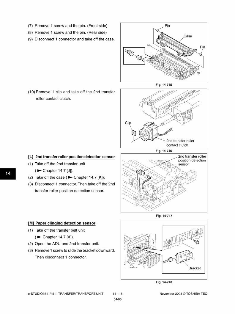
e-STUDIO3511/4511 TRANSFER/TRANSPORT UNIT 14 - 18 November 2003 © TOSHIBA TEC
14
Fig. 14-747
Fig. 14-748
[L] 2nd transfer roller position detection sensor
(1) Take off the 2nd transfer unit
( Chapter 14.7 [J]).
(2) Take off the case ( Chapter 14.7 [K]).
(3) Disconnect 1 connector. Then take off the 2nd
transfer roller position detection sensor.
[M] Paper clinging detection sensor
(1) Take off the transfer belt unit
( Chapter 14.7 [A]).
(2) Open the ADU and 2nd transfer unit.
(3) Remove 1 screw to slide the bracket downward.
Then disconnect 1 connector.
2nd transfer rollerposition detectionsensor
Bracket
Fig. 14-745
Fig. 14-746
(7) Remove 1 screw and the pin. (Front side)
(8) Remove 1 screw and the pin. (Rear side)
(9) Disconnect 1 connector and take off the case.
(10) Remove 1 clip and take off the 2nd transfer
roller contact clutch.
Pin
Pin
Case
Clip
2nd transfer rollercontact clutch
04/05
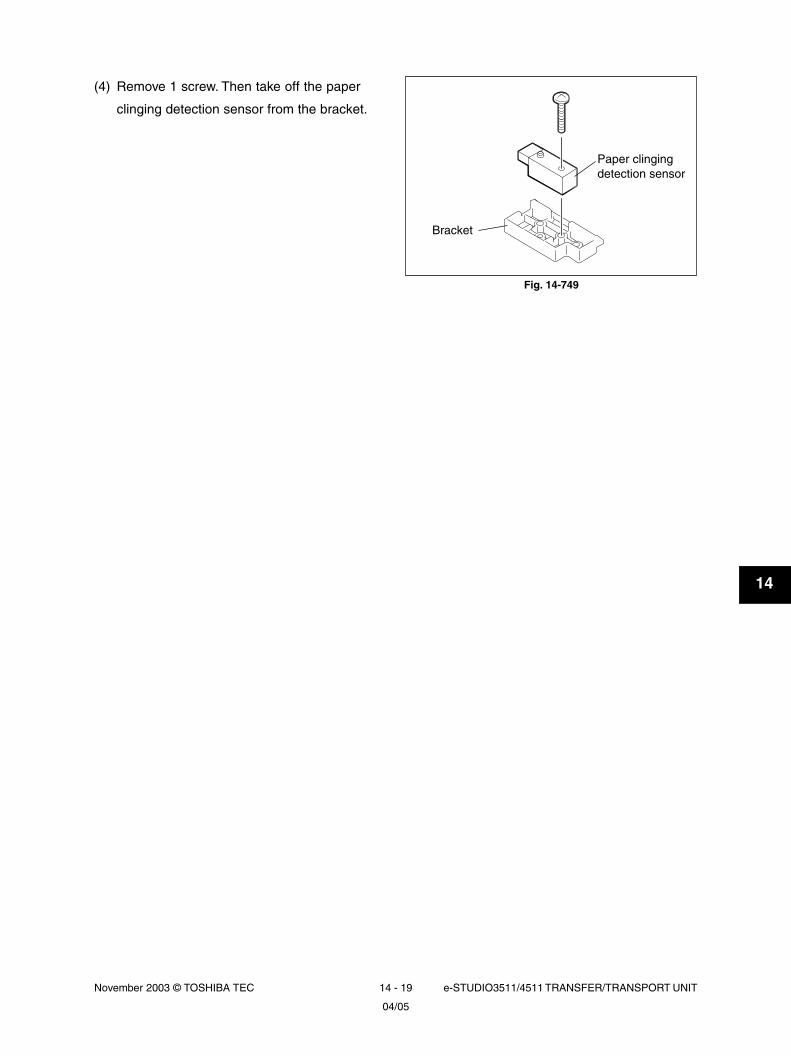
November 2003 © TOSHIBA TEC 14 - 19 e-STUDIO3511/4511 TRANSFER/TRANSPORT UNIT
14
Fig. 14-749
(4) Remove 1 screw. Then take off the paper
clinging detection sensor from the bracket.
Paper clingingdetection sensor
Bracket
04/05

e-STUDIO3511/4511 TRANSFER/TRANSPORT UNIT 14 - 20 November 2003 © TOSHIBA TEC
14

November 2003 © TOSHIBA TEC 15 - 1 e-STUDIO3511/4511 IMAGE QUALITY CONTROL
15
15. IMAGE QUALITY CONTROL
15.1 General DescriptionIn this equipment, image quality is controlled by the image quality sensor. At this control, image forming
conditions are automatically adjusted so as to minimize the change in the image density or tone repro-
duction caused by the fluctuation of working environment or life of supply items.
At first, the image quality sensor operates to output reflected light amount voltage when no toner image
is formed on the transfer belt. The output voltage is then converted analog-to-digital to be output as the
reflected light amount signal. The light source amount voltage of the sensor is adjusted to correspond
with the value set in advance and the output value of reflected light amount signal at this adjustment is
stored. This output value is considered as the reading of the belt surface. Next, the sensor outputs the
reflected light amount signal when a test pattern is developed on the transfer belt. This output value is
considered as the reading of the toner image.
The difference between the reading of the transfer belt and that of the toner image is defined as toner
adhesion amount. Image forming conditions are determined in approximating this toner adhesion amount
to the value set in advance.
In addition, a shutter operated by the solenoid is equipped on the light receiving/emitting surfaces to
prevent stain to the sensor and to calibrate the sensor with the reflection from the shutter.
15.2 Principle of the SensorImage quality sensor projects light onto the transfer belt and the toner image (test pattern) developed on
the transfer belt to output a voltage corresponding to the reflected light amount.
The output voltage is then converted analog-to-digital into reflected light amount signal. The CPU calculates
the toner adhesion amount to control the image forming conditions.
Fig. 15-201
CPUA/D
D/A
Transfer belt
Test pattern(toner image)
Light emittingelement
Light receivingelement
Reflected lightamount voltage
Reflected lightamount signal
Light sourceamount signal
Light source amount voltage

e-STUDIO3511/4511 IMAGE QUALITY CONTROL 15 - 2 November 2003 © TOSHIBA TEC
15
15.3 Flow Chart of Control Procedure
Start of control procedure (when meeting the image quality control starting conditions such as power-ON)
[1] The surface potential of photoconductive drum is estimated with the drum thermistor and tempera-
ture/humidity sensor.
[2] Reference image forming conditions are set.
[3] The sensor light source is adjusted.
[4] The test pattern is formed on the transfer belt.
[5] Toner adhesion amount of test pattern (high density) is calculated.
[6] Judgment
(whether the toner adhesion amount of the test pattern is within the acceptable
range or not)
NO
Modifies the image forming conditions.
YES
[7] Toner adhesion amount of the test pattern (low density) is calculated.
[8] Judgment
(whether the toner adhesion amount of the test pattern is within the acceptable
range or not)
NO Return to [8].
Modifies the image forming conditions.
YES
The test pattern is formed on the transfer belt.
[9] The image forming conditions are determined and stored in NVRAM.
[10] Control procedure is completed.
(The determined image forming conditions will be reflected on subsequent copies.)
Return to [4].
→→
→→
→→
→

November 2003 © TOSHIBA TEC 15 - 3 e-STUDIO3511/4511 IMAGE QUALITY CONTROL
15
15.4 Construction· Image quality sensor: Projects the amount of light on the transfer belt and outputs the voltage
corresponding to the reflected light amount from the transfer belt or the
toner image on the transfer belt.
· D/A converter: Converts light source amount signal into the voltage to the sensor.
· Laser optical system: Performs test pattern exposure (for toner image formation).
· A/D converter: Converts the output voltage from the sensor into digital values and outputs
them to the CPU.
· Image forming process: Performs charging, laser exposing and developing processes.
· CPU: Performs steps [1] to [10] described previously.
A/DD/A
CPU
Image forming process
Transfer belt
Reflected lightamount signal
Light sourceamount signal
Various image formingconditions
Image qualitysensor
Laser optical system
Fig. 15-401

e-STUDIO3511/4511 IMAGE QUALITY CONTROL 15 - 4 November 2003 © TOSHIBA TEC
15
15.5 Disassembly and Replacement[A] Image quality sensor / Image quality sensor
shutter solenoid
(1) Take off the fuser unit ( Chapter 16.7 [A]).
Take off the transfer belt unit ( Chapter 14.7
[A]).
(2) Open the 2nd transfer cover. Remove 2 screws
and disconnect 2 connectors. Take off the
image quality sensor assembly.
Note: Insert latches of sensor case to the hole of
the plate securely when installing.
(3) Remove 2 screws and take off the image quality
sensor.
(4) Remove 2 screws and take off the image quality
sensor shutter solenoid.
Fig. 15-501
Fig. 15-502
Image quality sensorshutter solenoid
Image quality sensor
Image quality sensor assemblyConnector

November 2003 © TOSHIBA TEC 16 - 1 e-STUDIO3511/4511 FUSER UNIT/PAPER EXIT SECTION
16
16. FUSER UNIT / PAPER EXIT SECTION
16.1 General DescriptionToner is fused by applying heat and pressure on the transferred image on the paper which is transported
to the fuser unit. The paper is then transported to the receiving tray, paper exiting options or ADU. The
fuser unit consists of the IH coil, fuser roller, pressure roller, fuser belt, separation roller, separation
fingers, separation plate, cleaning roller, oil roller, thermistors, thermostat, exit roller, exit sensor, etc.
Fig. 16-101
16.2 OperationThe fuser belt is located between the fuser roller and pressure roller. The fuser roller is pressed with the
spring force from the pressure roller side, and it is rotated by the transport motor drive. The fuser belt
also rotates simultaneously. Then the paper transported to the fuser unit is hold between the fuser belt
and pressure roller and the toner is fused on the paper with heat and pressure. After this, the separation
fingers, belt separation mechanism and separation plate separate the paper from the fuser belt. Then
the paper is transported to the receiving tray, paper exiting options or ADU through the exit roller. In
addition, the IH coil in the fuser roller does not structurally rotate.
The thermistors control the temperature of fuser roller and detect temperature abnormalities. If the
temperature becomes excessively high, the thermostat is opened to stop the power supply to the IH coil.
When transporting OHP film or thick paper in color modes, the transport speed is lowered to the range
from 1/2 to 1/4 in order to improve fusing efficiency. The exit motor which drives the exit roller is decelerated
at the same time.
Separation roller
Fuser belt
Separation finger
Pressure roller
IH coilThermistor
Thermostat
Fuser rollerOil roller
Cleaning roller
Separation plate
Exit sensor
Exit roller

e-STUDIO3511/4511 FUSER UNIT/PAPER EXIT SECTION 16 - 2 November 2003 © TOSHIBA TEC
16
16.3 Functions(1) IH coil (IH: Induction Heating)
The IH coil is inside the fuser roller and applies the induction heating to the fuser roller. This IH coil is
divided into two parts; the main IH coil heating the center of the fuser roller and the sub IH coil
heating both ends of the fuser roller. Each part turns ON/OFF individually controlling the balance of
electric supply so that the fuser roller can be kept at a certain temperature without wasting electric
power on any paper size.
(2) Fuser roller
The fuser roller is a metal roller which generates heat spontaneously with eddy current produced by
the electromagnetic induction of IH coil. The fuser belt is heated by this self-heating of this roller, and
then the toner is fused on the paper.
(3) Pressure roller
The pressure roller is a sponge roller which assures the nip amount between the fuser roller and
fuser belt. The pressure arm and spring press the fuser roller and fuser belt.
The toner is fused effectively by the pressure of this roller.
(4) Fuser belt
The fuser belt is hanged up between the fuser roller and separation roller and fuses the toner image
on the paper transported by being heated.
The thin fuser belt enables to reduce warming up time and mode changing time. To prevent the fuser
belt from adhering toner, the surface of the fuser belt is fluorinated.
(5) Separation roller
The separation roller is an extra small ceramic roller coated with the fluororesin tube. When the fuser
belt is tensed and driven by the separation roller, the fuser roller drives the fuser belt and the paper
between the fuser belt and pressure roller is separated from the fuser belt (belt separation method).
(6) Separation fingers
Five separation fingers are installed above the pressure roller to separate the paper stuck on the
pressure roller.
(7) Separation plate
The separation plate is installed above the separation roller to cover the insufficient separation often
occurs at color printing - the mode that the toner is much adhered.

November 2003 © TOSHIBA TEC 16 - 3 e-STUDIO3511/4511 FUSER UNIT/PAPER EXIT SECTION
16
(8) Cleaning roller / Oil roller
Silicone oil is contained inside of the oil roller to supply a proper amount of oil to the fuser belt, and
this enables to remove the residual toner and paper dust (preventing offsetting phenomenon). Also,
the cleaning roller is a fluorinated aluminum roller which removes the residual toner and paper dust
adhered on the oil roller.
(9) Main thermistor/Sub thermistor
This thermistor detects the temperature of the fuser belt to maintain it in a certain temperature
range (actually around 180°C) between the lower limit causing the poor fusing and the upper limit
causing the high temperature offsetting. When the temperature of the fuser belt is lower than the
preset temperature, it turns ON the power supply to the IH coil, and when it is higher than the preset
temperature, it cuts off the supply. The main thermistor detects the temperature of the center part of
the fuser belt and the sub thermistor detects the temperature of the both ends of the fuser belt. It
also detects the slight difference of the temperatures at the center and both ends of the fuser belt to
control the balance of ON/OFF of the center/side parts of IH coil to keep the fuser belt at a certain
temperature.
(10) Front edge thermistor
It detects the temperature abnormality at the both ends of the fuser belt. This area may be over-
heated without heat absorption by paper since paper does not pass through this area. This ther-
mistor is not related to the temperature control of the fuser belt.
(11) Thermostat
The thermostat cuts off the power supply to the IH coil by opening itself if the fuser belt becomes
abnormally hot as a result of the problem such as thermistor malfunction. The thermostat for this
equipment is used to prevent abnormal operation. When the thermostat detects any abnormality, it
must be replaced as well as the other damaged parts in the fuser unit.
(12) Exit sensor
This sensor detects the arrival of the leading or trailing edge of the paper at the exit roller of the
fuser unit. It also detects paper jams in the fuser unit paper exit section and trailing edge of paper
turned over for duplex printing.
(13) Exit motor
The exit motor is a stepping motor which drives the exit roller and bridge unit (option). It reduces the
transport speed down to the range from 1/2 to 1/4 according to the type of paper such as OHP film
or thick paper in color modes.
(14) Exit roller
This roller transports the paper from the fusing section to the receiving tray, paper exiting options or
the ADU and is driven by the exit motor.
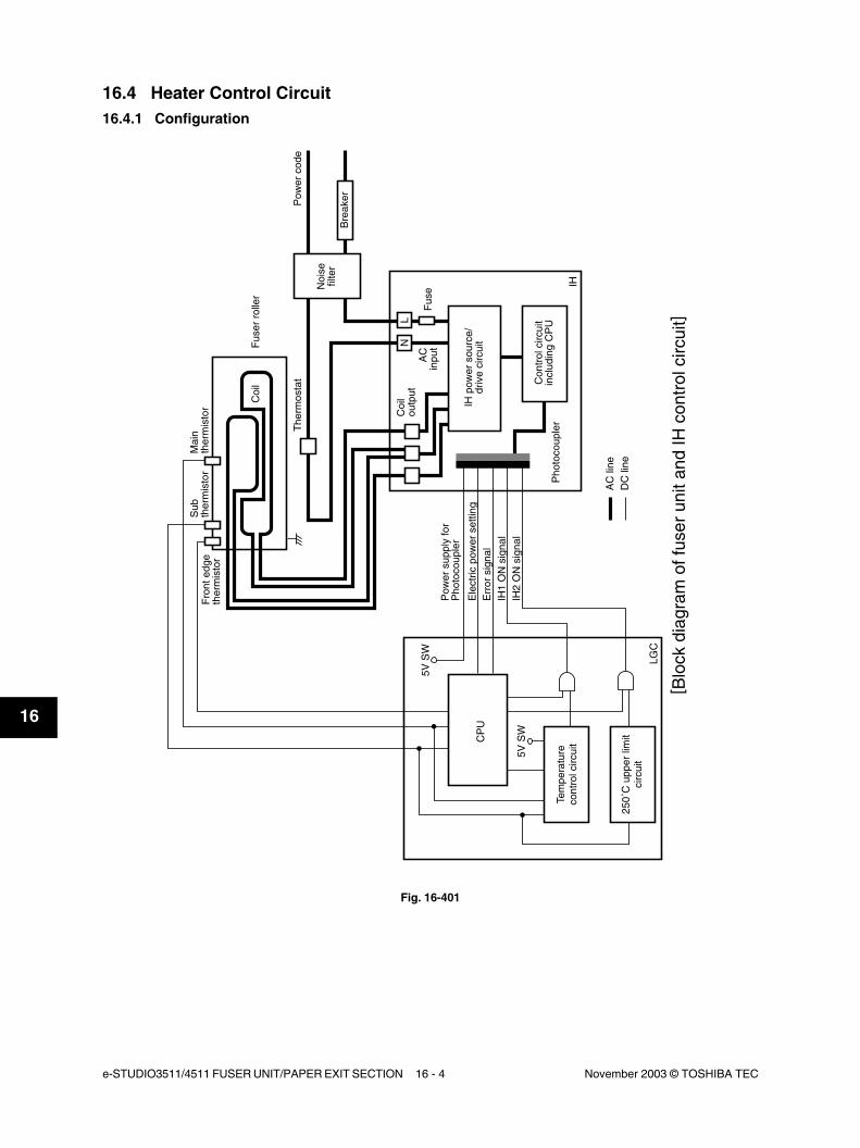
e-STUDIO3511/4511 FUSER UNIT/PAPER EXIT SECTION 16 - 4 November 2003 © TOSHIBA TEC
16
16.4 Heater Control Circuit16.4.1 Configuration
NL
CP
U
Tem
pera
ture
cont
rol c
ircui
t
250˚
C u
pper
lim
itci
rcui
t
LGC
IH
5V S
W
5V S
W
Mai
nth
erm
isto
rS
ubth
erm
isto
r
Coi
lF
user
rol
ler
Coi
lou
tput
Fus
eA
Cin
put
The
rmos
tat
Noi
sefil
ter
Bre
akerPow
er c
ode
Fro
nt e
dge
ther
mis
tor
IH p
ower
sou
rce/
driv
e ci
rcui
t
Con
trol
circ
uit
incl
udin
g C
PU
Pho
toco
uple
r
AC
line
DC
line
Pow
er s
uppl
y fo
rP
hoto
coup
ler
Ele
ctric
pow
er s
ettin
gE
rror
sig
nal
IH1
ON
sig
nal
IH2
ON
sig
nal
[ Blo
ck d
iagr
am o
f fus
er u
nit a
nd IH
con
trol
circ
uit]
Fig. 16-401

November 2003 © TOSHIBA TEC 16 - 5 e-STUDIO3511/4511 FUSER UNIT/PAPER EXIT SECTION
16
16.4.2 Heating principle of IH Heater
The magnetic field is generated by applying a high frequency current to the IH coil inside the fuser roller,
which then generates the eddy current in it. When the eddy current flows, the Joule heat is generated by
the resistance element of the fuser roller, which is then heated. In the IH coil method, the thermal efficiency
is higher than the lamp method because the fuser roller is directly heated.
IH coil is divided into two parts to decrease the temperature difference between the center and both ends
of the fuser roller.
B
A
Main IH coil Current flowing on the surface of the fuser roller
Current flowing inside thefuser roller
Eddy currentMagnetic fieldSub IH coil
High frequencypower source
D1
T1
C1C3
CPU
Voltageinput
I/F circuit on LGC board
Monitoring input current
Current input
Monitoring input current
Control circuit high frequency current
Smoothing circuit
Tr2
(IGBT)
C2
Tr1
IH coil
Fuser roller
IGBTdrive
IGBTdrive
Pho
toco
uple
r
[Image of Current Flowing form A to B]
Fig. 16-402
[Book Diagram of High Frequency Power Supply]
Fig. 16-403

e-STUDIO3511/4511 FUSER UNIT/PAPER EXIT SECTION 16 - 6 November 2003 © TOSHIBA TEC
16
CN No.
CN455-2
CN455-3
CN455-4
CN455-5
CN455-6
CN455-7
CN455-8
CN455-1
CN456-1
CN456-4
CN456-5
CN456-2
CN456-3
Name of single
+5VSW
H1PWR1
H1PWR2
H1PWR3
H2PWR1
H2PWR2
H2PWR3
IH2 ON
IH1 ON
H1ERR1
H1ERR2
SG
IHDUTY
Direction
LGC to IH
LGC to IH
IH to LGC
LGC to IT
Definition
Switching signal of power setting
IH coil energization permitting signal
IH status signal (*Note)
Main/sub switching signal
16.4.3 IH control circuit interface
The IH control circuit uses a photocoupler as an insulation against the secondary circuit.
The interface signals are as follows.
(*Note) IH status signal
• When the temperature (due to insufficient cooling) of the switching element (IGBT) is
abnormal:
“12: Coil is abnormal, IH FAN OFF” → After a certain period of time → Error [C480]
• Main/sub coil continuous energization error (15 sec.): “12: Coil is abnormal, IH FAN OFF” →
After a certain period of time → Error [C480]
• When the upper limit of the power voltage is abnormal:
“10, 11, 14: Initializing” → After a certain period of time → Error [C470]
“07: Ready” → After a certain period of time → Error [C470]
• When the lower limit of the power voltage is abnormal:
“10, 11, 14: Initializing” → After a certain period of time → Error [C470]
“07: Ready” → After a certain period of time → Error [C470]
• Defective circuits →: “13: Abnormal circuit, IH coil abnormality” → Error [C490]
• Ready state after the initialization: “01: Ready”

November 2003 © TOSHIBA TEC 16 - 7 e-STUDIO3511/4511 FUSER UNIT/PAPER EXIT SECTION
16
16.4.4 Relation between system configuration and IH output
for NAD, SAD, TWD:
* RADF: Reversing automatic document feeder, FIN: Finisher, HPU: Hole punch unit, LCF: Large
capacity feeder, FAX: FAX unit
(*1) The wattage lowers 50 W more when the scanning is performed from the RADF during warming up.
(*2) AC power should be input voltage when the equipment is warming up (The lower the voltage is, the
longer the warming up time becomes).
System configuration
Equipment only
Equipment and
RADF (*1)
Equipment, RADF (*1)
and FIN
Equipment, RADF (*1),
FIN, and HPU
Equipment, RADF (*1),
FIN, HPU and LCF
Equipment, RADF (*1),
FIN, HPU, LCF and
FAX
Warming up (*2)
1160-1300W
1160-1260W
1140-1240W
Ready
800W
Printing
1080W
1020W
960W
940W
Energy savingmode
800W
AutomaticallyOFF
OFF
Warming uptime
Approx
40 sec.
for ASD, AUD, CND:
System configuration
Equipment only
Equipment and
RADF (*1)
Equipment, RADF (*1)
and FIN
Equipment, RADF (*1),
FIN, and HPU
Equipment, RADF (*1),
FIN, HPU and LCF
Equipment, RADF (*1),
FIN, HPU, LCF and
FAX
Warming up (*2)
1160-1300W
1160-1260W
1140-1240W
Ready
700W
Printing
1240W
1180W
1120W
1100W
Energy savingmode
700W
AutomaticallyOFF
OFF
Warming uptime
Approx
40 sec.
04/10

e-STUDIO3511/4511 FUSER UNIT/PAPER EXIT SECTION 16 - 8 November 2003 © TOSHIBA TEC
16
16.4.5 Temperature detection section
To maintain the stable temperature of the fuser belt, the thermistor detects the temperature and controls
ON/OFF of the IH coil. Output from the thermistors is used to detect the abnormality.
(1) Relation between the thermistor output voltage and surface temperature of the fuser belt:
°C
180
0
Ready (180°C)Warming-up
Temperatureof fuser belt
During printing (180°C)
OFFIH coil ON ON OFF ON OFF ON OFF OFFON ON
Fig. 16-404
(3) Temperature control for the both ends of the fuser belt
During the continuous printing, the temperature of the both ends of the fuser belt (areas where the
paper does not pass on) generally tend to be higher than that of the other areas (areas where the
paper passes on). The temperature of the ends are detected by the front edge thermistor, and when
it reaches 250°C, the heater is automatically turned OFF regardless of the temperature of the area
where the paper passes on.
(2) Control of the surface temperature of the fuser belt:
Output voltages of thermistors [V]
Approx. 0.30
Approx. 1.77
Approx. 3.28
Approx. 3.66
Approx. 3.81
Approx. 4.03
Surface temperatures of fuser belt [oC]
40
100
150
170
180
200

November 2003 © TOSHIBA TEC 16 - 9 e-STUDIO3511/4511 FUSER UNIT/PAPER EXIT SECTION
16
(4) Temperature control at energy saving mode
This equipment has the following two types of temperature control for saving energy and returns to
ready status to perform printing in each mode upon printing request.
The period of time from the printing request to this mode can be set in the Setting Mode (08) or by an
from administrator.
Administrator setting procedure:
[USER FUNCTIONS] button → [ADMIN] (input of administrator’s password) → [GENERAL] →
[ENERGY SAVER]
Auto Power Save Mode (Setting Mode (08-205)):
When the printing is not performed in a specified period of time (default setting: 15 min.) after the
previous printing is completed, the equipment enters to Auto Power Save Mode. ON/OFF of IH coil
is controlled to maintain the fuser belt surface temperature at 100oC.
Auto Shut Off Mode (Setting Mode (08-206)):
When the printing is not performed in a specified period of time (default setting: e-STUDIO3511: 60
min. / e-STUDIO4511: 90 min.) after the equipment entered to Auto Power Save Mode, the equip-
ment then enters to Auto Shut Off Mode to turn OFF the IH coil.
OFF
Warming-up Ready During printing Fixed time (08-205)
Fixed time (08-206)
Auto Power SaveMode Auto
Shut OffMode
100
C
180
0
Temperatureof fuser belt
IH coil ON
Fig. 16-405
e-STUDIO3511/4511 FUSER UNIT/PAPER EXIT SECTION 16 - 10 November 2003 © TOSHIBA TEC
16
Reference
* The thermistor/heater status counter never has values other than 0 to 19.
• If the IH coil does not turn ON and the service call [C410] is displayed immediately after the
power is ON, ensure the thermistor/heater status counter is “2” or over. If it is “2” or over, be
sure to check the thermistor, thermostat and IH coil. Reset the counter to “0” (setting mode
(08-400)) after repairing them, then turn ON the power.
• If the thermistor/heater status counter is “20” or over (e.g., 21), the data in NV RAM or NV
RAM itself may possibly have been ruined due to causes such as leakage from the chargers.
Check the bias, high-voltage transformers and charge wires to see if any of them is defective,
and also look through all the data in the NV RAM.
(5) Thermistor/heater status counter control
• To enhance the safety of the fusing section unit, CPU provides the following protection: When the
third [C410] error has occurred after two consecutive [C410] errors, the IH coil is not turned ON
and error [C410] is displayed immediately even if an operator turns OFF the power and back ON.
However, if the equipment goes into a ready state normally with the thermistor/heater status counter
“1” or below, the counter is cleared to “0”.
• If the error codes [C410] to [C450] are displayed and still not cleared even thought the thermistor,
thermostat and IH coil have been repaired (and the power ON/OFF does not clear the error), check
the Setting Mode (08-400) to set the thermistor/heater status counter to “0”.
November 2003 © TOSHIBA TEC 16 - 11 e-STUDIO3511/4511 FUSER UNIT/PAPER EXIT SECTION
16
(6) Temperature detection configuration
Thermistor is a device whose resistance decreases as it detects a higher temperature. Thus its input
voltage to CPU changes and then CPU judges whether this change is normal or abnormal. If one of
the fuser belt thermistors is broken, the control circuit judges that the fuser belt temperature is ex-
tremely low and keeps turning the IH coil ON. As a result, the fuser belt temperature rises, and
possibly activates the thermostat which is a safety protection device. To prevent this in advance,
CPU works to detect whether each thermistor is broken or not.
Also, the thermistors constantly check the temperature of IH coil to prevent it from excessive heating
by IH circuit abnormality, LGC circuit abnormality or thermistor abnormality. The thermistors auto-
matically turn OFF the power when the temperature of IH coil exceeds the specified temperature.
139
138
137PC4/AN4
PC5/AN5
PC6/AN6
CPU
+5Front edgethermistor
Mainthermistor
Subthermistor
+5
+5
Fig. 16-406

e-STUDIO3511/4511 FUSER UNIT/PAPER EXIT SECTION 16 - 12 November 2003 © TOSHIBA TEC
16
Checking timing
Power ON
Detecting
40°C
Detecting
100°C
Detecting
160°C
Detecting
ready
temperature
During ready
status
At energy
saving mode
During printing
At paper jam
Condition
1
2
1
2
1
2
1
2
1
2
1
2
1
2
1
2
Main thermistor
250°C or above
-
40°C or below
150°C or above
250°C or above
-
40°C or below
-
250°C or above
-
100°C or below
-
40°C or below
150°C or above
250°C or above
-
160°C or below
-
40°C or below
150°C or above
250°C or above
-
Ready temp. or below
-
40°C or below
160°C or above
250°C or above
-
40°C or below
-
40°C or below
160°C or above
250°C or above
-
-
40°C or below
-
-
250°C or above
-
Sub thermistor
-
250°C or above
150°C or above
40°C or below
-
250°C or above
-
40°C or below
-
250°C or above
-
100°C or below
150°C or above
40°C or below
-
250°C or above
-
160°C or below
150°C or above
40°C or below
-
250°C or above
-
Ready temp. or below
160°C or above
40°C or below
-
250°C or above
-
40°C or below
160°C or above
40°C or below
-
250°C or above
-
-
40°C or below
-
-
250°C or above
Front edge thermistor
-
-
-
-
-
-
-
-
-
-
-
-
-
-
-
-
-
-
-
-
-
-
-
-
-
-
-
-
-
-
-
-
-
-
250°C or above
-
-
40°C or below
-
-
Error
code
C440
C410
C440
C410
C440
C430
C440
C430
C440
C430
C440
C430
C440
C450
C440
Checking
timing
Power ON
Fixed time
Fixed time
Fixed time
Fixed time
On usual
On usual
On usual
(7) Abnormality detection by the thermistors
The following table shows the conditions judging the fuser belt temperature abnormality and detecting timing.
Temperature judged
* Condtion: Priority of error checking.

November 2003 © TOSHIBA TEC 16 - 13 e-STUDIO3511/4511 FUSER UNIT/PAPER EXIT SECTION
16
16.4.6 Abnormality in the IH control circuit
When an abnormality is detected in the IH control circuit, it stops the power supply to the IH coil and
displays a message “Call for service”.
(1) IH control circuit
CPU output level of the IH control circuit changes depending on the condition of IH coil. This output
level goes through the photocoupler into the gate array.
PA4
VDDIH
PA3
5V SW
H1ERR2
H1ERR1
LGC
CPU
Gate array
Fig. 16-407

e-STUDIO3511/4511 FUSER UNIT/PAPER EXIT SECTION 16 - 14 November 2003 © TOSHIBA TEC
16
Error content
Initial abnormality
IH power voltage abnormality
IGBT high temperature abnormality /
Continuous energization (15 sec.)
IH circuit/coil abnormality
IH power voltage abnormality
IGBT high temperature abnormality /
Continuous energization (15 sec.)
IH circuit/coil abnormality
IH power voltage abnormality
IGBT high temperature abnormality /
Continuous energization (15 sec.)
IH circuit/coil abnormality
Normal
Checking timing
Power ON
In warming up
Detecting 40°C
In warming up
Detecting 40°C
During ready status
During ready status
During printing
At Energy Saving Mode
H1ERR1
L
L
L
H
L
L
H
L
L
H
H
Error code
C470
C470
C480
C490
C470
C480
C490
C470
C480
C490
-
H1ERR2
L
L
H
H
L
H
H
L
H
H
L
(2) IH error
Port input value
Initial abnormality:CPU (IH) abnormality is not cleared.
IH power voltage abnormality:The input voltage becomes above 20% (approx.) or below 20% (approx.) of the rated voltage.
IGBT high temperature abnormality:Overheating of IGBT or short- or open-circuit of IGBT temperature-detecting sensor.
IH circuit abnormality:Abnormality in IH circuit
IH coil abnormality:Temperature-detecting sensor in IH circuit is abnormal, or IH coil is open-circuited or wrongly in-stalled.

November 2003 © TOSHIBA TEC 16 - 15 e-STUDIO3511/4511 FUSER UNIT/PAPER EXIT SECTION
16
16.5 Control Circuit of Exit MotorThe following is the control circuit of the exit motor.
The exit motor is a stepping motor. The motor is turned ON/OFF and the direction of its rotation is
switched by controlling the output timing of pulse signal (A0·A1·B0·B1).
G14 G22
G24
G20
G48
G16 Exit roller(φ15)
Exit motor
PG10
PG12
PG11
PG13
CPU
EXTMA
EXTMB
EXTMC
Exit Motor
EXTMD
EXTMA-0
+5V
EXTMB-0
EXTMC-0
EXTMD-0
STK672
A
AB
B
BB
A1
B1
A0
B0
VREFPG0
PG1LCA301
PG2
5V SW
LGC DRV
Fig. 16-501
16.6 Exit Motor DriveThe diagram shown below is the layout of the driving gears of the exit roller.
Fig. 16-601

16
e-STUDIO3511/4511 FUSER UNIT/PAPER EXIT SECTION 16 - 16 November 2003 © TOSHIBA TEC
Fig. 16-701
Fig. 16-702
Fig. 16-703
Fig. 16-704
Transport guide
Jam access cover
Cleaning unit
16.7 Disassembly and Replacement[A] Fuser unit
(1) Take off the IH terminal cover ( Chapter 2.5.1[K])
(2) Disconnect 2 connectors and 4 fastonterminals.
Notes:1. Make sure to hold the plastic part of thefaston terminals when disconnectingthem.
2. Make sure not to connect each terminalto the wrong position.
(3) Remove 2 screws and take off the fuser unit.
[B] Oil roller
(1) Take off the fuser unit ( Chapter 16.7 [A]).
(2) Open the jam access cover and transport guide.
(3) Remove 2 screws and take off the cleaning unit
by lifting it up.
Note: When installing, fit 2 protrusions on the
bottom of the cleaning unit into the holes of
the frame securely.
RED(S)
BLUE(C)
WHITE
WHITE

16
November 2003 © TOSHIBA TEC 16 - 17 e-STUDIO3511/4511 FUSER UNIT/PAPER EXIT SECTION
Fig. 16-705
Fig. 16-706
Fig. 16-708
(6) Remove 1 bushing from each side of the oil
roller.
Spring (B)
(4) Remove spring (B) on each end of the oil roller.
(5) Take off the oil roller.
- Front side -
- Rear side -
Note: Install the oil roller according to the marking
on the frame (the shaft end with a groove
should point at the rear side).
Fig. 16-707
[C] Cleaning roller
(1) Take off the oil roller from the cleaning unit ( Chapter 16.7 [B]).
(2) Remove 1 E-ring and 1 bushing from thecleaning roller front side. Then take off thecleaning roller.
(3) Remove the spring (A) on each end of theframe.
Note: When installing, make sure that the oil rollerrotates smoothly by turning the gear (C) ofthe cleaning roller manually for a severaltimes.
Oil roller
Cleaning roller
Spring (A)
Groove
Gear (C)
Bushing
E-ring
Bushing

16
e-STUDIO3511/4511 FUSER UNIT/PAPER EXIT SECTION 16 - 18 November 2003 © TOSHIBA TEC
Fig. 16-711
Fig. 16-712
C
S
Bracket
Spring
Spring
E-ring
Fig. 16-710
[D] IH coil
(1) Take off the fuser unit ( Chapter 16.7 [A]).
(2) Release the harnesses from 5 harness clamps.
Then remove 1 E-ring, 1 bushing and 2 screws.
(3) Pull out the bracket and IH coil.
(4) Take out the IH coil from the bracket.
Notes:1. When installing, be sure to set the
harnesses “C” and “S” of 4 harnesses on
upper.
2. Make sure that there is not any scratch
or break on the white tube on the IH coil.
3. Make sure that there is not any peeling
or scratch on the harness tube.
White tube
[E] Fuser roller / Fuser belt guide
Note: When installing/disinstalling the fuser roller,
make sure not to remove the spring (shown
in the figure at right) since the removal of
this spring may have the fuser roller press
to deform the thermistor.
- Front side -
- Rear side -
(4) Remove 1 E-ring, the gear (C) and 1 bushing
from the cleaning roller rear side.
Fig. 16-709
Gear (C)
Bushing
E-ring
Bushing
IH coil

16
November 2003 © TOSHIBA TEC 16 - 19 e-STUDIO3511/4511 FUSER UNIT/PAPER EXIT SECTION
Fig. 16-715
Fig. 16-716
Bracket
Fig. 16-714
Bearing
(5) Remove 1 bearing.
(6) Insert a flat-head screwdriver into the slit of the
fuser belt guide on the rear side. Then slide
the plate while opening the slit by the flat-head
screwdriver. Take off the fuser belt guide from
the fuser roller.
Note: Be careful not to scratch the fuser belt.
Fuser belt guide Fuser belt
(7) Remove 2 screws and take off the bracket.
(1) Remove the cleaning unit ( Chapter 16.7 [B]).
(2) Remove the IH coil ( Chapter 16.7 [D]).
(3) Push down the pressure releasing levers on
both sides.
(4) Remove 1 C-ring and 2 gears.
Fig. 16-713
C-ringGearPressure releasing
lever

16
e-STUDIO3511/4511 FUSER UNIT/PAPER EXIT SECTION 16 - 20 November 2003 © TOSHIBA TEC
Fig. 16-720
Fig. 16-719
(4) Remove 1 screw and take off the bracket on
the rear side.
Fuser belt unit
Fig. 16-718
[F] Fuser belt
(1) Take off the fuser roller ( Chapter 16.7 [E]).
(2) Lift up the fuser belt unit and take it off.
Note: Be careful not to scratch the fuser belt. Lay
the fuser belt on the clean place to prevent
the belt from the dust.
(3) Remove 1 screw and take off the bracket on
the front side.
Bracket
Bracket
(8) Take off the fuser roller.
(9) Remove 1 C-ring, 1 bearing and 1 fuser belt
guide from the fuser roller front side.
Note: When installing, make sure that the fuser belt
guide securely fits in the fuser roller groove.
Also, make sure that the ring on the fuser
belt guide securely fits in the groove on the
belt restricting plate.
Fig. 16-717
Fuser roller
Fuser belt guide C-ring
Ring
Bearing
Fuser belt
- Front -
- Rear -

16
November 2003 © TOSHIBA TEC 16 - 21 e-STUDIO3511/4511 FUSER UNIT/PAPER EXIT SECTION
Fig. 16-724
Note: When installing the fuser belt, place a sheet
of paper between the separation plate and
fuser belt in order to prevent the fuser belt
from being scratched by the separation plate.
Keep the paper between then until the fuser
roller is installed.
Fig. 16-723
Paper
Fuser belt unit
Fuser belt
Fig. 16-722
(6) Lift up the separation roller by sliding it.
(7) Take off the fuser belt.
Separation roller
Fuser belt
Separationplate
[G] Separation finger
(1) Take off the fuser roller ( Chapter 16.7 [E]).
(2) Lift up the fuser belt unit and take it off.
Note: Be careful not to scratch the fuser belt. Lay
the fuser belt on the clean place to prevent
the belt from the dust.
Fig. 16-721
(5) Remove 1 E-ring. Then remove 1 bearing.
E-ring
Bearing
Separation plate
Fuser belt

16
e-STUDIO3511/4511 FUSER UNIT/PAPER EXIT SECTION 16 - 22 November 2003 © TOSHIBA TEC
Fig. 16-728
Fig. 16-727
Separation finger unit
Separation finger
Fig. 16-726
Spring
(4) Remove 2 springs.
(5) Remove 2 screws and take off the separation
finger unit.
(6) Remove the spring of each separation finger.
Spring
Fig. 16-725
(3) Confirm that the pressure releasing levers on
both sides are up. Then loosen each 1 screw
on both front and rear sides.
- Front side -
- Rear side -

16
November 2003 © TOSHIBA TEC 16 - 23 e-STUDIO3511/4511 FUSER UNIT/PAPER EXIT SECTION
Fig. 16-732
Fig. 16-731
Cleaning unit
Thermostat unit
Pressure roller
Fig. 16-730
Bushing
BearingRing
(4) Remove each 1 ring, 1 bearing and 1 bushing
on both front and rear sides of the pressure
roller.
[I] Thermostat
(1) Take off the fuser unit ( Chapter 16.7 [A]).
(2) Remove 2 screws. Lift up the cleaning unit and
take it off.
Note: When installing, fit 2 protrusions on the
bottom of the cleaning unit into the holes of
the frame securely.
(3) Release the harnesses from the harness
clamps.
(4) Remove 2 screws and take off the thermostat
unit.
Note: Be careful not to scratch the fuser belt.
Fuser belt
Fig. 16-729
Pressure roller
[H] Pressure roller
(1) Take off the fuser belt unit ( Chapter 16.7 [F]).
(2) Take off the separation finger unit ( Chapter
16.7 [G]).
(3) Take off the pressure roller.
16
e-STUDIO3511/4511 FUSER UNIT/PAPER EXIT SECTION 16 - 24 November 2003 © TOSHIBA TEC
Fig. 16-736
Notes: When installing, pay attention to the
followings:
1. Make sure to fix the thermostat, and then
harness terminal in order on the bracket.
2. Make sure to keep the gap between the
fuser roller and thermostat is 0.7 mm to
2.0 mm while the fuser roller is pressed
to the pressure roller.
Fig. 16-735
Fig. 16-734
[J] Thermistor
(1) Take off the fuser unit ( Chapter 16.7 [A]).
(2) Release the harnesses from the harness
clamps.
(3) Remove 1 screw of each thermistor and take
off total 3 thermistors.
Thermostat(5) Remove 2 screws and take off the thermostat
from the bracket.
Fig. 16-733
Bracket
0.7-2.0mm

16
November 2003 © TOSHIBA TEC 16 - 25 e-STUDIO3511/4511 FUSER UNIT/PAPER EXIT SECTION
Fig. 16-740
Fig. 16-738
Fig. 16-739
[K] Exit sensor / Exit finger / Transport guide
(1) Take off the fuser unit ( Chapter 16.7 [A]).
(2) Open the jam access cover and transport guide.
(3) Remove 3 screws and take off the cover (A).
(4) Remove 1 screw and plate spring.
(5) Disconnect 1 connector and take off the exit
sensor.
(6) Remove 1 spring.
(4) Remove each 1 screw and take off the
thermistor from each bracket.
Note: When installing, be careful not to deform the
thermistor or the frame (plate). Also, make
sure that the thermistor is in touch with the
fuser belt.
Fig. 16-737
Cover (A)
SpringConnector
(7) Remove 1 E-ring and pull out the shaft. Then
remove 8 exit fingers and 1 actuator.
Exit sensorPlate spring
Actuator
E-ring

16
e-STUDIO3511/4511 FUSER UNIT/PAPER EXIT SECTION 16 - 26 November 2003 © TOSHIBA TEC
Fig. 16-743
Bushing
E-ring
Fig. 16-742
Exit roller cover
(8) Remove 1 screw.
(9) Enlarge the frame and take off the transport
guide.
[L] Exit roller
(1) Take off the fuser unit ( Chapter 16.7 [A]).
(2) Open the jam access cover of the fuser unit.
(3) Remove 2 screws (one of the front side is a
shoulder screw) and take off the exit roller
cover.
(Shoulder screw)
(4) Remove 1 E-ring and 1 bushing from the exit
roller front side.
Fig. 16-741
3
2
1
Fig. 16-744
Gear unit Bushing
E-ringE-ring
(5) Remove E-ring, gear unit, E-ring and bushing
in order from the exit roller rear side. Then take
off the exit roller.
Exit roller
Exit roller

16
November 2003 © TOSHIBA TEC 16 - 27 e-STUDIO3511/4511 FUSER UNIT/PAPER EXIT SECTION
Fig. 16-747
Fig. 16-748
IH board
IH control boardcooling fan cover
Fig. 16-745
Fig. 16-746
IH board cover
ConnectorIH board case
Connector
[M] IH control PC board (IH board)
(1) Take off the SYS board case ( Chapter 2.5.2
[C]).
(2) Take off the flywheel ( Chapter 9.5 [A]).
(3) Take off the right rear cover ( Chapter 2.5.1
[L]).
(4) Disconnect 2 connectors and 4 faston terminal
( Chapter 16.7 [A]).
(5) Remove 3 screws and take off the IH board
cover.(6) Disconnect 2 connectors, remove 2 screws and
take off the IH board case.
(7) Disconnect 4 connectors, remove 7 screws and
take off the IH board.
Notes: 1. Make sure not to connect each IH
connection cable to the wrong position.
2. Tighten 4 screws of the IH connection
cable completely (tightening torque: 1.17
- 1.56 N·m).
3. Since the IH control board is a high-
voltage section, make sure to disconnect
the power cable at maintenance.
IH connection cable
[N] IH control board cooling fan
(1) Take off the IH board case ( Chapter 16.7
[M]).
(2) Remove 1 screw and take off the IH control
board cooling fan cover.

16
e-STUDIO3511/4511 FUSER UNIT/PAPER EXIT SECTION 16 - 28 November 2003 © TOSHIBA TEC
(3) Disconnect 1 connector and take off the IH
control board cooling fan.
FLO
W
IH control boardcooling fan
Fig. 16-749
Connector
Fig. 16-750
Fig. 16-751
Fig. 16-752
[O] Scraper
(1) Take off the fuser unit ( Chapter 16.7 [A]).
(2) Remove 2 screws and take off the jam access
cover.
(3) Remove 4 screws and take off the cover.
(4) Remove 2 screws and take off the scraper.
Notes:1. Before installing or taking off the scraper,
confirm that the pressure releasing levers
are up.
2. Be careful not to scratch the fuser belt.
Scraper
04/01

17
November 2003 © TOSHIBA TEC 17 - 1 e-STUDIO3511/4511 AUTOMATIC DUPLEXING UNIT
17. AUTOMATIC DUPLEXING UNIT (ADU)
17.1 General DescriptionThe Automatic Duplexing Unit (ADU) is a unit to automatically print on both sides of paper. A switchback
method using the exit roller is adopted for the ADU of this equipment.
A sheet of paper is switchbacked by the exit roller right after the printing operation (fusing operation) on
one side is completed, and the reversed sheet is transported to the registration section for the other side
of the sheet to be printed.
The ADU mainly consists of the transport rollers and their drive system, paper guide and ADU entrance/
exit sensor.
Upper transport roller
Paper guide
Middle transport roller
ADU motor
ADU exit sensor
Exit guide
Lower transport roller
Entrance guide
ADU entrance sensor
Fig. 17-101

e-STUDIO3511/4511 AUTOMATIC DUPLEXING UNIT 17 - 2 November 2003 © TOSHIBA TEC
17
17.2 Description of OperationsThe back side printing (recording data of the back side of paper) is performed first by selecting duplex
printing mode and pressing the [START] button. When the trailing edge of the paper passes the exit gate,
the paper is switchbacked by the exit roller and transported into the ADU (the exit gate is closed with its
own weight), and then the switchbacked paper is transported with acceleration. The transportation de-
celerates in front of the upper transport roller of the ADU. The front side printing (recording data of the
front side of paper) is performed at the registration section. The paper passes through the exit gate again
and is transported to the receiving tray to complete duplex printing.
There are three methods of judging a paper jam: (1) whether the ADU entrance sensor is turned ON or
not in a specified period of time after the switchback to the ADU started (E510). (2) whether the ADU exit
sensor is turned ON or not in a specified period of time after the ADU entrance sensor is turned ON
(E520). (3) whether the registration switch is turned ON or not in a specified period of time after the paper
feeding from the ADU to the equipment (E110).
If the ADU is opened during duplex printing, the ADU motor and ADU clutch are stopped, namely, ADU
open jam occurs (E430).
The equipment is never to be stopped during printing by interruption in any case except paper jam or
service call.
The operation of the duplex printing differs depending on the size of the paper; single-paper circulation
and alternateness circulation. The figures in the following pages show the circulating operations during
duplex copying. The numbers in the figures indicate the page numbers.

17
November 2003 © TOSHIBA TEC 17 - 3 e-STUDIO3511/4511 AUTOMATIC DUPLEXING UNIT
(a) Single-paper circulation
With the paper larger than A4/LT size, duplex printing (back-side printing → front-side printing) is
performed for one sheet at a time as shown below.
Fig. 17-201
( 1 ) ( 2 ) ( 3 )
( 4 ) ( 5 ) ( 6 )
( 7 ) ( 8 ) ( 9 )
2
2
2
4
4
4
4
1
2
21
1
2
1
2
1
2
1
4
3
2
1
3

e-STUDIO3511/4511 AUTOMATIC DUPLEXING UNIT 17 - 4 November 2003 © TOSHIBA TEC
17
(b) Double-paper alternateness circulation
With A4/LT size paper or smaller, duplex printing is performed for two sheets at a time as shown
below.
Back side of the 1st sheet → Back side of the 2nd sheet → Front side of the 1st sheet → Front side
of the 2nd sheet
Fig. 17-202
( 1 ) ( 2 ) ( 3 )
( 4 ) ( 5 ) ( 6 )
( 7 ) ( 8 )
2
2
2
2
4
44
4
2
2
1
2
1
4
3
3
1

17
November 2003 © TOSHIBA TEC 17 - 5 e-STUDIO3511/4511 AUTOMATIC DUPLEXING UNIT
(c) Multiple-paper circulation
With more than one sheet of A4/LT size paper or smaller, duplex printing is performed as shown below in
a following order:
(In case of 5 sheets)
Back side of the 1st sheet ( 2 ) → Back side of the 2nd sheet ( 4 ) → Front side of the 1st sheet ( 1 ) →
Back side of the 3rd sheet ( 6 ) → Front side of the 2nd sheet ( 3 ) → Back side of the 4th sheet ( 8 ) →
Front side of the 3rd sheet ( 5 ) → Back side of the 5th sheet ( 10 ) → Front side of the 4th sheet ( 7 ) →
Front side of the 5th sheet ( 9 )
Fig. 17-203
( 1 ) ( 2 ) ( 3 ) ( 4 )
( 5 ) ( 6 ) ( 7 ) ( 8 )
( 9 ) ( 10 ) ( 11 ) ( 12 )
( 13 ) ( 14 ) ( 15 )
2
2
4
2
2 4
4
4
6
68 810
10 10
10
10
2 4
6
2
2
1
8
6
5
9
8
7
3
1
4 4
3
88
7
6 6
5 53
1
9
1

e-STUDIO3511/4511 AUTOMATIC DUPLEXING UNIT 17 - 6 November 2003 © TOSHIBA TEC
17
Timing chart for duplex copying from upper drawer (A4, 3 sheets)
7430
9060
9670
1105
511
655 11
985
1323
514
870
5955
6990
8200
9230
1044
011
46511
760 12
795
1400
015
030
1624
017
270
058
1059
5080
5087
8510
28510
420
1161
511
905
1385
014
795
1607
0
4835
5895
7075
Exi
t sen
sor
Reg
istr
atio
nse
nsor
Reg
istr
atio
ncl
utch
AD
U e
ntra
nce
sens
or
AD
U c
lutc
h
AD
U e
xit s
enso
r
AD
U m
otor
AD
U
Equ
ipm
ent
8135
9315
1037
0 1063
511
695
1287
513
935
1511
516
175
7935
9060
1017
011
05511
655 11
985
1373
014
870
8340
9580
1057
513
150
1414
515
390
7770
8660
1000
510
900
1357
514
470
(uni
t: m
sec)

17
November 2003 © TOSHIBA TEC 17 - 7 e-STUDIO3511/4511 AUTOMATIC DUPLEXING UNIT
Timing chart for duplex copying from upper drawer (A3, 1 sheet)
8510
1012
510
690
1213
5
6040
8070
1151
013
840
069
0010
050
1266
0
4915
6990
1069
012
765
8990
1018
510
690
1213
5
9405
1195
5
8830
1124
0
Exi
t sen
sor
Reg
istr
atio
nse
nsor
Reg
istr
atio
ncl
utch
AD
U e
ntra
nce
sens
or
AD
U c
lutc
h
AD
U e
xit s
enso
r
AD
U m
otor
AD
U
Equ
ipm
ent
(uni
t: m
sec)

e-STUDIO3511/4511 AUTOMATIC DUPLEXING UNIT 17 - 8 November 2003 © TOSHIBA TEC
17
17.3 Drive of ADUWhen the ADU motor rotates to the direction A, the upper transport roller is rotated driven by the gears
and belt. The ADU clutch is then turned ON and the middle transport roller and lower transport roller are
rotated.
Upper transport roller
Middle transport roller
ADU motor
ADU clutch
Lower transport roller
A
Fig. 17-301

17
November 2003 © TOSHIBA TEC 17 - 9 e-STUDIO3511/4511 AUTOMATIC DUPLEXING UNIT
17.4 Flow Chart
Fig. 17-401
Yes
Yes
A
ADU transport jam (E520)
ADU clutch ON
No
No
Yes
No
ADU transport jam (E510)
ADU entrancesensor ON?
ADU motor ON
Specified time has passed
Specified time has passed
Exit motor reverserotation ON
Specified time has passed(Paper is transported to the first
stopping position in ADU)
Trailing edge offirst paper turnedON the ADU exit
sensor?
ADU exit sensorcheck the arrival
ADU motor stoppedADU motor ON

e-STUDIO3511/4511 AUTOMATIC DUPLEXING UNIT 17 - 10 November 2003 © TOSHIBA TEC
17
Fig. 17-402
Yes
Yes
ADU misfeeding (E110)
Registration processcompleted
ADU motor stoppedADU clutch OFF
No
No
ADUpaper feeding
command signalreceived
ADU feedingoperation started
Next paper is ready forthe registration
Registrationsensor ON?
Registration in process
ADU motor/clutch ON ADU motor stoppedADU clutch OFF
A

17
November 2003 © TOSHIBA TEC 17 - 11 e-STUDIO3511/4511 AUTOMATIC DUPLEXING UNIT
Fig. 17-502
(5) Open the ADU. Lift up the ADU a little and
slide it to the rear side and take it off.
Fig. 17-501
17.5 Disassembly and Replacement[A] ADU
(1) Take off the right rear hinge cover and right
front hinge cover ( Chapter 2.5.1 [N] [O]).
(2) Remove 1 screw, open the bypass tray and
take off the bypass feed front cover.
(3) Disconnect 1 connector and remove 1 screw
fixing the ground wire.
(4) Remove 2 screws and take off the bracket.
Fig. 17-503
Fig. 17-504
[B] ADU inside rear cover
(1) Take off the ADU ( Chapter 17.5 [A]).
(2) Remove 2 screws and take off the ADU inside
rear cover.
ADU inside rear cover
Screw
Bypass feed front cover
Bracket
Connector
Ground wire

e-STUDIO3511/4511 AUTOMATIC DUPLEXING UNIT 17 - 12 November 2003 © TOSHIBA TEC
17
[E] ADU cover
(1) Take off the ADU, ADU inside rear cover, ADU
opening/closing switch, and paper guide
( Chapter 17.5 [A] to 17.5 [D]).
(2) Remove 4 screws and take off the ADU cover.
Fig. 17-507
[D] Paper guide
(1) Take off the ADU ( Chapter 17.5 [A]).
(2) Release the fulcrum on the front side and take
off the paper guide.
[F] Rear latch
(1) Take off the ADU, ADU inside rear cover, ADU
opening/closing switch, paper guide, and ADU
cover ( Chapter 17.5 [A] to 17.5 [E]).
(2) Remove the spring.
Fig. 17-508
Paper guide
Screw
ADU cover
Screw
Spring
Fig. 17-506
[C] ADU opening/closing switch
(1) Take off the ADU ( Chapter 17.5 [A]).
(2) Take off the ADU inside rear cover
( Chapter 17.5 [B]).
(3) Disconnect the connector and release the
latch to take off the ADU opening/closing
switch.
Fig. 17-505
ADU opening/closingswitch

17
November 2003 © TOSHIBA TEC 17 - 13 e-STUDIO3511/4511 AUTOMATIC DUPLEXING UNIT
(3) Remove the screw and release the rear latch.
Fig. 17-509
Screw
Rear latch
[H] ADU entrance sensor, ADU exit sensor
(1) Take off the ADU, ADU inside rear cover, ADU
opening/closing switch, paper guide, and ADU
cover ( Chapter 17.5 [A] to 17.5 [E]).
(2) Disconnect the connector and release the
latch to take off the ADU entrance sensor.
(3) Disconnect the connector and release the
latch to take off the ADU exit sensor.
Fig. 17-511
Fig. 17-512
[G] Opening/Closing lever
(1) Take off the ADU, ADU inside rear cover, ADU
opening/closing switch, paper guide, and ADU
cover ( Chapter 17.5 [A] to 17.5 [E]).
(2) Remove 2 screws and take off the opening/
closing lever.
Fig. 17-510
Screw
ADU exit sensor
Opening/Closing lever
ADU entrance sensorConnector
Connector

e-STUDIO3511/4511 AUTOMATIC DUPLEXING UNIT 17 - 14 November 2003 © TOSHIBA TEC
17
[J] ADU motor
(1) Take off the ADU, ADU inside rear cover, ADU
opening/closing switch, paper guide, and ADU
cover ( Chapter 17.5 [A] to 17.5 [E]).
(2) Disconnect 1 connector and remove the
binding band.
(3) Remove 2 screws.
(4) Lift the ADU motor slightly and shift it to the
direction of the arrow to take it off.
Fig. 17-515
Fig. 17-514
Fig. 17-516
[K] ADU gear unit
(1) Take off the ADU, ADU inside rear cover, ADU
opening/closing switch, paper guide, and ADU
cover ( Chapter 17.5 [A] to 17.5 [E]).
(2) Take off the ADU motor ( Chapter 17.5 [J]).
(3) Remove 3 screws and take off the ADU gear
unit.
Note: Match the protrusion of clutch with the
position shown in the figure when
assembling.
ADU motor
Screw
Screw
Fig. 17-513
ADU board
[I] ADU driving PC board (ADU board)
(1) Take off the ADU, ADU inside rear cover, ADU
opening/closing switch, paper guide, and ADU
cover ( Chapter 17.5 [A] to 17.5 [E]).
(2) Remove the ADU inside rear cover
( Chapter 17.5 [B]).
(3) Remove the ADU cover ( Chapter 17.5 [E]).
(4) Disconnect 6 connectors and release 4 lock
supports to take off ADU board.
Connector
Binding band
ADU gear unit

17
November 2003 © TOSHIBA TEC 17 - 15 e-STUDIO3511/4511 AUTOMATIC DUPLEXING UNIT
[L] ADU clutch
(1) Take off the ADU, ADU inside rear cover, ADU
opening/closing switch, paper guide, and ADU
cover ( Chapter 17.5 [A] to 17.5 [E]).
(2) Take off the ADU motor ( Chapter 17.5 [J]).
(3) Take off the ADU gear unit
( Chapter 17.5 [K]).
(4) Remove the screw and take off the ground
wire.
(5) Disconnect 1 connector. Fig. 17-517
Ground wire
Screw
Connector
[M] Upper transport roller
(1) Take off the ADU, ADU inside rear cover, ADU
opening/closing switch, paper guide, and ADU
cover ( Chapter 17.5 [A] to 17.5 [E]).
(2) Remove 2 screws and take off the opening/
closing lever.
(3) Remove the spring.
(6) Loosen 1 setscrew and take off the ADU
clutch.
Fig. 17-518
Fig. 17-519
Fig. 17-520
Setscrew
ADU clutch
Screw
Spring
Opening/Closing lever

e-STUDIO3511/4511 AUTOMATIC DUPLEXING UNIT 17 - 16 November 2003 © TOSHIBA TEC
17
(5) Remove 4 screws and take off the bracket.
(7) Remove the clip on the front side.
(8) Remove 2 bushings and take off the upper
transport roller.
(6) Remove the clip, pulley, pin and belt on the
rear side.
Fig. 17-522
Fig. 17-523
Fig. 17-524
Screw Bracket
Clip
Bushing
Bushing
Upper transport roller
(4) Remove the screw and release the rear latch.
Fig. 17-521
Screw
Rear latch
Pin
Pulley
Belt
Clip

17
November 2003 © TOSHIBA TEC 17 - 17 e-STUDIO3511/4511 AUTOMATIC DUPLEXING UNIT
Fig. 17-525
[N] Middle transport roller
(1) Take off the ADU, ADU inside rear cover, ADU
opening/closing switch, paper guide, and ADU
cover ( Chapter 17.5 [A] to 17.5 [E]).
(2) Take off the ADU board.
ADU board
(4) Remove the clip on the rear side.
(3) Remove the clip, pulley, pin and belt on the
front side.
(5) Remove 2 bushings and take off the middle
transport roller.
Fig. 17-526
Fig. 17-527
Fig. 17-528
Pin
Clip
PulleyBelt
Clip
Bushing Middle transport roller
Bushing

e-STUDIO3511/4511 AUTOMATIC DUPLEXING UNIT 17 - 18 November 2003 © TOSHIBA TEC
17
(4) Remove the clip, pulley, belt and the pin on
the front side.
Fig. 17-530
Pin
(5) Remove 2 bushings and take off the lower
transport roller.
Fig. 17-531
Bushing
BushingLower transport roller
[O] Lower transport roller
(1) Take off the ADU, ADU inside rear cover, ADU
opening/closing switch, paper guide, and ADU
cover ( Chapter 17.5 [A] to 17.5 [E]).
(2) Take off the ADU motor, the ADU gear unit
and ADU clutch.
(3) Remove the clip on the rear side.
Fig. 17-529
Clip
(6) Remove 4 E-rings and take off 2 rollers.
Notes:
1. The roller has a one-way clutch inside.
When installing rollers, pay attention to the
rotation direction.
2. Replace 2 rollers at a time.
Fig. 17-532
E-ring
E-ring
Roller
Roller
E-ring
Clip
Pulley
Belt

November 2003 © TOSHIBA TEC 18 - 1 e-STUDIO3511/4511 POWER SUPPLY UNIT
18
18. POWER SUPPLY UNIT
18.1 ConstructionThe power supply unit consists of an AC filter and insulation type DC output circuits.
(1) AC filter
Eliminates noise from the outside and prevents the noise generated by the equipment from leaking to
the outside.
(2) DC output circuits
Converts AC voltage input from outside to DC voltage and supplies it to each electric part. The DC
voltage is divided into the following two lines.
a. Main line : Power supply used in the entire equipment during image forming process. Four
kinds of voltage (+3.3V, +5.1V, +12V and –12V) are output when the main switch of
the equipment is turned ON.
b. Door switch line : Power supply used in the entire equipment during image forming process, being
supplied via the door switch. Two kinds of voltage (+5.1VD and +24VD) are output
only when the main switch of the equipment is turned ON and two doors (front cover
and jam access cover) are closed.
18.2 Operation of DC Output Circuits(1) Starting line output
When the main switch of the equipment is turned ON, power starts supplying to all the lines only when
two doors (front cover and jam access cover) are closed.
(2) Stopping line output
When the main switch of the equipment is turned OFF, PWR-DN signal is output after the instantaneous
outage insurance time (20 ms or more) elapses and then the supply of each voltage stops. If the supply
of voltage of the main line (+3.3VA, +5.1VA, +12VA, -12VA) stops earlier than the 24V line does, it may
cause the damage of the electron device on each control circuit. To prevent this, the supply of these
voltages stops after the PWR-DN signal is output and the minimum retaining time (+3.3VA/+5.1VA: 50
ms or more, +12VA/-12VA: 5 ms or more) elapses.
(3) Output protection
Each output system includes an overcurrent and overvoltage protection circuits (a fuse and internal
protection circuit). This is to prevent the defectives (damage or abnormal operation of the secondary
circuit) which may be caused by an overcurrent due to a short circuit or an overvoltage due to a short
circuit between different voltages. If the protection circuit is activated (except the case the fuse is blown
out), remove the causes such as short-circuit. Turn ON the power again 1 minute later to clear the over-
current protection.

e-STUDIO3511/4511 POWER SUPPLY UNIT 18 - 2 November 2003 © TOSHIBA TEC
18
18.3 Output ChannelThe followings are four output channels which are not linked with the door switch.
(1) +3.3V
+3.3VA : CN464 Pins 13, 14, 15 and 16
Output to the SYS board
+3.3VB : CN464 Pins 19 and 20
Output to the SYS board
+3.3VB : CN466 Pin 3
Output to the LGC board
+3.3VB : CN467 Pins 17 and 18
Output to the SLG board
(2) +5.1V
+5.1VA : CN464 Pins 24 and 26
Output to the SYS board
+5.1VB : CN464 Pin 25
Output to the SYS board
+5.1VB : CN466 Pin 1
Output to the LGC board, CCL board (via LGC board), PFP/LCF (via LGC
board), Bridge unit (via LGC board)
+5.1VB : CN467 Pins 5 and 6
Output to the RADF
+5.1VB : CN467 Pins 21 and 22
Output to the SLG board
+5.1VB : CN468 Pin 1
Output to the finisher
+5.1VB : CN469 Pin 5
Output to the FIL board or FUS board
(3) +12V
+12VA : CN464 Pin 7
Output to the SYS board
+12VB : CN464 Pin 5
Output to the SYS board
+12VB : CN466 Pin 16 (*NAD/SAD/TWD models only)
Output to the LGC board
(4) -12V
-12VA : CN464 Pin 9
Output to the SYS board
-12VB : CN464 Pin 3
Output to the SYS board

November 2003 © TOSHIBA TEC 18 - 3 e-STUDIO3511/4511 POWER SUPPLY UNIT
18
The followings are two output channels which are linked with the door switch.
(1) +5.1V
+5.1VD : CN466 Pins 11 and 12
Output to the LGC board
(2) +24V
+24VD1 : CN465 Pins 1 and 2
Output to the LGC board, CCL board (via LGC board), Bridge unit (via LGC
board)
+24VD1 : CN469 Pins 1 and 2
Output to the PFP/LCF
+24VD1 : CN470 Pin 1
Output to the power supply cooling fan
+24VD2 : CN465 Pins 5 and 6
Output to the DRV board
+24VD3 : CN467 Pins 1 and 2
Output to the RADF
+24VD4 : CN467 Pin 9
Output to the SDV board
+24VD4 : CN467 Pins 11 and 13
Output to the SLG board
+24VD5 : CN468 Pin 3
Output to the finisher
<<Output connector>>
Not linked with the door switch
CN464 For the SYS board
CN466 For the LGC board, FAX board, CCL board (via LGC board), PFP/LCF (via
LGC board), Bridge unit (via LGC board)
CN467 For the SLG board, RADF
CN468 For the finisher
CN469 For the FIL board / FUS board
Linked with the door switch
CN465 For the LGC board, DRV board, CCL board (via LGC board), Bridge unit
(via LGC board)
CN466 For the LGC board
CN467 For the SLG board, SDV board, RADF
CN468 For the finisher
CN469 For the PFP/LCF
CN470 For the power supply cooling fan
e-STUDIO3511/4511 POWER SUPPLY UNIT 18 - 4 November 2003 © TOSHIBA TEC
18
Voltage Board/Unit Part Fuse type+24VD1 LGC Polygonal motor F3:8A (Semi time-lag)
Tray-up motorADU motorMain motorDeveloper motorTransport motorDrum cleaner brush motorTransfer belt cleaner auger motorToner motorLaser unit cooling fan2nd transfer roller contact clutchBypass feed clutchRegistration clutchUpper transport clutch (high speed)Upper transport clutch (low speed)Lower transport clutch (high speed)Lower transport clutch (low speed)Upper drawer feed clutchLower drawer feed clutchADU clutchColor developer toner supply clutchColor developer drive clutchBlack developer drive clutchBlack developer lifting clutchTransfer belt cleaner contact clutchBypass pickup solenoidImage quality sensor shutter solenoidColor auto-toner sensor shutter solenoidDischarge LEDKey copy counter / Copy key card
CCL Charger cleaner motorPower supply Power supply cooling fan
PFP/LCFBridge unit
+24VD2 DRV Revolver motor F4:5A (Semi time-lag)Exit motorIH control board cooling fanOzone exhaust fanInternal cooling fan
+24VD3 RADF F5:4A (Semi time-lag)+24VD4 SLG Exposure lamp (lamp inverter) F6:4A (Semi time-lag)
CCD drive circuit (CCD board)SLG board cooling fanScanner unit cooling fan
SDV Scan motor+24VD5 Finisher F7:5A (Semi time-lag)
18.4 FuseWhen the power supply secondary fuse is blown out, confirm that there is no abnormally with each part
using the following table.
04/05
November 2003 © TOSHIBA TEC 18 - 5 e-STUDIO3511/4511 POWER SUPPLY UNIT
18
18.5 Configuration of Power Supply Unit
IH
F1
F2
Reg
.
Reg
.
+24
VD
1C
N47
0P
ower
sup
ply
cool
ing
fan
+24
VD
4C
N46
7S
LG b
oard
, SD
V b
oard
+5.
1VD
CN
466
LGC
boa
rd
+3.
3VA
CN
464
SY
S b
oard
+5.
1VA
CN
464
SY
S b
oard
+12
VB
CN
466
LGC
boa
rd
+12
VA
CN
464
SY
S b
oard
+24
VD
5C
N46
8F
inis
her
+24
VD
3C
N46
7R
AD
F
+12
VB
CN
464
SY
S b
oard
+24
VD
2C
N46
5D
RV
boa
rd
+3.
3VB
CN
464
SY
S b
oard
+3.
3VB
CN
466
LGC
boa
rd+
3.3V
BC
N46
7S
LG b
oard
+5.
1VB
CN
464
SY
S b
oard
+5.
1VB
CN
466
LGC
boa
rd, C
CL
boar
d ( v
ia L
GC
boa
rd),
PF
P/L
CF
(vi
a LG
C b
oard
),
Brid
ge u
nit (
via
LGC
boa
rd)
+5.
1VB
CN
467
SLG
boa
rd, R
AD
F
+5.
1VB
CN
468
Fin
ishe
r+
5.1V
BC
N46
9F
IL b
oard
or
FU
S b
oard
+24
VD
1C
N46
5LG
C b
oard
, CC
L bo
ard
( via
LG
C b
oard
),B
ridge
uni
t (vi
a LG
C b
oard
)
+24
VD
1C
N46
9P
FP
/LC
F
-12V
AC
N46
4S
YS
boa
rd
AC
MA
IN
AC
DO
OR
AC
IN
CN460 CN460
Live
Mai
n sw
itch
Doo
r sw
itch
Sw
itchi
ng
pow
er s
uppl
y
Noi
sefil
ter
Noi
sefil
ter
Noi
sefil
ter
Neu
tral
Bre
aker
-12V
BC
N46
4S
YS
boa
rd
F5
F7
F4
F3
F6
FIL
boa
rd
FU
S b
oard
*AS
D/A
UD
/CN
D m
odel
s: S
tand
ard
*MJD
mod
el: O
ptio
n
*NA
D/S
AD
/TW
D m
odel
s: S
tand
ard
ICP
1

e-STUDIO3511/4511 POWER SUPPLY UNIT 18 - 6 November 2003 © TOSHIBA TEC
18
OFFON
AC input0ms to200ms
PWR-DN
700ms or lower
20ms orhigher
PWR-EN
18.6 Sequence of Power Supply
Max. 20ms
0ms to200ms
200ms or lower
200ms or lower
0 ms to200ms
20ms orhigher
10ms orhigher
50ms orhigher
5ms orhigher 5ms or
higher
0ms orhigher
0ms orhigher
10ms to 120ms
0ms orhigher
3.2V or higher
4.95V or higher
3.2V orhigher
4.95V orhigher
3.2V or higher
0ms to200ms
4.95V or higher
10ms orlower
11.4V or higher 11.4V orhigher
+3.3VA (Linked with main switch)
+5.1VA (Linked with main switch)
+12VA, -12VA(Linked with main switch)
+3.3VB(Linked with main switch)
+5.1VB (Linked with main switch)
+5.1VD (Linked with door switch)+12VB, -12VB (Linked with main switch)+24VD (Linked with door switch)
Lower limit of eachrated voltage or higher+4.95V(R.V. +5.1V)+11.4V(R.V. +12V)-11.4V(R.V. -12V)-21.6V(R.V.+24V)
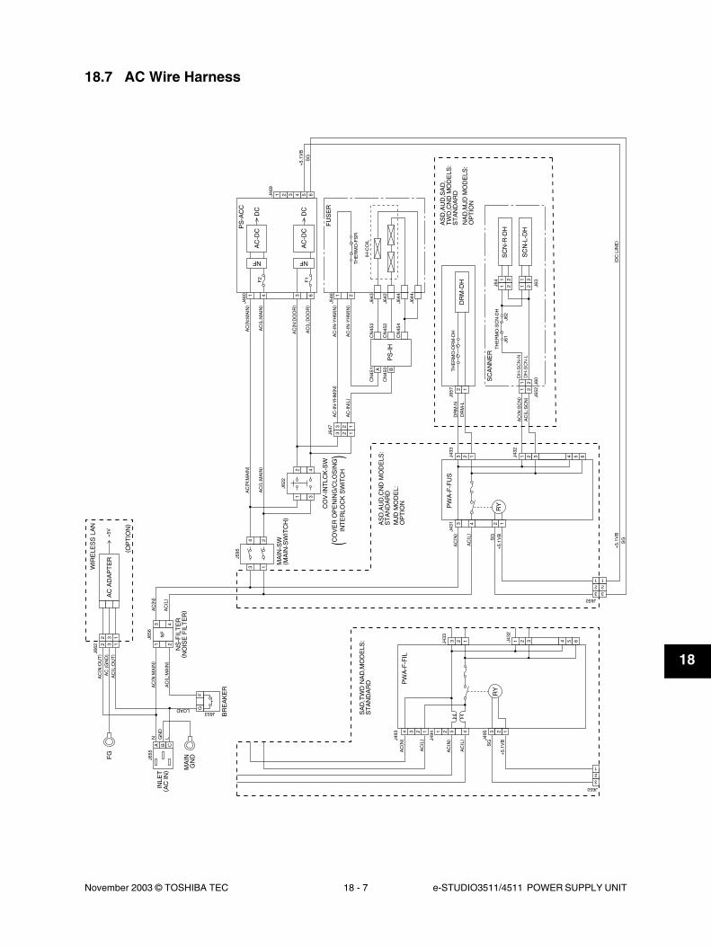
November 2003 © TOSHIBA TEC 18 - 7 e-STUDIO3511/4511 POWER SUPPLY UNIT
18
18.7 AC Wire Harness
1 21 2
1 21 2
RY
PW
A-F
-FIL
SC
AN
NE
RT
HE
RM
O-S
CN
-DH
11
22
SC
N-L
-DH
SC
N-R
-DH
123
123
J652
J657
J433
J595
J656
J662
J655
J653
J622
J431
J432
J60
J63
J64
J61
J62
AC
( N:S
CN
)
SG
+5.
1VB
AC
( N)
AC
( L)
AC
( L:S
CN
)
TH
ER
MO
-DR
M-D
H
TH
ER
MO
-FS
R
+5.
1VB
SG
+5.
1VB
SG
IH-C
OIL
PS
-AC
C
FU
SE
R
PW
A-F
-FU
S
MA
IN-S
W( M
AIN
-SW
ITC
H)
NS
-FIL
TE
R( N
OIS
E F
ILT
ER
)
BR
EA
KE
R
INLE
T( A
C IN
) MA
ING
NDFG
CO
V-I
NT
LCK
-SW
AS
D,A
UD
,SA
D,
TW
D,C
ND
MO
DE
LS:
ST
AN
DA
RD
NA
D,M
JD M
OD
ELS
:O
PT
ION
2 1
DR
M-N
( DC
LIN
E)
DR
M-L
AC
(N: M
AIN
)
AC
( N:O
UT
)
AC
(G
ND
)A
C( L
:OU
T)
AC
(L: M
AIN
)
AC
( N:M
AIN
)
AC
( L:M
AIN
)
AC
( N)
AC
( L)
AC
( N:M
AIN
)
AC
( L:M
AIN
)
AC
( N:D
OO
R)
AC
( L:D
OO
R)
AC
-IN
-YH
M( N
)
AC
-IN
-YH
M( N
)
AC
-IN
-YH
M( N
)
AC
-IN
( L)
J650
+5V
AC
AD
AP
TE
R
DR
M-D
H
PS
-IH
AC
-DC
DC
NF
AC
-DC
DC
NF
4 5 61
1
2
2
33
4 2
3 1
2 4
1 23 6654321
1 4
1 3
2 1
3 4
RY
J469
J647
J460
J546
J643
J642
J644
J644
CN
453
F1
F2
CN
452
CN
451
CN
450
CN
454
3
A B
1
32
2 1
3 13
22 1
3A
GF
B C4
1 2
NF
N GN
DL
( OP
TIO
N)
WIR
ELE
SS
LA
N
(CO
VE
R O
PE
NIN
G/C
LOS
ING)
INT
ER
LOC
K S
WIT
CH
DH
-SC
N-L
DH
-SC
N-N
AS
D,A
UD
,CN
D M
OD
ELS
:S
TA
ND
AR
DM
JD M
OD
EL:
OP
TIO
N
SA
D,T
WD
NA
D,M
OD
ELS
:S
TA
ND
AR
D
123
J650
J494
1234
J493
AC
( N)
AC
( L)
SG
13 2
J495
+5.
1VB
3 4
AC
( N)
AC
( L)
21J4
33
J432
4 5 61 2 33 2 1
LOAD

e-STUDIO3511/4511 POWER SUPPLY UNIT 18 - 8 November 2003 © TOSHIBA TEC
18
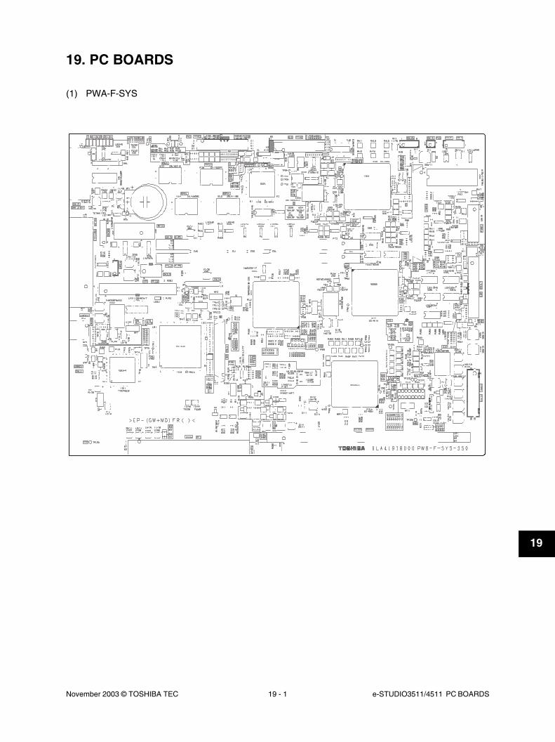
November 2003 © TOSHIBA TEC 19 - 1 e-STUDIO3511/4511 PC BOARDS
19
19. PC BOARDS
(1) PWA-F-SYS

e-STUDIO3511/4511 PC BOARDS 19 - 2 November 2003 © TOSHIBA TEC
19
(2) PWA-F-LGC

November 2003 © TOSHIBA TEC 19 - 3 e-STUDIO3511/4511 PC BOARDS
19
(3) PWA-F-SLG
(4) PWA-F-CCD
(5) PWA-F-SDV

e-STUDIO3511/4511 PC BOARDS 19 - 4 November 2003 © TOSHIBA TEC
19
(7) PWA-F-CCL
(6) PWA-F-DRV
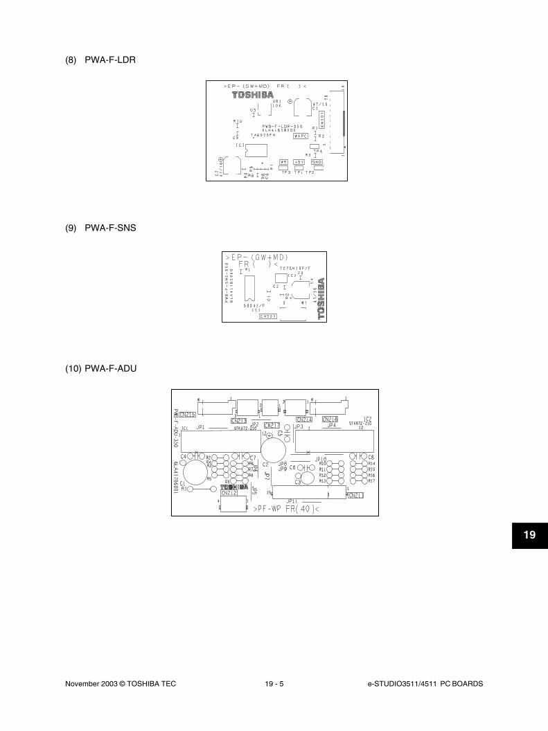
November 2003 © TOSHIBA TEC 19 - 5 e-STUDIO3511/4511 PC BOARDS
19
(8) PWA-F-LDR
(9) PWA-F-SNS
(10) PWA-F-ADU

e-STUDIO3511/4511 PC BOARDS 19 - 6 November 2003 © TOSHIBA TEC
19
(11) PWA-F-DSP
(12) PWA-F-KEY

November 2003 © TOSHIBA TEC 19 - 7 e-STUDIO3511/4511 PC BOARDS
19
(13) PWA-F-FIL
(* NAD/SAD/TWD models: Standard)
(14) PWA-F-FUS
(* ASD/AUD/CND models: Standard, MJD model: Option)

e-STUDIO3511/4511 PC BOARDS 19 - 8 November 2003 © TOSHIBA TEC
19


1-1, KANDA NISHIKI-CHO, CHIYODA-KU, TOKYO, 101-8442 JAPAN


