
1
Towards an affordable Cost of Ownership for EUVL
Melissa ShellPrincipal Engineer & Program Manager, EUVL ResearchComponents ResearchOctober 2006

2006 International EUVL Symposium2006 International EUVL Symposium2
Co-Authors
Robert BristolHeidi CaoManish ChandhokMichael LeesonJeff MacyKevin OrvekAlan Stivers

2006 International EUVL Symposium2006 International EUVL Symposium3
Outline
Technology Development CycleTowards an affordable CoO– CoO evolution during the development cycle
–Technology Implementation Example: 193nm–Key CoO Issues facing EUVL
– Mask Yield/Cost– Scanner Throughput
Extensibility beyond 22nm nodeSummary & Future Work
2006 International EUVL Symposium2006 International EUVL Symposium4
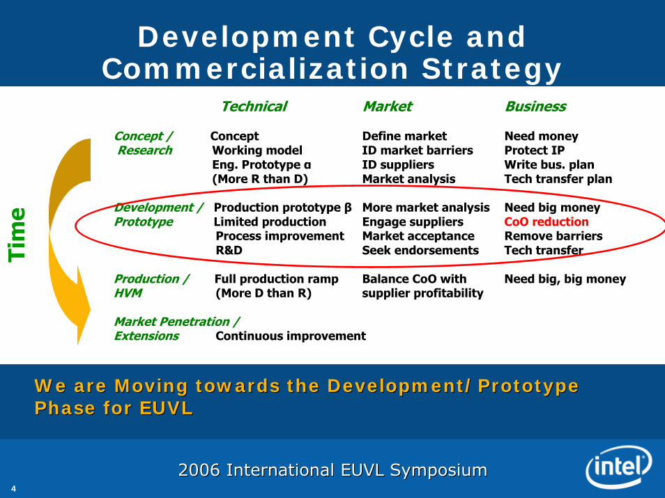
Technical Market Business Concept / Concept Define market Need money Research Working model ID market barriers Protect IP Eng. Prototype α ID suppliers Write bus. plan (More R than D) Market analysis Tech transfer plan Development / Production prototype β More market analysis Need big money Prototype Limited production Engage suppliers CoO reduction Process improvement Market acceptance Remove barriers R&D Seek endorsements Tech transfer Production / Full production ramp Balance CoO with Need big, big money HVM (More D than R) supplier profitability Market Penetration / Extensions Continuous improvement
Tim
eDevelopment Cycle and
Commercialization Strategy
We are Moving towards the Development/Prototype We are Moving towards the Development/Prototype Phase for EUVLPhase for EUVL

2006 International EUVL Symposium2006 International EUVL Symposium5
02468
10121416182022
Q3/
02
Q1/
03
Q3/
03
Q1/
04
Q3/
04
Q1/
05
Q3/
05
Q1/
06
Q3/
06
Q1/
07
Q3/
07
Q1/
08
Q3/
08
Q1/
09
RO
MI V
alue
Source Power Critical Comp. Lifetime Collector Optics LifetimeMask Blank Defectivity Mask Substrate Flatness Reticle ProtectionProjection Optics Lifetime Resist PO Box WFE
Target
Courtesy of Dr. Stefan Wurm, SEMATECH EUV STRATEGY GroupCourtesy of Dr. Stefan Wurm, SEMATECH EUV STRATEGY Group
Rela
tive O
rder
of
Rela
tive O
rder
of
Mag
nit
ud
e I
mp
rovem
en
t M
ag
nit
ud
e I
mp
rovem
en
t R
eq
uir
ed
Req
uir
ed
Concept/Research Phase of EUVLFocused primarily on External Research activitiesFocused primarily on External Research activities
Some internal Intel work on Alpha tool (MET)Some internal Intel work on Alpha tool (MET)
Sufficient Technical Progress is being made industrySufficient Technical Progress is being made industry--wide on many key items that drive COOwide on many key items that drive COO

2006 International EUVL Symposium2006 International EUVL Symposium6
Development/Prototype Phase of EUVL
Main focus of Intel activity shifting to internal work
Will start out with prototype / beta tools, initial resists and masks• Process Latitudes• Particle defects over mask lifetime (shipping and
in-fab use)• OPC (flare) requirements
Tools, resists, mask components evolve over time during this phase• Yields• Pilot Line prototype
193nm Technology example covered in next slides

2006 International EUVL Symposium2006 International EUVL Symposium7
Outline
Technology Development CycleTowards an affordable CoO– CoO evolution during the development cycle
–Technology Implementation Example: 193nm–Key CoO Issues facing EUVL
– Mask Yield/Cost– Scanner Throughput
Extensibility beyond 22nm nodeSummary & Future Work
2006 International EUVL Symposium2006 International EUVL Symposium8
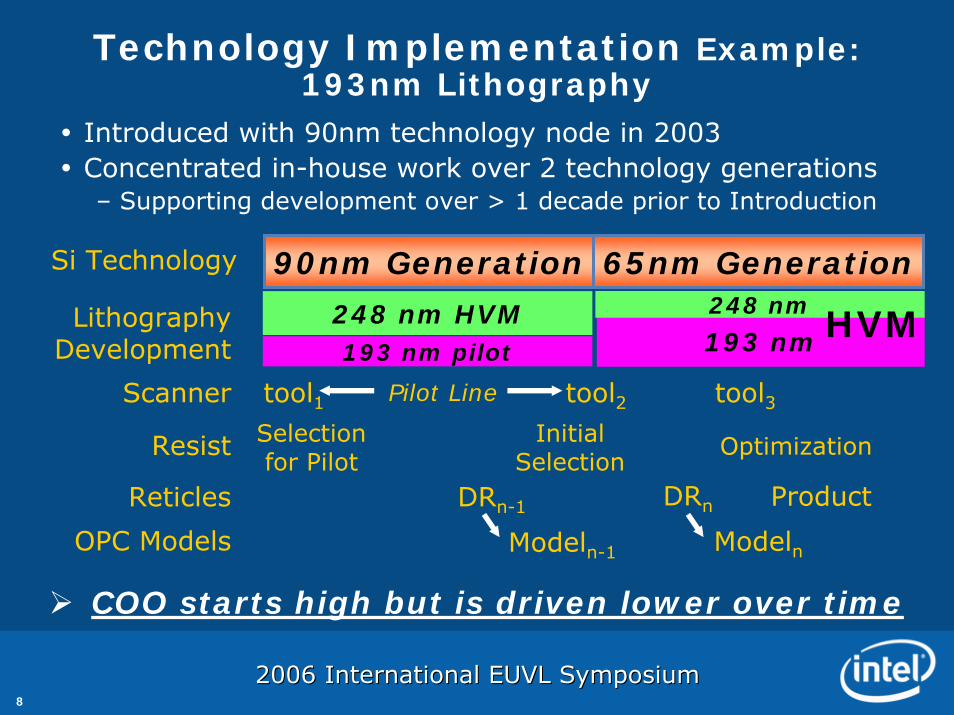
Technology Implementation Example: 193nm Lithography
Introduced with 90nm technology node in 2003Concentrated in-house work over 2 technology generations– Supporting development over > 1 decade prior to Introduction
Lithography Development
Resist OptimizationSelection for Pilot
Initial Selection
Scanner tool1 tool2 tool3Pilot Line
90nm Generation 65nm GenerationSi Technology
Reticles DRn-1 DRn Product
OPC Models ModelnModeln-1
248 nm HVM193 nm193 nm pilot
248 nmHVM
COO starts high but is driven lower over time

2006 International EUVL Symposium2006 International EUVL Symposium9
Lithography COO for two 193nm GenerationsPilot Line thru HVM
Rela
tive L
ith
o C
ost
Rela
tive L
ith
o C
ost
* Actual cost * Actual cost data are data are smoothedsmoothed
CoO is evolutionary – it improves as the technology matures
Technology matures as resources are added (suppliers and users) and tools are deployed
2006 International EUVL Symposium2006 International EUVL Symposium10
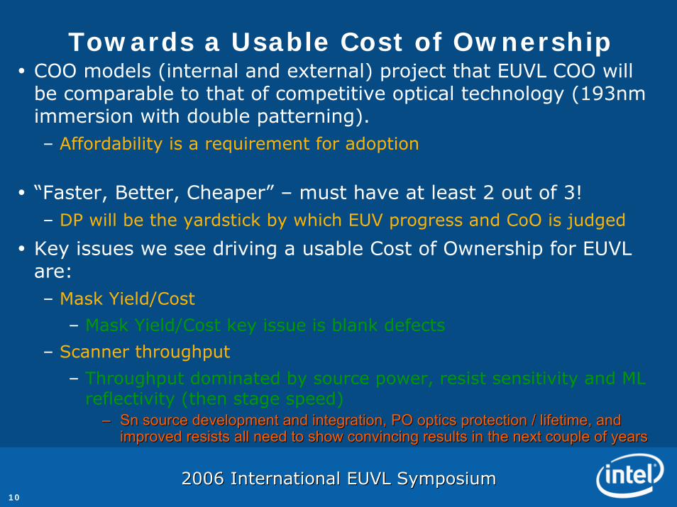
Towards a Usable Cost of OwnershipCOO models (internal and external) project that EUVL COO will be comparable to that of competitive optical technology (193nm immersion with double patterning). – Affordability is a requirement for adoption
“Faster, Better, Cheaper” – must have at least 2 out of 3!– DP will be the yardstick by which EUV progress and CoO is judged
Key issues we see driving a usable Cost of Ownership for EUVL are:– Mask Yield/Cost
– Mask Yield/Cost key issue is blank defects
– Scanner throughput
– Throughput dominated by source power, resist sensitivity and ML reflectivity (then stage speed)
–– SnSn source development and integration, PO optics protection / lifesource development and integration, PO optics protection / lifetime, and time, and improved resists all need to show convincing results in the nextimproved resists all need to show convincing results in the next couple of yearscouple of years

2006 International EUVL Symposium2006 International EUVL Symposium11
Mask Blank Defect ProgressBlank defect data plotted– Normalized to 60nm size – Trend ~100X
improvement in 4 years on best tools
– Need 100X in next 3 years
Major defect sources identified– Substrate defects are
primary Pareto item– Blank suppliers are
investing in improved tools and processes.
Need: Blank defect count <15 at ≥30nm size
1E+0
1E+1
1E+2
1E+3
1E+4
1E+5
1E+6
1E+7
Jul-02
Jul-03
Jul-04
Jul-05
Jul-06
Date
Bla
nk D
efec
t Cou
nt S
cale
d to
60n
m S
ize FS
LTEM
Approx. Goal
Data Envelope

2006 International EUVL Symposium2006 International EUVL Symposium12
EUVL needs less complex OPC compared to 193nm
SRAM cell, isolation layer SRAM cell, metal layer
Printed on IntelPrinted on Intel’’s MET. 110 nm pitch, no OPC, dose = 15 mJ/cm2s MET. 110 nm pitch, no OPC, dose = 15 mJ/cm2

2006 International EUVL Symposium2006 International EUVL Symposium13
Scanner Throughput
Model:Model: Wafer Time (sec) = Wafer Time (sec) = 288*Dose/Power + 20
• Calibrated to 100wph @180W, 10mJ/cm2
• Also shown +-2% reflectance (modifies effective power as R^11)
0
20
40
60
80
100
120
140
0 50 100 150 200 250
Source Power
Waf
ers
per H
our
10mJ/cm2
+/- 2% refl
30mJ/cm2
+/- 2% refl
20mJ/cm2
(W)
2006 International EUVL Symposium2006 International EUVL Symposium14
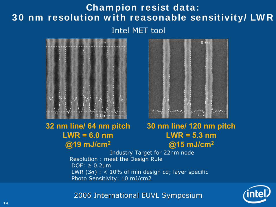
Champion resist data:30 nm resolution with reasonable sensitivity/LWR
30 nm line/ 120 nm pitch LWR = 5.3 nm @15 mJ/cm2
32 nm line/ 64 nm pitch LWR = 6.0 nm @19 mJ/cm2
Intel MET tool
Industry Target for 22nm node Resolution : meet the Design RuleDOF: ≥ 0.2umLWR (3σ) : < 10% of min design cd; layer specificPhoto Sensitivity: 10 mJ/cm2
2006 International EUVL Symposium2006 International EUVL Symposium15
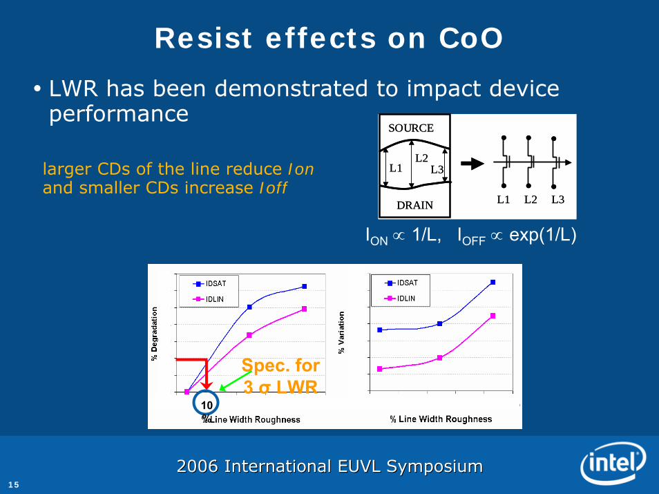
Resist effects on CoO
LWR has been demonstrated to impact device performance
SOURCE
L1L2
L3
DRAIN L1 L2 L3
SOURCE
L1L2
L3
DRAIN L1 L2 L3
ION ∝ 1/L, IOFF ∝ exp(1/L)
larger CDs of the line reduce Ionand smaller CDs increase Ioff
Spec. for 3 σ LWR
10%

2006 International EUVL Symposium2006 International EUVL Symposium16
Resist effects on CoOThe effect of LWR is exasperated by shot noise at small CDs
– The basic effect:- Non-interacting particles arrive at detector at “random”; a variance ~ sqrt(N)- Optics, source on/off, etc control envelop of where/when, but at a particular spot still have variance ~ sqrt(N)
– Shot-noise based LER models - basic approach:– Define a “pixel” in the resist according to smallest length scale resist can
sustain– Count photons, acid, quenchers, etc in pixel at line edge. Overall variance
becomes:
– Resulting LER is proportional to this variance
Novel materials are looking promising to optimize resolution, LWR, and sensitivity simultaneously– Much development is needed, and it may be necessary to slow down
a resist for a given layer
...222 +++= otheracidphotontot σσσσ

2006 International EUVL Symposium2006 International EUVL Symposium17
Effects of Resist Sensitivity on Overall COO
What if we need to back off on sensitivity to achieve required LWR?
Assumes 5 EUV layers out of a total of 30 layers

2006 International EUVL Symposium2006 International EUVL Symposium18
Resist Research continuing to hit targetsCAR: Chemically Amplified ResistsPAGs:
1: EHS Friendly PAGs- Non PFOS (PFAS)2: Polymer-bond PAGs- Anion and Cation 3: Acid efficiency PAGs- High Quantum Efficiency
Resin:1: Molecular Glass Resins- non-polymer type; low Mw resist materials2: PHS based Resins- High/Low Eact protecting groups3: Meth(acrylate) Resins- modified 193nm resin4: Novolac Resins 5: Chain scission Resins- Acid breakable Resins
Non-CAR; Novel developers1. PMMA- Modified??2. Inorganic resists - Photosensitive thin, dense, pore free films3. SCCO2 - Reduced line collapse for high aspect ratios features, plus
LWR reduction4. Out of boxes??
2006 International EUVL Symposium2006 International EUVL Symposium19
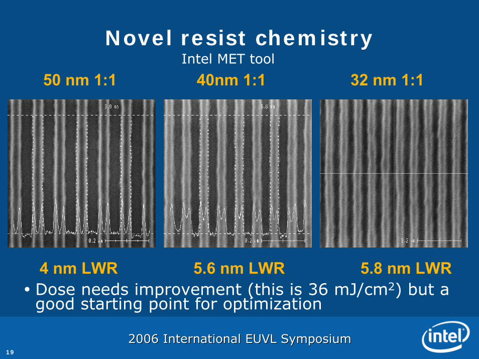
Novel resist chemistry
Dose needs improvement (this is 36 mJ/cm2) but a good starting point for optimization
50 nm 1:1 40nm 1:1 32 nm 1:1
4 nm LWR 5.6 nm LWR 5.8 nm LWR
Intel MET tool

2006 International EUVL Symposium2006 International EUVL Symposium20
Outline
Technology Development CycleTowards an affordable CoO– CoO evolution during the development cycle
–Technology Implementation Example: 193nm–Key CoO Issues facing EUVL
– Mask Yield/Cost– Scanner Throughput
Extensibility beyond 22nm nodeSummary & Future Work
2006 International EUVL Symposium2006 International EUVL Symposium21
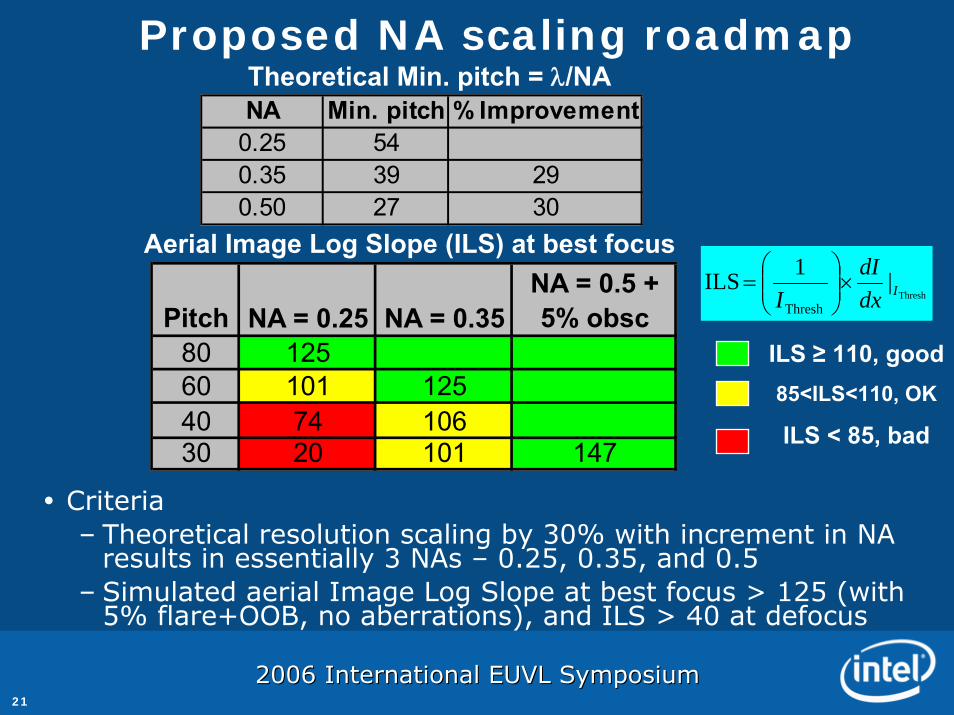
Proposed NA scaling roadmap
Criteria– Theoretical resolution scaling by 30% with increment in NA
results in essentially 3 NAs – 0.25, 0.35, and 0.5– Simulated aerial Image Log Slope at best focus > 125 (with
5% flare+OOB, no aberrations), and ILS > 40 at defocus
NA Min. pitch % Improvement0.25 540.35 39 290.50 27 30
Theoretical Min. pitch = λ/NA
Thresh|1ILS
ThreshIdx
dII
×⎟⎟⎠
⎞⎜⎜⎝
⎛=
Pitch NA = 0.25 NA = 0.35NA = 0.5 + 5% obsc
80 12560 101 12540 74 10630 20 101 147
Aerial Image Log Slope (ILS) at best focus
ILS ≥ 110, good85<ILS<110, OK
ILS < 85, bad
2006 International EUVL Symposium2006 International EUVL Symposium22
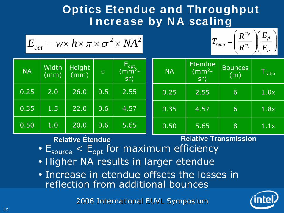
Optics Etendue and Throughput Increase by NA scaling
Esource < Eopt for maximum efficiency Higher NA results in larger etendueIncrease in etendue offsets the losses in reflection from additional bounces
2 2optE w h NAπ σ= × × × ×
NA Width (mm)
Height (mm) σ
2.0 0.5
0.6
0.6
1.5
1.0
Eopt(mm2-
sr)
0.25 26.0 2.55
0.35 22.0 4.57
0.50 20.0 5.65
NAEtendue (mm2-
sr)
Bounces (m) Tratio
0.25 2.55 6 1.0x
0.35 4.57 6 1.8x
0.50 5.65 8 1.1x
m
ratio m
ERTR E
β
α
β
α
⎛ ⎞⎛ ⎞= ⎜ ⎟⎜ ⎟
⎝ ⎠⎝ ⎠
Relative Étendue Relative Transmission
2006 International EUVL Symposium2006 International EUVL Symposium23
SummaryEUVL has transitioned from research into development– This is where CoO reduction efforts ramp up
CoO needs to be similar to or better than alternatives for the technology to be adoptedCoO traditionally starts high and comes down as the technology matures– we need to identify a path to a sustainable CoO– Slowing down the throughput on a layer or two while
working on new resist platforms, while undesirable, is probably tolerable
– EUVL technology is improving, but there is a lot of work ahead

2006 International EUVL Symposium2006 International EUVL Symposium24
Future Work
Transition to HVM requires infrastructure readiness prior to pilot phaseIn the next 3 years we must have:– A reliable, low-debris source with a path to HVM TPT– A capable, but not necessarily optimized resist– Blank defect count <15 at 30nm size or greater– A proven pellicle-less mask strategy– A proven overlay strategy– Proven optics durability– Encouraging Si yield– CoO that is understood and acceptable


