

TRANSISTORS (STAR OF SHOW)Power amplification comes from transistor- other components needed for transistor to work.
Supporting cast (with symbols):a. transformers to get different voltages.b. few other little things not very important.
c.resistors- control currents, divide up voltages as desired.
d. diodes- make AC voltages from transformers into the DC voltages transistors need.
e. capacitors- pass AC while blocking DC. Also store electric charges.
Learning goals: 1) Basic physics of d. and e. General idea how they are used.2) Basic function of transistors as adjustable current gate (voltage controlled resistance) and how this allows amplification of signals.3) NOT expected to learn detailed physics of transistor, will cover briefly.
Gate

diodes- need to convert AC to DC. Transistors insist. Pass current in only one direction. Junction of P doped and N doped semiconductors. anyone understand textbook explanation?
empty
full
pure semiconductor
empty
full
empty
full
p type semiconductor
Si, 4 electrons go intovalence band, just fill B, 3 electrons go into valence band,
leave level unfilled, tinyfraction of total (10^16/10^23 /cm^3)n type semiconductor
Si +tiny fractionboron
Si + tiny fraction Phosphorus
P, 4 electrons go into valence band, 1 extra goes up into cond. band
1/boron atom
How will they conduct? a. all about same.b. pure best, P and N less, c. pure no, P and Nabout same, d. only N conducts, e. only P cond.
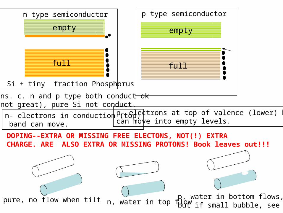
Si + tiny fraction Phosphorus
empty
full
p type semiconductor
empty
full
n type semiconductor
ans. c. n and p type both conduct ok(not great), pure Si not conduct.
DOPING--EXTRA OR MISSING FREE ELECTONS, NOT(!) EXTRA CHARGE. ARE ALSO EXTRA OR MISSING PROTONS! Book leaves out!!!
n- electrons in conduction (top) band can move.
p- electrons at top of valence (lower) bandcan move into empty levels.
pure, no flow when tilt n, water in top flowp, water in bottom flows,but if small bubble, see it.

V+
_
I
Doped semiconductors, add or subtract some charges to allow charges to move.
N type- atoms with extra free electrons- - - - -- - - - -
lower level full
e e e e e e e e
in nearly empty band move easily
V+
_
I+ + + + ++ ++ + +
electrons missing,“holes”, leave room to move easily
DOPING--EXTRA OR MISSING FREE ELECTONS, NOT(!) EXTRA CHARGE. IS ALSO EXTRA OR MISSING PROTONS! Book leaves out!!!

+ + + ++ + + +
- - - - -- - - - -
P- N junction- put together
+ + + ++ + + +
- - - - -- - - - -
electrons diffuse to left(lower energy), fill up holesto annihilate moveablesat border
+ + + + + +
- - - - - - - -
depletion layer- no moveable charges
extra neg’scharge buildup--keeps rest of moveable -’s on right side. Balances energy they get when going down.
full
n type
http://www.colorado.edu/physics/phet/projects/semiconductor/v7/semiconductor.jnlp

+ + + + + +
- - - - - - - -
V
+
_
turn on voltage,what happens?
a. electrons flow from left toright.b. electrons will not flowc. electrons will flow fromright to left

+-+-
V
+
_
turn on voltage, what happens?+s get shoved into depletion-s get shoved into depletion= no more depletion region
moveable charges carry current. I
+++ + + + +++ + + +
- - - - - -- - - - - - --
+ + + + + +
- - - - - - - -
V
-
+
turn on opposite voltage,what happens?
V has to be bigger than 0.6 V toovercome electrostatic barrier from charge.
- - -- - -

+ + + + + +
- - - - - - - -
V
-
+
turn on opposite voltage,what happens?
a. electrons flow from left toright.b. electrons will not flowc. electrons will flow fromright to left

+ + + + + +
- - - - - - -
V
-
+
turn on opposite voltage,what happens?Both +s and -s pulled awayfrom junction. Depletionregion bigger. Currentcan’t flow.
I
So V > 0.6 V in one direction, big current.V in opposite direction, no current.Diode is one-way street for current flow.
-
big pile of negativecharges, no moveablecharges
can also produce light (LED= light emitting diode)- thurs.
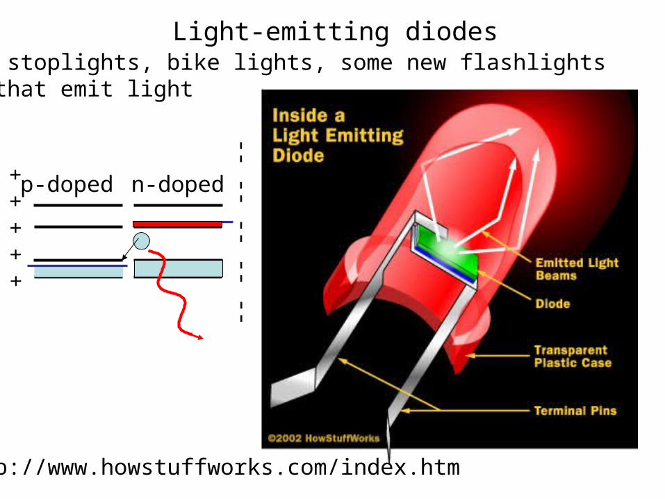
Light-emitting diodesSeen in stoplights, bike lights, some new flashlightsDiodes that emit light
p-doped n-doped + +
+ +
+
-- -- -- -- --
http://www.howstuffworks.com/index.htm

BACK TO THE STAR OF THE SHOW: The Transistor- • like diode, made up of N and P-doped semi-conductors• also has depletion region that controls current flow in transistor• But now we have a separate voltage signal (CD signal) that controls
size of depletion region. We can adjust it up and down, and vary how much current flows through.
tran
sist
or
Transistor Amplifies! A little change in amount of
charge on gate Makes big change in current (through transistor) … varies resistance.
Gate(Valve control)
Gate, change amount of positive charge at gate, control valve.
+
Like water faucet knob, valve for current! Changing signal at Gate … like turning knob … changes current!.
e’sNote: NO direct connection..NO current flow through here!
Lots of excess + charges on gate (voltage)plunger out, current on.
Transistor RESISTANCE IS SMALL.
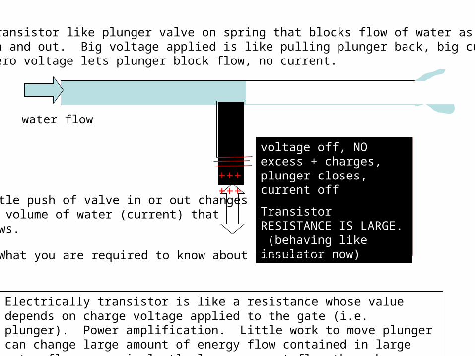
little push of valve in or out changesbig volume of water (current) thatflows.
transistor like plunger valve on spring that blocks flow of water as movedin and out. Big voltage applied is like pulling plunger back, big current,zero voltage lets plunger block flow, no current.
voltage off, NO excess + charges, plunger closes, current off
Transistor RESISTANCE IS LARGE. (behaving like insulator now)
water flow
Electrically transistor is like a resistance whose value depends on charge voltage applied to the gate (i.e. plunger). Power amplification. Little work to move plunger can change large amount of energy flow contained in large water flow or equivalently large current flow through transistor.
What you are required to know about transistors.
++++++
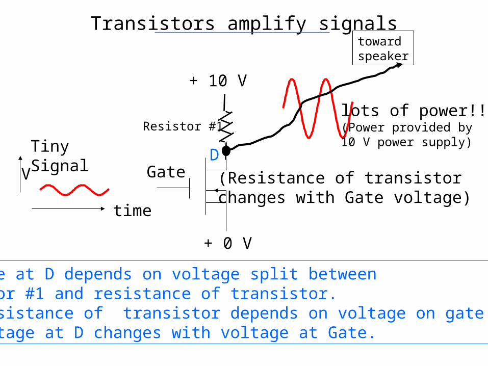
Transistors amplify signals
Gate
+ 10 V
+ 0 V
V
time
Voltage at D depends on voltage split between Resistor #1 and resistance of transistor. But resistance of transistor depends on voltage on gate! So voltage at D changes with voltage at Gate.
Resistor #1lots of power!!(Power provided by10 V power supply)
towardspeaker
(Resistance of transistor changes with Gate voltage)
Tiny Signal
D
GROUND
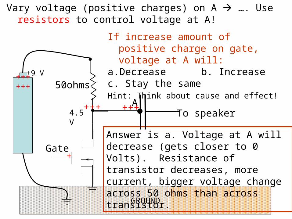
Vary voltage (positive charges) on A …. Use resistors to control voltage at A!
50ohms+9 V
A
++++++
++++++
If increase amount of positive charge on gate, voltage at A will:
a. Decrease b. Increasec. Stay the sameHint: Think about cause and effect!
Gate+
Answer is a. Voltage at A will decrease (gets closer to 0 Volts). Resistance of transistor decreases, more current, bigger voltage change across 50 ohms than across transistor.
To speaker4.5V
short incredibly clear summary of how transistor works in terms of P-N semiconductor junctions…
+ + + + + ++ + + + + +
- - - -- - - -
+ + + + + ++ + + + +
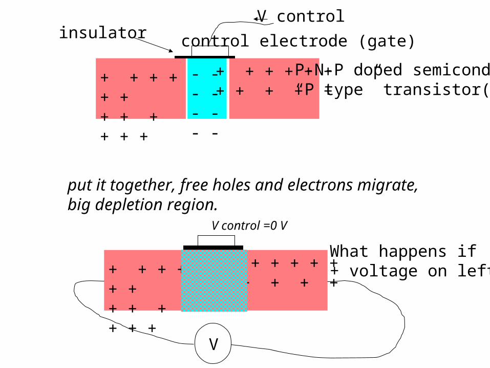
control electrode (gate)
V control
P-N-P doped semicond.“P type” transistor(?!)
insulator
put it together, free holes and electrons migrate, big depletion region.
+ + + + + ++ + + + + +
+ + + + + + + + +
V
V control =0 V
What happens if+ voltage on left?
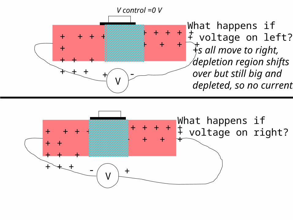
+ + + + + + + + + + +
+ + + + + + + + +
V
V control =0 V
What happens if+ voltage on left?
+ -
+s all move to right,depletion region shiftsover but still big anddepleted, so no current.
+ + + + + ++ + + + + +
+ + + + + + + + +
V
What happens if+ voltage on right?
+-

+ + + + + ++ + + + + +
+ + + + + + + + + + +
V
What happens if+ voltage on right?
+-
Everything moves tothe left, still depletion,no current flow.
v control = 0 V
+ + + + + ++ + + + + +
+ + + + + + + + +
++++
V
V control =+ big voltage What happens big voltage on gate?

+ + + + + ++ + + + + +
+ + + + + + + + +
++++
V
V control =+ big voltage What happens?+s repel +s, so depletionregion gets bigger, no I.
I
What happens if big negative control voltage on gate?

------
V
V control =- big voltage
I
+ + + + + + + ++ + + + + + + +
+ + + + + + + + + + + + +
+s fill in, depletionregion goes away,current flows easilyin either direction.
If moderate negative voltage, just reduce but not remove depletion,a few ++s to carry charge. Less current (i. e. more resistance.)
So amount of current depends on size of negative controlvoltage. If zero or positive no current (like open switch). If big, like closed switch (no resistance).In between, current varies as negative voltage variesbut gives amplification.
But what if want to amplify positive voltages?
++++++
sucked up to -sbut stop at insulator
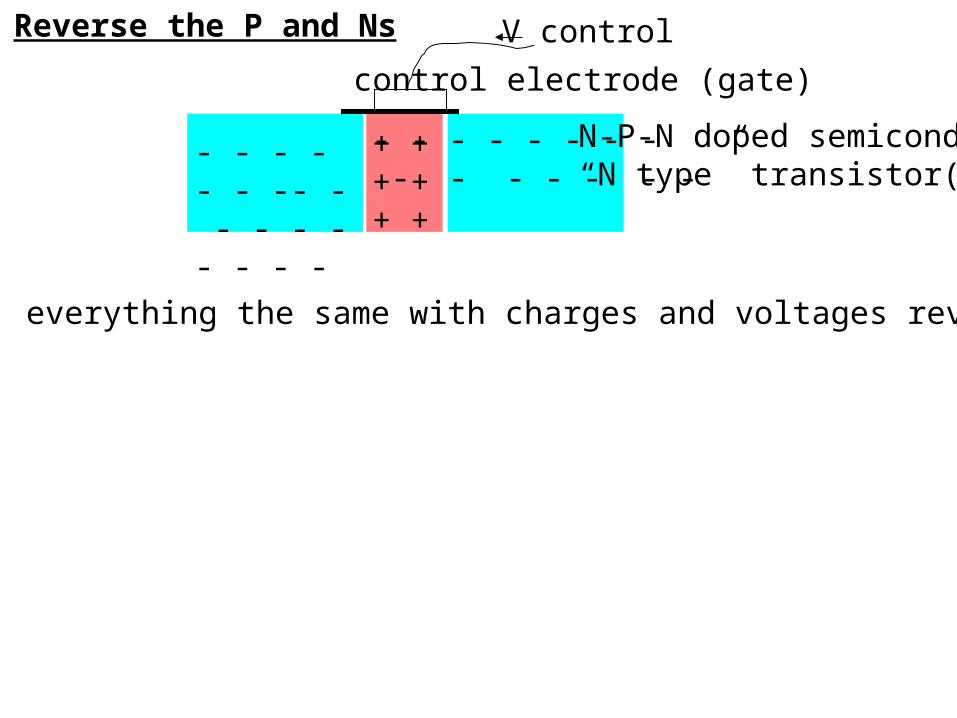
Reverse the P and Ns
- - - - - - -- - - - - - - - - -
+ + + + + +
- - - - - - - - - - - - - - -
control electrode (gate)
V control
N-P-N doped semicond.“N type” transistor(?!)
everything the same with charges and voltages reversed.
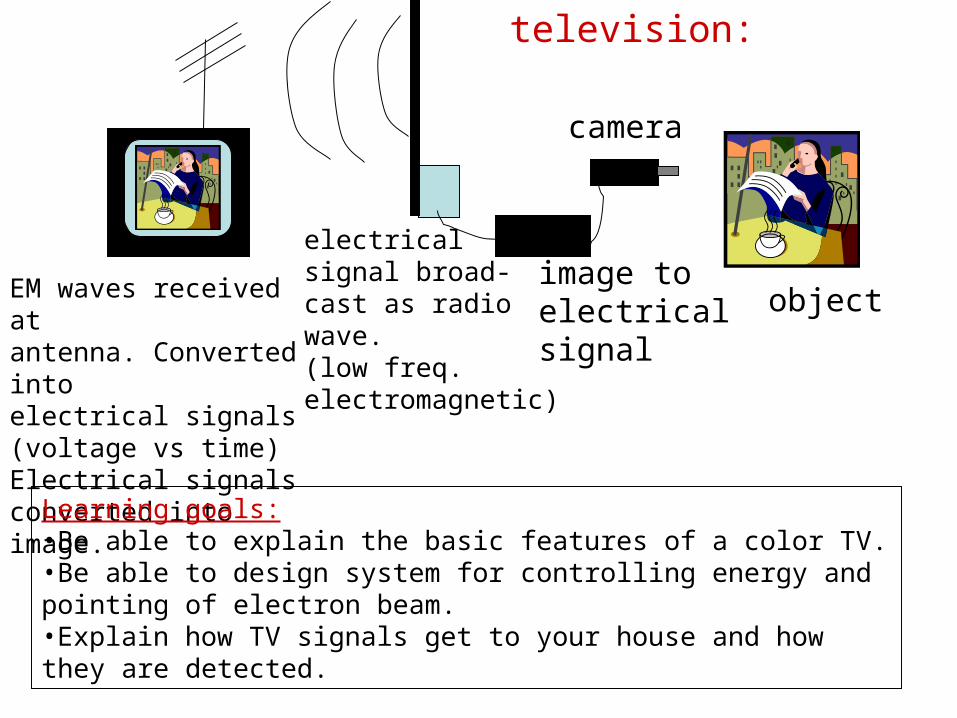
image toelectrical signal
object
camera
electricalsignal broad-cast as radiowave.(low freq. electromagnetic)
EM waves received atantenna. Converted intoelectrical signals (voltage vs time) Electrical signals converted into image.
Learning goals:•Be able to explain the basic features of a color TV.•Be able to design system for controlling energy and pointing of electron beam.•Explain how TV signals get to your house and how they are detected.
television:

Guiding principle of TV: the human eye is crummy.take advantage of this and send as little information as possibleto make viewer think is real color moving picture.
Eye deficiencies:a. fuzzy- leave out almost all detail from TV picture, just use
bunch of dots.b. slow- just flash dots up, then change.c. poor color sense (3 sensors)- just use three colors to trick
into thinking full color range (red, green, and blue).


