
Transparent glass based single electrode mode triboelectric tracking
sensor array
Jinkai Chen, Peng Ding, Ruizheng Pan, Weipeng Xuan, Dapeng Guo, Wuliang Yin and Jikui
Luo
Abstract: Glass based single electrode mode triboelectric generator (SETEG) has been made
and PDMS negative charge material is used to cyclically contact with it under different
contact forces, frequencies and spacers. There will be higher electric output under higher
contact force, frequency and spacer. The SETEG shows a better electric output performance
with a thinner glass positive charge material under lower ambient humidity condition. An
open circuit voltage, short circuit current and power up to 318 V, 8.3 μA and 427 μW has been
obtained with only 5×5 cm contact area. The sensor array wafer is then made with 9 separated
5mm×5mm SETEG on it and the voltage output can easily reach 2 V under ~1 N PDMS
covered stylus touch. A LabVIEW based automatic measure system is built to record,
calculate and display the voltage output of the sensing array under the stylus contact. The
recorded output voltage shows good independence and can easily be calculated to track the
motion of the stylus, demonstrating the great potential of the glass based SETEG to be made
into sensing applications in our daily life.
Keywords: transparent, glass based, sensor array, automatic measure system
1. Introduction
With the rapid development of the Internet of things (IoT), the complementary
energy sources and self-powered sensors are attracting more and more attentions.
There are plenty of potential choices for complementary energy sources, which are
based on piezoelectric[1, 2], pyroelectric[3, 4] and triboelectric[5, 6] effect etc. The
triboelectric generator (TEG) uses the contact of two materials with opposite charge
affinities to convert the mechanical energy into electric energy and it is considered to

be one of the most promising complementary energy sources due to its simpler device
structure, lower cost, easiness for large-scale fabrication and most importantly, the
higher electrical output compared with other microgenerators. Besides, TEG can
generate electric energy through the mostly used three types of contact modes, which
are the vertical contact, lateral slide and single electrode mode. As only one of the
charge material is connected to the circuit, the SETEG is not the best choice for
generator due to its smallest quantity of generated electricity[7]. However, this
structure is more suitable to be used in the daily life as a self-powered sensor because
the other unconnected material can be anything such as rain drop[8], finger[9, 10] and
pavement[11] etc.
Glass has the advantages of high transparency, excellent corrosion and wear
resistance, thermal reliability and hardness etc. It has been widely used in our daily
life from the satellites in the universe to the mobile phones in our hands. For the usage
in the contact mode TEG, it has showed good electrical output and excellent
mechanical reliability in our previous work[12]. But there is no actual practical TEG
application made from glass has been reported.
Here we report a further development of the transparent SETEG tracking sensor
array based on commercially available glass and polydimethylsiloxane (PDMS)
covered touch stylus. And the preliminary test with 5 cm×5 cm glass and PDMS
charge materials shows an open circuit voltage, short circuit current and power up to
318 V, 8.3 μA and 427 μW, respectively. And the following test performed on the
sensor array has a voltage output larger than 2 V with a 5 mm×5mm device size and
~1 N contact force, which can be easily detected by a commercial analog to digital
converter (ADC). The glass based sensor array demonstrates its great potential for the
integration of the enormous existed glass application and the promising newly
developing TEG.
2. Fabrication and experiment setup
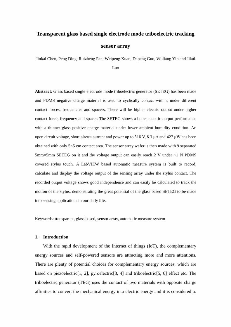
Figure 1 the 3D illustration of the SETEG with the glass and PDMS parts (a) and the sensing array
wafer (b). The sensing array wafer was connected to a central hollowed printed circuit board (PCB)
using conductive tape, showing good optical transparency (c). (d) A stylus with a PDMS covered head
was touching and sliding on the glass side of the sensing array wafer during the test. (e) The voltage
data from 9 independent SETEGs on the sensing array wafer were collected using a DAQ card.
Before fabricating the sensing array wafer, we firstly need to systematically
estimate the performance of the SETEG using glass and PDMS as the charge material.
The complete 5 cm ×5 cm structure with the upper PDMS part and the lower glass
part is shown in Fig. 1(a). The PDMS (184 Silicone Elastomer, Dow corning Co. Ltd.)
solution, which was a mixture of the base PDMS and the crosslinker at a ratio of 10:1
by mass, was spun on the commercially available 1 mm soda lime glass at 1100 rpm
for 10 seconds to obtain a PDMS thin film with a thickness of ~100 μm. Then the
PDMS layer on the glass substrate (the upper PDMS part) was crosslinked on a hot
plate at 100 °C for 25 minutes. The lower glass part consists of a commercially
available soda lime glass with different thicknesses (0.55 mm, 1 mm, 2 mm and 3
mm), a transparent indium tin oxide (ITO) conductive thin layer (750 nm, Resistivity
= 3.525×10⁻⁴ Ω∙cm) and an acrylic protective layer. The ITO layer was deposited on

the soda lime glass by the direct-current reactive magnetron sputtering with 150 W
power, 0.7 Pa pressure and -75 V bias voltage[13]. For a better transparency and
conductivity, the ITO was then annealed using a rapid thermal annealing machine
(RTP-CT100M) at 300 °C for 5 minutes in N2 atmospheric pressure. Finally, the
protective acrylic layer was glued to the ITO layer. These samples were made for the
preliminary test to demonstrate its capability to be used as TEG sensor array. A
dynamic fatigue tester (Popwill Model YPS-1) was utilized to control the cyclic
contact force, frequency and space of two TEG charge pairs, which was the same as
the experiment setup in our previous work[12]. The voltage and current output were
collected using an oscilloscope (Tektronix MDO3022) and a picometer (Keysight
B2981A), respectively.
The 3D illustration of the sensing array wafer (0.55 mm thickness, 5 cm ×5 cm)
with 9 SETEGs (5 mm×5mm) is shown in Fig, (b). The ITO pattern on the glass
wafer was fabricated using the conventional ultraviolet light photolithography and
lift-off process and it was then deposited and annealed using the same conditions
mentioned above. The central 9 squares of the ITO pattern were the electrodes for the
9 SETEGs, and the relatively smaller 9 squares around were designed for the
connection of the sensor array wafer and the PCB using the conductive tape, which
was shown in Fig. 1(c). The good transparency of ITO and glass structure has been
reported in our previous work[12]. The PCB was designed to have a hollowed square
window to demonstrate the good optical transparency of the sensor array wafer, the
image on the computer screen can be seen clearly with the sensor array wafer on it.
Fig. 1(d) shows the test situation of the sensor array, a stylus with a PDMS
covered head was touching or sliding on the front side (glass side) of the sensing array
wafer and Fig. 1(b) is captured exactly from the back side (ITO side) of the sensing
array wafer. The voltage signals are collected using a data acquisition (DAQ) USB
card (Adlink USB 1902) connected to the computer, as shown in Fig. 1(e). A
self-developed LabVIEW program is then used to calculate the voltage data from 9
independent SETEGs to display the real-time voltage curve and tracking animation on
the computer screen.
3. Results and discussion
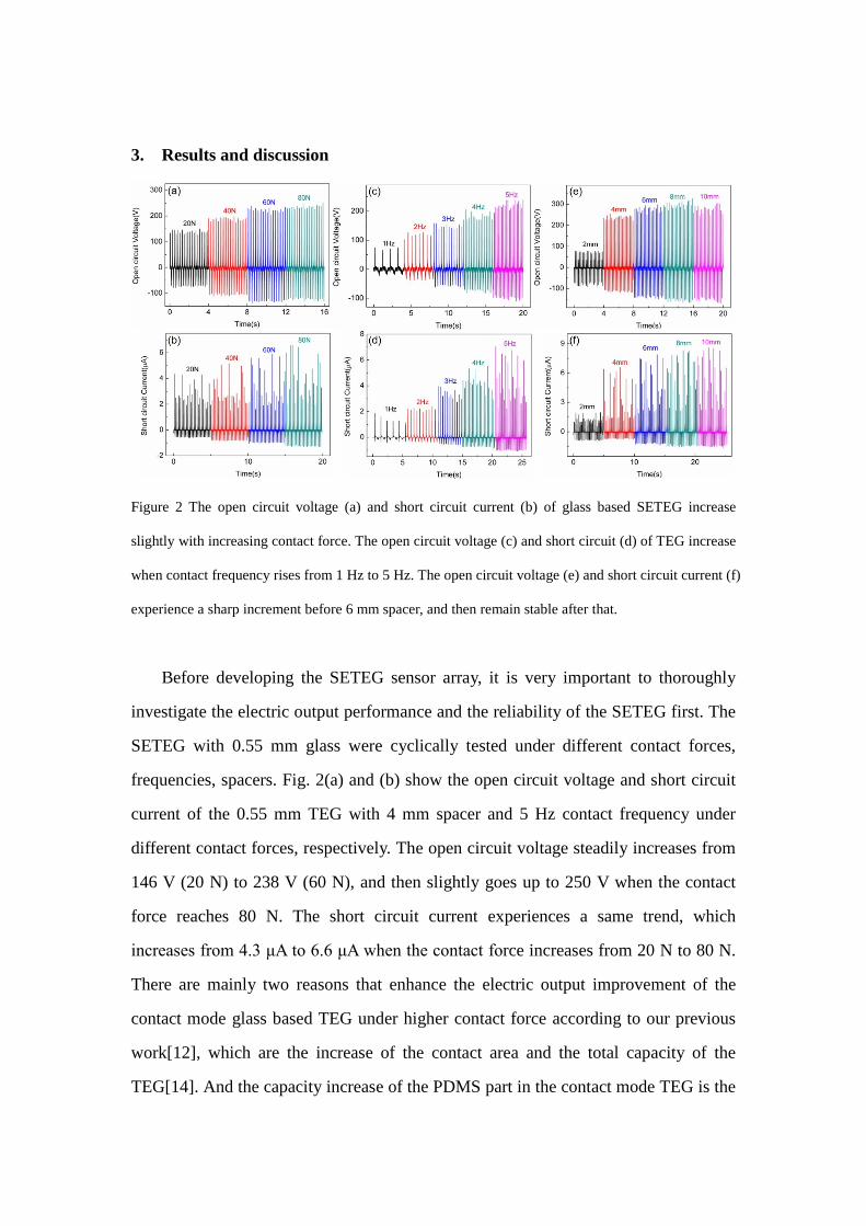
Figure 2 The open circuit voltage (a) and short circuit current (b) of glass based SETEG increase
slightly with increasing contact force. The open circuit voltage (c) and short circuit (d) of TEG increase
when contact frequency rises from 1 Hz to 5 Hz. The open circuit voltage (e) and short circuit current (f)
experience a sharp increment before 6 mm spacer, and then remain stable after that.
Before developing the SETEG sensor array, it is very important to thoroughly
investigate the electric output performance and the reliability of the SETEG first. The
SETEG with 0.55 mm glass were cyclically tested under different contact forces,
frequencies, spacers. Fig. 2(a) and (b) show the open circuit voltage and short circuit
current of the 0.55 mm TEG with 4 mm spacer and 5 Hz contact frequency under
different contact forces, respectively. The open circuit voltage steadily increases from
146 V (20 N) to 238 V (60 N), and then slightly goes up to 250 V when the contact
force reaches 80 N. The short circuit current experiences a same trend, which
increases from 4.3 μA to 6.6 μA when the contact force increases from 20 N to 80 N.
There are mainly two reasons that enhance the electric output improvement of the
contact mode glass based TEG under higher contact force according to our previous
work[12], which are the increase of the contact area and the total capacity of the
TEG[14]. And the capacity increase of the PDMS part in the contact mode TEG is the

primary reason that results in the total capacity increase of the TEG, because glass is a
rigid material and higher contact force will only compress the PDMS triboelectric
layer, leading to a smaller thickness, which means a larger flat panel capacity of the
PDMS part. For SETEG, the PDMS part has not electrically linked to the TEG, so the
total capacity of the TEG actually remains almost unchanged. Only the increasing
contact area is enhancing the electric output performance under higher contact force,
and that’s the reason why the electric output improvement of the glass based SETEG
under higher contact force was not as good as that of glass based contact mode
TEG[12]. The open circuit voltage and short circuit current with 50 N contact force
and 4 mm spacer under different contact frequencies are shown in Fig. 2(c) and (d).
The open circuit voltage gradually increases from 74 V to 238 V when the frequency
increases from 1 Hz to 5 Hz, while the short circuit current shows the same trend,
gradually increasing from 1.9 μA (1 Hz) to 7 μA (5 Hz). The rising trend of the
electric output can be attributed to the rapider contact under higher frequency, which
leads to a faster induction and movement of charges. Fig. 2(e) and (f) illustrate the
open circuit voltage and short circuit current with 50 N contact force and 5 Hz contact
frequency under different spacers, respectively. It is clear from these two figures that
the electric output saturate when the spacer is larger than 8 mm. The open circuit
voltage and short circuit current is 75 V and 1.9 μA at 2 mm spacer, followed by a
sharp increase to 254 V and 6.6 μA when the spacer gets to 4 mm, then slightly
increase to 318 V and 8.3 μA at 8 mm spacer. As the contact frequency is the same for
different spacer conditions, higher spacer means higher relative velocity of the PDMS
and glass triboelectric layers, which will lead to a faster charge transferring speed thus
a better electric output performance.

Figure 3 (a) open circuit voltage, (b) short circuit current and (c) power of SETEG with different glass
thicknesses (0.55 mm, 1 mm, 2 mm and 3 mm), decreasing with the increasing glass thickness. (d)
open circuit voltage, (e) short circuit current and (f) power under different humidity levels, decreasing
with the increasing humidity.
Besides testing the SETEG performance under different contact conditions, we
have also measured the electric output performance of the glass based SETEG with
different environment humidities and thicknesses of glass. Fig. 3(a), (b) and (c) show
the open circuit voltage, short circuit current and power of the SETEG with 4
different glass thicknesses under 50 N contact force, 5 Hz contact frequency and 4
mm spacer, respectively. The open circuit voltage gradually decreases from 238 V to
135 V when the glass thickness increases from 0.55 mm to 3 mm. The short circuit
shows a same trend, which decreases from 7.1 μA to 3.5 μA while the glass thickness
increases from 0.55 mm to 3 mm. It can be seen clearly from Fig. 3(c) that the peak
power is close when the glass thickness is less than 1 mm, which is 359.1 μW and
331.7 μW for 0.55 mm and 1 mm glass thickness, respectively. With a further increase
of the glass thickness, the peak power declines dramatically to 159.3 μW when the
glass thickness reaches 2 mm. And then the decrease trend becomes smooth again,
and the peak power of the TEG with 3 mm glass slightly drops to 149.1 μW. The
downtrend of the peak power might be attributed to the larger portion of charges lost

during the propagation from the surface of a thicker glass to the ITO electrode. The
glass based SETEG is designed to be used in our daily life and as the previously
works reported, higher humidity level will lead to the electric output deterioration due
to the inducted charge leakage on the surface of the triboelectric material[15], so the
measurement of the open circuit voltage, short circuit current and power under
different humidities, which have been shown in Fig. 3(d), (e) and (f) respectively, is
extremely important. The open circuit voltage decreases from 282 V at 38 % to 61 V
at 73 %, and the short circuit current declines from 6.6 μA to 1.6 μA when the
humidity increases from 38 % to 73 %. For the peak power, it is only 21.4 μW at 73 %
humidity, and dramatically increases to 427 μW at 38 %. The power output at high
humidity level is undoubted too small for the energy harvesting applications, but it is
sufficient for the sensing applications as the commercial ADC can easily measure
voltage signal in millivolt scale.
Figure 4 The open circuit voltage of the SETEG with 0.55 mm glass cyclically test for more than
10000 periods, demonstration its excellent stability.
The stability is one of the most important criterions to decide if the sensors are
good or not. Fig. 4 is the open circuit voltage of a SETEG with a 0.55 mm glass
cyclically tested for more than 10000 periods. The initially tested open circuit voltage
is 322 V, and it slightly rises to 350 V after 3000 periods’ contact. After that, the open
circuit voltage keeps stable until the end of the test. The increment of the open circuit
voltage can be explained by the better contact of the PDMS and glass, which leads to

a larger contact area.
Figure 5 (a) 3D illustration captured from front side (glass side) of the sensing array wafer and the 9
separated SETEG sensors have been numbered from Port 1 to Port 9. (b) DAQ device collected voltage
output of Port 1. The negative and positive voltage is generated when the stylus presses on and release
from the glass surface, respectively.
Figure 6 stacked voltage pictures for 9 ports touch independently (a) and being slided with Z type (b)
by a stylus, showing a good independence of these 9 SETEG sensors.
All the experiments above have demonstrated the feasibility of using the
commercial glass to make the sensor array application. Fig. 5(a) is the 3D illustration
captured from the front side (glass side) of the sensor array wafer. There are 9

independent SETEG sensors made in 1 complete glass wafer and they have been
numbered from Port 1 to 9. After the fabrication of the sensor array, an automatic
measure system is built to record, calculate and display the voltage output of the
sensing array under the contacting of the PDMS covered stylus. Fig. 5(b) shows the
voltage output of port 1 under the stylus touching recorded by the DAQ. A negative
and positive voltage is generated when the stylus presses on and releases from the
glass surface, respectively. The generated voltage is not as large as the results tested
under the dynamic fatigue tester as the contact force of stylus is very small force (~1
N), but it is large enough for a commercial DAQ to collect.
Figure 7 Schematic diagram of the multi-channel DAQ device collecting data from 9 independent TEG
sensors. The over-large input impedance of SETEG will lead to a ghosting effect.
The stack illustrations of 9 ports contacted one by one is shown in Fig. 6(a). Fig.
6(b) shows the voltage output when the stylus sliding on the sensing array with a Z
type. It moves with a sequence of Port 1, Port 2, Port 3, Port 3, Port 5 Port 7, Port 7,
Port 8 and Port 9. It is clear that when one port is being touched, the voltage signal
can also be generated from other ports. For example, when port 9 is touched around
30s in Fig. 6(a), there is a small peak also occurred in Port 1. This phenomenon can be

called as ghosting effect and explained using the measure principal of a commercial
DAQ device. As shown in Fig. 7, for a commercial economic DAQ, it usually only
has one ADC and a multiplexer is used to switch from one channel to another
according to sampling rate when doing a multi-channel measurement, which means
only one channel can be recorded at a time even for multi-channel setup. When the
multi-channel analog signals come into the DAQ device, the multiplexer will first
choose one of this signals and then let it charge the capacitor C in the front of the
ADC to reach the voltage of the source analog signal. The time used for the capacitor
charging from the initial voltage to the source signal voltage is called the setting time.
After the convert of the first channel finished, the multiplexer will switch to next
channel, and the capacitor C starts to charge from the voltage of the previous channel
to the voltage of the channel connected. For common analog source, the DAQ device
works perfectly, but it is well known that TEG has a very large input impedance (R1 to
R9 as shown in Fig. 7) at tens or even hundreds of MΩ, which means it will take much
more time for TEG source to charge or discharge the capacitor C (higher setting time).
For instance, after the voltage convert of Port 9, the capacitor C has a high voltage
and when the multiplexer switches to Port 1, as the source analog signal of Port 1 is 0
V, the capacitor C will tend to discharge to 0 voltage, but the high input impedance
leads to a longer setting time, which means it can not be discharged to 0 V before the
next channel switching action comes and the ADC records a voltage higher than 0 V
for Port 1. The ghosting effect can be weakened by using a DAQ device with multiple
ADCs or just set the sampling rate as low as possible for the capacitor C having
enough time to charge or discharge to source voltage. Here we set the sampling rate (~
250 ms per point or 4 Hz) lower for weakening the ghosting effect, which can be
nearly neglected as shown in Fig. 6(a) and (b), showing a good independence of these
9 TEG ports.

Figure 8 Voltage output under 9 independent touch (a) and Z type sliding (b), showing the capability of
the sensing array to track motion on the glass surface.
Figure 9 LabVIEW Graphic interface is used to display the real-time voltage output (left) and the trace
(right) of the moving stylus.
The contact sequence and voltage amplitude can be seen more clearly in Fig. 8(a)
and (b), which are the voltage output under 9 independent touch and Z type sliding,
respectively. The peak voltage output in Fig. 8(a) is 2.03 V, 2.81 V, 2.99 V, 2.33 V,
3.46 V, 2.55 V, 3.66 V, 2.45 V and 4.53 V for Port 1 to 9, respectively. The voltage
outputs are not the same because human hand controlled stylus touching have
different contact conditions every time, but all the voltage amplitudes of 9 ports are
large enough for any commercial DAQ devices to collect. The move sequence can be
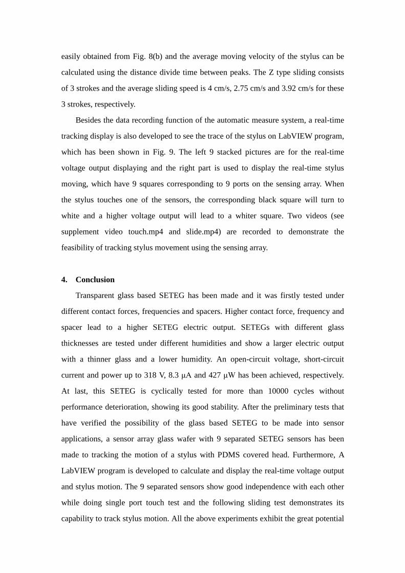
easily obtained from Fig. 8(b) and the average moving velocity of the stylus can be
calculated using the distance divide time between peaks. The Z type sliding consists
of 3 strokes and the average sliding speed is 4 cm/s, 2.75 cm/s and 3.92 cm/s for these
3 strokes, respectively.
Besides the data recording function of the automatic measure system, a real-time
tracking display is also developed to see the trace of the stylus on LabVIEW program,
which has been shown in Fig. 9. The left 9 stacked pictures are for the real-time
voltage output displaying and the right part is used to display the real-time stylus
moving, which have 9 squares corresponding to 9 ports on the sensing array. When
the stylus touches one of the sensors, the corresponding black square will turn to
white and a higher voltage output will lead to a whiter square. Two videos (see
supplement video touch.mp4 and slide.mp4) are recorded to demonstrate the
feasibility of tracking stylus movement using the sensing array.
4. Conclusion
Transparent glass based SETEG has been made and it was firstly tested under
different contact forces, frequencies and spacers. Higher contact force, frequency and
spacer lead to a higher SETEG electric output. SETEGs with different glass
thicknesses are tested under different humidities and show a larger electric output
with a thinner glass and a lower humidity. An open-circuit voltage, short-circuit
current and power up to 318 V, 8.3 μA and 427 μW has been achieved, respectively.
At last, this SETEG is cyclically tested for more than 10000 cycles without
performance deterioration, showing its good stability. After the preliminary tests that
have verified the possibility of the glass based SETEG to be made into sensor
applications, a sensor array glass wafer with 9 separated SETEG sensors has been
made to tracking the motion of a stylus with PDMS covered head. Furthermore, A
LabVIEW program is developed to calculate and display the real-time voltage output
and stylus motion. The 9 separated sensors show good independence with each other
while doing single port touch test and the following sliding test demonstrates its
capability to track stylus motion. All the above experiments exhibit the great potential

of the glass based SETEG to be utilized in our daily life for sensing applications.
Acknowledgement:
References [1] S.R. Anton, H.A. Sodano, Smart Materials & Structures, 16 (2007) R1-R21. [2] P.K. Panda, JMatS, 44 (2009) 5049-5062. [3] S.R. Hunter, N.V. Lavrik, S. Mostafa, S. Rajic, P.G. Datskos, Proc Spie, 8377 (2012). [4] I. Lubomirsky, O. Stafsudd, Rev. Sci. Instrum., 83 (2012). [5] F.R. Fan, Z.Q. Tian, Z.L. Wang, Nano Energy, 1 (2012) 328-334. [6] G. Zhu, C.F. Pan, W.X. Guo, C.Y. Chen, Y.S. Zhou, R.M. Yu, Z.L. Wang, Nano Lett., 12 (2012) 4960-4965. [7] Y.L. Zi, S.M. Niu, J. Wang, Z. Wen, W. Tang, Z.L. Wang, Nat Commun, 6 (2015). [8] Q.J. Liang, X.Q. Yan, X.Q. Liao, Y. Zhang, Nano Energy, 25 (2016) 18-25. [9] Y. Yang, H.L. Zhang, Z.H. Lin, Y.S. Zhou, Q.S. Jing, Y.J. Su, J. Yang, J. Chen, C.G. Hu, Z.L. Wang, Acs Nano, 7 (2013) 9213-9222. [10] Y. Yang, Y.S. Zhou, H.L. Zhang, Y. Liu, S.M. Lee, Z.L. Wang, Adv. Mater., 25 (2013) 6594-6601. [11] Y.C. Mao, D.L. Geng, E.J. Liang, X.D. Wang, Nano Energy, 15 (2015) 227-234. [12] J. Chen, H. Guo, P. Ding, R. Pan, W. Wang, W. Xuan, X. Wang, H. Jin, S. Dong, J. Luo, Nano Energy, 30 (2016) 235-241. [13] J. Chen, X. He, W. Wang, W. Xuan, J. Zhou, X. Wang, S.R. Dong, S. Garner, P. Cimo, J.K. Luo, J Mater Chem C, 2 (2014) 9109-9114. [14] X.M. He, H.Y. Guo, X.L. Yue, J. Gao, Y. Xia, C.G. Hu, Nanoscale, 7 (2015) 1896-1903. [15] L.S. McCarty, G.M. Whitesides, Angew Chem Int Edit, 47 (2008) 2188-2207.


