

UNIVERSITY OF MINNESOTA
This is to certify that I have examined this copy of a doctoral dissertation by
Ahmet Serdar Sezen
and have found that it is complete and satisfactory in all respects, and that any and all revisions required by the final
examining committee have been made.
Bradley J. Nelson Rajesh Rajamani
__________________________ __________________________ Signature of Faculty Co-Adviser Signature of Faculty Co-Adviser
___________________________________________ Date
GRADUATE SCHOOL

Passive Wireless Sensing Strategies for High Frequency Biomedical Sensing Applications
A DISSERTATION SUBMITTED TO THE FACUTY OF THE GRADUATE SCHOOL
OF THE UNIVERSITY OF MINNESOTA BY
Ahmet Serdar Sezen
IN PARTIAL FULFILLMENT OF THE REQUIREMENTS FOR THE DEGREE OF
DOCTOR OF PHILOSOPHY
Bradley J. Nelson, Adviser Rajesh Rajamani, Adviser
December 2006

© Ahmet Serdar Sezen, December 2006

iii
ABSTRACT
Passive wireless operation is desirable in applications where untethered and maintenance-
free operation is more critical than long distance communication. Unlike the active
devices, passive wireless sensors do not require on-board batteries. Therefore they are
less complicated, smaller, and cheaper and they require no maintenance resulting in
unlimited lifespan. Passive wireless telemetry (PWT) is desirable for a variety of
applications from biomedical implants, to “place and forget” type applications such as
structural health monitoring, food quality monitoring or sensors for high temperature
environments. In biomedical implants the advantages of PWT include the elimination of
complications associated with battery replacement and their small size. The current state
of PWT methods lack the capability of high frequency measurements for sensors that
operate at higher frequencies such as acoustic transducers. This project introduces for the
first time a passive wireless telemetry system capable of high frequency readout with a
specific focus on acoustic sensors for biomedical monitoring applications.
The first method, based on continuous monitoring and demodulation of the RF carrier
signal, utilizes inductive coupling. A telemetry system based on I-Q demodulation and
mutual impedance detection has been developed. This interrogation strategy is further
improved by development of innovative algorithms to improve sensor performance by
eliminating the mutual coupling term from the system of equations. A second method of
passive wireless telemetry, the SAW-IDT based telemetry has also been investigated for
high-frequency compatibility A novel SAW-IDT MEMS microphone integration method
has been described based on P-matrix formulation and acoustic coupling. By using the
unique characteristics of pulse-echo type modulation in SAW devices, it was possible to
retrieve the high frequency data without any need for calibration.
Both approaches to high frequency passive wireless telemetry have been successfully
implemented and experimentally verified to detect high frequency capacitive changes in
batteryless untethered operation.

iv
The integration of MEMS and PWT permits ultra-miniaturization of passive sensor
packages via the elimination or partial-reduction of assembly processes. There are only
few examples of MEMS-PWT integration in literature typically due to the relatively low
telemetry distances and low quality factors associated with the sensors. This project also
includes the design and implementation of a novel surface micromachining strategy
specifically designed to create high sensitivity capacitive membrane based MEMS
sensors with low series resistance suitable for passive wireless telemetry integration. The
low temperature compliant post-CMOS compatible fabrication scheme employs PECVD
silicon nitride membranes and introduces the concept of sandwiched metallization layer
to increase device sensitivity independent of the membrane thickness and capacitive gap.
Capacitive MEMS sensors with sizes ranging between 30 µm and 800 µm have been
successfully fabricated and tested with the proposed inductive coupling based PWT for
frequencies ranging up to 1 MHz. The capacitance estimation method was used to
determine the high frequency capacitance change of the MEMS sensor wirelessly.

v
TABLE OF CONTENTS
LIST OF TABLES.......................................................................................................viii
LIST OF FIGURES..................................................................................................…ix
1 Introduction …………………………………………………………………….. 1
1.1 Active versus Passive Wireless Sensing …………………..…………… 4
1.2 Approaches to Passive Wireless Communication …………………....... 5
1.2.1 Inductive Coupling for Continuous Wave (CW) Monitoring
Using Mutual Impedance …………………………………………… 7
1.2.2 SAW-IDT Based Passive Wireless Sensing …………..………… 9
1.3 Project Goals and Proposed Contributions …………………............... 10
1.4 Biomedical Applications for Passive Wireless High Frequency Sensors… 11
1.4.1 Passive Wireless Intramuscular Pressure (IMP) Sensors ………. 12
1.4.2 Wireless Microphones for Patient Monitoring Applications ...…. 15
2 Passive Wireless Telemetry Basics ………………………………………………19
2.1 Inductive Coupling: Theory of Operation …………………..…………… 19
2.2 Common Method of Operation for Inductive Coupling Based Telemetry.. 22
2.3 Induction and Radiation Fields ………………..…………..…………… 24
2.4 Telemetry Distance ………………………….……………..…………… 25
2.5 SAW-IDT Based Passive Wireless Sensing Basics …………………… 27
2.5.1 Theory of SAW operation ……………………………………….. 27
2.5.2 Design Considerations for SAW Devices ……………………..….31
3 Proposed Passive Wireless Telemetry For High-Frequency Sensor
Measurements…………………………………………………………………... 33
vi
3.1 Proposed Inductive Coupling Based Continuous Wave Mode Operation.. 33
3.1.1 Description of the Methodology ……………………………….. 33
3.1.2 Mathematical Model of the System …………………………….34
3.2 Straightforward Telemetry Scheme Based on Time Domain System
Model ………………….……………………….……………..……………35
3.3 Development of Novel Algorithms for Inductive Coupling …………… 37
3.3.1 Frequency Domain System Model ………………………………38
3.3.2 Simulations ………………………………………………………38
3.3.3 Frequency-Domain Based Cascaded Filter ………………………44
3.3.4 Modified Circuit Model and the Modified Cascaded Filter ………47
3.4 Proposed SAW-IDT Based Operation with Pulse-Echo Type
Modulation ………………….……………………….……………..……. 49
3.4.1 The Mathematical Model …………….………………………… 49
3.4.2 SAW-IDT Integration for High Frequency Acoustic
Sensors …………………………………………………………… 50
4 MEMS Device Design And Microfabrication ……………..……………………53
4.1 Basic Design Considerations for the Capacitive MEMS Sensor Design…. 53
4.1.1 Selection of the Fabrication Type: Bulk or Surface
Micromachining…………………………………………………….. 54
4.2 Challenges of Fabrication …………..…………..…………..…………… 55
4.3 Selection of the Membrane Material ……….……………..…………..…57
4.4 Selection of the Sacrificial Layer and the Electrode Metal ………………59
4.4.1 Investigation of PECVD SiO2 as Sacrificial Layer ……………….. 59
4.4.2 Investigation of Aluminum Metallization with
Chromium Sacrificial Layer ……………………………………….. 60
4.4.3 Aluminum Sacrificial Layer and Cr-Au Metallization …………. 61
4.5 First Batch of MEMS Acoustic Sensors …………………………………. 62
4.5.1 Design of Membrane Geometry …………………………………. 62
4.5.2 Mask Design for the First Batch of Sensors ………………………64

vii
4.5.3 Fabrication Process for the First Batch of Acoustic Sensors …….66
4.5.4 Fabrication Results for the First Generation of Sensors …………..67
4.6 Second Batch of MEMS Acoustic Sensors ………………………………69
4.6.1 Design of Membrane Geometry for the Second Batch of
Acoustic Sensors …………………………………………………….69
4.6.2 Introduction of the Sandwiched Top Layer Metallization to
Increase Sensitivity ……………………………………………….. 69
4.6.3 Circumferential Clamp Design for Membrane Stabilization …….71
4.6.4 Investigation of membrane corrugation on membrane yield ….…72
4.6.5 Mask Design for the Second Batch of Capacitive MEMS
Sensors ………………………………………………………………73
4.6.6 Fabrication of the Second Batch of Capacitive MEMS Sensors …74
4.7 SAW-IDT Device Design and Fabrication ………………………………76
5 Results……………………………………………………………………………... 79
5.1 Experimental Setup for the Inductive Coupling Scheme……………...…… 79
5.2 Passive Wireless Telemetry with Capacitive MEMS Sensor Integration…. 80
5.2.1 Determination of the RF Telemetry Frequency: Sensitivity
Analysis ………………………………………………………………81
5.2.2 Effect of Telemetry Distance ………….……………………….85
5.2.3 Determination of the Frequency Response of the Capacitive
MEMS Sensor………………………………………………………... 86
5.2.4 Capacitance Estimate by using the Proposed Cascaded Filter ….…87
5.3 Experimental Results by Using the SAW-IDT Pulse-Echo Type
Modulation ………………………………………………………………89
6 Conclusion and Summary of Contributions………………..…………………... 93
Bibliography………………………………………………………………………… 96

viii
LIST OF TABLES
Table 1.1 A comparison of the active-passive and absolute-passive wireless telemetry 7
Table 2.1 Typical waveforms and their properties in piezoelectric substrates ……….. 31
Table 2.2 Properties of the common piezoelectric substrates…………………………. 32
Table 4.1 Description of the photolithography masks for the microfabrication process 65
Table 4.2 Description of the photolithography masks for the microfabrication
process………………………………………………………………………74
Table 4.3 The designed SAW-IDT sensor parameters ……………………………….. 77
Table 5.1 The transceiver and sensor circuit parameters ……………………………... 82

ix
LIST OF FIGURES Figure 1.2 A typical surface acoustic wave device…………………………………… 9
Figure 2.1 The basic circuit model for inductive coupling……………………………. 20
Figure 2.2 The amplitude and phase curves to detect the sensor capacitance change in
common measurement method…………………………………………………... 23
Figure 2.3 A typical SAW device configuration for passive wireless impedance
sensing…………………………………………………………………………… 27
Figure 3.1 Simplified diagram of the proposed telemetry system ……………………. 33
Figure 3.2 A detailed circuit diagram for the inductive coupling operation …………. 35
Figure 3.3 A block diagram of the straightforward solution of the time-domain
system of equations…………………………………………………………….… 36
Figure 3.4 The effect of telemetry frequency on overall sensitivity of the passive
telemetry system…………………………………………………………………. 40
Figure 3.5 The effect of the sensor resistance R2 on wireless telemetry……………… 42
Figure 3.6 The effect of antenna coil inductances on system response ………………. 43
Figure 3.7 Experimental results showing acoustic reflectivity with changing
capacitance and simulated relationship between the acoustic pressure and the
corresponding capacitance……………………………………………………….. 52
Figure 4.1 Membrane design for the first batch of sensors …………………………… 63
Figure 4.2 The resolved problem during the fabrication of the masks………………... 66
Figure 4.3 The fabrication process utilized for the first batch of capacitive sensors ….67
Figure 4.4 The SEM and optical microscope photographs of the fabricated sensors…. 68
Figure 4.5 The membrane failure in the first batch of MEMS sensors ………………..68
Figure 4.6 The sensor capacitance and electrical sensitivity with changing thickness
of membrane material in the capacitive gap……...……………………………… 70
Figure 4.7 The circumferential PECVD SiNx clamp design …………………………. 72
Figure 4.8 The effect of membrane corrugation on membrane yield ………………… 73
Figure 4.9 The fabrication scheme for the second batch of capacitive MEMS
sensors……………………………………….………………………………….. 74
Figure 4.10 Photograph of a successfully released capacitive MEMS sensor.………... 76

x
Figure 4.11 The fabrication process sequence for SAW-IDT sensors ………………. 78
Figure 4.12 The fabricated SAW-IDT sensors ………………………………………. 78
Figure 5.1 The experimental setup for inductive coupling passive wireless telemetry 79
Figure 5.2 The fabricated capacitive MEMS membrane array used in the passive
wireless telemetry experiments…………………………………………………. 81
Figure 5.3 The simulated theoretical sensitivity curve for the telemetry system……. 83
Figure 5.4 The experimental sensitivity curve to determine the RF operation
frequency……………………………………………………………………….. 84
Figure 5.5 The amplitude spectrum of the I signal sampled by the DAC system …… 85
Figure 5.6 The effect of telemetry distance on the demodulated signal strength…….. 86
Figure 5.7 The frequency response of the fabricated 500 µm capacitive membrane
array…………………………………………………………………………….. 87
Figure 5.8 The passive wireless capacitance detection results through the
implementation of the cascaded filter…………………………………………... 88
Figure 5.9 The variation in the network reflection parameter for the SAW-IDT
sensors…………………………………………………………………………... 89
Figure 5.10 Data showing the 400 ns SAW-IDT interrogation pulse and its
reflection………………………………………………………………………... 90
Figure 5.11 Experimental setup for testing the varactor-controlled SAW-IDT sensor 91
Figure 5.12 SAW-IDT telemetry experimental results ……………………………… 92

1
CHAPTER 1
INTRODUCTION
Miniature wireless sensors are being used in a wide range of applications from everyday
household items to advanced biomedical implants. Wireless sensor packages are
generally composed of a sensor and a transceiver unit. The sensor readings can be
retrieved by the transceiver via an optical, electromagnetic or magnetic link. Optical and
infrared operations of wireless sensors are limited by the fact that the sensor and the
transceiver have to “see” each other [Last et al. 2003, Chu et al. 1992, Bilaniuk 1997],
which in turn limits their usage in opaque and isolated environments. Magnetic wireless
actuation is a promising field [Yeşin et al. 2005] whereas sensing in smaller dimensions
has its limitations [Miki and Shimoyama 2003]. Magnetoelastic sensors also use
magnetic coupling in the form of rapidly changing magnetic fields to excite a
magnetoelastic substrate and wirelessly detect the changes in the natural frequency of the
sensor which occur as a consequence of environmental changes. However the detection
methods need bulky coils and the resonant frequency detection methods limit the
bandwidth of the sensors to static measurements [Grimes et al. 2000]. Biocompatibility of
magnetoelastic materials is also yet to be validated. Hence the most versatile, cost
effective and accomplished wireless sensing strategy for miniature sensors is RF
telemetry or electromagnetic coupling in which the transmission frequencies may vary
between kilohertz and millimeter wave range. Throughout this thesis, wireless telemetry
or wireless sensing will refer to the wireless data transfer between a transducer and a
transceiver, where the coupling or signal transfer is achieved through the radio frequency
(RF) portion of the electromagnetic spectrum.
Passive wireless telemetry is desirable in applications where untethered operation is more
critical than long distance communication. Unlike active devices, passive wireless
sensors do not require an on-board power source which is usually in the form of a battery.
As a result they are less complicated, smaller, require no maintenance and are cheaper

2
than active wireless sensors. The passive wireless technology is desirable for a variety of
applications, from biomedical implants, where batteryless operation results in significant
reduction in size and eliminates the need for battery replacement, to “place and forget”
type applications such as structural health monitoring with RFID tags [Watters et al.
2002] or sensors for high temperature environments [Fonseca et al. 2002]. There has been
significant work reported on implantable passive wireless sensors such as a neural sieve
electrode [Akin et al., 1998] and an endovascularly-implantable aneurysm pressure
sensor [Allen 2005]. These devices successfully operate over small distances but they
either have complex on-board circuitry which introduces tissue heating issues, or require
expensive and bulky read-out equipment such as impedance analyzers. Furthermore, the
methods that are currently presented in literature are low in bandwidth and can not be
applied to cases requiring high frequency measurements such as acoustic devices where
the bandwidth of the device can very well exceed the human audible range (> 20 kHz).
Even for measurements that do not need high bandwidth, obtaining the high frequency
components of the sensor signal might be advantageous for it might carry extra
information.
Micro-electro-mechanical systems (MEMS) are miniature mechanical transducers that
share the batch microfabrication techniques of the integrated circuit (IC) manufacturing
technologies. When compared to conventional sensors, MEMS are smaller, cheaper,
generally require less power and are easier to combine with the signal processing
circuitry through integrated pre and/or post-CMOS processing technologies. The
possibility of integrated CMOS electronics minimizes the post-fabrication assembly
steps, reduces the final size and cost of the product even further [Baltes et al. 1996] and
minimizes the effect of noise and other parasitic effects especially in radio frequency
operation [Hill et al. 2003].
The integration of MEMS and passive wireless sensing enables the creation of ultra-
miniature wireless sensors. As a consequence of the simplicity of the passive wireless
sensing strategies, wafer level integration of the sensor and additional IC components

3
might be possible, completely eliminating the need for assembly and associated handling
challenges. In some cases, using passive wireless telemetry enhances MEMS sensor
operation such as in the work reported by Akar et al. [2001], where integration of an on-
board coil and untethered operation through inductive coupling eliminates the need for
lead transfer with complex fabrication steps [Chavan and Wise 1997]. There are few
examples of passive wireless telemetry and MEMS integration. This is mainly because of
the very limited telemetry distance and the lack of a dedicated fabrication scheme to
create sensors that are specifically tailored to be used in passive wireless telemetry. Some
novel examples of passive wireless MEMS sensors in literature include the hydrogel
based wireless chemical detector [Lei et al, 2004] and the passive wireless batch sealed
pressure sensor with on-board coil [Akar et al. 2001]. When MEMS are used in passive
wireless sensing, the size of the whole sensor package is almost entirely determined by
the size of the antenna since the rest of the components, including IC components can be
manufactured on the same wafer. Apart from the obvious size advantage, using MEMS
also reduces the losses and parasitic effects introduced to the circuit with assembly of
macro sensors, and also becomes a significant contributor to the high frequency
performance of the overall telemetry system.
To the best of the author’s knowledge, this project introduces for the first time a passive
wireless operation strategy for high frequency sensors. Two methods have been
investigated. A unique continuous impedance detection method that enables wireless
retrieval of high frequency sensor data is proposed and experimentally verified. The
frequency at which the measurements can be made is only limited by the digital sampling
and computational power of the PC based setup. Novel algorithms have been created to
accurately read sensor measurements in the presence of changes in the antenna coupling.
This is especially important for biomedical applications where the relative position and
angle between the passive sensor and the transceiver will most likely change constantly
due to the movement of the patient or the operator. The algorithms utilize a cascaded
filter to eliminate the effects of mutual coupling from the system of equations which
enables accurate determination of the sensor measurements in the presence of a noisy
4
readout. A novel micro-fabrication strategy is also presented with a motivation to create a
generic process for micromachining of high sensitivity membrane based sensors.
Depending on the application, only minor changes are needed on the proposed fabrication
sequence to obtain a sensor response for the desired application such as MEMS
capacitive microphones, capacitive micromachined ultrasound transducers or pressure
sensors. The surface micromachining process enables the successful fabrication of a wide
range of sizes of membranes on a single wafer with precise control over the capacitive
gap. The concept of a sandwiched metal layer is introduced, which increases the
electrical sensitivity of the sensor regardless of other parameters such as the thickness of
the membrane and the height of the capacitive gap.
1.1 Active versus Passive Wireless Sensing
The majority of the wireless sensors and actuators contain active circuitry which requires
an on-board battery. Active devices operate much in the same way as radio transmitters.
The wireless measurement of data generally involves analog or digital modulation of
sensor readings over a carrier signal, which is amplified and transmitted between the
transmitter and the receiver antennas. Hence, a form of on-board active signal processing
circuitry (i.e. amplifying, mixing, demodulation/ modulation etc.) should be integrated
into the remote sensor/actuator package [Lynch et al. 2002]. As a consequence of their
dependence on batteries, these devices have to be maintained regularly in long-term
applications. The fact that the size of the battery is directly proportional to its lifetime
requires a trade-off and is one of the biggest challenges especially for biomedical
implantable devices [Najafi 1995]. The added cost of the battery, signal processing
circuitry and the need for assembly of the different components, increases final cost of
the device limiting its usage to low-cost or one-time-use applications such as food quality
monitoring [Ong et al. 2002], embedded structural monitoring [Varadan 2002] or
disposable biomedical sensors. The lossy characteristics of the active circuitry also
introduce challenges in terms of limiting heating of the surrounding tissue in biomedical
implants.

5
Passive sensors on the other hand do not need any on-board batteries. Batteryless
operation not only increases the autonomous operational life expectancy of the sensor,
but also decreases the device size dramatically, since the battery is usually one of the
biggest contributors to the overall volume of a wireless sensor. Passive sensors can be
used in applications which require the sensor to be implanted into locations that can not
be or that are not desired to be reached after the initial placement such as bio-implants
[Akin et al. 1998], non-removable strain gages [Butler et al. 2002] or implantable
humidity sensors [Harpster et al. 2001]. Lack of need for bulky batteries make passive
sensors ideal candidates for applications that have strict size constraints such as
biomedical implants [Chatzandroulis et al. 2000, Stangel et al 2001]. Passive wireless
systems usually have less on-chip signal processing, if at all, which also contributes to the
final device size. Elimination of the need for batteries, and in some cases, on-chip signal
processing reduces both the size and the final cost of the device. This allows the
utilization of passive wireless sensors as cheap, disposable sensors, which is especially
valuable for biomedical applications where reusable sensors introduce operating costs in
terms of sterilization and recalibration requirements.
1.2 Approaches to Passive Wireless Communication
There are two different approaches to passive wireless operation: absolute-passive
telemetry and active-passive telemetry. In active-passive wireless telemetry, the sensor is
integrated with an RF modulation circuit just like an active wireless sensor. Instead of
being fed by a battery, this active circuitry is then energized by the RF energy transmitted
by a remote transmitter. DC power is generated by rectifying the signal from the RF
carrier wave via a tuned LC circuit and a rectifier. RFID tags and RFID based sensors
operate active wirelessly, though the on-board modulation is usually in the form of a
switch to short the antenna circuit to cause momentary spikes in the backscattered RF
signal. These spikes are used for the digital modulation of the data stored on the on-chip

6
memory. In general these devices use digital modulation for an extended data
transmission range and low noise. RFID tags are the most commercially successful
application of passive wireless technologies. They are predominantly used in tracking and
access monitoring applications where preloaded information on the memory of the
passive tag is retrieved remotely, via active-passive telemetry. Depending on the tag size
and the carrier frequency, the telemetry distance varies between several centimeters to
several meters. RFID tags might also be used in the biomedical field to store the brief
medical history of a patient and retrieve the data when needed, even when the person is
unconscious or unable to provide the information [Ricciardi et al. 2003]. Sensor
applications involving RFID technology are also present in the literature [Huang and Liu,
2006] and there are some commercial applications such as the passive wireless
temperature sensor for pet health monitoring1. There are also a number of bio-
implantable devices that operate in a non-RFID active-passive mode, such as the
intraocular CMOS pressure sensor system implant [Stangel et al. 2001] or the digital
neural recording system for a micro-machined sieve electrode [Akin et al. 1998].
A second type of passive wireless telemetry involves passive sensors that have no on-
board active modulation and/or amplification and will be denoted as absolute-passive
wireless telemetry. Table 1.1 summarizes the key differences between absolute-passive
and active-passive telemetry.
1 www.digitalangel.net/about_press.asp

7
Table 1.1 A comparison of the active-passive and absolute-passive wireless telemetry
Active-Passive Telemetry Absolute-Passive Telemetry
Active circuit components Passive circuit components Predominantly digital modulation Analog modulation Comparably longer telemetry distance Comparably shorter telemetry distance Larger size More compact Heating up issues must be addressed for long-term temperature sensitive implant applications
Heating is generally not an issue due to low resistive losses
Needs off-the shelf or custom on-board IC components
May or may not need any on-board IC components
More costly either as a result of assembly or more complex fabrication
Cheaper and simpler
Requires more power Power requirement is minimal
This thesis focuses on absolute-passive telemetry. The goal of the presented work is to
create a novel high-speed absolute-passive wireless telemetry system to enable the
integration of high-frequency sensors. Two different approaches to absolute-passive
telemetry have been investigated in this study: Inductive coupling for continuous wave
(CW) monitoring by using mutual impedance and SAW-IDT based passive wireless
sensing.
1.2.1 Inductive Coupling for Continuous Wave (CW) Monitoring Using Mutual
Impedance
Inductive coupling based passive telemetry has its roots in transformer theory. The
inductively coupled transceiver and passive sensor system can be modeled as the primary
and secondary sides of an air-core transformer respectively, with a relatively low

8
inductive coupling coefficient. A mutual inductance term relates the two sides such that
both sides impose a mutual impedance term on each other. The changes on the sensor
circuit impedance can then be sensed by the transceiver circuit as changes in its load
impedance. Hence for a capacitive sensor, sensor readings in the form of capacitance
change can be measured wirelessly through the inductive coupling link by the
transceiver. When compared to active-passive type telemetry, inductive coupling has had
limited commercial success to this date, mainly as a result of the significantly low
communication distance for a comparably sized sensor package. This is mainly because
of the low power density in the reflected signal as a result of continuous operation, as
opposed to the high-power bursts of the intermittent operation in which the RF energy is
usually rectified and stored in an on-board capacitor to provide more instantaneous
power. Another important reason is that the inductive coupling strategy is inherently
analog, whereas most active-passive strategies use digital modulation which, by being
less prone to noise, effectively increases the telemetry distance.
The circuit model for this scheme is shown in Fig (1.1). The passive sensor assembly is
generally modeled as an RLC circuit where the sensor acts as a changing capacitive
inductive or resistive element. During device operation, the electromagnetic field
generated by the transceiver coil will induce currents on the sensor, which will draw
power proportional to its impedance from the transceiver. This will act as load impedance
on the transceiver coil. The sensor impedance changes with sensor measurements which
can then be measured by the remote transceiver circuit as changes in its load impedance.
Figure 1.1 The circuit model for the inductive coupling wireless sensing method

9
Examples of this type of wireless sensing method use both inductive [Butler et al. 2002]
and capacitive sensing [Fonseca et al. 2002] [Ong et al. 2001]. The majority of the
methods in the literature use expensive network/impedance analyzers to detect the
resonant frequency change of the sensor by detecting the frequency when a dip in the
transceiver impedance phase occurs during a frequency-sweep response [Akin et al.
1998]. This effectively reduces the bandwidth of the telemetry system and takes away
one of the most important advantages of this strategy over active-passive sensors: the
chance of high frequency operation.
1.2.2 SAW-IDT Based Passive Wireless Sensing
Inter-digital transducer (IDT) devices offer a simple and inexpensive means for sensing
applications using surface acoustic waves [Varadan et al. 2000]. The basic definition of a
SAW-IDT device is two sets of inter-digitated comb-like electrodes patterned on a
piezoelectric substrate. A schematic drawing of a typical SAW-IDT device is shown in
Figure (1.2). When an AC voltage is applied across one of the IDT’s, the voltage
fluctuations initiate strains in the piezo-substrate, which are then transmitted through the
surface of the device in specific waveforms. When these waves reach the IDT on the
other end of the device, they recreate the original AC signal across its terminals with
certain attenuation due to the bidirectional wave generation at the IDTs and structural
losses.
Figure 1.2 A typical surface acoustic wave device

10
Passive wireless sensing is possible in cases where an antenna is connected across one of
the IDTs (i.e. input IDT) replacing the AC voltage source [Suh et al. 2000]. Depending
on the impedance loading on the output-IDT, a portion of the waves are reflected back to
the input-IDT and create voltage fluctuations on the antenna. The amplitude and phase of
the reflected waves will be altered as a result of a disturbance on the signal pathway in
between the IDTs [Subramanian et al. 1997] or as a result of changing impedance
connected across the output IDT. Hence a sensor with changing impedance, such as a
capacitive sensor can be used together with a SAW-IDT device to build a passive
wireless sensing unit. These changes can be detected by the interrogator antenna, and
after calibration, can be used to retrieve sensor measurements wirelessly.
1.3 Project Goals and Proposed Contributions
This thesis proposes a novel absolute passive-wireless telemetry system which can detect
high-frequency sensor data. Two methods have been investigated; the inductive coupling
based I-Q demodulation continuous telemetry and SAW-IDT based pulse-echo telemetry.
Both methods have proven to be applicable to retrieving high frequency data. The ever
changing mutual coupling coefficient between the transceiver and receiver antennas
presents a challenge in accurately measuring the sensor capacitance. A solution to this
fundamental problem has been proposed in the form of developing novel algorithms to
compensate for the relative movement between the transceiver and the sensor antennas. A
cascaded filter design facilitates the elimination of the changing mutual coupling term
from the system of equations, rendering the capacitance change the only variable. If
needed, it is also possible to calculate the coupling coefficient by substituting the value of
sensor capacitance into the system of equations. The models for inductive coupling in the
literature offer a pure element approach to the circuit model which is inaccurate in high
frequency telemetry. A more realistic model that accurately accounts for the real-life
behavior of circuit elements has to be developed. A modified version of the cascaded
filter, which includes the high-frequency effects such as parasitic reactances on the
transceiver circuit, has to be formulated.

11
Passive wireless MEMS sensors are excellent candidates for biomedical sensing
applications for implants or temporary sensor probes owing to their miniaturization and
low-level integration capabilities. This is especially promising for in-vivo applications,
where small size translates into less discomfort for the patient as well as high
maneuverability for the operator. However, there are unique requirements posed on a
sensor being used in a passive wireless telemetry circuit in terms of low parasitic effects
and high sensitivity. Additionally, the fabricated MEMS sensors have to satisfy a set of
criteria for successful integration. Membrane based capacitive sensors have been studied
extensively in literature, however there are no fabrication sequences that specifically aim
to create sensors for absolute passive wireless sensing compatibility. A novel fabrication
scheme is proposed to create a backbone microfabrication sequence which can be used to
manufacture high sensitivity capacitive MEMS sensors with low series resistance and
parasitic capacitance. Low temperature fabrication steps have to be utilized to increase
the versatility of the proposed scheme to conform with post-CMOS compatibility
requirements of potential on-chip CMOS integration. The biocompatibility of the
materials used in microfabrication has to be addressed for long term implantable sensors.
The fabrication scheme has to be compatible to create a broad range of dimensions and
sizes of membranes that might be deemed necessary for different sensor applications.
1.4 Potential Biomedical Applications for Passive Wireless High Frequency Sensors
Biomedical sensing is one of the most promising fields where the proposed high
frequency passive sensing method can be employed. There are several examples of
biomedical sensors operating via passive wireless telemetry, as cited in the preceding
sections, as well as commercial sensors such as the wireless pressure sensors by
CardioMEMS2 for use in the endovascular repair of abdominal aortic aneurysms. High
frequency absolute-passive wireless telemetry will not only increase the breadth of
passive operation to incorporate inherently high bandwidth sensors like microphones or
2 www.cardiomems.com

12
ultrasound sensors, but will also increase the bandwidth of any existing passive sensor
that is used for static or quasi static measurements such as temperature or pressure. The
readout of higher frequency components of measurement data will enable the utilization
of the full bandwidth potential of, for instance, a pressure sensor. This may enable the
sensor to be used for a different application. One example is a pressure sensor that is
normally used to detect static pressure with the resonant frequency detection based
telemetry method. This pressure sensor can be used to detect the variations in the blood
pressure between the systolic and diastolic readings which might contain valuable
diagnostic information regarding cardiovascular performance.
In the proceeding sections, particular examples of potential applications of the proposed
strategy are given. These applications are based on information gathered during an active
research project or included in research proposals that have been pursued by different
teams of researchers, which the author has been a part of, and their realization potential
have been verified through personal communications. It is important to note that the
potential biomedical applications of high-bandwidth passive sensors are not limited to the
cases presented here, and regardless of the measurement bandwidth, the proposed
strategy combined with the developed algorithms will enhance sensor telemetry by
eliminating the effect of changing the mutual coupling coefficient.
1.4.1 Passive Wireless Intramuscular Pressure (IMP) Sensors
Assessment of muscle strength is very important in the treatment of several
neuromuscular diseases including myopathy, polyneuropathy, amyotrophic lateral
sclerosis (Lou Gehrig's disease), myasthenia gravis, myelopathy, and multiple sclerosis.
Such assessment is used to make therapeutic decisions and to monitor changes in strength
during treatment.
Common muscle assessment methods include manual muscle testing, instrumented
strength testing and electromyography (EMG). In manual muscle testing, muscle strength
is determined by the ability of the subject to move voluntarily against gravity and to resist

13
a force applied by an examiner. The patient is given a score according to a 6-level
scheme that ranges from 5 (normal strength) to zero (no evidence of contraction).
Manual muscle testing has limited value in the lower extremities due to the fact that these
muscles overpower the examiner. Most importantly, manual strength testing provides no
indication of reserve strength and can be very misleading. For example, during normal
walking, muscles only function at the level of grade 3. For a normal healthy individual,
this effort requires only 25% of normal strength. However, a patient with true muscle
strength of grade 3 who engages in normal walking will have no endurance or reserve,
since he or she must function at a 100% effort level.
Instrumented strength testing is a more accurate indication of actual strength status and
includes hand-held dynamometers, load cells, hand-grip dynamometers, and isokinetic
dynamometers. The most common strength testing device is an isokinetic dynamometer,
whose popularity may be attributed to the ease with which it provides information.
Isokinetic testing, however, can only provide generalizations about combined muscle
function. Its most important shortcoming is that it does not provide detailed information
about the strength of individual muscles. Further, the location of peak joint moment does
not necessarily correspond to the position of maximum muscular output for a muscle and
results can therefore be misleading [Rosentswieg and Hinson, 1972].
Electromyography is commonly used to provide quantification of individual muscle
function. In needle electromyography (EMG), a physician inserts a small needle into a
muscle and records the electrical activity of the muscle. EMG is currently the standard
test used to identify the functional effectiveness of muscular action. Considerable
progress has been made in quantifying electromyographic activity [Bogey et al. 1992;
Close 1973; Lunnen et al. 1981] and relating it to muscle strength. It has been clearly
demonstrated that an EMG signal is a measure of the bioelectric events, which occur in
conjunction with the contraction of muscle fibers. Yet the dynamic force produced by a
muscle is not proportional to the degree of bioelectric activity (EMG). This is because
EMG is also a function of change in muscle length [Lunnen et al. 1981], change in

14
contraction velocity [Rothstein et al. 1983], rate and type of muscle contraction [Smidt,
1973], joint position [Norman and Komi 1979] and muscle fatigue [Komi and Rusko
1974]. Since the relationship between muscle force and EMG is not known under
dynamic conditions, EMG cannot be used to quantify muscle force. A further drawback
of the integrated EMG as an indicator of the muscle strength is the significant delay
between maximal electrical activity in the muscle and maximal tension [Crenshaw et al.
1992].
Intramuscular pressure provides an in-vivo measure of muscle forces. Measurement of
IMP is a conceivable solution that provides a variable closely related to muscle force.
Hill [1948] noted that mechanical pressure develops inside a muscle when it contracts.
The increase in pressure is caused by the contracting muscle fibers applying pressure on
the interstitial fluid volume. This observation led to the measurement of IMP as a direct
measure of muscle force. Sylvest and Hvid [1959] used a needle technique to measure
joint torque and IMP of human striated muscles under isometric conditions. They found a
linear relationship between IMP and torque. Through animal [Hill 1948] and human
studies [Sylvest and Hvid 1959; Mazella 1954; Sejersted et al. 1984], investigators have
shown that an approximately linear relationship exists between IMP and muscle force
during isometric muscle contraction. The limitations associated with the use of EMG do
not exist in the case of the use of IMP, a mechanical variable that is directly proportional
to total muscle tension. IMP provides a reliable measure of muscle force.
A high-bandwidth miniature passive wireless pressure sensor capable of resolving rapid
changes in pressure as a result of muscle contractions will enable the physicians to get a
clear assessment on the muscle forces of patients. Since there is no tethering between the
measurement unit and the sensor tag, the sensitive pressure measurements are not going
to be affected by the movement of the wiring and tethering. Moreover, several sensors
can be placed in different locations to give a better assessment and increase the accuracy
of the measurement of the muscle forces. A sensor package having these small
dimensions is only achievable via MEMS sensor integration. A capacitive membrane
15
based pressure sensor with on-chip coil antenna or attached to a thin planar coil antenna
can be interrogated by using the proposed telemetry to obtain the pressure readings
through the telemetry distances associated with this application.
1.4.2 Wireless Microphones for Patient Monitoring Applications
a. Patient monitoring during high frequency chest compression
High frequency chest compression (HFCC) was first used in the 1960’s by Gustav Beck
and Sidney Bassen to treat ventilatory insufficiency due to bronchial obstruction by
airway secretions [W. Warwick pers. comm.]. They used a vest that covered the chest and
upper abdomen. A positive pressure of 30 mmHg was applied to the lower thorax and
upper abdomen during expiration with 30 Hz vibrations throughout expiration. The
application of the vibro-compression inflation was controlled by the patient so that it
occurred only during expiration. The results were promising after a continuous treatment
ranging from 2 to 14 days was applied to 23 patients. Eighteen of these patients showed
relief in several days of the treatment. Two patients could not tolerate the treatment and
three patients died as a result of their original conditions [W. Warwick pers. comm.]. The
finding that HFCC worked to ventilate and clear mucus eventually led to the
development of an HFCC vest for airway clearance for human subjects [King et al.
1984]. Others studied HFCC as a means of assisting and sustaining ventilation. While
these studies show the feasibility of HFCC ventilation, the effectiveness of intermittent
positive pressure and problems with covering the chest were two reasons why the HFCC
approach to ventilation was never pursued. On the other hand, the effectiveness of HFCC
for airway clearance has made this technology the standard airway clearance technique
for patients with cystic fibrosis lung disease [Warwick et al. 1991]. The Minnesota Cystic
Fibrosis Center, which has 99% of its patients using HFCC for airway clearance, has a
life table median survival of 47 years for its patients as compared to the US median of 33
years [W. Warwick pers. comm.].

16
Although its exact effect on the airways is unknown, the mechanism of airway cleansing
by HFCC is believed to be that of every contraction of the vest creates a mini-cough
effect. This is based on a series of clinical observations by University of Minnesota
physicians, air-flow measurements from the mouth during device operation and computer
simulations. It has been recorded that a one-minute operation of the HFCC device is
equivalent to three coughs in terms of the volume of air-flow through the airways.
One major problem due to which HFCC ventilation has not been further pursued is that
the heart and lungs cannot be clinically monitored when a patient is under HFCC
treatment. The vest used to supply the HFCC covers the chest and the upper part of the
abdomen therefore it is hard for physicians to listen to the heart or the lungs. The
development and availability of wireless microphones, when placed on the chest beneath
the vest, will permit continuous monitoring of the heart and lungs. In fact the continuous
monitoring of breathing sounds over selected areas on the chest may be used to estimate
the volume of air flowing in to and out of the region in a way similar to the use of
tracheal sounds transmitted through body tissues to the skin to measure inspiratory flow,
respiratory frequency, minute volume and tidal volume. In this manner, the clearing or
worsening of the amount of secretion in the airways may be monitored to provide early
detection of improvement or unexpected worsening of regional lung disease.
The application requires the acoustic sensors to be small and wireless so that they do not
require wired connection, which introduces further complexity in to the system and
discomfort to the patient. Furthermore, the small size advantage can be used to create
microphone arrays placed on different locations on the chest and upper abdomen area to
get better feedback for the HFCC vest device operation in terms of detecting the
respiratory sounds during operation. This application could significantly improve the use
of the HFCC vest as a ventilation assistance device by using these microphones for
continuous patient monitoring during ventilation. It could also enable the state of the
lungs and heart to be monitored continuously for days or even weeks without having to

17
remove the torso-covering vest and initiating another form of ventilation, while heart and
lung examination are performed.
b. Patient monitoring after chest surgery and ICU monitoring
After chest surgery, the patient’s chest is heavily bandaged and monitoring the patient’s
heart and lung functions at this stage is critical. However, using a stethoscope on top of
the bandaged chest is both painful to the patient and also limiting from an audio point of
view for the doctor. A tiny wireless microphone could be embedded before the chest is
bandaged, and then the signals from the microphone could be retrieved by bringing a
remote transceiver close to the chest.
A patient in an ICU is monitored with many different diagnostic systems, creating a
tangle of wires and tubes which restricts the patient’s movements and cause discomfort.
The use of passive wireless microphones may reduce the tangle of wires and provide less
intrusive and reliable continuous monitoring.
c. Low-cost infant heart-rate and breath monitoring systems to prevent Sudden Infant
Death Syndrome (SIDS).
Sudden Infant Death Syndrome (SIDS) is the unexplained sudden death of an infant
under one year of age and remains to be the primary cause of infant deaths in the U.S.A.,
with 2500 deaths annually. In order for the death to be considered a SIDS case, it should
remain unexplained after a thorough investigation, including performance of a complete
autopsy, examination of the death scene, and review of the clinical history [Willinger et
al. 1991]. Since it is a condition that arises for no apparent precursor, there is no need for
institutions to supply the parents with home monitoring kits that monitor the vital signs of
high-risk newborns. Insurance companies do not cover the cost of these kits if there is no
documented medical requirement to using them.

18
Using passive wireless MEMS microphones, a low cost home monitoring kit that enables
parents to monitor their infants’ heart rate and breathing can also be designed to alert
parents in case breathing or heart beat of the infant stops, giving parents a chance to take
immediate action. By attaching disposable microphone tags to the infant’s chest, the
infant can be monitored without any disturbance and the miniature untethered sensor tags
will cause minimal discomfort to the infant. Furthermore, a wireless monitoring system
that uses the proposed wireless strategy will be affordable and can be purchased without
the need of medical insurance. This will not only provide a peace of mind to parents but
also has the important potential of saving infant lives.

19
CHAPTER 2
PASSIVE WIRELESS TELEMETRY BASICS
2.1 Inductive Coupling: Theory of Operation
There are three laws that govern inductive behavior [Sandeman 1953]:
• Ampere’s law states that current flowing through a conductor produces a
magnetic field around the conductor.
• Faraday’s law states that a time-varying magnetic field induces an electric field
• Lenz’s law, states that the direction of the induced current through a conductor as
a result of this changing magnetic field is such that it opposes further changes
induced by the original magnetic field.
These three laws together imply that an AC voltage applied across a conductor will create
a changing magnetic field around it, and in due course will induce a current on itself. This
is called self-inductance and is experienced by every conductor. If there is another
conductor in the close vicinity, the changing magnetic fields will induce an electric field
and create an electromotive force (or EMF) and a resulting current on it. This changing
current on the second conductor creates its own magnetic field following Ampere’s law
and induces its own EMF back on the original inductor. This is called mutual inductance.
When a wire is wound on itself, the total inductance of this coil will be the sum of all
self-inductances of its segments and the mutual inductances in-between, which highly
increases the inductive behavior.
One of the common circuit elements, the transformer also works on the concept of mutual
inductance; this time by using two coil inductors to induce currents on each other. In a

20
transformer the aim is to maximize the ratio of flux lines intercepted by the secondary
coil to the flux lines created by the primary. However there is always some “leakage” and
the efficiency is identified by the inductive coupling coefficient k [Sandeman 1953] as:
primarythetoduecoilprimarythethroughfluxequivalent
primarythetoduecoilcondarysethethroughfluxequivalentk =
The fraction of the flux through the secondary coil which induces currents on the primary
coil is the same as k, hence the coupling coefficient is a measure of how well the two
inductors are coupled regardless of which one is acting as the primary.
Instead of a transformer application, if two air-core coils are brought near each other as
depicted in Fig (2.1), the mutual inductance between these two inductors is defined as:
21LLkM = (2.1)
Figure 2.1 The basic circuit model for inductive coupling
M has the unit of inductance and is the same regardless of which coil is denoted as the
primary or the secondary. The voltage (i.e. electromotive force) induced by for instance,
the primary coil on the secondary is then:
ωMjiV 121 −= (where i1 is the current on the first coil) (2.2)

21
It is important to note that the negative sign in Eq (2.2) depends on whether the coils are
wound in counterclockwise or clockwise direction; therefore the direction of current i2
may or may not be in the same direction as current i1. If an additional impedance Z2 is
connected across the secondary coil, the secondary circuit current i2 becomes:
ωω22
12 jLZ
jMii
+−
= (2.3)
As a result of mutual inductance, this current in turn induces a voltage on the first coil as:
ωωω
22
21
212
)(
jLZ
MiMjiV
+−=−= (2.4)
which, as the negative sign indicates, acts in the opposite direction to the voltage
creating i1. Hence the term
ωω
22
2
12
)(
jLZ
MZ
+= (2.5)
is the load impedance acting on the primary circuit as a result of the presence of the
secondary circuit.
This mutual impedance term is the basis of using inductive coupling as a passive wireless
sensing scheme. The primary (or energizing) coil in the preceding calculations is the coil
antenna of the transceiver and the secondary coil is the coil antenna of the passive sensor.
The sensor impedance Z2 in the above equations is the total impedance of the sensor,
excluding the inductive reactance of L2, and including any lumped capacitances,
resistances and additional parasitic effects. Inductively coupled passive wireless
telemetry is based on the remote sensing of the change in sensor impedance Z2 (or L2) by

22
analyzing the effect of the load impedance Z12 on the primary circuit via the inductive
wireless link as defined in Eq (2.4).
In the case of inductively coupled passive wireless capacitive sensors, the capacitance
change of the sensor will cause a change in the sensor impedance Z2, which will be
reflected on the load impedance Z12 on the transceiver circuit as shown in Equation (2.5).
The original capacitance change can then be detected wirelessly.
2.2 Common Method of Operation for Inductive Coupling Based Telemetry
In the literature, the most widely used inductive coupling method to detect the
capacitance change is to detect the resonant frequency of the sensor circuit by checking
the dip in the amplitude or zero-crossing in phase of the current on the transceiver circuit
[Rosengren et al. 1992]. The method involves impedance amplitude or phase detection of
the transceiver circuit by applying a frequency sweep near the natural frequency of the
sensor LC circuit. At the resonant frequency of the sensor, the reflected load impedance
given by Eq (2.5) will reduce to
2
2
12
)(
R
MZ
ω= (2.6)
where R2 is the equivalent series resistance of the sensor circuit. This sudden increase in
the load impedance, hence the total impedance in the transceiver circuit causes a dip in
the amplitude and phase of the current i2 as seen in Fig (2.2). The minimum amplitude
occurs exactly at the resonant frequency of the passive sensor circuit regardless of the
resonance of the transceiver circuit. The circuit parameters to create the simulation curves
in Fig (2.2) are given in Table 2.1.

23
Figure 2.2 The amplitude and phase curves to detect the sensor capacitance change in
common measurement method
Table 2.1 Simulation parameters for the response curves of Fig (2.2)

24
The capacitance value of the sensor at the moment the resonance amplitude dip or phase
zero-crossing appears can then be detected by using Eq (2.7)
222
1
CLf r π
= (2.7)
where fr is the natural frequency in Hertz, L2 is the sensor coil inductance and C2 is the
capacitance of the sensor.
The basic limitation of this frequently used method is the need for slow frequency sweep
to detect the resonant frequency. This limits the continuous data read and evaluation rate
hence defines a bottleneck for the rates that the actual measurement can be made.
Therefore these sensors can only read data at a rate defined by the measurement
equipment and hence are not suitable for high frequency sensing. Another limitation of
these techniques is the expensive read-out equipment, which limits the commercial
availability of low-cost applications such as the home monitoring kits described in
Chapter 1.
2.3 Induction and Radiation Fields
It has to be noted that the coils used in inductive coupling, despite being referred to as
“antennas” are not effectively the same as the radio antennas used in RF communication.
Every antenna generates two fields in space. One is the induction field, which is
associated with the energy stored in the antenna, and governs the operation of the antenna
as part of the resonant driving circuit. Hence it is considered a local field confined to a
close space around the antenna and is not responsible from any electromagnetic energy
transfer in space [Silver 1984]. Energy is lost from the antenna only if there is another
conductor nearby that will drive energy in the form of inductive currents as a result of the
changing magnetic fields in the induction field. The magnetic field strength decreases

25
inversely proportional to the square of distance, hence it diminishes very quickly.
However it is associated with great energy densities and therefore is suitable for
applications like passive wireless sensing where high-energy transfer is needed to
effectively power the passive sensor circuit.
The radiation field on the other hand is responsible for generating the well-known in-
phase alternating electric and magnetic fields that are commonly referred to as “radio
waves” or “radio signals”. Radio antennas transmit signals through the radiation field
whose strength decreases linearly with distance instead of the inverse-square relationship
in the case of the induction field. In close vicinity of the antenna, which is termed the
near or induction field, the radiation field still exists but its effects are inferior to those of
the induction field. However as the distance from the antenna is increased the induction
field diminishes rapidly but the radiation field sustains its energy for great distances
[Dunlop and Smith 1998]. An antenna used to generate radio waves merely generates
energy in the form of a self-sustaining pair of in-phase electric and magnetic fields which
we call radio signals. These types of antennas are used in active wireless devices to
generate signals that are meant to travel longer distances to be picked up by a receiving
antenna.
2.4 Telemetry Distance
In any wireless sensor application, the communication distance is one of the important
design considerations. In passive sensors it depends on the physical parameters of both
the passive device and the interrogator antenna, as well as the inductive field strength.
Generally higher sensor coil inductance is associated with higher coupling coefficients.
For coil antennas, on the other hand, higher inductance usually implies larger antennas.
There is a trade-off between the quality factor and self-resonant frequency of the antenna
and its size.

26
Challenges arise if the antenna is going to be micro-machined especially on the same
substrate as the associated MEMS sensor. The size of a successful antenna should be
small enough not to affect the geometric yield (i.e. the number of devices that can be
placed on the wafer) of the fabrication process and to guarantee that its self-resonant
frequency is higher than the operating frequency. On the other hand it should be large
enough to satisfy the desired inductance value, which is associated with both the natural
frequency of the sensor and the communication distance by means of mutual inductance.
Another issue in microfabricated antennas is that the thin metal lines associated with
micromachining may increase the equivalent resistance of the antenna hence adding
resistance on the sensor circuit.
The antenna design is a subjective issue which should be tailored for the application in
mind. When designing the antennas, a number of factors should be considered. Telemetry
distance is one of the considerations but there are also factors such as limitations of the
quality factor of the antenna, the directionality of the transmission or the limitations on
the size and shape of the antenna as dictated by the application. Hence there is not one
antenna design that is suitable for every wireless system.
The goal of this thesis is to address the passive wireless telemetry in a more fundamental
basis by designing an alternative telemetry strategy and by creating algorithms that could
be applied to all passive wireless inductive coupling systems. Therefore this project’s
focus is not on optimizing the design of the circuitry for one single application and
maximizing the telemetry distance by antenna design. Complicated antenna design issues
will not be covered in this dissertation.

27
2.5 SAW-IDT Based Passive Wireless Sensing Basics
2.5.1 Theory of SAW operation
Inter-digital transducer (IDT) devices offer a simple and inexpensive means for sensing
applications using surface acoustic waves [Steindl et al. 1999]. In its basic definition, a
SAW-IDT device is a MEMS device with two sets of inter-digitated comb-like electrodes
that are patterned on a piezoelectric substrate and are set apart by a distance as shown in
Fig (2.3). The principle of interrogation of passive wireless SAW sensors is very similar
to that of a pulse radar system [Varadan and Varadan 2001]. When an RF signal is
applied across one of the IDTs either directly or via an antenna, the voltage fluctuations
initiate strains in the piezo-substrate, which are then transmitted through the surface of
the device in specific waveforms. This change in the propagation medium from
electromagnetic to mechanical (i.e. acoustic) creates a delay line when these waves reach
the IDT on the other end of the device. This finite time delay is defined by the wave
propagation velocity inside the piezoelectric material and the length of the acoustic
pathway between the IDTs. As a result, the original RF signal is recreated on the other
end of the device after a time delay and certain attenuation.
Figure 2.3 A typical SAW device configuration for passive wireless impedance sensing

28
Depending on the impedance loading on the output IDT, a portion of the signal is
reflected back to the input IDT by following the same acoustic path and facing further
attenuation. The total time delay is twice the amount of the original one-way time delay
occurring between the forward transmission of the surface acoustic waves from input to
the load IDTs.
A sensor associated with an impedance change, when connected across the load-IDT,
causes the amplitude and phase of the reflected signal to change and Fig (2.2) shows a
typical operation of this type. This measurable change in reflected signal amplitude,
being a function of the sensor impedance, renders wireless detection of the impedance
change possible. The time delay, defined by the acoustic path length between the two
IDTs, enables the use of pulse-echo type modulation instead of the continuous
modulation in inductive coupling. The length of the time delay plays an important role in
distinguishing the incoming and reflected waveforms during signal processing and
therefore cannot be shorter than the RF pulse length.
The SAW-IDT device itself can be used as a sensor without any independent sensor
integration. The first report of SAW sensors in a remote application is by Bao et al.
[1987] in which the temperature of the device was read out remotely. The principle is
based on the fact that the physical variations on the pathway of the SAWs, such as
density, electric-dielectric properties and elastic stiffness, cause a change in wave
velocity, which consequently affects the time delay. If the pads of the output IDT are left
open instead of being connected to a load impedance, much of the SAW will be reflected.
In piezoelectric materials, the coupling between the electrical and mechanical media
requires a modified version of the generalized Hooke’s Law, which is given in Eq (2.8)
[Gardner et al. 2001].
kkijklEijklij EeScT −= (2.8)
29
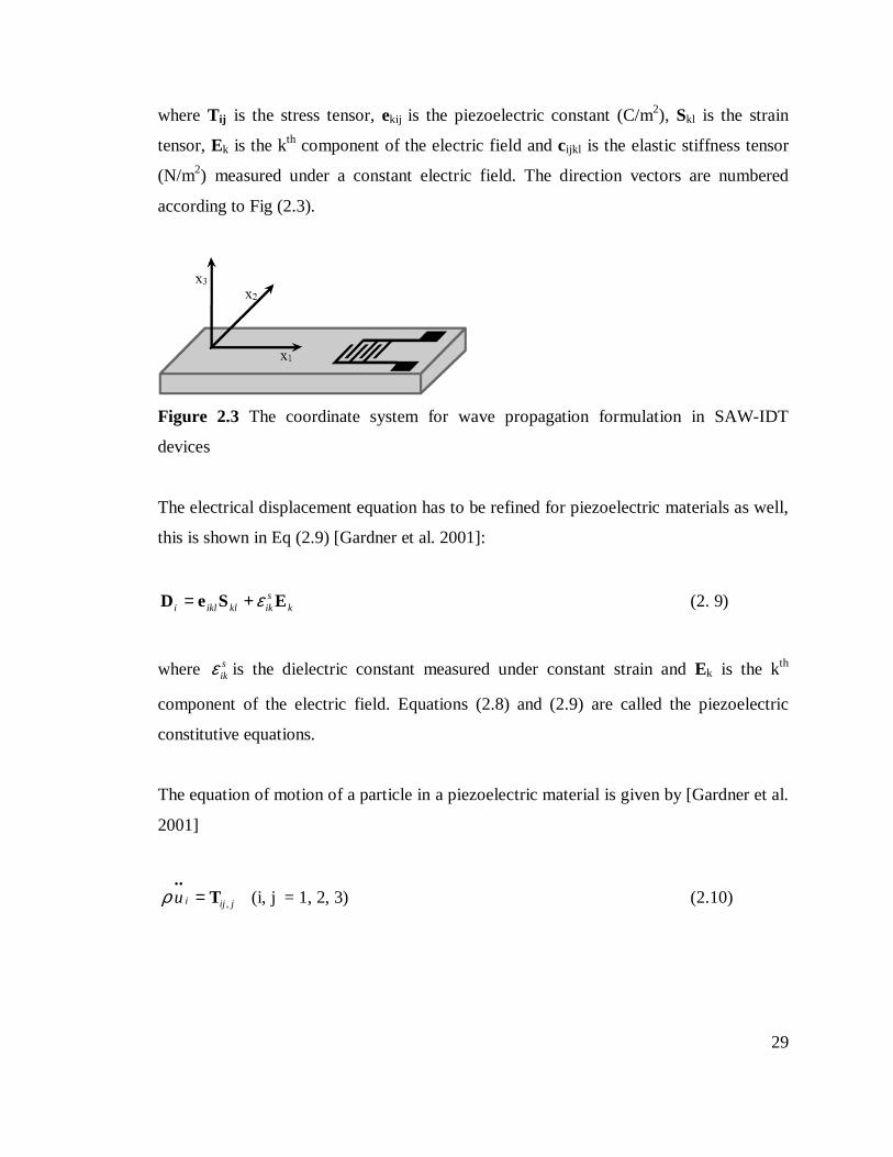
where Tij is the stress tensor, ekij is the piezoelectric constant (C/m2), Skl is the strain
tensor, Ek is the kth component of the electric field and cijkl is the elastic stiffness tensor
(N/m2) measured under a constant electric field. The direction vectors are numbered
according to Fig (2.3).
Figure 2.3 The coordinate system for wave propagation formulation in SAW-IDT
devices
The electrical displacement equation has to be refined for piezoelectric materials as well,
this is shown in Eq (2.9) [Gardner et al. 2001]:
ksikklikli ESeD ε+= (2. 9)
where sikε is the dielectric constant measured under constant strain and Ek is the kth
component of the electric field. Equations (2.8) and (2.9) are called the piezoelectric
constitutive equations.
The equation of motion of a particle in a piezoelectric material is given by [Gardner et al.
2001]
jijiu ,T=••
ρ (i, j = 1, 2, 3) (2.10)

30
where ρ is the mass density, ui is the particle displacement and jij ,T represents j
ij
x∂∂T
, (x
representing one of the principal directions). The strain-mechanical displacement is
defined by [Gardner et al. 2001]:
klijklklijkl ,ucSc = (2.11)
For piezoelectric applications, the wavelength of the elastic waves is much smaller than
the electromagnetic wavelength hence the magnetic effects generated by the electric field
can be neglected and the following relation can be written:
kk ,φ−=E (2.12)
where φ is the electric potential associated with the acoustic wave. If Equations (2.8)
through (2.12) are combined with the assumption that there are no intrinsic charges in the
materials, the following equations that govern the propagation of surface acoustic waves
can be written as:
jkkijjklEijkliu ,, φρ euc +=
•• (2.13)
jkSjkjkljklue ,,0 φε−= (2.14)
The SAW-IDT devices further impose what is known as the traction-free boundary
conditions [Viktorov 1967] of:
03 =iT for x3 =0 (where i = 1, 2, 3) (2.15)

31
2.5.2 Design Considerations for SAW Devices
The first design consideration is to select the appropriate waveform on the SAW
substrate. The general solution of Equations (2.13) and (2.14), where all three-particle
displacement components exist, is called the generalized Rayleigh waves. Depending on
the crystal orientation, symmetry and boundary conditions, other waveforms are
generated. The common waveforms are Rayleigh, S-waves, Love and compressional
waves. A description of these waveforms is given in Table (2.1).
Table 2.1 Typical waveforms and their properties in piezoelectric substrates
Waveform Propagation direction
Particle movement direction
Type Properties
Compressional x1 x1 Bulk Propagates like sound
waves in air.
Rayleigh x1 x3 Surface
Propagates like ripples on water. Common in SAW-IDT applications
Love x1 x2 Surface Poor coupling to gas and/or liquid interfaces. Common in SAW-IDT applications
S-wave x1 x3 Bulk Propagates like a wave on a string
When an AC voltage is applied across an IDT, a stress wave is generated inside the
piezoelectric crystal and propagates in the transverse direction to the IDTs. To create a
constructive interference of these wave patterns, the distance between the IDT fingers
should be exactly equal to the half of the elastic wavelength of the SAW such that:
2Rd
λ= (2.16)

32
where λR is the elastic wavelength of the crystal. If the electrical frequency is the same as
the wave propagation frequency, the energy conversion efficiency at the IDTs is
maximized. Therefore SAW-IDT devices are designed to operate at certain carrier center
frequencies.
One of the design parameters for SAW-IDT devices is the electromechanical coupling
coefficient, k2, which is a measure of the efficiency in converting an applied radio
frequency signal into mechanical energy associated with the surface acoustic wave. At a
given relative bandwidth, it determines the insertion loss of the device. Both the wave
propagation velocity and k2 depend (among other factors) on the material properties of
elasticity, piezoelectricity, dielectric permittivity, and mass density. Different wave types,
propagating in different crystalline directions on different substrate materials, show
different wave velocities and coupling coefficients. Properties of some frequently used
SAW substrate material cuts are given in Table (2.2).
Table 2.2 Properties of the common piezoelectric substrates
Orientation Material
Cut Prop.
v [m/s]
k2 α
[ppm/oC]
ST X 3158 0.1% 0 Quartz 37°rotY 90°rotX 5094 0.1% 0
Y Z 3488 4.1% 94
41°rotY X 4750 15.8% 69 LiNbO3 128°rotY X 3980 5.5% 75
LiTaO3 36°rotY X 4220 6.6% 30

33
CHAPTER 3
PROPOSED PASSIVE WIRELESS TELEMETRY FOR HIGH-FREQUENCY
SENSOR MEASUREMENTS
3.1 Proposed Inductive Coupling Based Continuous Wave Mode Operation
3.1.1 Description of the Methodology
The proposed passive wireless sensing scheme does not utilize the impedance phase (or
amplitude) dip detection method and aims to detect the real-time impedance change of
the external circuit while constantly exciting the sensor with an RF signal closer to its
natural frequency. Since the current on the transceiver circuit is modulated by the
changes in sensor capacitance, it is possible to calculate the capacitance by reading the
impedance of the transceiver circuit. The external circuit impedance can be detected by
using the I-V method for impedance detection at measurement frequencies through
analog I-Q demodulation. The simplified schematic of the setup for the proposed passive
inductive coupling wireless scheme is given in Fig (3.1).
Figure 3.1 Simplified diagram of the proposed telemetry system

34
Using real-time demodulation also has the distinct advantage of being able to apply
model based approaches and creating algorithms to enhance the performance of the
inductive coupling scheme. These algorithms can be used for every system and do not
depend on hardware improvements hence they add flexibility to the telemetry system
design.
3.1.2 Mathematical Model of the System The mathematical model of the system is based on the coil equations of two magnetically
coupled coils. The coil equations are derived from the principle of mutual inductance
between the two coils. When the impedance of the sensor changes, the current in the
secondary coil changes, which in turn changes the primary-coil’s current, as shown in
Equations (3.1) and (3.2).
dt
diMdti
Cdt
diLiRRtV xin
21
1
1111
1)()( −+++= ∫ (3.1)
dt
diMdti
Cdt
diLiR 1
22
2222
1 =++ ∫ (3.2)
This change in the primary current may be seen across a resistor and used to detect the
change in impedance in the secondary circuit. A detailed circuit model of the telemetry
system is shown in Fig (3.2).

35
Figure 3.2 A detailed circuit diagram for the inductive coupling operation
In the setup of Fig (3.2), L1, C1, R1 and L2, C2, R2 are the inductance, capacitance and
resistance of the transceiver (i.e. circuit 1) and sensor circuits (i.e. circuit 2) respectively.
Z21 is the load impedance on the transceiver circuit due to the passive sensor circuit. Vin is
the RF input to the transceiver circuit, Rx is the resistor across which measurements are
made and Vout is the voltage output read across the resistor Rx.
3.2 Straightforward Telemetry Scheme Based on Time Domain System Model
Equations (3.1) and (3.2) give the time-domain based model of the system. If the system
model parameters are known, a straightforward solution of this system of equations can
be performed in order to calculate the sensor capacitance C2. The block diagram of the
solution is given in Fig (3.3).
The solution shown in Fig (3.3) is best suited for designing an analog high frequency
signal processing circuit, though it is also possible to use high frequency sampling (i.e. at
least 10-20 times the bandwidth of the system) to digitize the signals Vx(t) and Vin (t).

36
Figure 3.3 A block diagram of the straightforward solution of the time-domain system of
equations
The straightforward approach requires knowledge of the mutual inductance term M. M,
as defined in Eq (2.1), contains the inductances of the sensor and transceiver coils, which
are known, and the inductive coupling coefficient k. It is possible to model the static
coupling coefficient between two coil antennas. However the coupling coefficient
between two coils with different radii, number of windings and height are actually
described by a formula containing elliptic integrals. This makes evaluation complicated.
Based on a series of expansions, Grover [1946] published a formula replete with look up
tables of some of the necessary terms. In most cases, multiple interpolation steps are
needed to compute several of the terms. This gives rise to errors in the final calculation
and usually, in real systems involving static mutual inductance, M is found
experimentally.
Experimental determination of M might be sufficient for applications where the coupling
between the antennas is constant throughout device operation. This implies that the
relative distance and orientation of the sensor and the transceiver coils have to be kept

37
steady. The problem arises in inductive coupling telemetry where there is movement
between the coil antennas, such as in biomedical monitoring applications. This would
certainly affect the measurement of C2. In biomedical monitoring applications, this
change may be caused by a combination of the movements of the patient or the operator
holding the transceiver. In cases where the sensor is implanted inside the body and
designed to sense a parameter closely related to the movement of body parts, such as in
the case of a wireless IMP sensor application, the frequency of the relative movement
between the antennas and the rate of change in the coupling coefficient are identical. This
makes it harder to filter its effect on the modulation. In lieu of these limitations of the
straightforward strategy, it is necessary to devise a telemetry method that would eliminate
the need to know the mutual coupling term.
3.3 Development of Novel Algorithms for Inductive Coupling
The work by Cho and Asada [2003] is the first investigation on the estimation of sensor-
capacitance by applying a frequency domain approach. The cited work utilizes a
recursive least squares estimator to estimate both the capacitance and mutual inductance.
The highly non-linear characteristics of the system necessitates the employment of a
forgetting factor to suppress the influence of measurement noise and consequently slows
down the estimator and results in the algorithm being unable to track high frequency
changes in sensor-capacitance.
Instead of attacking the non-linear problem by using recursive estimation, the algorithms
developed in this thesis, introduce an algebraic approach to eliminate the mutual
inductance term from the system of equations, resulting in direct calculation of the
measured capacitance change.

38
3.3.1 Frequency Domain System Model
Apart from the time-domain equations that give the system dynamics as in Equations
(3.1) and (3.2), a frequency domain model can also be created [Cho and Asada 2003]. A
frequency domain transfer function between the voltages Vout (jω) measured across the
resistor Rx in Fig. (3.2) and the input voltage Vin (jω) can be written as:
)1
()
1(
)(
)(
2222
22
12101
CLjR
M
CLjRRR
R
jV
jV
x
x
in
out
ωω
ωω
ωωω
−++−+++
= (3.3)
where R0 (not shown in Fig 3.2) is the series internal resistance of the power supply.
3.3.2 Simulations
a. Sensitivity analysis
The performance of the resonant frequency detection methods can be quantified in terms
of their sensitivity defined by the change in resonant frequency per capacitance change
(MHz/pF). In the proposed method, on the other hand, the interrogation frequency is kept
constant and the goal is to determine the frequency at which the effect of the sensor
capacitance change on the voltage output is maximized. Hence the sensitivity can be
defined as:
2
)(
)(
C
jV
jV
S in
out
∂
∂=
ωω
(3.4)
The resulting term in Eq (3.4) is very complex and therefore will not be repeated here. Eq
(3.3) defines a complex non-linear system with several variables that can be tuned during

39
the design of the telemetry system. The analytical determination of how these variables
affect sensitivity is challenging and results in very complex terms that lose their
practicality. For instance if the effect of the RF operation frequency (ω) on sensitivity is
formulated, the resulting solution amounts to finding the roots of a 10th degree
polynomial in variable ω. On the other hand, the success of the telemetry system depends
on understanding how design parameters affect sensitivity and therefore the effects of
important design parameters on system performance have to be addressed by performing
a series of simulations.
b. Effect of carrier RF frequency on sensitivity
Commonly in the literature, a frequency sweep is performed and the resonant frequency
of the sensor is determined by checking the dip in the sensor current i2, which is shown in
Fig (2.2). Here a very similar simulation will initially be performed to determine the
relationship between the RF signal frequency and the magnitude of the transfer
function)(
)(
ωω
jV
jV
in
out . The result of this simulation is given in Fig (3.4.a).
The effect of RF telemetry frequency on the sensitivity function given in Eq (3.4) is
plotted by calculating the analytical sensitivity function and varying the telemetry
frequency. The main goal of this simulation is to determine the frequency at which, for a
given capacitance change ∆C2, the change in the output voltage is maximized. The result
of this simulation is given in Fig (3.4.b). It has to be noted that the curve in Fig (3.4.b)
shows how sensitivity varies with frequency for a specific C2. However the sensitivity is
also a function of capacitance and hence for finite changes in sensor capacitance, the
curve no longer accurately represents the sensitivity with varying telemetry frequency.
In order to determine the effect of telemetry frequency on sensitivity for finite changes in
sensor capacitance C2, another simulation was performed. This time, the sensor
capacitance C2 was varied in a sinusoidal manner from its nominal value 02C and the
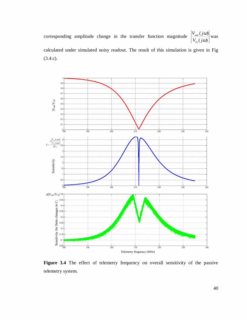
40
corresponding amplitude change in the transfer function magnitude )(
)(
ωω
jV
jV
in
out was
calculated under simulated noisy readout. The result of this simulation is given in Fig
(3.4.c).
Figure 3.4 The effect of telemetry frequency on overall sensitivity of the passive
telemetry system.

41
The results clearly show that the resonant frequency of the sensor is actually the point
where the sensitivity to the sensor capacitance change is at a minimum. Hence operation
at the resonant frequency srω should be avoided. The maximum sensitivity appears at a
frequency close to srω . However, in view of the fact that this is a non-linear system, the
sensitivity analysis shown here should be repeated to find the frequency where the
sensitivity is maximum for that specific configuration.
c. Effect of the sensor resistance on system performance
The sensor resistance R2 has been found to have a profound effect on the overall
performance of the system. Minute changes in R2 affect the sensitivity of the telemetry
system greatly. Ideally, in the case that the sensor resistance is zero, all of the energy that
is imposed on the sensor by the transceiver would be utilized in the sensor reactance.
Instead this energy is lost on the resistor which effectively decreases the quality factor of
the sensor. Simulation results given in Fig (3.5) depict the importance of having a small
series resistance on the sensor circuit.

42
Figure 3.5 The effect of the sensor resistance R2 on wireless telemetry
d. Effect of coil inductances on system performance
In order to simulate the effect of coil antenna inductances on system performance, the
L1/L2 ratio was varied while the tuning capacitance C1 was changed, to keep the resonant
frequencies of the two circuits constant. C2 cannot be changed since it is defined by the
capacitance of the sensor. For each combination of the C1, L1 pair, the simulation shown
in Fig (3.4.c) has been repeated and the maximum change in the transfer function
amplitude (i.e. maximum achievable sensitivity) and its corresponding frequency have
been calculated. Simulation results, given in Fig (3.6), show the variance of these two
components with the changing L1/L2 ratio. In Fig (3.6), max
/ inout VV∆ refers to the

43
maximum change in the transfer function amplitude for a given amount of change in
capacitance and ∆maxf is the frequency at which this change occurs.
Figure 3.6 The effect of antenna coil inductances on system response
The simulation result shown in Fig (3.5) suggests that the ratio (L1/L2) should be kept as
low as practically possible. In a real application, the effect of the sizes of the coil
antennas on the coupling coefficient has to be considered. The coil antenna inductances
are a function of their size as well as other geometric factors such as coil spacing and
thickness etc. The independence of choosing these factors freely may be limited by the
application. Parasitic effects, such as the series resistance of the coil antenna that might
be associated with a higher inductance on the sensor circuit, should also be considered as
their adverse effect on wireless system performance was shown in Fig (3.5).

44
3.3.3 Frequency-Domain Based Cascaded Filter
In order to overcome problems associated with the straightforward estimation of sensor
capacitance, a novel cascaded filter was designed. The filter estimates the inverse
capacitance C2 and mutual inductance M successively, and does not require prior
knowledge of the latter to calculate capacitive measurements. The method is based on a
fast algebraic approach that does not put any theoretical limits on the bandwidth of the
sensor measurements.
In order to develop the measurement equations, the inverse of the frequency domain
transfer function between ( )outV jω and ( )inV jω , given in Eq (3.3), is taken as:
)1
(
)1
(
1)(
)(
2222
221
2101
CLRjRR
M
R
CLj
R
RR
jV
jV
xxxxout
in
ωω
ωωω
ωω
−++
−+
++= (3.5)
The real and imaginary parts of the transfer function given in Eq (3.5) are denoted as
))(
)(Re(1 ω
ωjV
jVz
in
out= and ))(
)(Im(2 ω
ωjV
jVz
in
out= , which can be measured directly from the I and
Q readings through an I-Q demodulator attached across the measurement resistor Rx. The
two unknown variables are then defined as 2
1
1
Cx = and 2
2 Mx = . Then, by expanding Eq
(3.5), the expressions for the two measurements1z and 2z can be found, as they relate to
the unknowns x1 and x2 in the following manner:

45
−+
−−
−
−++
++
=
2
222
2222
2
2222
2
121
2
222
2222
2
222
01
2
1
)1
(
)1
()1
(
)1
(1
CLRRR
CLRx
R
CL
CLRRR
RRx
R
RR
z
z
xx
x
x
xx
x
x
ωω
ωω
ωω
ωω
ω
(3.6)
This is a non-linear algebraic problem involving two measurements1z , 2z , and two
unknowns, 1x , 2x . In order to find the values of1x and 2x , a closed form solution of Eq
(3.6) is required.
If two new parameters are defined as:
xR
RRzy 01
11 1+
−−= (3.7)
and
xR
CL
zy
)1
(1
21
22
ωω −
−= (3.8)
Eq (3.6) can be rewritten as:
−+
−−
−+
=
2
222
2222
2
2222
2
2
222
2222
2
222
2
1
)1
(
)1
(
)1
(
CLRRR
CLRx
CLRRR
RRx
y
y
xx
x
xx
x
ωω
ωω
ωω
ω
(3.9)

46
If y1 is divided by y2, the fairly complex denominator and the term xRx22ω in the
numerators are cancelled out as seen in Eq (3.10).
222
2
2222
2
2
222
2222
2
2
222
2222
2
222
2
1
1)
1(
)1
(
)1
(C
L
R
CLRx
CLRRR
CLRRR
RRx
y
y
x
xx
xx
x
ωωω
ωω
ωω
ω
−
−=
−−
−+⋅
−+=
(3.10)
Hence the unknown mutual coupling term included in the unknown x2 has been
eliminated from the system of equations. Consequently the capacitive measurement C2
can be calculated by first calculating the unknown x1 from equations (3.7), (3.8) and
(3.10) as:
−−
++−+=
)1
(
)(
1212
01122
21
CLjRz
RRRRzRLx
x
xx
ωω
ω (3.11)
The unknown1x , hence the capacitance measurement C2, is calculated linearly by
dividing the two manipulated measurements. If knowledge of the mutual coupling is
desired, the value of 1x is then substituted in Eq (3.6) to obtain2x , hence the term,
cascaded filter. It should be noted that the value of 2x is not critical for passive wireless
sensing since the value of the mutual inductance provides no information about sensor
measurements.
The simple cascaded filter would provide accurate estimates of the state 11 /1 Cx =
imposing no constraint on the maximum achievable frequency. The proposed algorithm
requires the demodulation of the output voltage Vout which can be accomplished by a

47
variety of methods including I-Q demodulation. The algebraic solution, which directly
calculates the sensor capacitance from the measurements, is fast and does not need the
prior knowledge of the coupling coefficient. This makes the method ideal in sensing high
frequency changes in sensor capacitance hence better suitable for high-frequency sensing
with inductively-coupled batteryless wireless sensors.
3.3.4 Modified Circuit Model and the Modified Cascaded Filter
In real high frequency circuits, the assumption of purely resistive or purely reactive
elements is not accurate. Even in cases where high frequency-stable elements are used,
the way these components are attached to the circuit board changes their equivalent
response. For instance there are several models for different mounting conditions of
resistors on the circuit board, each introducing a different network model. A small ball of
solder in fact might add an inductance value as much as 10 nH and makes the assumption
of pure resistive element invalid. Hence for an accurate system model, a modified version
of the cascaded filter has to be derived.
If the parasitic reactance of the resistor Rx is defined as jZx, then Eq (3.3) can be rewritten
as:
)1
()
1(
)(
)(
2222
22
1211
CLjR
M
CLjRjZR
jZR
jV
jV
xx
xx
in
out
ωω
ωω
ωωω
−++−+++
+= (3.12)
Following the same routine to derive Eq (3.5), and defining the unknowns z1 and z2 in a
similar fashion to Eq (3.6), the modified version of Eq (3.6) can be written as:

48
+−
+
−−
++
+
−++
=
22
22
22
1
121
22
22
22
1211
mod2
mod1
)1
(
)1
(
1
BA
Bx
ZR
ZRC
LR
BA
Ax
ZR
CLZRR
z
z
xx
xx
xx
xx
ωωω
ωωω
(3.13)
where
)( 21
22 ωω x
LZRRA xx −−= (3.14)
and
xx ZRx
LRB 221
2 )( +−=ω
ω (3.15)
The modified version of the variables y1 and y2 in Eq (3.9) can be denoted as y1mod and
y2mod, and these parameters can be defined as:
+−
+=
+
−−−
+
−+−−
=
222
2
222
2
22
11
21
mod2
221
211
mod1
mod2
1mod
)1
(
)1
(
1
BA
BxBA
Ax
ZR
ZRC
LR
z
ZR
CLZRR
z
y
y
xx
xx
xx
xx
ω
ω
ωω
ωω
(3.16)
Taking the ratio of ymod1 and ymod2 yields:
xx
xx
ZRx
LR
RRx
LZ
B
A
y
yY
221
2
221
2
2mod
1mod
)(
)(
+−
−−=−==
ωω
ωω
(3.17)
Hence the unknown x1 can be found by using the following equation:

49
xx
xxxx
ZYR
RRLZYZRYLRx
−+−+
= 22
2222
1
ωωωω (3.18)
Using the modified version of the cascaded filter is necessary in all real applications for
accurate detection of the capacitance change.
3.4 Proposed SAW-IDT Based Operation with Pulse-Echo Type Modulation:
3.4.1 The Mathematical Model
A mathematical model of the SAW device based on the coupling of modes (COM) theory
is employed to derive the relation between the change in the reflected signal of the SAW
sensor and its load impedance. The P-matrix formulation [Tobolka 1979] is a
representation of the COM theory relations between the acoustic and electrical waves in
the SAW device. The P-matrix parameter to describe the reflectivity of the impedance-
loaded IDT is given in Eq (3.19) [Reindl and Ruile 1993, Ruile 1994].
load
sc
ZP
PPP
12
33
213
1111
++= (3.19)
where iiP represents an element of the P-matrix. 11P is the complex acoustic reflectivity
of the load IDT, scP11 is the reflectivity of the load IDT when short-circuited. It is
approximated as zero for split-finger IDTs similar to those used in this work. 13P and 33P
are the electro-acoustic coupling coefficient and electrical admittance of the IDT
respectively. 13P , 33P are constant for a given SAW device and depend on the substrate
material and IDT geometries [Steindl et al. 2000]. loadZ is the complex impedance the
load IDT sees and is given in Eq (3.16) :

50
load
jZ R jL
Cω
ω= + − (3.20)
where R, L and C represent the parameters of the equivalent load circuit; ω is the center
frequency of the SAW-IDT sensor. The non-linear relation described in Eq (3.19) results
in non-unique solutions for measured capacitance for certain values of series inductance
(L) as described by Steindl et al. [1999]. In order to select a proper series inductance (to
have a unique capacitance value for a given reflectivity), the values of P13 and P33 and the
impedance of the wire bonding should be determined experimentally.
3.4.2 SAW-IDT Integration for High Frequency Acoustic Sensors
A model that can be used for SAW-IDT high frequency capacitive membrane based
sensor integration is proposed. However it should be noted that the presented method is
not limited to use with these types of sensors and any kind of impedance varying sensor
can be integrated successfully for high frequency operation.
In the case of a capacitive membrane based high frequency MEMS sensor, such as a
microphone, the membrane responds to sound pressure by a change in its capacitance as
shown in Eq (3.20). For small variations in the pressure, if the complex relationship
between the sound pressure and the magnitude P11 through equations (3.19) and (3.20) is
approximated as a linear relationship as follows:
11 .P K P= (3.21)
where K is a constant of proportionality and P is the pressure acting on the diaphragm
which is given by:

51
= +o soundP P P (3.22)
where oP is the ambient pressure acting on the diaphragm and soundP is the fluctuating
sound pressure. Since the amplitude of the acoustic reflectivity varies linearly with
acoustic pressure, the magnitude of 11P can be written as in Eq (3.23)
11 11 11varconstP P P= + (3.23)
where 11 constP is the constant amplitude of acoustic reflectivity in the absence of any
impedance change on the load IDT, var11P is the variation in the amplitude of the acoustic
reflectivity with the changing impedance/pressure. From Equations (3.22) and (3.23)
11 constP can be written as:
11 11 var( )const o soundP P K P P+ = + (3.24)
Hence the following equations can be written:
11 var( )sound
d dP K P
dt dt= (3.25)
or
11 var
1( )sound
d dP P
dt K dt= (3.26)
Equation (3.26) shows that the variation in the acoustic reflectivity is proportional to the
variation in sound pressure. In other words, the varying component of the measured
acoustic reflectivity represents a scaled change in the sound pressure level. Therefore, the
sound signal can be regenerated by measuring the change in the amplitude of the acoustic
reflectivity 11P without any need for calibration.

52
In conventional microphones, the changes in sound pressure levels induce a small voltage
change, which is then amplified to retrieve the original signal. While the initial or
nominal value of the physical quantity is important only for maximizing the sensitivity of
the device, it is irrelevant for detecting the relative change in sound pressure levels at
different frequencies. In the case of the SAW sensor, it is the acoustic reflectivity that
varies linearly with sound pressure. Thus, by measuring the change in the acoustic
reflectivity, it is possible to retrieve the sound detected by the MEMS microphone which
essentially works as a variable capacitor.
The linearity of the relationship between the reflectivity of the SAW sensor and the
capacitance change is given in Fig (3.7.a) which is obtained experimentally by using a
varactor as the changing capacitance [Sivaramakrishnan 2006]. Figure (3.7.b) shows the
simulated relationship between the acoustic pressure and the corresponding capacitance
change for a silicon condenser microphone with an 800 µm diameter circular Si3N4
membrane and 400 µm diameter electrodes (both the membrane thickness and the
capacitive gap are 0.8 µm).
Figure 3.7 a-) Experimental results showing acoustic reflectivity with changing
capacitance b-) simulated relationship between the acoustic pressure and the
corresponding capacitance
53
CHAPTER 4
MEMS DEVICE DESIGN AND MICROFABRICATION
Two types of sensors have been designed and fabricated to be tested with the passive
wireless telemetry system in order to be able to create a miniature sensing package for
high frequency measurements. A new surface micromachining based microfabrication
strategy has been developed to create capacitive membrane based MEMS sensors for a
broad range of applications including high frequency sensors such as microphones or
capacitive micromachined ultrasound transducers (cMUTs). SAW-IDT sensors have also
been designed and fabricated to be tested for their performance in measuring high
frequency capacitance change.
4.1 Basic Design Considerations for the Capacitive MEMS Sensor Design
Capacitive sensing has been proven to be the one of the most effective sensing strategy
for MEMS sensors for their superior sensitivity, signal to noise ratio and long term
stability [Ning et al. 1996]. Sensors operating at higher frequencies such as silicon
microphones and cMUTs have also been proven to be successful in the literature
although piezoelectric microphone designs are also common [Ko et al. 2003]. Some
capacitive designs require an external DC bias voltage [Mullenborn et al. 2001] whereas
some have electret layers deposited on one of the electrodes to provide a constant charge
between capacitor plates [Amjadi 2000, Kressmann et al. 2002]. In the capacitive MEMS
(and conventional condenser sensors) high frequency sensors, the DC-bias or the charged
electret layer are necessary to supply an electric field strength that is considered to be
constant across the capacitive gap as the diaphragm vibrates under changing acoustic

54
pressure. The capacitance change creates a small-signal AC voltage across the electrodes,
which is then amplified to obtain the sensor readings.
4.1.1 Selection of the Fabrication Type: Bulk or Surface Micromachining
The most important parameters that affect the response of a MEMS capacitive sensor are
the structural design of the membrane and the height of the capacitive gap. Important
response characteristics such as the dynamic range and sensitivity of the sensor are
defined by these two parameters.
The membrane of a MEMS capacitive sensor can be fabricated either from single crystal
silicon via bulk-micromachining or from a variety of materials deposited as thin-films by
using surface micromachining. Bulk micromachining results in stress-free membranes
[Kovacs and Stoffel, 1994] but usually incorporates the tedious wafer-bonding process.
In this common fabrication theme, the back-plate and the membrane are fabricated on
separate wafers which are then joined by anodic or direct silicon bonding to form the
sensor [Rudolf and Bergqvist 1991]. There are two main disadvantages of this scheme.
One is related to the success rate of wafer bonding technologies. Despite the high
strengths of the bond they form, both direct silicon bonding and anodic bonding require
the two wafer surfaces to be extremely flat. Any small impurity on the wafer surfaces will
create large gaps in the bond resulting in lower yields or a non-functional bond
[Mullenborn et al. 2001].
Another problem lays in the way bulk micromachining works. In order to get high
sensitivity from a miniature capacitive sensor, the membrane has to be very thin, usually
between 0.5 – 5 µm, and the capacitive gap has to be very small. The aim in bulk
micromachining is to etch the silicon substrate (a standard silicon wafer is 500 um thick)
down to the membrane thickness. Hence, either an etch stop layer is needed or a precisely
controlled timed-etch should be performed in order to thin-down the wafer to the desired
membrane thickness. The etch stop layer adds further complexity and cost to the

55
fabrication process in the form of either ion-implantation for electrochemical etch stop
[Miao et al. 2002], deposition of an additional layer of etch mask or starting the
fabrication with an SOI wafer with buried etch-stop layer. In most cases, timed etch is
extremely impractical and decreases the yield as a result of the varying across wafer etch
rate both in anisotropic wet KOH etching and dry plasma DRIE etching. The challenge
can be eased slightly if thin wafers (i.e. wafers thinner than 200 um) are used however
these wafers impose handling challenges and are costlier to produce.
Surface micromachining eliminates most of the problems described in the preceding
paragraphs. Since the membrane thickness is controlled precisely by monitoring the thin-
film deposition rate and time, there is no need for complex routines like etch-stop layers
or timed-etches. The capacitive gap is formed by deposition, patterning and removal of a
sacrificial layer and can be controlled precisely as well. The only disadvantages of the
surface micromachining are the intrinsic stress in the membranes associated with the
high-temperature deposition processes and the stiction of the membrane after the
sacrificial layer etch and release. Although it is possible to solve the stiction problem by
facilitating the release in a critical point dryer, the problem of stress in the membranes
remains a challenge.
4.2 Challenges of Fabrication
The requirements of the proposed sensing strategy forces physical restrictions on the
sensor to be used in conjunction with the telemetry system. These restrictions translate
into challenges in the microfabrication scheme to create the sensors and can be listed as
follows:
a. Electrodes should be metal: The overall resistance on the passive sensor circuit
has a profound effect on the overall sensitivity of the inductive coupling telemetry
system and should be minimized. The importance of minimizing resistance is
shown in the simulation results (Fig 3.5). Commonly described in the literature,

56
one way to create the electrodes, usually the bottom electrode, of capacitive
sensors is to use the substrate which is heavily doped to decrease resistivity [Jin et
al., 1999]. This method has its advantages since there is no additional material
added on to the substrate creating steps to cover in the proceeding deposition
steps, and the electrode is made of silicon which usually has excellent etch
selectivity over most common sacrificial layer materials. It is also possible to
construct the membrane of the sensor along with the electrode by using bulk
micromachining of single crystal silicon. However even highly doped silicon has
significantly higher resistivity than the common metals used for metallization
(e.g. minimum resistivity of highly doped silicon: 1.10-5 Ωm, resistivity of
aluminum: 2.82.10-8 Ωm). Therefore using doped silicon will introduce
unnecessary series resistance on the passive wireless circuit. As a result of these
factors that might affect sensor performance, both electrodes of the capacitive
sensor have to be metalized.
b. Capacitive gap should be minimized: The sensitivity of a sensor is always
important; however if the sensor is going to be part of a passive wireless circuit,
then maximizing sensitivity becomes one of the priorities, since the amount of
change in capacitance directly effects not only the overall sensitivity of the device
but also the telemetry distance. In capacitive sensors, when parallel plate
assumption is made, the electrical sensitivity can be defined as:
20
0 )(
d
A
dd
A
d
CS r
r
e
εεεε
−=∂
∂=
∂∂= (4.1)
where εr and ε0 are respectively the relative and vacuum permittivity, A is the area
of the electrodes and d is the gap between the electrodes. It is clear from Eq (4.1)
that the capacitive gap is the most important parameter in defining electrical
sensitivity and should be minimized. Surface micromachining gives very precise
control over the height of the capacitive gap.

57
c. Low temperature compatible fabrication process: As previously described in
Chapter 1, one of the advantages of using a MEMS sensor in passive wireless
telemetry is the compatibility of MEMS processing with pre or post-CMOS
fabrication. This enables the whole sensor unit, including the necessary passive or
active circuit elements as well as the antenna coils, to be fabricated on chip
without the need for further assembly steps [Cunningham and Bernstein, 1997]. It
is important to note that this project does not aim to develop one such system;
nevertheless developing a CMOS compatible process has been one of the
priorities for future applications demanding wafer level integration. The
fabrication scheme has been designed to conserve the post-CMOS compatibility
and hence only low temperature processes (i.e. <340°C) have been utilized. With
proper isolation and protection of the CMOS components, the fabrication strategy
can be performed post-CMOS, without affecting transistor characteristics.
4.3 Selection of the Membrane Material
Silicon nitride (SiNx) has proven to be an excellent material to construct structural thin
film membranes and has been widely used to create membranes for MEMS sensors.
There are mainly two ways of chemical deposition of SiNx; low pressure chemical vapor
deposition (LPCVD) and plasma enhanced chemical vapor deposition (PECVD).
LPCVD nitride films which are more commonly used in microfabrication are higher
quality films in terms of providing better insulation, lower defect density and higher
density. However as a result of the high temperatures associated with the process, the
resulting films suffer from high tensile stresses. The stoichiometric or standard LPCVD
nitride is chemically balanced with an exact stoichiometry of Si3N4 and is an excellent
insulator. However it suffers from high tensile film stresses (over 1000 MPa) and for
most of the sensor applications it can not be used as membrane material. Another form of
nitride, low stress nitride can also be deposited in LPCVD chambers to create a silicon

58
rich nitride (SiNx), which has film stresses around 300 MPa or lower. This enables the
use of low-stress nitride films to be successfully used in thin-film membranes [Gogoi et
al. 2001]. Furthermore, the high temperatures associated with the LPCVD process also
limit the presence of most metals or other materials that are high-temperature
incompatible on the wafer, hence significantly restraining the process flow of a MEMS
fabrication sequence. Most microfabrication facilities also strictly limit the materials that
can go inside the deposition furnace for LPCVD for the risk of contamination. Even if the
fabrication sequence is planned so that the membrane deposition is made before
metallization, these membranes suffer from very high stresses and other methods like
designing corrugated membranes or successive annealing steps have to be introduced
before the membranes are released [Bourouina et al. 1995].
PECVD films on the other hand are deposited under lower temperatures ranging from
100°C up to 350°C and as a result suffer less from the negative effects of intrinsic film
stress than LPCVD films. Furthermore, PECVD chambers are usually used for a range of
chemical processes with or without plasma and there are no strict restrictions on the kind
of materials that are permitted on the wafer. However, they have larger defect densities
and are considered to have inferior quality and therefore examples of LPCVD membranes
are more commonly found in the literature. There has been recent work that shows
PECVD can be used successfully for mechanical membranes. Dell et al. [2002] report
successful use of PECVD nitride as membrane material for variable MEMS-based
inductors. Winchester and Dell [2001] investigate stresses in the PECVD nitride
membranes to be used in Fabry-Perot interferometers and Noble et al. [2001] report the
use of PECVD SiNx as membrane material to fabricate cMUTs.
The flexibility to tailor the fabrication process sequence, the lower intrinsic stresses in the
resulting film and the relative inconsequentiality of electrical isolation needed for the
proposed acoustic sensors are advantages of PECVD nitride films for the purposes of this
project. As a result, PECVD SiNx has been selected as the membrane material for the
capacitive sensors.

59
4.4 Selection of the Sacrificial Layer and the Electrode Metal
In surface micromachining the membrane and the sacrificial layer have to be determined
simultaneously to obtain a significant etch selectivity during the removal of the sacrificial
layer. In order to determine the best candidate for the sacrificial layer, a series of
experiments were first performed to determine the best membrane-sacrificial layer pair.
4.4.1 Investigation of PECVD SiO2 as Sacrificial Layer
The first material that was tested was PECVD SiO2. It has been used as a sacrificial layer
in conjunction with SiNx in order to successfully create membranes, mostly smaller ones
like those of cMUTs [Soh et al. 1996]. Dry vapor etching of SiO2 in HF would give
stiction free release of the membranes however HF vapor has a destructive effect on SiNx
which changes its morphology and consistency, rendering it useless as a structural layer
[Vereecke et. al., 2000]. Plasma etching techniques are not an option either because of the
significantly higher etch rates of SiNx than SiO2 in fluorine and chlorine based plasma.
The only alternative is the use of wet-etching for the removal of SiO2.
The etch rates of several forms of silicon oxides and silicon nitrides have been
investigated in a study by Witvrouw et al. [2000]. However no work has been done to
characterize PECVD oxide etching to date. BHF:glycerol solution has been reported to be
increase the etch selectivity of oxides over nitrides [Witvrouw et al., 2000] and therefore
was selected for this investigation.
The experiments showed that regardless of the etching solution, it is not possible to
release membranes with a diameter greater than 40 µm using SiO2 as the sacrificial layer.
The etch rate of PECVD nitride actually increases around the etch holes where the
etchants can react with the bottom surface of the membrane as well as the top surface,
further decreasing the membrane thickness around these regions. Hence it is concluded
that although SiO2 – PECVD nitride pair is viable for fabrication of smaller membranes,

60
such as membranes for cMUTs, for the fabrication process sought, which aims to develop
a compatible fabrication scheme for bigger membranes as well, it is not viable.
4.4.2 Investigation of Aluminum Metallization with Chromium Sacrificial Layer
The second choice for the sacrificial layer material was Chromium which was used
successfully in other studies to release nitride membranes with aluminum electrodes as
reported in [Caronti et al., 2006]. In order to investigate the performance of this
combination, initially a simple test was performed to determine the etch rate of PECVD
nitride in chromium wet etchant. The commercial chromium etching solution CR-12S
from Cyantek was used as the etchant. Excellent etch selectivity over PECVD nitride was
achieved with non-measurable etch rates of SiNx even after leaving the specimen for 48
hours in the etching solution.
Aluminum was selected as the electrode material for its excellent resistivity and low-cost
when compared to other low resistivity metals such as gold. Aluminum has finite etch
rates inside the CR-12S chromium etching solution and if not protected during the wet
etching process, the top and bottom layer aluminum metallization can be attacked by the
etching solution. The etch rate of Al in CR-12S was found to be 200 A°/hr. In order to
protect the underlying aluminum from being attacked by the etchant solution, a 2000 A°
PECVD SiNx was deposited between the aluminum bottom metal layer and the chromium
sacrificial layer. This method was successfully used in the literature to release smaller
membranes for cMUTs [Caronti et al., 2006] and was indeed successful in releasing
membranes smaller than 30 µm. However for larger membranes, in the time it takes for
the chromium sacrificial layer to be completely removed, the underlying aluminum was
also attacked as a result of the chromium etcher penetrating through the protective 2000
A° nitride layer. This was believed to be as a result of the pinholes that appear in PECVD
deposited thin films as reported previously in the literature [Allaert and Calster 1985].
The density of the pinholes are known to decrease with increasing process temperature,
61
however they appear even in the presented case where the highest possible temperature
(i.e. 340 °C) was utilized.
In order to test the minimum PECVD SiNx film thickness which would protect the
underlying aluminum layer, a test was performed. Aluminum was deposited on a blank
silicon wafer followed by a 9600 A° PECVD SiNx deposition. The SiNx layer was then
etched in 1200 A° steps down to 1200 A° to create different layer thicknesses. In order to
guarantee the highest quality nitride, the deposition was made in five steps in between
which the chamber was vented and the wafers were cooled down, nitrogen was blown
and wafer was rotated. The wafer was then placed in chromium etching solution CR-12S.
The pinholes were clearly visible as the underlying aluminum layer was attacked by the
etching solution. The defect density was decreasing with increasing nitride thickness and
it is clear that a thick SiNx film such as 6000 A°, despite having pinholes and a resulting
decrease in final yield, could be used as a protective layer for aluminum. However it is
very impractical to deposit such thick films only to protect the electrodes. Films as thick
as 6000 A° will also have an adverse effect on device sensitivity.
It is clear from these results that using PECVD nitride and aluminum-chromium
combination does not work for sacrificial layer etching for membranes larger than 30 µm.
Furthermore, the need for a thick protective nitride layer between the chromium
sacrificial layer and the bottom metallization unnecessarily increases the capacitive gap,
adversely affecting the nominal capacitance and the electrical sensitivity of the capacitive
sensor. Hence the use of an aluminum-chromium combination as the electrode metal and
the sacrificial layer is not viable.
4.4.3 Aluminum Sacrificial Layer and Cr-Au Metallization
Gold is usually not employed in microfabrication for purely electrical applications such
as electrodes and contact pads unless it is critical for device performance. This is because
of the high cost associated with gold deposition and the adhesion problems that gold

62
suffers from, which in turn necessitate a thin adhesion layer deposition usually in the
form of chromium or titanium. Therefore gold was not one of the first candidates for the
proposed microfabrication process. However as the results of the experiments in the
preceding sections suggested, a compatible metallization-sacrificial layer pair which has
an excellent etch selectivity is needed. The electrode metal should also have low
resistivity as explained in the preceding section. Chromium-gold metallization satisfies
both of these requirements. In fact, gold has excellent resistivity which is 13% less than
aluminum (2.44.10-8 Ωm for Au versus 2.82.10-8 Ωm for Al). Therefore these
characteristics of Cr-Au metallization justify the additional cost they impose on the
fabrication process.
Unlike the finite etch rates of Al in chromium etching solution, the conventional
aluminum etching solution has excellent etch selectivity of Al over Cr and Au. This
renders the protective PECVD SiNx layer that was necessary to protect the top and
bottom metallization layers in the preceding cases superfluous. This increases the
capacitance of the sensor and is beneficial for device sensitivity. Therefore using
aluminum as the sacrificial layer and Cr-Au bilayer as the metallization layer provides
excellent remedies for the additional cost of Au deposition.
4.5 First Batch of MEMS Acoustic Sensors
4.5.1 Design of Membrane Geometry
The first generation of the acoustic sensors were designed to have two different
geometric shapes; hexagonal and rectangular. Hexagonal membranes have been used in
the literature in place of circular membranes successfully, especially for cMUT arrays.
The reason behind their selection versus a circular membrane was their relatively similar
performance in terms of sensitivity and resonant characteristics to a similar sized circular
membrane. Circular membranes add additional cost in terms of increasing the number of

63
flashes during mask fabrication. Therefore hexagonal membranes were chosen instead of
circular membranes.
There were two design considerations for the membranes. One was the effect of static
loading that would be present on the membrane in terms of intrinsic stresses. This effect
was investigated to plan the location of etch holes on the membrane. The other
consideration was the dynamic response of the membranes under acoustic load in terms
of the natural frequency of the membranes. In order to determine the static response of
the membranes, finite element analysis was performed by using ANSYS and the results
are shown in Fig (4.1)
Figure 4.1 Membrane design for the first batch of sensors a-) ANSYS model of the
membrane and b-) portion of the mask design showing the membranes
Careful investigation of Fig (4.1.a) shows the stress concentration points on a hexagonal
membrane under static loading. This result is used to determine the best locations to place
the etch holes on the membranes and the corresponding mask design showing the
placement of the etch holes is given in Fig (4.1.b). Etch holes are placed closer to the
corners of the hexagonal membrane where the stress levels are relatively lower, in order
to minimize the chances of inducing crack propagation as a result of the intrinsic stresses
or other static forces that might act on the membrane during the release, such as capillary
action.

64
The dynamic properties were investigated through analytical approximation of the
primary mode of vibration. The natural frequency of a circular plate with clamped edges
is given by:
h
D
R ρω
21
21.10= (4.1)
where ω1 is the first natural frequency of the membrane (in Hz),)1(12 2
3
υ−= Eh
D is the
flexural rigidity, h is the thickness of the membrane, E=160 GPa is the Young’s modulus,
ρ = 2330 kg/m3 is the density and υ = 0.22 – 0.25 is the Poisson’s ratio for silicon nitride.
It is essential to note that the material properties of silicon nitride thin films vary greatly
depending on the deposition process and cannot be modeled accurately during the design
stage. Equation (4.1) however is believed to give a reasonable estimate of the resonant
frequencies of the membranes and the frequency response of similar membranes have
been investigated are well-known in the literature. The membranes ranging from 30 µm
to 2 mm have resonant frequencies between 20 kHz to 13 MHz as calculated by using Eq
(4.1).
4.5.2 Mask Design for the First Batch of Sensors
The proposed fabrication process uses a four-mask surface micromachining sequence.
Masks are designed by using the commercial integrated circuit layout tool ICEDTM by IC
Editors Inc. A brief description of these masks is given in Table (4.1).

65
Table 4.1 Description of the photolithography masks for the microfabrication process
Mask Layer Layer Name Description
1 Bottom Metal Mask for the bottom Cr/Au metallization layer
2 Sacrificial Layer Mask for patterning the Al sacrificial layer
3 Top Metal Mask for the top Cr/Au metallization layer
4 Etch Holes Mask for patterning etch holes on the membrane
One challenge arose during the fabrication of the lithography masks for the first batch of
sensors. The pattern generator which is used for making the lithography masks uses a set
of two L-shaped blades to create an aperture that constitutes a variable-size rectangle.
This setup is assembled on a three degree of freedom robotic actuation system (x, y and
θ). The features on a mask are then created by flashing ultraviolet light through this
aperture while changing its size, angle and location on the underlying mask. Therefore
every shape on the mask file is first converted into an optimized sequence of rectangles
by a software program.
The first generation of sensors had hexagonal membranes the shape of which the
software for the pattern generator divided into three rectangles, 60° apart. In order to
optimize the mask-making time, the pattern generator was set to shoot the rectangles that
have the same angle before completing the device at hand. This resulted in the mask
defects shown in Fig (4.2.a). The issue was resolved by working with NFC staff
members. The settings of the machine had to be adjusted so that it processed one hexagon
at a time, meaning the x-y coordinate of the aperture assembly was kept constant as θ was
varied to generate the perfect hexagonal edges as shown in Fig (4.2.b).

66
Figure 4.2 The resolved problem during the fabrication of the masks
4.5.3 Fabrication Process for the First Batch of Acoustic Sensors
The fabrication process is depicted in Fig (4.3). A 1 µm PECVD (Plasma enhanced
chemical vapor deposition) SiNx (Silicon nitride) passivation layer is deposited on a 500
µm thick p-doped silicon wafer with 100 Ωcm resistivity (Fig 4.3.a). A 400 A˚ chromium
adhesion layer and a 2000 A˚ E-beam evaporated gold layer are patterned by using lift-
off to form the bottom electrodes (Fig 4.3.b). A 500 A˚ PECVD silicon nitride
passivation layer is followed by the 7500 A˚ sacrificial aluminum layer deposition and
patterning by using E-beam deposition wet etching (Fig 4.3.c). The membrane is formed
by depositing an 8000 A˚ PECVD silicon nitride layer (Fig 4.3.d). Top electrodes are
patterned by wet etching a 400 A˚ Cr – 2000 A˚ Au sputtered metallization layer (Fig
4.3.e). The etch holes are then patterned via dry plasma etch (Fig 4.3.f). The sacrificial
aluminum layer is etched in wet etching solution and the membranes are released in a
critical point dryer for a stiction-free release (Fig 4.3.g).

67
Figure 4.3 The fabrication process utilized for the first batch of capacitive sensors
4.5.4 Fabrication Results for the First Generation of Sensors
The first generation of sensors have been fabricated and tested by applying a DC-bias
across the membranes and visual inspection of the deflection. SEM and optical
microscopy images of successfully released devices are shown in Fig (4.4).

68
Figure 4.4 The SEM and optical microscope photographs of the fabricated sensors.
Despite being able to release some of the devices successfully, the first generation of
sensors suffered from membrane failures as a result of stress concentration. These cracks
seem to be originating around the corners of the membranes and they appear on every
device with a diameter greater than 200 µm as shown in Fig (4.5). With these dimensions,
though can be used as cMUTs, they can not be used as microphones as they can not
generate enough sensitivity for detecting sound pressure. Therefore a new generation of
devices had to be designed and fabricated.
Figure 4.5 The membrane failure in the first batch of MEMS sensors

69
4.6 Second Batch of MEMS Acoustic Sensors
4.6.1 Design of Membrane Geometry for the Second Batch of Acoustic Sensors
Based on the on the findings from the first generation of sensors, the second generation of
MEMS sensors were designed to have circular membranes with no corners that would
cause stress concentration points and eventually lead to membrane failure due to stresses
associated with membrane microfabrication. Apart from single membrane sensors,
devices that are composed of capacitive membrane arrays have also been incorporated in
the design. As an investigative study, a simple corrugated membrane design has been
incorporated on some of the membranes. In order to study their effect on yield, perforated
membranes have also been included in the mask design.
4.6.2 Introduction of the Sandwiched Top Layer Metallization to Increase
Sensitivity
One of the most important things about the fabrication of the capacitive sensors for the
proposed wireless telemetry scheme is to maximize the electrical sensitivity of the
sensors. In devices reported in the literature, the top layer metallization is placed on top
of the nitride membrane. The resulting capacitance is comprised of multiple dielectric
layers with different permittivities and is more complex than a straightforward single
dielectric layer assumption. The multiple dielectric layers are generally modeled as series
capacitances. The capacitance changes with changing air-gap thickness. The capacitance
and sensitivity expressions for a multi layer capacitor such as the presented capacitive
sensors are given in Equations () and ().
A
d
A
dC
nr
nar
a
εεεε 00
1
+= (4.2)

70
2
00
0
1
+
−=∂∂
A
d
A
dA
d
C
nr
n
ar
aar
a
εεεεεε
(4.3)
where C is the total capacitance,0ε is the absolute permittivity, A is the area of the
electrode, arε and n
rε are the dielectric constants and ad and nd are the thicknesses of the
air gap and silicon nitride respectively. In this project, the idea of increasing the
capacitance and electrical sensitivity by depositing the metallization for the top electrode
inside the membrane was proposed. To accomplish this, the first stage of nitride
deposition is made on top of the aluminum sacrificial layer. The rest of the membrane is
then deposited once the top layer metallization is patterned. This results in a
“sandwiched” metal layer inside the PECVD SiNx membrane. The simulation results of
how this will affect the device capacitance and sensitivity are given in Fig (4.6).
Figure 4.6 The sensor capacitance and electrical sensitivity with changing thickness of
membrane material in the capacitive gap

71
Figure 4.6 suggests that minimizing the membrane material inside the capacitive gap will
maximize both the capacitance and sensitivity with the increase in the latter being larger.
Therefore the concept of sandwiched metal layer can be used for any thickness of SiNx
membrane to increase sensor sensitivity.
4.6.3 Circumferential Clamp Design for Membrane Stabilization
The first experimental wafer for the second batch of sensors suffered from a serious
problem of dislocated membranes. The first examination of these devices showed no
stress concentration due to the lack of sharp corners. However larger membranes were
dislodged completely off the substrate. This is believed to be a result of the failure of the
SiNx membrane under the intrinsic thermal stresses in the thin film. Since there is no
stress concentration within the membrane as in the first batch of sensors, failure was
simply occurring around the very edges of the SiNx membrane where the membrane is at
its weakest point due to the large circumferential step defined by the aluminum sacrificial
layer.
In order to solve this problem, an additional layer comprised of circular rings that was
used to pattern an additional layer of 5000 A° SiNx was designed. This was expected to
increase the thickness around the edges of the membrane and help contain the stresses in
the membrane instead of resulting in membrane failure. Two devices that have this
feature are shown in Fig (4.7.a) and Fig (4.7.b). The device in Fig (4.7.b) has a more
elaborate design that further increases the membrane strength by connecting portions of
the circumferential ring across the membrane.

72
Figure 4.7 The circumferential PECVD SiNx clamp design
4.6.4 Investigation of membrane corrugation on membrane yield
There are several examples of the benefits of membrane corrugation in the literature. This
is tested by designing two different corrugation patterns on some of the membranes. This
investigative trial utilized a simple approach to generate corrugated membranes simply
by incorporating the corrugation pattern on the bottom metallization mask, without a
separate mask design and additional processing. These patterns form bumps on the
sacrificial layer and consequently form the corrugation on the membrane when the
sacrificial layer is etched.
The results clearly show the positive effect of membrane corrugation on relieving the
effects of stress in the membranes. Fig (4.8) shows four sensors with identical
membranes two of which have some form of corrugation and the remaining two lacking
any corrugation patterns. Both of the corrugated membranes were released successfully
whereas the straight membranes were cracked as a result of stresses.

73
Figure 4.8 The effect of membrane corrugation on membrane yield
4.6.5 Mask Design for the Second Batch of Capacitive MEMS Sensors
As for the first generation of devices, ICEDTM by IC Editors Inc. was used to design the
lithography masks. The same photolithography masks were utilized with an additional
layer for circumferential PECVD SiNx ring patterning. The masks utilized in the final
successful batch of the fabrication are given in Table …

74
Table 4.2 Description of the photolithography masks for the microfabrication process
Mask Layer Layer Name Description
1 Bottom Metal Mask for the bottom Cr/Au metallization layer
2 Sacrificial Layer Mask for patterning the Al sacrificial layer
3 Top Metal Mask for the top Cr/Au metallization layer
4 Circumferential
Ring Patterning
Mask for patterning the additional PECVD SiNx rings
to strengthen the membranes
5 Etch Holes Mask for patterning etch holes on the membrane
4.6.6 Fabrication of the Second Batch of Capacitive MEMS Sensors
The detailed fabrication process for the second and final batch of the capacitive sensors is
shown in Fig (4.9).
Figure 4.9 The fabrication scheme for the second batch of capacitive MEMS sensors.

75
A 6000 A˚ PECVD SiNx passivation layer was deposited on a 500 µm thick p-doped
silicon wafer with 100 Ωcm resistivity (Fig 4.9.a). A 400 A˚ chromium adhesion layer
and a 2000 A˚ E-beam evaporated gold layer were patterned by using lift-off to form the
bottom electrodes (Fig 4.9.b). A 500 A˚ PECVD silicon nitride passivation layer was
followed by the 7500 A˚ sacrificial aluminum layer deposition and patterning by using
sputtering and wet etching of aluminum (Fig 4.9.c). The first part of the membrane was
formed by depositing a 3500 A˚ PECVD silicon nitride layer (Fig 4.9.d). Top electrodes
were patterned by wet etching a 400 A˚ Cr – 2000 A˚ Au sputtered metallization layer
(Fig 4.9.e) followed by the deposition of the rest of the membrane, a 6000 A˚ PECVD
nitride layer (Fig 4.9.f). An additional 5000 A˚ PECVD SiNx was deposited at 340°C and
patterned via plasma etching to form the circumferential clamps (Fig 4.9.g). The etch
holes were then patterned via dry plasma etch (Fig 4.9.h). The sacrificial aluminum layer
was etched in wet etching solution and the membranes were successfully released in a
critical point dryer without stiction (Fig 4.9.i).
Figure 4.10 shows one of the successfully released capacitive MEMS sensors.
Membranes as large as 800 µm were successfully fabricated as a result of the
improvements on the fabrication process. By using this fabrication sequence it is possible
to create various capacitive MEMS sensors with little modifications on the process
sequence. The response characteristics of these MEMS sensors will be determined by the
application such as microphones, pressure sensors or cMUTs.

76
Figure 4.10 Photograph of a successfully released capacitive MEMS sensor
4.7 SAW-IDT Device Design and Fabrication
In order to evaluate the SAW-IDT based sensing strategy, a batch of SAW-IDT sensors
were designed and fabricated. The piezoelectric substrate for the SAW-IDT devices was
selected as Lithium Niobate (LiNbO3) with a 128° rotation Y-X crystal cut for its high
coupling coefficient (i.e. km2 = 5.5%) and the match between its wave propagation
velocity (i.e. 3980 m/s) and the proposed operating frequency range of the devices. A
3000 A° Aluminum layer was used as the metallization layer to form the IDTs and the
contact pads. Five sets with different center frequencies and IDT finger properties were
designed. The design parameters and the resulting device types are given in Table (4.3).

77
Table 4.3 The designed SAW-IDT sensor parameters
Center frequency,
f0 (MHz)
Wavelength, λ0
(µm)
Number of finger
pairs
Finger width and spacing
(µm)
IDT finger overlap width,
W (acoustic aperture) n λ0
Acoustic path length L and L1 (from
input IDT to reflector) n λ0
L: 100 (4000 µm) L1: 50 L: 100 (4000 µm) L1: 50 Set 1 99.5 40
Uniform IDT: 10 Split-fingers IDT: 5
50
L: 166 (3984 µm) L1: 83 L: 142 (3976 µm) L1: 71 Set 2 142.1429 28
Uniform IDT: 7 Split-fingers IDT: 3.5
50 L: 142 (3976 µm) L1: 71 L: 125 (4000 µm) L1: 63 Set 3 124.375 32
Uniform IDT: 8 Split-fingers IDT: 4
50 L: 125 (4000 µm) L1: 63 L: 100 (4000 µm) L1: 50 Set 4 99.5 40
8
Uniform IDT: 10 Split-fingers IDT: 5
30 L: 100 (4000 µm)
L1: 50 L: 100 (4000 µm) L1: 50 Set 5 99.5 40
Input 8 Output 12
Uniform IDT: 10 Split-fingers IDT: 5
50 L: 100 (4000 µm)
L1: 50
Standard four-inch X-Y-128° rotation cut Lithium Niobate (LiNbO3) wafers with a
thickness of 500 µm were used as the substrate material. The IDTs, signal pathways and
the wire bonding pads were all evaporated on the same layer and were made up of 3000
A° aluminum. No adhesion layers were needed during the deposition since aluminum
was known to adhere well to Lithium Niobate. The detailed fabrication sequence for
these devices is given in Fig (4.11) and a fabricated SAW-IDT device is shown in Fig
(4.12).

78
Figure 4.11 The fabrication process sequence for SAW-IDT sensors a-) Clean the
Lithium Niobate wafers in Tri-chloro-ethylene at 60° followed by acetone, isopropyl
alcohol and water rinse b-) Spin Shipley A-1818 photoresist, expose under UV light c-)
Develop in H2O:351 developer solution after a chlorobenzene soak for 3.5 minutes d-)
Evaporate 3000 A° aluminum by using E-beam evaporation e-) Acetone soak to dissolve
the photoresist and expose the SAW devices (i.e. lift-off)
Figure 4.12 The fabricated SAW-IDT sensors a-) Diced SAW sensors b-) The IDT
fingers

79
CHAPTER 5
RESULTS
5.1 Experimental Setup for the Inductive Coupling Scheme
The inductive coupling based telemetry method for high frequency sensing has been
verified by utilizing the experimental setup depicted in Fig (5.1).
Figure 5.1 The experimental setup for inductive coupling passive wireless telemetry
The equipment that are being used in this project include a Boonton Radio Co. RF power
amplifier capable of giving a 45 dB gain for small signal inputs, an Instek GRB-450B
100 kHz-150 MHz RF small signal generator, a Tektronix TDS-2022 digital oscilloscope
with 200 MHz bandwidth and 2 Gs/sec. sampling rate, the designed circuit board to hold

80
both the sensor and transceiver circuits and a Sensoray S626 card for low frequency
sampling.
5.2 Passive Wireless Telemetry with Capacitive MEMS Sensor Integration
The fabricated capacitive MEMS sensors have been tested by using the inductive
coupling setup for wireless telemetry. A custom PCB that holds both the transceiver and
the passive sensor was designed. The MEMS sensor that was used for the experiments
consists of 7 capacitive cells that are connected to form a parallel capacitor array. The
reason for this type of construction is to be able to separately control the mechanical and
electrical sensitivities of the devices. The mechanical response of the system is solely
defined by the structural response of the sensor membrane, which is defined by the
membrane geometry, dimensions and thickness. The electrical response not only depends
on the mechanical response but the overall capacitance change of the sensor. By
connecting these capacitive cells together, the capacitance of the system is greatly
increased. Hence, the electrical sensitivity and the mechanical sensitivity can be
controlled separately.
The device shown in Fig (5.2) has seven 500 µm diameter membranes with 300 µm
diameter electrodes. The capacitance of a single membrane is 0.57 pF and the overall
capacitance of the sensor is 3.99. pF.

81
Figure 5.2 The fabricated capacitive MEMS membrane array used in the passive wireless
telemetry experiments
5.2.1 Determination of the RF Telemetry Frequency: Sensitivity Analysis
The first step is to determine the RF telemetry frequency at which the sensitivity of the
system is at a maximum for changing sensor capacitance. The calculated resonant
frequency of the sensor circuit is 157.3 MHz. The system was tested by actuating the
capacitive membranes by giving a 523 Hz signal, with a 5 V amplitude. The membranes
were given a 10 V bias to increase sensitivity and apply bidirectional actuation. The
application of the DC bias should decrease the resonant frequency to 148.2 MHz.
Without a DC bias, the membranes would act like a mechanical diode and double the
excitation frequency since the electrostatic force always pulls the membranes together

82
regardless of the polarization. The distance between the coil antennas were set to 1 mm,
in order to increase the coupling coefficient and achieve good sensitivity for the
proceeding experiments. The circuit parameters for the experimental setup are shown in
Table (5.1)
Table 5.1 The transceiver and sensor circuit parameters
The simulated theoretical sensitivity curve is given in Fig (5.3). The curve shows a dip in
the sensitivity at sensor resonant frequency and a peak at 164 MHz.

83
Figure 5.3 The simulated theoretical sensitivity curve for the telemetry system
The sensor capacitance change was successfully detected wirelessly through the
telemetry system. The RF telemetry frequency was then varied between 100 to 220 MHz
and the amplitude of I and Q readings were taken. The magnitude of the transfer function
)(
)(
ωω
jV
jV
in
out was then calculated and the experimental sensitivity curve shown in Fig (5.4)
was created.

84
Figure 5.4 The experimental sensitivity curve to determine the RF operation frequency
The sensitivity curve shows a prominent peak at 168 MHz. This is close to the simulated
value of 164 MHz and agrees with theoretical expectations. An important thing to note is
that within the 140 and 157 MHz range, which includes the calculated resonant frequency
of the device (i.e. 148.2 MHz after DC-bias), the I-Q demodulation could not be
performed due to a very significant rise in the noise floor. This is believed to be a result
of the sudden increase in the transceiver impedance when the resonant frequency of the
sensor is approached, as shown in Fig (5.3). Since the resonant frequency varies around
its nominal value with the capacitance change this creates sudden drops in transceiver
impedance and possibly causes an impedance mismatch between the RF generator and
the transceiver circuit, which consequently instigates loss of signal strength. This would
have a profound effect on the sensitive analog I-Q demodulation circuit as a result of the
abrupt changes in the reference and measured signal, and the demodulation could not be
performed successfully.
The FFT of the I output of the I-Q demodulator corresponding to device operation is
shown in Fig. (5.5). The peak at the 523 Hz actuation (i.e. sensor membrane vibration
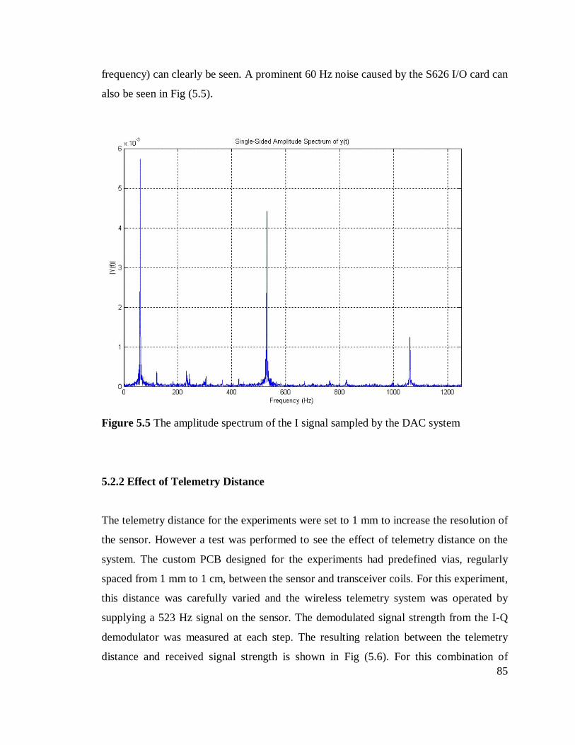
85
frequency) can clearly be seen. A prominent 60 Hz noise caused by the S626 I/O card can
also be seen in Fig (5.5).
Figure 5.5 The amplitude spectrum of the I signal sampled by the DAC system
5.2.2 Effect of Telemetry Distance
The telemetry distance for the experiments were set to 1 mm to increase the resolution of
the sensor. However a test was performed to see the effect of telemetry distance on the
system. The custom PCB designed for the experiments had predefined vias, regularly
spaced from 1 mm to 1 cm, between the sensor and transceiver coils. For this experiment,
this distance was carefully varied and the wireless telemetry system was operated by
supplying a 523 Hz signal on the sensor. The demodulated signal strength from the I-Q
demodulator was measured at each step. The resulting relation between the telemetry
distance and received signal strength is shown in Fig (5.6). For this combination of

86
system parameters, the maximum telemetry distance for a resolvable signal was
approximately 8 mm.
Figure 5.6 The effect of telemetry distance on the demodulated signal strength
5.2.3 Determination of the Frequency Response of the Capacitive MEMS Sensor
The wireless telemetry system was used to determine the frequency response of the
capacitive MEMS sensor. A frequency sweep from 10 Hz to 3 MHz was performed on
the membrane by using a frequency generator. The sinusoidal excitation had an
amplitude of 4V and a 5V DC-bias was supplied for bidirectional operation. The resulting
frequency response curve is shown in Fig (5.7).

87
Figure 5.7 The frequency response of the fabricated 500 µm capacitive membrane array
The resonant peak of the membranes’ dynamic response appears at 962.5 kHz, which is
above the calculated theoretical resonant frequency of 600kHz. This is thought to be due
a combination of factors such as the varying material properties of the deposited SiNx
membrane and the effect of the additional 5000 A° circumferential SiNx ring.
5.2.4 Capacitance Estimate by using the Proposed Cascaded Filter
The novel cascaded filter formulation for capacitance detection has been tested with the
capacitive sensor. For this experiment, a 10 V bias was applied and the membranes were
excited by a 5 V square wave at 523 Hz. The I and Q readings from the analog
demodulation circuitry were then digitized and the cascaded filter formulation was used
to calculate the MEMS sensor capacitance. The corresponding I, Q readings and the
estimated sensor capacitance are shown in Fig (5.8).

88
Figure 5.8 The passive wireless capacitance detection results through the implementation
of the cascaded filter
The cascaded filter successfully captures the pattern of change in sensor capacitance. The
frequency information is also preserved proving that the cascaded filter can be

89
implemented for high frequency measurements such as microphones. The results clearly
show the 523 Hz capacitance change. The measured change is around the nominal value
of approximately 4.2 pF. This is close to the calculated nominal capacitance of the
sensor. However with the applied bias the nominal value of the capacitance should be
approximately 4.5 pF. The error is believed to be caused by the inaccuracies in the model.
The spikes that appear in the measurements are due to noise in the sampled I and Q data.
5.3 Experimental Results by Using the SAW-IDT Pulse-Echo Type Modulation
The SAW sensors used in the experiments are designed to induce a time delay of 1 µs.
The center frequency of the devices was fixed at 99.5 MHz by designing the IDT finger
spacing correspondingly. Figure (5.9) shows the variation of the network reflection
parameter (S11) for the fabricated SAW-IDT sensors.
Figure 5.9 The variation in the network reflection parameter for the SAW-IDT sensors
The 0.5 MHz difference between the intended center frequency of 100 MHz and the
actual frequency is due to the small variation in IDT finger spacing during micro-
fabrication.

90
A typical pulse-echo type operation is shown in Fig (5.10). SAW-IDT interrogation pulse
width is 400 ns [Sezen et al. 2005].
Figure 5.10 Data showing the 400 ns SAW-IDT interrogation pulse and its reflection
The ratio of the amplitude of the reflected and interrogation pulses is a measure of
acoustic reflectivity. However, since the scaling of the acoustic reflectivity is irrelevant
for sensing the relative change in capacitance created by the sound wave, measurement of
the amplitude variations in the reflected pulse alone is sufficient. The experimental setup
used is depicted in Fig (5.11). In order to simulate a capacitive MEMS microphone, a
voltage-controlled capacitor (i.e. varactor) is used to mimic a condenser microphone
capacitance change.

91
Figure 5.11 Experimental setup for testing the varactor-controlled SAW-IDT sensor
[Sezen et al. 2005]
The amplitude of the reflected RF pulse is obtained by demodulation and reduced time-
domain sampling of the demodulated signal Reduced time domain sampling allows data
retrieval at relatively low sampling rates by extending the duration of the nanosecond
pulses using an intermediate analog sample-and-hold circuit before data acquisition,
which was designed specifically for the application [Sivaramakrishnan 2006].
To the best of the author’s knowledge, the detection of audio frequency signals is the first
high frequency sensing application of wireless SAW sensors. In order to verify the proof
of the outlined concepts, a high frequency voltage sensing application of SAW sensors
was implemented to detect digital audio signals using a voltage controlled capacitor
(varactor). The voltage-P11 relation was selected to mimic the relation between sound-
pressure and P11. The circuit implemented on the load IDT side is used to vary the
acoustic reflectivity by controlling the varactor capacitance. Different combinations of
sinusoidal signals as well as pre-recorded wave files were fed as input voltages. The time
domain and FFTs of the measured and input signals were used for analysis of the results,
which are shown in Fig. (5.12).

92
Figure 5.12 SAW-IDT telemetry experimental results a-) Comparison of the power
spectral density of the input and measured signals b-) Comparison of the original and
passive wirelessly retrieved signals [Sezen et al. 2005]
Experimental results show the transmitted signal experiencing wireless transmission and
losses in the SAW device before being received as the reflected signal. The amplitude of
the reflected signal shown in Fig (5.12) is attenuated by 14 dB. The maximum wireless
telemetry distance achieved by using two 100 MHz patch antennas was 7 cm. With a
telemetry distance of 4.5 cm, the sensitivity obtained was approximately 6 mV/pF. The
resolution at this distance was found to be 0.64 pF.

93
CHAPTER 6
CONCLUSION AND SUMMARY OF CONTRIBUTIONS
In this thesis, a novel approach to passive wireless sensing is described. Instead of
depending on bulky and expensive readout equipment, as in the case of the current
passive wireless sensing methods, the proposed method relies on real-time I-Q
demodulation of the current on the transceiver circuit and offers an inexpensive readout
achievable with a small readout setup. The most important contribution of the method
presented is that it enables passive wireless readout of high frequency sensor
measurements, which increases the breadth of the passive wireless sensing methods to
cover such high frequency sensors as microphones, ultrasound sensors, which was not
possible before, and any other sensor which will benefit from the readout of the high-
frequency components of measurement data.
In passive wireless sensing, the transceiver and receiver are relatively close to each other
compared to other forms of wireless telemetry. The received signal strength depends on
the quality of the mutual coupling between receiver and transceiver coil antennas, which
changes with the varying relative distance and angle of antennas. The changing mutual
coupling coefficient introduces another variable to the system in addition to the sensor
measurements. The fact that accurate modeling of the changing mutual coupling
coefficient is extremely challenging, renders straightforward calculation of the measured
data impossible.
This problem was resolved by developing novel algorithms to compensate for the effect
of the coupling coefficient as a result of the relative movement between the transceiver
and the sensor. The algorithms are based on real-time solution of a frequency domain
based mathematical model. These algorithms form a cascaded filter, which eliminates the
changing mutual coupling term from the system of equations. The sensor readout, usually
in the form of a capacitance change is then calculated without the need for the knowledge

94
of mutual coupling. By using the calculated capacitance value, it is also possible to find
the coupling coefficient. An improved version of the frequency domain system model
and the cascaded filter which consider high-frequency effects such as parasitic reactance
on the transceiver circuit have also been presented,.
This project also includes the development of a novel fabrication scheme that facilitates
the fabrication of capacitive MEMS sensors that are suitable to work with the proposed
passive wireless sensing scheme to form a miniature sensor package. Membrane-based
capacitive sensors were chosen because of the wide variety of applications that they can
be employed in, such as MEMS microphones, capacitive micromachined ultrasound
transducers, pressure sensors etc. There are unique requirements posed on a sensor used
in a passive wireless telemetry circuit. For capacitance-based passive wireless detection,
these translate into high sensitivity, low resistance and low parasitic capacitance of the
sensor. Although there are many examples of membrane based capacitive MEMS sensors
in the literature, there is a need for a fabrication strategy that focuses on satisfying all of
these requirements.
The capacitive MEMS sensors are fabricated by using surface micromachining from
PECVD deposited silicon nitride membranes and chromium-gold electrodes with
aluminum sacrificial layer. The concept of sandwiched metal layer has been introduced
for the first time for membrane-based sensors. This method involves the deposition of the
membrane in two steps. The top metallization layer is patterned in between these layers
and is “sandwiched” between the two parts of the membrane. In the literature, the
metallization is commonly placed on top of the membrane, which effectively increases
the capacitive gap and reduces the device sensitivity. The proposed fabrication strategy
will increase the capacitance and the electrical sensitivity of any capacitive membrane
based sensor regardless of the electrode area or capacitive air-gap hence introduces a
major improvement over existing strategies.

95
Two experimental batches of capacitive MEMS sensors have been fabricated. The first
batch of sensors had hexagonal membranes and as a result of the stress concentration at
their corners, membranes larger than 200 µm failed. In the second batch of the sensors
circular membrane designs were utilized. In the first trial of the second batch, despite the
fact that uniform stress was attained on the membranes, stress concentration at the very
edges of the membranes resulted in membrane dislocation. To resolve this problem a ring
of PECVD nitride is patterned along the circumference of the devices to strengthen the
edges and contain the stresses in the membrane.
As a result of these modifications, membranes ranging from 30 µm to 800 µm were
successfully fabricated on the same wafer. The fabricated MEMS sensors have been
integrated with the inductive coupling passive telemetry scheme to create a miniature
passive wireless sensor package that is capable of sensing high frequency measurements.
Experimental results show the successful operation of the passive wireless MEMS
package with the cascaded filter method, where the sensor capacitance change is at 523
Hz. The capacitance estimates given by the method show the varying capacitance
corresponding to the input excitation around a close estimate of the sensor nominal
capacitance. The mechanical frequency response of the MEMS sensor has also been
determined via the wireless telemetry link. The resonant peak of the sensor appears at
962.5 kHz which implies that this sensor, with proper modifications such as sealing the
etch holes, which were used to etch the sacrificial layer, could be used as a member of a
capacitive micromachined ultrasound transducer array.
A second method of passive wireless telemetry, SAW-IDT based telemetry has also been
investigated for high-frequency compatibility. A novel model for a passive wireless
microphone based on a SAW-IDT-MEMS sensor integration has been presented. The
experimental verification of the model was performed by using a varactor to mimic an
impedance changing capacitive MEMS microphone. By using the unique characteristics
of pulse-echo type modulation in SAW devices, it was possible to retrieve high frequency
data without any need for calibration.

96
BIBLIOGRAPHY
Akar O., Akin T., Najafi K., 2001, ‘A Wireless Batch Sealed Absolute Capacitive
Pressure Sensor’, Sensors and Actuators A, vol. 95, no. 1, pp. 29-38.
Akin T., Najafi K., Bradley R. M., 1998, ‘Wireless implantable multichannel digital
neural recording system for a micromachined sieve electrode’, IEEE Journal of Solid-
State Circuits, vol. 33, no. 1, pp. 109-118.
Allaert K., Calster A. V., 1985, 'A Comparison Between Silicon Nitride Films Made by
PECVD of N2-SiH4/Ar and N2-SiH4/He', Journal of Electrochemical Society-Solid-State
Science and Technology, vol.7 ,pp. 1763-1766
Allen M. G., 2005, ‘Micromachined endovascularly-implantable wireless aneurysm
pressure sensors: From concept to clinic’, 13th International Conference on Solid State
Sensors and Actuators and Microsystems, pp. 275-278.
Amjadi H., 2000, ‘Electret membranes and backelectrodes for application in
micromechanical transducers’, Journal of Electrostatics, vol. 48, pp. 179-191.
Baltes H., Paul O., Korvink J. G., 1996, ‘Simulation toolbox and material parameter
database for CMOS-MEMS’, IEEE Seventh International Symposium on Micro Machine
and Human Science, pp. 1-8.
Bao X.Q., Varadan V.V., Varadan V.K., 1987, ‘Saw temperature sensor and remote
reading system’, Ultrason. Symp. Proc., pp. 583-585.
Bilaniuk N., 1997, ‘Optical microphone transduction techniques’, Applied Acoustics, vol.
50, pp. 35-63.

97
Bogey R. A., Barnes L. A., Perry J., 1992, ‘Computer Algorithms to Characterize
Individual Subject EMG Profiles During Gait’, Arch. Phys. Med. Rehabil., vol. 73, pp.
835-841.
Bouroina T., Vauge C., Mekki H., 1995, ‘Variational method for tensile stress evaluation
and application to heavily boron-doped square-shaped silicon membranes”, Sensors and
Actuators A, vol. 49, pp. 21-27.
Butler J. C., Vigliotti A. J., Verdi F. W., Walsh S. M., 2002, ‘Wireless, passive resonant
circuit, inductively coupled inductive strain sensor’, Sensors and Actuators A, vol. 102,
pp. 61-66.
Caronti A., Caliano G., Carotenuto R., Savoia A., Pappalardo M., Cianci E., Foglietti V.,
2006, ‘Capacitive micromachined ultrasonic transducer (CMUT) arrays for medical
imaging’, Microelectronics Journal, vol. 37, no. 8, pp. 770-777.
Chatzandroulis S., Tsoukalas D., Neukomm P. A., 2000, ‘A miniature pressure system
with a capacitive sensor and a passive telemetry link for use in implantable applications”,
Journal of Microelectromechanical Systems, vol. 9, no. 1, pp. 18-23.
Chavan A., Wise K. D., 1997, ‘A batch processed vacuum-sealed capacitive pressure
sensor’, Proceedings of the 9th International Confenerence on Solid-State Sensors and
Actuators, Chicago-USA, pp. 1449-1452.
Close J. R., 1973, Functional Anatomy of the Extremities: Springfield.
Crenshaw A. G., Styf J. R., Hargens A. R., 1992, ‘Intramuscular pressures during
exercise: An evaluation of a fiberoptictransducer-tipped catheter system’, European
Journal of Applied Physiology, vol. 65, pp. 178-182.

98
Cho K. J., Asada H., 2002, ‘Wireless, battery-less stethoscope for wearable health
monitoring’, Bioengineering Conference, 2002.Proceedings of the IEEE 28th Annual
Northeast, pp. 187-188.
Chu J. H., Bak Y. H., Kang B. K., Kim U., Oum K. W., Choi J. G., Ko D. S., 1992,
‘Michelson interferometric detection for optoacoustic spectroscopy’, Optics
Communications, vol. 89, pp. 135-139.
Cunningham B. T., Bernstein J. J., 1997, ‘Wide-bandwidth silicon nitride membrane
microphones’, Proceedings of SPIE, Micromachining and Microfabrication Process
Technology III, vol. 3223, pp. 56-63.
Dell, J. M., Winchester, K., Musca, C. A., Antoszewski, J., Faraone L., 2002, ‘Variable
MEMS-based inductors fabricated from PECVD silicon nitride’, IEEE Proc. Conf. on
Optoelectron. and Microelectron. Mat. and Dev.(COMMAD 2002), Sydney, Australia,
pp. 567- 570.
Electret Microphone Turns 40. (n.d.) Retrieved October 2003 from
http://www.lucent.com/news_events/articles/020916.html
Fonseca M. A., English J. M., Von Arx M., Allen M. G., 2002, ‘Wireless micromachined
ceramic pressure sensor for high temperature applications’, Journal of
Microelectromechanical Systems, vol. 11, no. 4, pp. 337-343.
Gardner J. W., Varadan V. K., Awadelkarim O. O., 2001, Microsensors, MEMS, and
smart devices, Wiley, New York.
Gogoi B. P., Wang C. C., Mastrangelo C. H., 2001, ‘Force Balanced Micromachined
Pressure Sensors’, IEEE Transactions On Electron Devices, vol. 48, no. 8, 2001, pp.
1575-1584.

99
Grimes C. A., Cai Q., Ong K. G., Loiselle K., 2000, ‘Environmental monitoring using
magnetoelastic sensors’, Proceedings of SPIE - The International Society for Optical
Engineering, vol. 4097, pp. 123-133.
Grover F. W., 1946, Inductance Calculations, Van Nostrand, Princeton, NJ.
Harpster T.J., Stark B., Najafi K., 2001, ‘A Passive Wireless Integrated Humidity
Sensor’, The 14th IEEE International Conference on MEMS, pp. 553-557.
Hausleitner C., Steindl R., Pohl A., Brandl M., Seifert F., 2000, ‘State of the art radio
interrogation system for passive surface acoustic wave sensors’, Eurocomm 2000
IEEE/AFCEA, pp. 158-161.
Hill A. V., 1948, ‘The pressure developed in muscle during contraction’, J. Physiol., vol.
107, pp. 518-526.
Hill M., O'Mahony C., Duane R., Mathewson A., 2003, ‘Performance and reliability of
post-CMOS metal/oxide MEMS for RF application”, Journal of Micromechanics and
Microengineering, vol. 13, no. 4, pp. S131-S138.
Huang H. P., Liu C. P, 2006, ‘Design of combined voltage reference and temperature
sensor for RFID applications’, Sensor Review, vol. 26, no. 2, pp. 106-107.
Jin X., Ladabaum I., Degertekin F. L., Calmes S., Khuri-Yakub B. T., 1999, ‘Fabrication
and characterization of surface micromachined capacitive ultrasonic immersion
transducers’, IEEE Journal of Microelectromechanical Systems, vol. 8, no.1, pp. 100-
114.

100
King M., Phillips D. M., Zidulka A., Chang H. K., 1984, ‘Tracheal mucus clearance in
high frequency oscillation. II: Chest wall versus mouth oscillation”, American Rev.
Respiratory Disorders, vol. 130, no. 5, pp. 703-706.
Ko S.C., Kim Y. C., Lee S. S., Choi S. H., Kim S. R., 2003, ‘Micromachined
piezoelectric membrane acoustic device’, Sensors and Actuators A, vol. 103, pp. 130-
134.
Komi P. V., Rusko H., 1974, ‘Quantitative evaluation of mechanical and electrical
changes during fatigue loadings of eccentric and concentric work’, Scand. J. Rehabil. Med.,
Vol. 3 (Supplement), pp. 121-126.
Kovacs A., Stoffel A., 1994, ‘Mechanical analysis of polycrystalline and single-
crystalline silicon microstructures’, Sensors and Actuators A, vol 41, pp.672-679.
Kressmann R.., Klaiber M., Hess G., 2002, ‘Silicon condenser microphones with
corrugated silicon oxide/nitride membranes”, Sensors and Actuators A, vol. 100, pp. 301-
309.
Last M., Leibowitz B. S., Cagdaser B., Jog A., Zhou L., Boser B., Pister K. S. J., 2003,
‘Toward a wireless optical communication link between two small unmanned aerial
vehicles’, Proceedings - IEEE International Symposium on Circuits and Systems, vol. 3,
pp. III930-III933.
Lei M., Baldi A., Pan T., Gu Y., Siegel R. A., Ziaie B., 2004, ‘A hydrogel-based wireless
chemical sensor’, Proceedings of the 17th IEEE International Conference on Micro
Electro Mechanical Systems (MEMS), Maastricht MEMS 2004 pp. 391-394.
Lunnen J. D., Yack J., Le Veau B.F., 1981, ‘Relationship between muscle length, muscle
activity, torque of the hamstring muscles’, Phys. Ther., vol. 61, no. 2, pp. 190-195.

101
Lynch, J. P., John A. B., Law K. H., Kremidjian A. S., Carryer E.; Kenny T. W.,
Partridge A., Sundararajan A., 2002, ‘Validation of a wireless modular monitoring
system for structures’, Proceedings of SPIE - The International Society for Optical
Engineering, vol. 4696, pp. 124-135.
Martyniuk, M., Antoszewski, J., Musca, C.A., Dell, J.M., Faraone, L., 2004, ‘Stress
Response of Low Temperature PECVD Silicon Nitride Thin Films to Cryogenic Thermal
Cycling’, The IEEE Conference on Optoelectronic and Microelectronic Materials and
Devices, pp. 381-384.
Mazella H., 1954, ‘On the pressure developed by the contraction of striated muscle and its
influence on muscular circulation’, Archives of International Physiology, vol. 62, pp. 334-
347.
Miao J., Lin R., Chen L., Zou Q., Lim S. Y., Seah S. H., 2002, ‘Design considerations in
micromachined silicon microphones’, Microelectronics Journal, vol. 33, pp. 21-28.
Miki N., Shimoyama I., 2003, ‘Soft-magnetic rotational microwings in an alternating
magnetic field applicable to microflight mechanisms’, Journal of
Microelectromechanical Systems, vol. 12, no. 2, pp. 221-227.
Mullenborn M., Rombach P., Klein U., Rasmussen K., Kuhmann J. F., Heschel M.,
Amskov Gravad M., Janting J., Branebjerg J., Hoogerwerf A. C., Bouwstra S., 2001,
‘Chip-size-packaged silicon microphones’, Sensors and Actuators A, vol. 92, pp. 23-29.
Najafi K., 1995, ‘Recent progress in micromachining technology and application in
implantable biomedical systems’, IEEE Proceedings of the International Symposium on
Micromechatronics and Human Science, pp. 11-20.

102
Ning Y. B., Mitchell A. W., Tait R. N., 1996, ‘Fabrication of a silicon micromachined
capacitive microphone using a dry-etch process’, Sensors and Actuators A, vol. 53, pp.
237-242.
Noble R. A., Jones A. D. R., Robertson T. J., Hutchins D. A., Billson D. R., 2001,
‘Novel, Wide-bandwidth Micromachined Ultrasonic Transducers’, IEEE Transactions on
Ultrasonics, Ferroelectrics and Frequency Control, vol.48, No.6, pp. 1495-1507.
Norman R. W., Komi P. V., 1979, ‘Electromechanical delay in skeletal muscle under
normal movement conditions’, Acta Physiol. Scand., vol. 106, pp. 241-248.
Ong K. G., Grimes C. A., Robbins C. L., Singh R. S., 2001, ‘Design and application of a
wireless, passive, resonant circuit environmental monitoring sensor”, Sensors and
Actuators A, vol. 93, pp. 33-43.
Ong K. G., Puckett L. G., Sharma B. V., Loiselle M. G, Craig A., Bachas L. G., 2002,
‘Wireless passive resonant-circuit sensors for monitoring food quality’, Proceedings of
SPIE - Chemical and Biological Early Warning Monitoring for Water, Food, and
Ground, vol. 4575, pp. 150-159.
Randall J. N., Goldsmith C., Denniston D., Lin T. H., 1996, ‘Fabrication of
micromechanical switches for routing radio frequency signals’, Journal of Vacuum
Science and Technology, vol. 14, no. 6, pp. 3692-3696.
Reindl L., Ruile W., 1993, ‘Programmable reflectors for SAW-ID-tags’, Proc. IEEE
Ultrason. Symp., vol.1, pp. 125–130.
Ricciardi L., Pitz I., Al-Sarawi S. F., Varadan V., Abbott D., 2003, ‘Investigation into the
future of RFID in biomedical applications’, Proceedings of SPIE - The International
Society for Optical Engineering, vol. 5119, pp. 199-209.

103
Rosengren L., Backlundt V., Sjostromt T., Hokt B., Svedbergh B., 1992, 'A System for
wireless intra-ocular pressure measurements using a silicon micromachined sensor',
Journal of Micromechanics and Microengineering, vol. 2, pp. 202-204.
Rosentswieg J., Hinson M. M., 1972, ‘Comparison of isometric, isotonic, and isokinetic
exercises by electromyography’, Arch. Phys. Med. Rehabil., vol. 68, pp. 249-252.
Rothstein J. M., DeLitto A., Sinacore D. R., Rose S. J., 1983, ‘Electromyographic, peak
torque, and power relationships during isokinetic movement’, Phys. Ther, vol. 63, no. 6, pp.
926-933.
Royer M., Holmen J. O., Wurm M. A., Aadland O. S., Glenn M., 1983, ‘ZnO on Si
integrated acoustic sensor’, Sensors and Actuators, vol. 4, pp. 357-362.
Rudolf F., Bergqvist J., 1991, 'Silicon Micromachining for Sensor Applications',
Microelectronic Engineering, vol 15, pp. 399-406
Ruile W., 1994, “P-Matrix-Modelle von Oberflächenwellenbauelementen”, Ph.D.
dissertation, Dept. Elect. Eng. Info. Technol., Tech. Univ., Munich, Germany.
Sandeman E. K., 1983, Radio Engineering Volume I, Chapman & Hall Ltd., London, pp.
194-213.
Sejersted O. M., Hargens A. R., Kardel K. R., Blom P., Jensen O., Hermansen L. , 1984,
‘Intramuscular fluid pressure during isometric contraction of human skeletal muscle’, Journal
of Applied Physiology: Respiratory, Environmental & Exercise Physiology, vol. 56, no.
2, pp. 287-95.
Silver S., 1984, Microwave Antenna Theory and Design, Short Run Press Ltd., Exeter,
pp. 93-94.

104
Skolnik M. I., 1979, Introduction to Radar Systems, McGraw-Hill, New York.
Smidt G. L., 1973, ‘Biomechanial analysis of knee flexion and extension’, J.
Biomechanics, vol. 6, pp. 79-92.
Soh H. T., Ladabaum I., Atalar A., Quate C. F., Khuri-Yakub B. T., 1996, ‘Silicon
micromachined ultrasonic immersion transducers,’ Applied Physics Letters., vol. 69, no.
24, pp. 3674–3676.
Stangel K., Kolnsberg S., Hammerschmidt D., Hosticka B. J., Trieu H. K., Mokwa W.,
2001, ‘A Programmable intraocular CMOS pressure sensor system implant’, IEEE
Journal of Solid-State Circuits, vol. 36, no. 7, pp. 1094-1100.
Steindl R., Pohl A., and Seifert F., 1999, ‘Impedance loaded SAW sensors offer a wide
range of measurement opportunities’, IEEE Trans. MTT-S 1999, vol.47, no.12, pp. 2625-
2629.
Steindl R., Pohl A., Heinrich N., 2000, ‘Combination of SAW-transponder and RF-
semiconductor devices offers new perspectives for passive radio sensors’,
Eurocomm2000, pp. 162-165.
Subramanian H., Varadan V. K., Varadan V. V., Vellekopp M. J., 1997, ‘Design and
fabrication of wireless remotely readable MEMS based microaccelerometers’, Smart
Materials and Structures, vol. 6, pp. 730-738.
Suh W. D., Jose K. A., Xavier P. B., Varadan V. V., Varadan V. K., 2000, ‘Design
optimization and experimental verification of wireless IDT based micro temperature
sensor’, Smart Materials and Structures, vol. 9, pp. 890-897.

105
Sylvest O., Hvid N., 1959, ‘Pressure measurements in human striated muscles during
contraction’, Acta Rheumatoligica Scandanavica, vol. 5, pp. 216-222.
Tobolka, G., 1979, ‘Mixed matrix representation of SAW transducers’, IEEE
Transactions on Sonics and Ultrasonics, vol. 26, no.6.
Varadan V. K., 2002, ‘Wireless microsensors for health monitoring of structures’,
Proceedings of SPIE - The International Society for Optical Engineering, vol. 4935, pp.
526-536.
Varadan V. K., Teo P. T., Jose K. A., Varadan V. V., 2000, ‘Design and development of
a smart wireless system for passive temperature sensors’, Smart Materials and
Structures, vol. 9, pp. 379-388.
Varadan V. K., Varadan V. V., 2001, “Wireless surface acoustic wave and MEMS based
microsensors”, Proceedings of SPIE - The International Society for Optical Engineering,
vol. 4407, pp 256-266.
Varadan V. K., Vinoy K. J., Jose K. A., 2003, RF MEMS and Their Applications, John
Wiley & Sons, Ltd., West Sussex, pp. 180-193.
Vereecke G., Schaekers M., Verstraete K., Arnauts S., Heyns M., Plante W., 2000,
‘Quantitative Analysis of trace metals in Silicon Nitride Films by a Vapor Phase
Decomposition/Solution Collection Approach’, Journal of Electrochemical. Society, vol.
147, no.4, pp. 1499-1501.
Viktorov, I. A., 1967, Rayleigh and Lamb Waves: Physical Theory and Applications,
Plenum Press, New York.

106
Von Arx J. A., Najafi K., 1997, ‘On-chip coils with integrated cores for remote inductive
powering of integrated microsystems’, IEEE International Conference on Solid-State
Sensors and Actuators, Proceedings, vol. 2, pp. 999-1002.
Warwick W. J., Hansen L. G., 1991, ‘The long term effect of high frequency chest
compression therapy on pulmonary complications of cystic fibrosis’, Pediatric
Pulmonology, vol.11, no. 3, pp. 265-271.
Warwick W., Personal communication, 2003.
Watters, D. G., Jayaweera, P., Bahr, A. J., Huestis, D. L., 2002, ‘Design and performance
of wireless sensors for structural health monitoring’, Quantitative Nondestructive
Evaluation AIP Conference Proceedings, vol. 615, pp. 969-976.
Willinger M., James L. S., Catz C., 1991, ‘Defining the sudden infant death syndrome
(SIDS): deliberations of an expert panel convened by the National Institute of Child
Health and Human Development’, Pediatric Pathology, vol. 11, no.5, pp. 677-684.
Winchester, K. J. and Dell, J. M., 2001, ‘Tunable Fabry-Pérot cavities fabricated from
PECVD silicon nitride employing zinc sulphide as the sacrificial layer’, J. Micromech.
Microeng., vol. 11, pp. 589-596
Yesin K. B., Exner P., Vollmers K., Nelson B. J., 2005, ‘Design and Control of In-Vivo
Magnetic Microrobots’, Proc. 8th International Conference on Medical Image
Computing and Computer Assisted Intervention (MICCAI), Palm Springs, USA.
Zhang H., Laws A., Gupta K. C., Lee Y. C., Bright V. M., 2003, ‘MEMS-Variable
Capacitor Phase Shifters Part I: Loaded-line Phase Shifter’, International Journal of RF
and Microwave Computer-Aided Engineering, vol. 13, no. 4, pp. 321-337.


