

VITA 62 DC-DC Converter Rev 1.1Page 1 of 26 06/2019
VITA 62 DC-DC Converter
VITA 62 Power SupplyVIT028wxx600yzzz
Note: Product images may not highlight current product markings.
Features & Benefits
• Open VPX – VITA 62
• 18 – 50V input voltage range
• 600W output power
• 3U Open VPX power supply
• Conduction cooled
• 6 outputs
• I2C™ monitoring and control
• Input voltage reverse-polarity protection
• Remote voltage sense: VS1, VS2, VS3
• Parallel operation capable with proprietary wireless current sharing
• Overcurrent, overvoltage and overtemperature protections
• IPC 610 class 3
• No aluminum electrolytic capacitors
• Enable, inhibit, system reset and power fail controls
• Military standard compliance: [a]
�� MIL-STD-704F (Pending)�� MIL-STD-461F�� MIL-STD-810G�� MIL-STD-1275D Normal Surges and Spikes�� RTCA/DO-160G
Typical Applications
• VPX power modules
• Avionics
• Shipborne electronics
Product Description
The Vicor VITA 62 power supply is a COTs power supply that is designed for 3U Open VPX systems. The module utilizes Vicor proprietary technology to enable high efficiency and power density for this highly rugged, conduction-cooled model.
Up to four power supplies can be paralleled to increase output power capability of VS1, VS2, VS3 outputs with proprietary wireless current sharing. Conventional current-share pins are eliminated. Current share accuracy is ±1A.
[a] See detailed specifications

VITA 62 DC-DC Converter Rev 1.1Page 2 of 26 06/2019
VIT028wxx600yzzz
3U P0 Connector
P1 P2 LP1
1 2 3 4 5 6 7 8
P3 P4 P5 LP2 P6
ROWSSIGNAL
POWER POWER
DCBA
Connector Pin Configuration
Note: See mechanical drawing on page 17 for connector information.
VITA 62 DC-DC Converter Rev 1.1Page 3 of 26 06/2019
VIT028wxx600yzzz
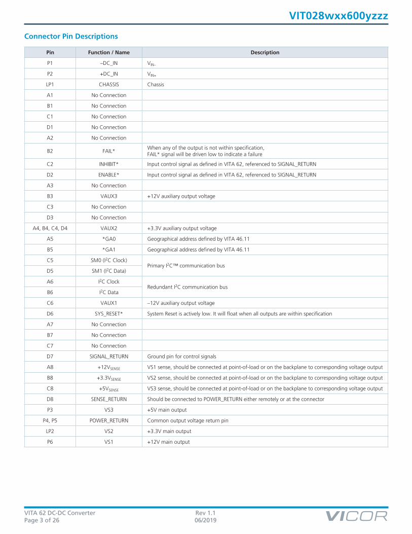
Connector Pin Descriptions
Pin Function / Name Description
P1 –DC_IN VIN–
P2 +DC_IN VIN+
LP1 CHASSIS Chassis
A1 No Connection
B1 No Connection
C1 No Connection
D1 No Connection
A2 No Connection
B2 FAIL*When any of the output is not within specification, FAIL* signal will be driven low to indicate a failure
C2 INHIBIT* Input control signal as defined in VITA 62, referenced to SIGNAL_RETURN
D2 ENABLE* Input control signal as defined in VITA 62, referenced to SIGNAL_RETURN
A3 No Connection
B3 VAUX3 +12V auxiliary output voltage
C3 No Connection
D3 No Connection
A4, B4, C4, D4 VAUX2 +3.3V auxiliary output voltage
A5 *GA0 Geographical address defined by VITA 46.11
B5 *GA1 Geographical address defined by VITA 46.11
C5 SM0 (I2C Clock)Primary I2C™ communication bus
D5 SM1 (I2C Data)
A6 I2C ClockRedundant I2C communication bus
B6 I2C Data
C6 VAUX1 –12V auxiliary output voltage
D6 SYS_RESET* System Reset is actively low. It will float when all outputs are within specification
A7 No Connection
B7 No Connection
C7 No Connection
D7 SIGNAL_RETURN Ground pin for control signals
A8 +12VSENSE VS1 sense, should be connected at point-of-load or on the backplane to corresponding voltage output
B8 +3.3VSENSE VS2 sense, should be connected at point-of-load or on the backplane to corresponding voltage output
C8 +5VSENSE VS3 sense, should be connected at point-of-load or on the backplane to corresponding voltage output
D8 SENSE_RETURN Should be connected to POWER_RETURN either remotely or at the connector
P3 VS3 +5V main output
P4, P5 POWER_RETURN Common output voltage return pin
LP2 VS2 +3.3V main output
P6 VS1 +12V main output
VITA 62 DC-DC Converter Rev 1.1Page 4 of 26 06/2019
VIT028wxx600yzzz
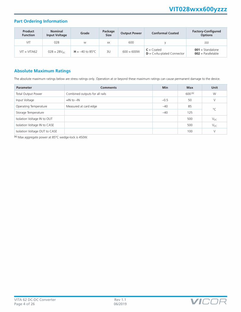
Part Ordering Information
ProductFunction
Nominal Input Voltage
GradePackage
SizeOutput Power Conformal Coated
Factory-Configured Options
VIT 028 w xx 600 y zzz
VIT = VITA62 028 = 28VDC H = –40 to 85ºC 3U 600 = 600W C = Coated D = C+Au-plated Connector
001 = Standalone002 = Parallelable
Absolute Maximum Ratings
The absolute maximum ratings below are stress ratings only. Operation at or beyond these maximum ratings can cause permanent damage to the device.
Parameter Comments Min Max Unit
Total Output Power Combined outputs for all rails 600 [b] W
Input Voltage +IN to –IN –0.5 50 V
Operating Temperature Measured at card edge –40 85ºC
Storage Temperature –40 125
Isolation Voltage IN to OUT 500 VDC
Isolation Voltage IN to CASE 500 VDC
Isolation Voltage OUT to CASE 100 V
[b] Max aggregate power at 85ºC wedge-lock is 450W.
VITA 62 DC-DC Converter Rev 1.1Page 5 of 26 06/2019
VIT028wxx600yzzz
Electrical Characteristics
All data at nominal line and nominal load unless otherwise specified.
Attribute Symbol Conditions / Notes Min Typ Max Unit
Overall System Characteristics
System Efficiency
Nominal line, 20% aggregate loads 71
%Nominal line, 50% aggregate loads 84.8
Nominal line, 100% aggregate loads 87.5
Power Input Characteristics
Operating Input Voltage Range VIN 18 28 50 V
Input Current (No Load) IIN-NL 28V Input, enable asserted, inhibit de-asserted 0.43 0.60 A
Inrush Current IINRUSHPeak no load, nominal line, high line; see Figures 22, 23
400 830 A
Input Undervoltage Protection Threshold
VUV-IN 1ms response time 17.5 V
Input Overvoltage Protection Threshold
VOV-IN 1ms response time 50.5 V
Power On to +3.3VAUX Output Delay If EN* is tied to signal ground 200 250 400 ms
Main Outputs
VS1: +12V Output
Output Voltage Set Point [c]Standalone 11.90 12 12.1
VParallel, droop share 11.80 12.1
Output Regulation Over Line & LoadStandalone 100 200
mVParallel 150 250
Output Voltage Ripple / Noise Nominal line from 2A load to full load 120 mVP-P
Output Overcurrent Protection IOC-S-VS1 2Hz filter on OCP 45 A
Output Overvoltage Protection VOV-S-VS1 2Hz filter on OVP 12.6 V
Output Undervoltage Protection VUV-S-VS1 2Hz filter on UVP 11.4 V
Rated Output Current IR-VS1 40 A
Output Power limit PLIM-F-VS1
1ms response time; power calculation includes transmission voltage drop; enabled 5ms after voltage output is enabled
480 W
Fast Overcurrent Protection Limit IOC-F-VS11ms response time; enabled 5ms after voltage output is enabled
40 45 52 A
Maximum Operating Transmission Voltage Drop
VTD-VS1 0.6 V
Maximum Output Capacitance CO-VS1 9 mF
Soft-Start Ramp Time tSS-VS1 All full load with max CO-VS1 5 ms

VITA 62 DC-DC Converter Rev 1.1Page 6 of 26 06/2019
VIT028wxx600yzzz
Attribute Symbol Conditions / Notes Min Typ Max Unit
Main Outputs (Cont.)
VS3: +5V Output
Output Voltage Set Point [c]Standalone 4.95 5 5.05
VParallel, droop share 4.9 5.1
Output Regulation Over Line & LoadStandalone 50 100
mVParallel 100 150
Output Voltage Ripple / NoiseNominal line over load range, 20MHz BW; measured with 1µF and 10µF ceramic capacitor
50 mVP-P
Output Overcurrent Protection IOC-S-VS3 2Hz filter on OCP 30 32 A
Output Overvoltage Protection VOV-S-VS3 2Hz filter on OVP 5.15 V
Output Undervoltage Protection VUV-S-VS3 2Hz filter on UVP 4.9 V
Rated Output Current IR-VS3 30 A
Output Power limit PLIM-F-VS3
1ms response time; power calculation includes remote-sense voltage drop; enabled 5ms after voltage output is enabled
150 W
Fast Overcurrent Protection Limit IOC-F-VS31ms response time; enabled 5ms after voltage output is enabled
30 32 35 A
Maximum Operating Transmission Voltage Drop
VTD-VS3 0.6 V
Maximum Output Capacitance CO-VS3 9 mF
Soft-Start Ramp Time tSS-VS3 All full load with max CO-VS3 5 ms
VS2: +3.3V Output
Output Voltage Set Point [c]Standalone
3.25 3.35 3.45 VParallel, droop share
Output Regulation Over Line & LoadStandalone 50 100
mVParallel 100 150
Output Voltage Ripple / NoiseNominal line over load range, 20MHz BW; measured with 1µF and 10µF ceramic capacitor
50 mVP-P
Output Overcurrent Protection IOC-S-VS2 2Hz filter on OCP 35 A
Output Overvoltage Protection VOV-S-VS2 2Hz filter on OVP 3.5 V
Output Undervoltage Protection VUV-S-VS2 2Hz filter on UVP 3.2 V
Rated Output Current IR-VS2 20 A
Output Power limit PLIM-F-VS2
1ms response time; power calculation includes remote-sense voltage drop; enabled 5ms after voltage output is enabled
82 W
Fast Overcurrent Protection Limit IOC-F-VS21ms response time; enabled 50ms after voltage output is enabled
24 30 40 A
Maximum Operating Transmission Voltage Drop
VTD-VS2 0.6 V
Maximum Output Capacitance CO-VS2 9 mF
Soft-Start Ramp Time tSS-VS2 All full load with max CO-VS3 50 ms
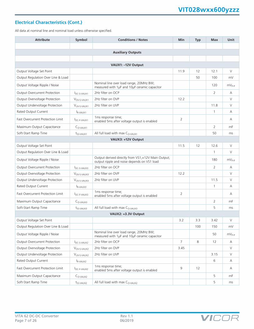
Electrical Characteristics (Cont.)
All data at nominal line and nominal load unless otherwise specified.
[c] 50% load.
VITA 62 DC-DC Converter Rev 1.1Page 7 of 26 06/2019
VIT028wxx600yzzz
Attribute Symbol Conditions / Notes Min Typ Max Unit
Auxiliary Outputs
VAUX1: –12V Output
Output Voltage Set Point 11.9 12 12.1 V
Output Regulation Over Line & Load 50 100 mV
Output Voltage Ripple / NoiseNominal line over load range, 20MHz BW; measured with 1µF and 10µF ceramic capacitor
120 mVP-P
Output Overcurrent Protection IOC-S-VAUX1 2Hz filter on OCP 2 A
Output Overvoltage Protection VOV-S-VAUX1 2Hz filter on OVP 12.2 V
Output Undervoltage Protection VUV-S-VAUX1 2Hz filter on UVP 11.8 V
Rated Output Current IR-VAUX1 1 A
Fast Overcurrent Protection Limit IOC-F-VAUX11ms response time; enabled 5ms after voltage output is enabled
2 A
Maximum Output Capacitance CO-VAUX1 2 mF
Soft-Start Ramp Time tSS-VAUX1 All full load with max CO-VAUX1 50 ms
VAUX3: +12V Output
Output Voltage Set Point 11.5 12 12.6 V
Output Regulation Over Line & Load 1 V
Output Voltage Ripple / NoiseOutput derived directly from VS1,+12V Main Output; output ripple and noise depends on VS1 load
180 mVP-P
Output Overcurrent Protection IOC-S-VAUX3 2Hz filter on OCP 2 A
Output Overvoltage Protection VOV-S-VAUX3 2Hz filter on OVP 12.2 V
Output Undervoltage Protection VUV-S-VAUX3 2Hz filter on UVP 11.5 V
Rated Output Current IR-VAUX3 1 A
Fast Overcurrent Protection Limit IOC-F-VAUX31ms response time; enabled 5ms after voltage output is enabled
2 A
Maximum Output Capacitance CO-VAUX3 2 mF
Soft-Start Ramp Time tSS-VAUX3 All full load with max CO-VAUX3 5 ms
VAUX2: +3.3V Output
Output Voltage Set Point 3.2 3.3 3.42 V
Output Regulation Over Line & Load 100 150 mV
Output Voltage Ripple / NoiseNominal line over load range, 20MHz BW; measured with 1µF and 10µF ceramic capacitor
50 mVP-P
Output Overcurrent Protection IOC-S-VAUX2 2Hz filter on OCP 7 8 12 A
Output Overvoltage Protection VOV-S-VAUX2 2Hz filter on OVP 3.45 V
Output Undervoltage Protection VUV-S-VAUX2 2Hz filter on UVP 3.15 V
Rated Output Current IR-VAUX2 6 A
Fast Overcurrent Protection Limit IOC-F-VAUX21ms response time; enabled 5ms after voltage output is enabled
9 12 A
Maximum Output Capacitance CO-VAUX2 5 mF
Soft-Start Ramp Time tSS-VAUX2 All full load with max CO-VAUX2 5 ms
Electrical Characteristics (Cont.)
All data at nominal line and nominal load unless otherwise specified.

VITA 62 DC-DC Converter Rev 1.1Page 8 of 26 06/2019
VIT028wxx600yzzz
Agg
rega
te O
utpu
t Pow
er (W
)
Temperature (ºC)
400
450
500
550
600
650
50 60 70 80 9085756555
Net
Out
put P
ower
(W)
Temperature (ºC)
400
450
500
550
600
650
50 60 70 80 9085756555
Figure 1 — Thermal specified operating area: aggregate power vs. rail temperature for power‑limited operation
Figure 2 — Thermal specified operating area: worst‑case loading vs. rail temp for power‑limited operation Load configuration: VS1 @ 40A, VAUX1 @ 1A,
Constant 525W
VAUX2 @ 6A, VAUX3 @ 1A Remaining outputs loaded on aggregate to achieve 600W combined output below 70ºC rail temperature
Operating Area
}
VITA 62 DC-DC Converter Rev 1.1Page 9 of 26 06/2019
VIT028wxx600yzzz
Signal Characteristics
All of the following plots are at nominal line and 600W aggregate load unless otherwise noted.
EN*: Enable*
• The EN* pin or control register bit enables and disables the +3.3V AUX output of the power supply.• The EN* pin has an internal pull-up to VCC and is referenced to the Signal Return pin of the power supply.
Signal Type State Attribute Symbol Conditions / Notes Min Typ Max Unit
Digital Input
Any
EN* Enable Threshold VENABLE-EN 0.8 V
EN* Disable Threshold VENABLE-DIS 2.0 V
Internally Generated VCC VCC 3.21 3.30 3.39 V
EN* Internal Pull-Up Resistance to VCC
RENABLE-INT 49 51 52 kΩ
EN* Enable Debounce Delay
tD-EN-E 40 100 150 ms
EN* Disable Debounce Delay
tD-EN-D 40 100 150 ms
IN*: Inhibit*
• The IN* pin enables and disables all outputs except +3.3VAUX if VENABLE-EN threshold has been met.• The IN* pin has an internal pull up to VCC and is referenced to the Signal Return pin of the power supply.
Signal Type State Attribute Symbol Conditions / Notes Min Typ Max Unit
Digital Input
Any
IN* Enable Threshold VINHIBIT-EN Status register bit 4 should be 0 (default) for digital input control line to have priority
2.0 V
IN* Disable Threshold VINHIBIT-DIS 0.8 V
Internally Generated VCC VCC 3.21 3.30 3.39 V
IN* Internal Pull-Up Resistance to VCC
RDISABLE-INT 49 51 52 kΩ
IN* Enable Debounce Delay after EN*
tD-IN-E 300 500 700 ms
IN* Disable Debounce Delay
tD-IN-D 10 40 100 ms
Lockout Delay Between Consecutive IN* Enables
tD-IN-L 100 300 ms
VITA 62 DC-DC Converter Rev 1.1Page 10 of 26 06/2019
VIT028wxx600yzzz
Signal Characteristics (Cont.)
All of the following plots are at nominal line and 600W aggregate load unless otherwise noted.
GA0*, GA1*: Global Address
• The GA0* and GA1* pins sets the I2C™ address of the power supply. Global address is set at start up and cannot be changed without a power cycle.• The GA0* and GA1* pins have an internal pull-up to VCC and is referenced to the Signal Return pin of the power supply.
Signal Type State Attribute Symbol Conditions / Notes Min Typ Max Unit
Digital Input
Start Up
Address Pins Low Threshold
VADDR-L 0.8 V
Address Pins High Threshold
VADDR-H 2.0 V
Internally Generated VCC VCC 3.21 3.30 3.39 V
EN* Internal Pull-Up Resistance to VCC
RADDR-INT 49 51 52 kΩ
Address Pins Debounce Delay
tD-ADDR 5 25 ms
FAIL*, SYSRESET* & LED
• The power supply has one two color LED located on the ejector edge of the power supply.• The LED is either GREEN or RED depending on the state of operation. FAIL* and SYSRESET* lines are set with the LED.
Signal Type State Attribute Symbol Conditions / Notes Min Typ Max Unit
Outputs
Steady RED
SYSRESET* VSYSRSTStart up: input voltage operating threshold VUV-IN < VIN < VOV-IN has been met; if steady RED persists for >100ms, a critical system fault has been detected during start up
0.0 0.1 0.8 V
FAIL* VFAIL 0.0 0.1 0.8 V
Blinking GREEN
SYSRESET* VSYSRST >100ms after VUV-IN < VIN < VOV-IN has been met; power supply is ready for use
2.0 3.2 3.4 V
FAIL* VFAIL 2.0 3.2 3.4 V
Steady GREEN
SYSRESET* VSYSRSTAll outputs are OK and EN* is pulled low
2.0 3.2 3.4 V
FAIL* VFAIL 2.0 3.2 3.4 V
Blinking RED
SYSRESET* VSYSRST Power supply has encountered a OT, OV, UV, OC or critical system failure during operating
2.0 3.2 3.4 V
FAIL* VFAIL 0.0 0.1 0.8 V
VITA 62 DC-DC Converter Rev 1.1Page 11 of 26 06/2019
VIT028wxx600yzzz
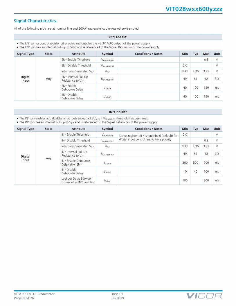
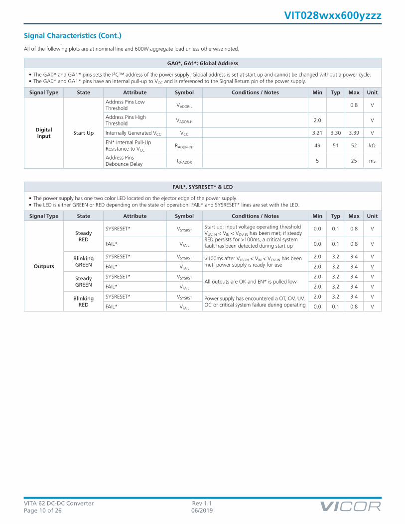
Application Characteristics
All of the following plots are at nominal line and 600W aggregate load unless otherwise noted.
Figure 3 — Delay between application of input power and all outputs available; ENABLE tied to signal ground and INHIBIT left floating
Figure 5 — Delay between ENABLE line transitioning from floating to signal ground and all outputs becoming available; INHIBIT left floating
Figure 4 — Delay between removal of input power and all outputs decaying; ENABLE tied to signal ground and INHIBIT left floating
Figure 6 — Delay between ENABLE line transitioning from signal ground to floating and all outputs decaying; INHIBIT left floating
–0.5 –0.25 0 0.25 0.5 0.75 1 1.25 1.5 1.75 2
Time (s)
–12.0
03.355.0
12.0
28.0
Volta
ge (V
)
VAUX3
VAUX1
VAUX2
VIN
VS1
VS2
VS3
–0.2 –0.1 0 0.1 0.2 0.3 0.4 0.5 0.6 0.7 0.8
Time (s)
–12.0
03.355.0
12.0
28.0
Volta
ge (V
)
VAUX3
VAUX1
VAUX2
VIN
ENABLE
VS1
VS2
VS3
–0.5 –0.25 0 0.25 0.5 0.75 1 1.25 1.5 1.75 2
Time (s)
–12.0
03.355.0
12.0
28.0
Volta
ge (V
)
VAUX3
VAUX1
VAUX2
VIN
VS1
VS2
VS3
–0.2 –0.1 0 0.1 0.2 0.3 0.4 0.5 0.6 0.7 0.8
Time (s)
–12.0
03.355.0
12.0
28.0Vo
ltage
(V)
VAUX3
VAUX1
VAUX2
VIN
ENABLE
VS1
VS2
VS3

VITA 62 DC-DC Converter Rev 1.1Page 12 of 26 06/2019
VIT028wxx600yzzz
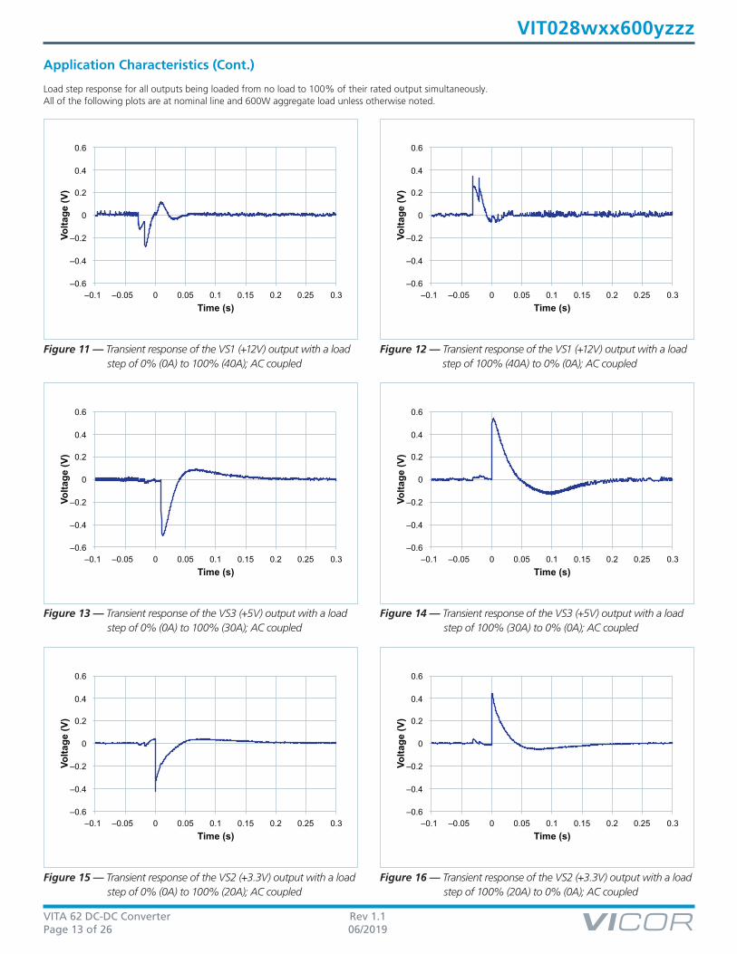
Application Characteristics (Cont.)
All of the following plots are at nominal line and 600W aggregate load unless otherwise noted.
Figure 7 — Delay between INHIBIT line transitioning from floating to signal ground and corresponding outputs decaying; VAUX2 (+3.3V) remains on; ENABLE tied to signal ground
Figure 8 — Time delay between INHIBIT line transitioning from signal ground to floating and corresponding outputs becoming available; VAUX2 (+3.3V) remains on; ENABLE tied to signal ground
–0.2 –0.1 0 0.1 0.2 0.3 0.4 0.5 0.6 0.7 0.8
Time (s)
–12.0
03.355.0
12.0
28.0
Volta
ge (V
)
VAUX3
VAUX1
VAUX2
VIN
INHIBIT
VS1
VS2
VS3
–0.2 –0.1 0 0.1 0.2 0.3 0.4 0.5 0.6 0.7 0.8
Time (s)
–12.0
03.355.0
12.0
28.0
Volta
ge (V
)
VAUX3
VAUX1
VAUX2
VIN
INHIBIT
VS1
VS2
VS3
Figure 10 — Inrush current at max input voltage (45V); CH1 – inrush current, 1mV/A; CH2 – card input voltage
Figure 9 — Inrush current at nominal input voltage; CH1 – inrush current, 1mV/A; CH2 – card input voltage
Time (ms)
Inru
sh C
urre
nt (A
)
Car
d In
put V
olta
ge (V
)
0 0
200
400
600
–200
12
–12
24
48
36
60
800
1000
–0.5 0 0.5 1 1.5 2
VIN IINRUSH
Time (ms)
Inru
sh C
urre
nt (A
)
Car
d In
put V
olta
ge (V
)
0 0
100
200
300
400
6
12
18
24
30500
–0.5 0 0.5 1 1.5 2
VIN IINRUSH
VITA 62 DC-DC Converter Rev 1.1Page 13 of 26 06/2019
VIT028wxx600yzzz
Figure 12 — Transient response of the VS1 (+12V) output with a load step of 100% (40A) to 0% (0A); AC coupled
Figure 11 — Transient response of the VS1 (+12V) output with a load step of 0% (0A) to 100% (40A); AC coupled
Time (s)
Volta
ge (V
)
0
0.2
0.4
0.6
–0.1 –0.05 0 0.05 0.1 0.15 0.2 0.25 0.3–0.6
–0.4
–0.2
Time (s)
Volta
ge (V
)
0
0.2
0.4
0.6
–0.1 –0.05 0 0.05 0.1 0.15 0.2 0.25 0.3–0.6
–0.4
–0.2
Application Characteristics (Cont.)
Load step response for all outputs being loaded from no load to 100% of their rated output simultaneously. All of the following plots are at nominal line and 600W aggregate load unless otherwise noted.
Figure 16 — Transient response of the VS2 (+3.3V) output with a load step of 100% (20A) to 0% (0A); AC coupled
Time (s)
Volta
ge (V
)
0
0.2
0.4
0.6
–0.1 –0.05 0 0.05 0.1 0.15 0.2 0.25 0.3–0.6
–0.4
–0.2
Figure 15 — Transient response of the VS2 (+3.3V) output with a load step of 0% (0A) to 100% (20A); AC coupled
Time (s)
Volta
ge (V
)
0
0.2
0.4
0.6
–0.1 –0.05 0 0.05 0.1 0.15 0.2 0.25 0.3–0.6
–0.4
–0.2
Figure 13 — Transient response of the VS3 (+5V) output with a load step of 0% (0A) to 100% (30A); AC coupled
Figure 14 — Transient response of the VS3 (+5V) output with a load step of 100% (30A) to 0% (0A); AC coupled
Time (s)
Volta
ge (V
)
–0.6
–0.4
–0.2
0
0.2
0.4
0.6
–0.1 –0.05 0 0.05 0.1 0.15 0.2 0.25 0.3Time (s)
Volta
ge (V
)
0
0.2
0.4
0.6
–0.1 –0.05 0 0.05 0.1 0.15 0.2 0.25 0.3–0.6
–0.4
–0.2
VITA 62 DC-DC Converter Rev 1.1Page 14 of 26 06/2019
VIT028wxx600yzzz
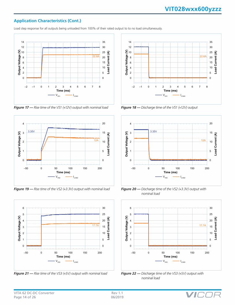
Figure 22 — Discharge time of the VS3 (+5V) output with nominal load
Figure 21 — Rise time of the VS3 (+5V) output with nominal load
Time (ms)
Out
put V
olta
ge (V
)
Load
Cur
rent
(A)
0 0
1
2
4
3
5
10
30
25
20
15
6
5
–50 0 50 150 200100
17.7A
VVS3 ILOAD
Time (ms)
Out
put V
olta
ge (V
)
Load
Cur
rent
(A)
0 0
1
2
4
3
5
10
30
25
20
15
6
5
–50 0 50 150 200100
17.7A
VVS3 ILOAD
Application Characteristics (Cont.)
Load step response for all outputs being unloaded from 100% of their rated output to to no load simultaneously.
Figure 17 — Rise time of the VS1 (+12V) output with nominal load Figure 18 — Discharge time of the VS1 (+12V) output
Time (ms)
Out
put V
olta
ge (V
)
Load
Cur
rent
(A)
0 0
2
4
6
8
10
12
5
10
20
15
30
25
3514
–2 –1 0 2 3 4 51 6 7 8
22.6A
VVS1 ILOAD
Time (ms)
Out
put V
olta
ge (V
)
Load
Cur
rent
(A)
0 0
2
4
6
8
10
12
5
10
20
15
30
25
3514
–2 –1 0 2 3 4 51 6 7 8
22.6A
VVS1 ILOAD
Figure 20 — Discharge time of the VS2 (+3.3V) output with nominal load
Figure 19 — Rise time of the VS2 (+3.3V) output with nominal load
Time (ms)
Out
put V
olta
ge (V
)
Load
Cur
rent
(A)
0 0
1
2
3
5
10
20
15
4
–50 0 50 150 200100
12A
3.35V
VVS2 ILOAD
Time (ms)
Out
put V
olta
ge (V
)
Load
Cur
rent
(A)
0 0
1
2
3
5
10
20
15
4
–50 0 50 150 200100
12A
3.35V
VVS2 ILOAD

VITA 62 DC-DC Converter Rev 1.1Page 15 of 26 06/2019
VIT028wxx600yzzz
Figure 28 — Discharge time of the VAUX2 (+3.3V) output with nominal load
Figure 27 — Rise time of the VAUX2 (+3.3V) output with nominal load
Time (ms)
Out
put V
olta
ge (V
)
Load
Cur
rent
(A)
0.5
0
1
0
1
1.5
2.5
2
2
3
7
8
6
5
4
3.5
4
3
–5 –2.5 2.50 5 7.5 1510 12.5
3.35V
VVAUX2 ILOAD
Time (ms)
Out
put V
olta
ge (V
)
Load
Cur
rent
(A)
0.5
0
1
0
1
1.5
2.5
2
2
3
7
8
6
5
4
3.5
4
3
–5 –2.5 2.50 5 7.5 1510 12.5
3.35V
VVAUX2 ILOAD
Application Characteristics (Cont.)
Load step response for all outputs being unloaded from 100% of their rated output to to no load simultaneously.
Figure 23 — Rise time of the VAUX1 (–12V) output with nominal load Figure 24 — Discharge time of the VAUX1 (–12V) output
Time (ms)
Out
put V
olta
ge (V
)
Load
Cur
rent
(A)
2
0
–2
0.5
0
–0.5
4
6
10
8
1
1.5
3.5
3
2.5
2
14
12
–20 –10 100 20 30 60 70 8040 50
0.75A
VVAUX3 ILOAD
Time (ms)
Out
put V
olta
ge (V
)
Load
Cur
rent
(A)
2
0
–2
0.5
0
–0.5
4
6
10
8
1
1.5
3.5
3
2.5
2
14
12
–20 –10 100 20 30 60 70 8040 50
0.75A
VVAUX3 ILOAD
Figure 26 — Discharge time of the VAUX3 (+12V) output with nominal load
Figure 25 — Rise time of the VAUX3 (+12V) output with nominal load
Time (ms)
Out
put V
olta
ge (V
)
Load
Cur
rent
(A)
–10
–12
–14
–2.5
–3
–3.5
–8
–6
–2
–4
–2
–1.5
0.5
0
–0.5
–1
2
0
–20 –10 100 20 30 60 70 8040 50
–0.75A
VVAUX1 ILOAD
Time (ms)
Out
put V
olta
ge (V
)
Load
Cur
rent
(A)
–10
–12
–14
–2.5
–3
–3.5
–8
–6
–2
–4
–2
–1.5
0.5
0
–0.5
–1
2
0
–20 –10 100 20 30 60 70 8040 50
–0.75A
VVAUX1 ILOAD

VITA 62 DC-DC Converter Rev 1.1Page 16 of 26 06/2019
VIT028wxx600yzzz
Attribute Symbol Conditions / Notes Min Typ Max Unit
Mechanical
Length L Per VITA62 6.634 in
Width W Per VITA62 3.937 in
Height H Per VITA62 0.951 in
Weight W 635 g
Wedge-Lock Torque Manufacturer’s recommended value 7 in.lbs
Thermal
Operating Temperature TWEDGE-LOCKS –40 85 °C
Assembly
Storage Temperature –40 125 ºC
Safety
MTBF
MIL-HDBK-217Plus Parts Count - 25°C Ground Benign, Stationary, Indoors / Computer
TBD Hrs
Telcordia Issue 2 - Method I Case III; 25°C Ground Benign, Controlled
TBD Hrs
General Characteristics

VITA 62 DC-DC Converter Rev 1.1Page 17 of 26 06/2019
VIT028wxx600yzzz
GA0*
SW
10kΩ
VCC
GA1*
Vcc
SYSRESET*
50kΩ
From IPMC
To IPMC
50kΩ
SW
10kΩ
VCC
50kΩ
Vcc
FAIL*
50kΩ
From IPMC
ENABLE*
SW
10kΩ
VCC
INHIBIT*
Signal Return
To IPMC
50kΩ
SW
10kΩ
VCC
50kΩ
RPU
VCC
To IPMC
RPU
I2C Clock
I2C Data
Buffers
IPMC
Signal Return
To IPMC
Typical External Circuits for Signal Pins (ENABLE*, INHIBIT*, GA0*, GA1*, SYSRESET*, FAIL* and I2C Channels)
Signal Pin Functions
ENABLE* & INHIBIT*
Enable and Inhibit pins express active low logic. Table 1 has the truth table for the output state of the power supply. It is necessary to avoid the indeterminate output state where 0.8 – 2.0V is applied to the ENABLE* or INHIBIT* pins.
A digital debounce filter is present on the signals of both pins to prevent false transitions. The ENABLE* and INHIBIT* also have a minimum delay between successive output enable transitions to prevent repeated starts into high capacitance loads. See detailed specifications for delays time limits.
Global Address: GA0* & GA1*
Global address pins also exhibit active low logic. Table 2 has the truth table for the output state of the power supply. It is necessary to avoid the indeterminate state where 0.8 – 2.0V is applied to either address pins. A digital debounce filter is present on the signals of both pins to incorrect address assignment.
The global address is static and set on power up. The power supply’s address cannot not change until power has been cycled and the states of the address pins have been modified before power up.
I2C Ports:
Both primary and redundant I2C™ ports have the same address set by the Global Address pins and identical functionality. There is a bidirectional buffer on both clock and data lines with internal pull ups on the IPMC and external pulls on the back plane to +3.3V are required.
FAIL*
This signal line is open drain and tracks SYSRESET* when the unit is powering up or pulled down to SIGNAL_RETURN when any of the outputs are out of specification. A pull up resistor is expected on the backplane per section 4.6.3.7 of VITA 62.
SYSRESET*
This signal line is open drain and is pulled down to SIGNAL_RETURN when the unit is powering up. The line is released when the power supply is ready for control. Appropriate pull-up/pull-down resistors are expected on the back plane per VITA 46 section 7.3.9.
SIGNAL RETURN
SIGNAL RETURN is used as the reference for signals pin connections and is to be tied to POWER_RETURN on the backplane per section 4.6.3.10-1 of VITA 62.
Table 1 — ENABLE & INHIBIT logic
Table 2 — Global address assignment
ENABLE* Pin INHIBIT* Pin Output State and Notes
< 0.8V, Logic 0 > 2.0V or NO, Logic 1 All outputs available
< 0.8V, Logic 0 < 0.8V, Logic 0Only +3.3VAUX output available
> 2.0V or NO, Logic 1 Any All outputs disabled
0.8V > VENABLE* < 2.0V 0.8V > VINHIBIT* < 2.0VIndeterminate state and must be avoided
GA1* GA0* Power Supply Address
> 2.0V or NO, Logic 1 > 2.0V or NO, Logic 1 20h
> 2.0V or NO, Logic 1 < 0.8V, Logic 0 21h
< 0.8V, Logic 0 > 2.0V or NO, Logic 1 22h
< 0.8V, Logic 0 < 0.8V, Logic 0 23h
0.8V > VGA1* < 2.0V 0.8V > VGA0* < 2.0VIndeterminate state and must be avoided

VITA 62 DC-DC Converter Rev 1.1Page 18 of 26 06/2019
VIT028wxx600yzzz
Card Edge Temperature Sensors
The PCBA card edge temperature sensor internal to the power supply is mounted on the edge of the PCBA card edge. Consequently, the temperature sensor measures a temperature that is generally higher than the heat-sink-to-rail mounting interface and lower than the hot spot of the internal converters in the power supply.
Response from the power supply to I2C™ command 0x21 provides the temperature measured by the internal sensor that reads the higher temperature. This temperature can exceed 85ºC. I2C command 0x92 will respond with both PCB mounted temperature sensors.
Fault Operation
Input Voltage Protection (IOVP)
If the input voltage to the power supply drops below VUV-IN or exceeds VOV-IN for at least 1ms, the power supply will shut down all outputs and digital communication lines until input voltage is within operating range VIN. Triggering IOVP has the same effect as power cycling the power supply. Supply currents and voltages are sampled very 200µs.
Output Voltage Protection (OOVP)
The power supply measures voltage from the remote-sense lines as well as the voltages on the VITA connector which do not include remote sense drop.
The FAIL* line will be asserted (pulled low) when output voltage at the connector of the power supply is greater than VOV-S-[OUTPUT] or lower than VUV-S-[OUTPUT]. OVP will also shut down the outputs until the output voltage of the converter is within specification. The power supply will automatically restart the outputs every 1s until the fault clears.
Overcurrent Protection (OCP)*
There are two overcurrent protection limits for each output. The fast-response limit, IOC-F-[OUTPUT], responds to an overcurrent fault in less than 1ms after soft-start time, tSS-[OUTPUT], has elapsed since the output was enabled. Triggering OCP will cause all outputs to shut down for 1s and then automatically restart until the fault clears.
The slow-response current limit, IOC-F-[OUTPUT], responds to an overcurrent fault if the current exceeds the current limit after a 2Hz low-pass filter has filtered the measured current. The outputs will restart every 1s until the fault clears.
Overtemperature Protection (OTP)
The power supply will go into overtemperature protection and shut down all outputs when either internal temperature sensor reads 98ºC. The power converter will recover for normal operation when the internal temperature has dropped by 20ºC.
At 88ºC the Bit-5 of the Status Register (0x55) will clear if the system manager sets Bit-5 to 1 which will indicate the power supply is within 10ºC from shutting down.
At 85ºC rail temperature, the maximum output power of the power supply is limited to 450W aggregate. When operating close to the thermal limits of the power supply, care must be taken to follow the thermal specified operating areas for aggregate and worst case loading shown in Figures 1 and 2, respectively.
When operating solely with output VS1 loaded to its rated output or outputs VS1, VAUX1, VAUX2, and VAUX3 loaded to their rated outputs combined, the maximum rail temperature should be held to 75ºC or lower. Auxiliary voltages are powered from the converter providing output VS1.
Battle Short Mode (Pending)
Battle short mode can only be enabled using the I2C communication bus. When enabled, all operating limits programmed into the power supply will be bypassed and outputs will strive to remain on even if an individual output is unable to deliver power loads. If a particular output experiences a fault, only that output will shut down while other outputs continue to supply power to loads with the exception of VS1 and VS3. Since VS1 is used to derive all auxiliary outputs, if VS1 experiences a fault, all auxiliary outputs will shut down until VS1 recovers from its fault. In Battle Short Mode, when an output shuts down to a fault other than thermal shut down, the output will attempt to restart every 200ms. The IPMC in the power supply is powered off VS3 and a failure of VS3 will cause the entire power supply to power cycle.

VITA 62 DC-DC Converter Rev 1.1Page 19 of 26 06/2019
VIT028wxx600yzzz
Conducted Emissions Testing
Professional Testing, EMI, IncMIL-STD-461, CE102, Conducted Emissions, Power LeadsLine 1 Measured Emissions
Frequency10K 100K 1M 10M
10
20
30
40
50
60
70
80
90
100
110
Am
plit
ud
e (d
BµV
)
Client: Freedom Power
Project Number: 20323-10
EUT Name: 01-729-0003
Current Time -02:10:06 PM, Monday, October 01, 2018
Operator: Michael Anthony
Line Under Test: Power 28VDC Input EUT Mode: Full Load Note: Thick power cable
Limit Level
Ambient Scan
Measured Value
Professional Testing, EMI, IncMIL-STD-461, CE102, Conducted Emissions, Power LeadsLine 2 Measured Emissions
Frequency10K 100K 1M 10M
10
20
30
40
50
60
70
80
90
100
110
Am
plit
ud
e (d
BµV
)
Client: Freedom Power
Project Number: 20323-10
EUT Name: 01-729-0003
Current Time -02:12:03 PM, Monday, October 01, 2018
Operator: Michael Anthony
Line Under Test: Return EUT Mode: Operating Full Load Note:
Limit Level
Ambient Scan
Measured Value
Figure 29 — Conducted emissions of 28VDC input at full load
Figure 30 — Conducted emissions of power return at full load
VITA 62 DC-DC Converter Rev 1.1Page 20 of 26 06/2019
VIT028wxx600yzzz
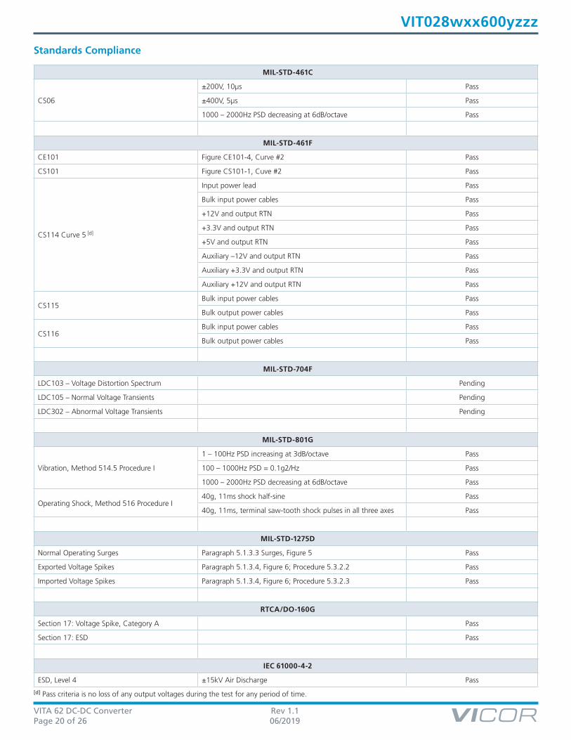
MIL-STD-461C
CS06
±200V, 10µs Pass
±400V, 5µs Pass
1000 – 2000Hz PSD decreasing at 6dB/octave Pass
MIL-STD-461F
CE101 Figure CE101-4, Curve #2 Pass
CS101 Figure CS101-1, Cuve #2 Pass
CS114 Curve 5 [d]
Input power lead Pass
Bulk input power cables Pass
+12V and output RTN Pass
+3.3V and output RTN Pass
+5V and output RTN Pass
Auxiliary –12V and output RTN Pass
Auxiliary +3.3V and output RTN Pass
Auxiliary +12V and output RTN Pass
CS115Bulk input power cables Pass
Bulk output power cables Pass
CS116Bulk input power cables Pass
Bulk output power cables Pass
MIL‐STD‐704F
LDC103 – Voltage Distortion Spectrum Pending
LDC105 – Normal Voltage Transients Pending
LDC302 – Abnormal Voltage Transients Pending
MIL‐STD‐801G
Vibration, Method 514.5 Procedure I
1 – 100Hz PSD increasing at 3dB/octave Pass
100 – 1000Hz PSD = 0.1g2/Hz Pass
1000 – 2000Hz PSD decreasing at 6dB/octave Pass
Operating Shock, Method 516 Procedure I40g, 11ms shock half-sine Pass
40g, 11ms, terminal saw-tooth shock pulses in all three axes Pass
MIL-STD-1275D
Normal Operating Surges Paragraph 5.1.3.3 Surges, Figure 5 Pass
Exported Voltage Spikes Paragraph 5.1.3.4, Figure 6; Procedure 5.3.2.2 Pass
Imported Voltage Spikes Paragraph 5.1.3.4, Figure 6; Procedure 5.3.2.3 Pass
RTCA/DO-160G
Section 17: Voltage Spike, Category A Pass
Section 17: ESD Pass
IEC 61000-4-2
ESD, Level 4 ±15kV Air Discharge Pass
Standards Compliance
[d] Pass criteria is no loss of any output voltages during the test for any period of time.

VITA 62 DC-DC Converter Rev 1.1Page 21 of 26 06/2019
VIT028wxx600yzzz
I2C™ Sensor Commands
Commands are sent by SMBus-compatible packets over the I2C physical interface. The I2C bus will communicate at 100kHz. Pull-up resistors to +3.3V are expected on the system backplane.
Two pins, labeled *GA1 and *GA0 are provided at each power supply slot, where *GA1 and *GA0 are defined to be active (SET) when low. The power supply will respond to I2C address 010 00[GA1][GA0]
The general format is as follows:
�� Command from controller I2C / SMBus master:
Address+R/*W Command Byte Number of Bytes Zero Checksum
�� Response from power supply I2C / SMBus slave:
Command Echo Data Bytes Zero Checksum
Commands Recognized by Power Supply
[e] Most-significant bit of each byte is transmitted first. Most-significant byte of UINT16 and UINT32 transmitted first.
0x21: Sensor Data (Read Only) [e]
Byte Number
Contents Format Scaling
0 0x21 Byte Echo of the command
1 Status Reg ByteSee below, same as used by command 0x55
2, 3 PCBA Temperature ºC INT16 16384 = 100ºC
4, 5 +12V VSENSE UINT16 16384 = 12.0V
6, 7 +3.3V VSENSE UINT16 16384 = 3.3V
8, 9 +5V VSENSE UINT16 16384 = 5.0V
10, 11 +3.3VAUX VSENSE UINT16 16384 = 3.3V
12, 13 +12VAUX VSENSE UINT16 16384 = 12.0V
14, 15 –12VAUX VSENSE UINT1616384 = –12.0V, absolute value
16, 17 +12V IOUT UINT16 16384 = 30A
18, 19 +3.3V IOUT UINT16 16384 = 20A
20, 21 +5V IOUT UINT16 16384 = 40A
22, 23 +3.3VAUX IOUT UINT16 16384 = 4A
24, 25 +12VAUX IOUT UINT16 16384 = 1A
26, 27 –12VAUX IOUT UINT1616384 = –1A, absolute value
28, 29 INT REFERENCE UINT16 16384 = 2.50V
30, 31 Input Voltage UINT16 16384 = 28V
32 – 51 Part Number CHAR[20]no 0 term, padded with 0x20
52 – 55 Serial Number UINT32
Unsigned 32-bit integer; last 9 digits of the serial number of the unit on the label
56, 57 Date Code UINT16
Byte 56: YY - 0x12 is 18 or 2018Byte 57: WW - 0x1A is the 26th Week
58, 59 Hardware Rev CHAR[2] See label information
60, 61 Firmware Rev CHAR[2]
62 Input Current UINT8 255 = 40A
63 Zero Checksum Byte Sum(byte 0:63) = 0
Part number, CHAR Bytes 32 – 51
Year, YY Byte 56
Serial Number, UINT32 Bytes 52 – 55
Mfg. date for Byte 57 WW Jan 01, Day 1 of Week 1
Byte 59 (Char)
Byte 58 (Char)
Figure 31 — Product label information

VITA 62 DC-DC Converter Rev 1.1Page 22 of 26 06/2019
VIT028wxx600yzzz
Commands Recognized by Power Supply (Cont.)
0x44: Firmware Date (Read Only) [f]
• 22 byte response in ASCII form.
Byte Number
Contents Format Typical Value
0 0x44 Byte Echo of the command
1 – 20 Date ASCII[20] ‘NOV 28 14:32:54 2018’
21 Zero Checksum Byte
0x45: Hardware Address (Read Only) [f]
• Uses SMBus Read Byte protocol, section 6.5.5, with or without 0 PEC
Byte Number
Contents Format Typical Value
0 0x45 Byte
1 I2C Address Byte0x23, set by *GA1, *GA0
2 Zero Checksum Byte Sum(byte 0:2) = 0
0x55: Status Command (Read/Write) [f]
• Uses SMBus Wirte Byte/Read Byte protocol, section 6.5.4, 6.5.5, with or without 0 PEC
Byte Number
Contents Format Typical Value
0 0x55 Byte
1 Status Byte Byte 0x18 = All outputs ON
2 Zero Checksum Byte Sum(byte 0:2) = 0
0x90: All Voltages in mV (Read) [f]
Byte Number
Contents Format Scaling
0 0x21 Byte Echo of the command
1, 2 +12V SENSE UINT16 1mV/bit
3, 4 +3.3V SENSE UINT16 1mV/bit
5, 6 +5V SENSE UINT16 1mV/bit
7, 8 +3.3VAUX SENSE UINT16 1mV/bit
9, 10 +12VAUX VSENSE UINT16 1mV/bit
11, 12 –12VAUX VSENSE UINT16 –1mV/bit
13, 14 Input Voltage UINT16 1mV/bit
15 Zero Checksum Byte Sum(byte 0:14) = 0
0x99: Main Outputs – Output and Input Current in mA (Read) [f]
Byte Number
Contents Format Scaling
0 0x99 Byte Echo of the command
1, 2 +12V IOUT UINT16 1mA/bit
3, 4 +3.3V IOUT UINT16 1mA/bit
5, 6 +5V IOUT UINT16 1mA/bit
7, 8 Input Current UINT16 1mA/bit
9 Zero Checksum Byte Sum(byte 0:8) = 0
0x91: Auxiliary Outputs – Output Current in mA (Read) [f]
Byte Number
Contents Format Scaling
0 0x91 Byte Echo of the command
1, 2 +3.3VAUX IOUT UINT16 1mA/bit
3, 4 +12VAUX IOUT UINT16 1mA/bit
5, 6 –12VAUX IOUT UINT16 –1mA/bit
7 Zero Checksum Byte Sum(byte 0:6) = 0
0x92: PCBA Card Edge Temperatures in °C x 10 (Read) [f]
Byte Number
Contents Format Scaling
0 0x92 Byte Echo of the command
1, 23U P0 connector,
P1 side RailINT16
Temperature x 10, eg. –123 = –12.3°C
3, 43U P0 connector,
P6 side RailINT16 Same as above
5 Zero Checksum Byte Sum(byte 0:4) = 0
[f] Most-significant bit of each byte is transmitted first. Most-significant byte of UINT16 and UINT32 transmitted first.

VITA 62 DC-DC Converter Rev 1.1Page 23 of 26 06/2019
VIT028wxx600yzzz
Status Register Bit Map (Byte 1) used in command 0x55
Bit 0 and 1 allow you to monitor what the power supply is reading from the input connector.
*HW En*HW Inh
*SW En
*SW Inh
XFAIL
OT Warning
SW Priority
Read/Write
7 6 5 4 3 2 1 0
0 0 0 0 0 00 0
STATUS REGISTER (Byte 1)(0x55)
Bit Name Condition Default
7 X 0 0
6 FAILIf set to 1 by System Manager,
a fault condition will clear this bit.0
5 OT WarningIf set to 1 by System Manager, an OT fault will clear this bit.
0
4 SW Priority Set to 1 for SW Control 0
3 *SW lnh EN all, 0 EN only 3.3V 0
2 *SW En ALL outputs regardless 0
1 *HW lnh As read by HW BACKPLANE
0 *HW En As read by HW BACKPLANE
VITA 62 DC-DC Converter Rev 1.1Page 24 of 26 06/2019
VIT028wxx600yzzz
Power Architecture
EMI Filter
Reverse VoltageBlocking
VS2+3.3V, 20A
VS3+5.0V, 30A
VS1+12.0V, 40A
VAUX2+3.3V, 6A
VAUX1–12.0V, 1A
VAUX3, +12V, 1A
DC IN
Out
puts
at V
ITA
3U P
0 co
nnec
tor
P6
LP2
P3
C6
B3
A4-D4
Input Power atVITA 3U P0 Connector
P1, P2
Internal Power Configuration
to
to
[g] Card edge temperature sensor proximity.
[g]
[g]

VITA 62 DC-DC Converter Rev 1.1Page 25 of 26 06/2019
VIT028wxx600yzzz
Mechanical Drawing
6.634
3.937
3.197
3.335 .301
THERMAL SEATING PLANE
.950
.257
.393
.495 NOMINAL,WEDGE-LOCKEXPANDS TO.545 MAX. 1 2 3
DIMENSIONS ARE IN INCHES
Connector Components
Item # Description Manufacturer Manufacturer Part Number
1 VITA46 0 DEG Guide Socket TE Connectivity 1-1469492-1
2 VITA62 Connector Plug TE Connectivity 6450849-7
3 VITA46 0 DEG Guide Socket TE Connectivity 1-1469492-1
VITA 62 DC-DC Converter Rev 1.1Page 26 of 26 06/2019
VIT028wxx600yzzz
Revision History
Revision Date Description Page Number(s)
1.0 02/07/19 Initial release n/a
1.1 06/19/19 Changed NC to NO in Tables 1 and 2 17
Contact Us: http://www.vicorpower.com/contact-us
Vicor Corporation25 Frontage Road
Andover, MA, USA 01810Tel: 800-735-6200Fax: 978-475-6715
www.vicorpower.com
emailCustomer Service: [email protected]
Technical Support: [email protected]
©2019 Vicor Corporation. All rights reserved. The Vicor name is a registered trademark of Vicor Corporation.I2C™ is a trademark of NXP semiconductor.
All other trademarks, product names, logos and brands are property of their respective owners.


![current vita [vita]](https://static.documents.pub/doc/80x56/62397044b818b31db60e2000/current-vita-vita.jpg)