Experimental Study of Electron Transport through Nanometer-Scale Metal-Oxide Junctions A Dissertation Presented by Zhongkui Tan to The Graduate School in Partial Fulfillment of the Requirements for the Degree of Doctor of Philosophy in Physics Stony Brook University May 2010
Transcript
Experimental Study of Electron Transport through
Nanometer-Scale Metal-Oxide Junctions
A Dissertation Presented by
Zhongkui Tan
to The Graduate School
in Partial Fulfillment of the Requirements for the Degree of
Doctor of Philosophy
in
Physics
Stony Brook University May 2010
UMI Number: 3408250
All rights reserved
INFORMATION TO ALL USERS The quality of this reproduction is dependent upon the quality of the copy submitted.
In the unlikely event that the author did not send a complete manuscript
and there are missing pages, these will be noted. Also, if material had to be removed, a note will indicate the deletion.
UMI 3408250
Copyright 2010 by ProQuest LLC. All rights reserved. This edition of the work is protected against
unauthorized copying under Title 17, United States Code.
ProQuest LLC 789 East Eisenhower Parkway
P.O. Box 1346 Ann Arbor, MI 48106-1346
ii
Stony Brook University The Graduate School
Zhongkui Tan
We, the dissertation committee for the above candidate for the Doctor of Philosophy degree, hereby recommend acceptance of this dissertation.
Konstantin K. Likharev – Dissertation Advisor Professor, Department of Physics and Astronomy
James E. Lukens - Chairperson of Defense Professor, Department of Physics and Astronomy
Ismail Zahed Professor, Department of Physics and Astronomy
Andreas Mayr - Outside Member Professor, Department of Chemistry
This dissertation is accepted by the Graduate School.
Lawrence Martin
Dean of the Graduate School
iii
Abstract of the Dissertation
Experimental Study of Electron Transport through
Nanometer-Scale Metal-Oxide Junctions by
Zhongkui Tan
Doctor of Philosophy in
Physics
Stony Brook University
2010
This work presents results of an experimental study of electron transport through few
nanometer-scale metal oxide junctions of two types:
First, we have measured transport properties of Nb/Al/Nb junctions fabricated using
thermal oxidation or rf-plasma oxidation at various conditions, with rapid thermal
post-annealing (RTA) to improve junction endurance in electric fields in excess of 10
MV/cm. The results indicate that such junctions may combine high field endurance
(corresponding to at least 1010 write/erase cycles in floating-gate memories) and high
current density (corresponding to 30-ns-scale write/erase time) at high voltages, with very
low conductance (corresponding to retention time scale ~0.1 s) at low voltages. We
discuss the improvements necessary for the use of such junctions in advanced
floating-gate memories.!
Second, we have studied resistive bistability (memory) effects in junctions based on
iv
several metal oxides, with a focus on sample-to-sample reproducibility which is
necessary for the practical use of such junctions, in particular as crosspoint devices of
hybrid CMOS/nanoelectronic circuits. Few-nm-thick layers of NbOx, CuOx and TiOx
have been formed by thermal and plasma oxidation, at various deposition and oxidation
conditions, both with or without rapid thermal post-annealing. The resistive bistability
effect has been observed for all these materials, with particularly high switching
endurance (over 103 switching cycles) obtained for single-layer TiO2 junctions, and the
best reproducibility reached for multi-layer junctions of the same material. Fabrication
optimization has allowed us to improve the OFF/ON resistance ratio to about 103, though
the sample-to-sample reproducibility is so far still lower than that required for large scale
integration.
Key Words: electron transport, metal oxide, crested barrier, rapid thermal annealing,
List of Figures Figure 1.1 Conduction band edge diagrams of various tunnel barriers. ............................. 5!
Figure 1.2 Possible cell structure of NOVORAM/FGRAM. .............................................. 6!
Figure 1.3 Resistive bistability in metal oxides: (a) the dc I"# curve (schematically), and the parameter nomenclature; (b), (c), (d) a cartoon of the apparent bistability mechanism............................................................................................................................................ 11!
Figure 1.4 The general idea of a hybrid CMOS/nanoelectronic circuit. ........................... 12!
Figure 1.5 The nanowire-crossbar add-on (schematically). .............................................. 13!
Figure 2.1 (a) Top view of a 2-inch oxidized silicon wafer. This wafer has been diced into 57 5×5 mm2 chips for further electrical characterization. (b) Top view of one 5×5 mm2 chip containing 18 junctions whose areas has been defined to be 3×3 !m2, 30×30 !m2 and 300×300 !m2. .................................................................................................................... 18!
Figure 2.2 An HR TEM image of a sample from wafer VJCB4. The layer of aluminum oxide is amorphous and about 1 to 2 nm thick. ................................................................ 20!
Figure 2.3: $"# curves for a junction from wafer VJCB4. ............................................... 21!
Figure 2.4 HR TEM images of a sample from wafer VJCB3. .......................................... 23!
Figure 2.5 Typical I"#s from three junctions of wafer VJCB17a. These junctions show great reproducibility and scaling with areas. .................................................................... 27!
Figure 2.6 Temperature dependence of $"# curves from one junction of wafer VJCB17a............................................................................................................................................ 28!
Figure 2.7 $"# curves of junctions of wafer VJCB17b for different durations of annealing at 400!C. ........................................................................................................................... 30!
Figure 2.8 $"# curves of junctions from wafer VJCB17b, with different RTA temperatures, for 30 seconds. ............................................................................................ 31!
Figure 2.9 Illustration of the potential barrier diagram divided by % piece ..................... 34!
Figure 2.10 $-# fitting of a junction from thermally oxidized wafer VJCB4. ................. 35!
Figure 2.11 $-# fitting of a junction from plasma oxidized wafer VJCB3. ..................... 36!
Figure 2.12 $-# fitting of a junction from plasma oxidized wafer VJCB17a with various RTA temperatures from 400 to 550!C for 30 seconds. ..................................................... 37!
vii
Figure 2.13 Aluminum oxide tunnel barrier height and thickness obtained from Matlab simulation for junctions of wafer VJCB17a within RTA temperatures ranging from 400 to 550!C for 30 seconds. ....................................................................................................... 38!
Figure 2.14 (a) Aluminum tunnel barrier height and (b) barrier thickness, obtained from Matlab simulation for junctions of wafer VJCB17c, 22, 23 and 24 with O2 pressure ranging from 5 to 60 mTorr during plasma oxidation. ...................................................... 39!
Figure 2.15 Typical $"# curves from junctions of double layer wafers. .......................... 43!
Figure 2.16 Breakdown Voltage #BD at room temperature and liquid helium temperature, for junctions fabricated at various rf plasma power from 10 to 250 W, as grown or after RTA at 400!C for 30 seconds. ........................................................................................... 45!
Figure 2.17 Schematic illustration of voltage pulses used in endurance test.. .................. 46!
Figure 2.18 Frequency dependence of &BD for same amplitude of voltage pulses, in the range of 100 Hz to 10 MHz, as well as dc applied voltages. ............................................ 47!
Figure 2.19 &BD dependence of applied voltages. ............................................................ 48!
Figure 2.20 Voltage dependence of &BD for junctions of several wafers. ......................... 49!
Figure 2.21 % vs " for junctions of wafer VJCB17a, with different RTA conditions. ...... 50!
Figure 2.22 Linear fit of ln(%) vs ln(") for junctions of wafer VJCB17c, after RTA at 400ºC for 30 seconds. ....................................................................................................... 51!
Figure 2.23 Field endurance parameter %/"2 and retention time scale "R as functions of RTA conditions.. ................................................................................................................ 52!
Figure 2.24 Field endurance parameter %/"2 as a function of aluminum oxidation conditions. Wafers CB22, CB17C, CB23 and CB24 were fabricated just as CB17a, but at different O2 pressures. ....................................................................................................... 53!
Figure 3.1 Diagram of our evaporation system (called “Pb system”) with major components listed. ............................................................................................................. 60!
Figure 3.2 Diagram of one of our sputtering systems (called “IBM system”) with major components listed. ............................................................................................................. 61!
Figure 3.3 An ADF-STEM image of a sample from wafer VJTiOx8. .............................. 63!
Figure 3.4 Diagram of the reactive ion etch (RIE) system with major components listed............................................................................................................................................ 64!
Figure 3.5 Schematic illustration of fabrication flow of one TiOx wafer... ....................... 66!
viii
Figure 3.6 Typical dc I"# curve of a junction from wafer VJNbOx3. .............................. 71!
Figure 3.7 Typical dc I"# curve of a junction from wafer VJNbOx3 after RTA. ............. 71!
Figure 3.8 Effect of temperature of a 30-second RTA on the OFF/ON resistance ratio and the yield of good devices from wafer VJNbOx3. ............................................................. 72!
Figure 3.9 Multi-level switching of a junction from wafer VJNbOx2 after RTA............. 73!
Figure 3.10 Schottky I-# curves of a junction from wafer VJNbOx4. ............................. 74!
Figure 3.11 Resistance distributions of junctions from wafer VJCuOx3. ........................ 75!
Figure 3.12 Typical dc I"# curve of a junction from wafer VJCuOx7. ............................ 77!
Figure 3.13 Typical dc I"# curve of a junction from wafer VJCuOx7 after RTA. ............ 77!
Figure 3.14 Effect of temperature of a 30-second RTA on the OFF/ON resistance ratio and the yield of good devices from wafer VJCuOx7. ....................................................... 78!
Figure 3.15 One dc I"# curve of a junction from wafer VJCuOx7 after RTA, with ROFF/RON=2.5..................................................................................................................... 78!
Figure 3.16 One dc I"# curve of a junction from wafer VJCuOx15 after RTA, with ROFF/RON=30...................................................................................................................... 79!
Figure 3.17 Temperature dependence of I-# hysteresis loops of a junction from wafer VJTiOx4. ........................................................................................................................... 82!
Figure 3.18 Time dependence of current at 1 V at room temperature. Two junctions with different areas are both from wafer VJTiOx4. .................................................................. 82!
Figure 3.19 Typical dc I"# curve of a junction from wafer VJTiOx2 after RTA. ............. 83!
Figure 3.20 Effect of temperature of a 30-second RTA on the OFF/ON resistance ratio and the yield of good devices from wafer VJTiOx2. ........................................................ 84!
Figure 3.21!Schematic illustration of voltage pulses used in endurance test.. .................. 85!
Figure 3.22 Results of the “endurance test” (repeated ON/OFF cycling) of a junction from wafer VJTiOx2 after RTA. ...................................................................................... 85!
Figure 3.23 (a) EELS spectrum location references in an ADF-STEM image. Scale bar is in nanometers. (b) Typical electron energy loss peaks of titanium and oxygen in an EELS spectrum. ........................................................................................................................... 88!
Figure 3.24 (a) EELS signal profile of titanium, (b) EELS signal profile of oxygen and (c) the relative concerntration of titanium and oxygen of a device from wafer VJTiOx8. .... 89!
ix
Figure 3.25 EELS signal profile of platinum of a device from wafer VJTiOx8. .............. 90!
Figure 3.26 An ADF-STEM image of a junction from wafer VJTiOx17 (7 cycles). ....... 90!
Figure 3.27 EELS signal profiles of (a) platinum, (b) oxygen and (c) titanium of a device from wafer VJTiOx8. Spectrum location references are given in (d). .............................. 91!
Figure 3.28 DC I"# curves of three different devices from wafer VJTiOx8 before the RTA................................................................................................................................... 93!
Figure 3.29 Statistics of the switching thresholds #t and #*t for “as grown” devices (i.e. before the RTA) from wafer VJTiOx8. ............................................................................. 94!
Figure 3.30 Typical dc I"# curve of a junction from wafer VJTiOx8 after the RTA. ....... 95!
Figure 3.31 Effect of temperature of a 30-second RTA on the OFF/ON resistance ratio and the yield of good devices from that wafer. ................................................................. 95!
Figure 3.32 Typical dc I"# curve of a junction from wafer VJTiOx17. (7 cycles) Positive current is set in log scale to be visible in the plot. ............................................................ 96!
Figure 3.33 Diagram of setup for short voltage pulses measurements. ............................ 99!
Figure 3.34 One dc I"# curve of a junction from wafer VJa-SiAg1. .............................. 101!
Figure 3.35 Layout of one CMOS chip. ......................................................................... 102!
Figure 3.36 Actual microphotographs of CMOS chip surface. ...................................... 103!
Figure 3.37 Integration steps for demonstration of CMOS/nanoelectronic circuits. ...... 105!
x
List of Tables Table 1.1 List of values of dielectric constants, band gaps and conduction band offset for several dielectric materials. ................................................................................................. 8!
Table 2.1 Fabrication parameters of thermally oxidized wafer. ........................................ 19!
Table 3.1 Some recently reported results for latching switches based on metal oxides, sulphides, silicon oxide, and amorphous silicon. .............................................................. 56!
Table 3.2 Melting point and coefficient of thermal expansion. ........................................ 67!
Table 3.3 Parameters and properties of NbOx samples. ................................................... 69!
Table 3.4 Parameters and properties of CuOx samples. .................................................... 76!
Table 3.5 Parameters and properties of single layer TiOx samples. .................................. 80!
Table 3.6 Parameters and properties of multi-layer TiOx samples. ................................... 86!
Acknowledgement
First and foremost, I would like to express my gratitude to my advisor, Professor
Konstantin K. Likharev. His extensive guidance and support were always with me in last
five years toward my Ph. D. He is a role model rather than an advisor, for his
encouragement and helps in every detail of scientific behavior and life style.
My graduate studies at Stony Brook have been greatly enriched by the wonderful
condensed matter physics group. I am deeply indebted to Professor James E. Lukens for
the kind permission to use his lab’s fabrication facilities and numerous discussions, and to
Dr. Vijay Patel, Dr. Yuri Polyakov, Dr. Wei Chen for years of experimental support
throughout my entire research projects. I am very grateful for technical support of Dr.
Dong Su and Dr. Yimei Zhu in TEM training and imaging, and Dr. Andreas Mayr in
molecule and polymer synthesis. I also thank Dr. Xueqing Liu, Dr. Shawn Pottorf,
Shi-sheng Chang and Esteban Monge for their technical assistance.
Last and most, I would like to express my gratitude toward my wife, Xiaolan Ba. Her
enormous love and unlimited support in years have delighted my life and kept me
focused on my interests. This dissertation is as much hers as mine.
1
Chapter 1
Introduction
Semiconductor integrated circuit technology (whose most wide-spread version is
usually dubbed CMOS) has been perhaps the most significant technological advance of
our civilization during the past half century. It was driven by the demand for higher
computing power and larger data storage capacity. Fundamentally, the integrated circuit
(IC) industry has employed the “top-down” approach, in which electron devices are
fabricated by such processes as silicon doping and thin-film deposition, and patterned
using optical lithography. The key advantage of this approach is that the components are
built in place, so that no part assembly is needed. In the last few decades, the number of
individual transistors that can be placed on a single integrated circuit chip has been
doubled every 18 months or so (the “Moore’s Law”, first noted by Gordon E. Moore of
Intel). This exponential progress has enabled all the information technology revolution
including the Internet, and wide proliferation of inexpensive, high-performance silicon
chips into every pore of our everyday life.
2
However, it is generally accepted now that this progress will turn into a crawl at
some time during the next decade. [1] Among several reasons of this anticipated crisis,
(i.e. device performance degradation and power dissipation growth [2]), probably the
most fundamental one is that the workhorse active device of the integrated circuits, the
silicon field-effect transistor (MOSFET), requires an accurate definition of several
dimensions including the length and width of its conducting channel. As these devices are
scaled down, arising quantum mechanical effects require the definition to be more and
more precise [3-7], which in turn requires more and more complex and expensive
patterning tools. At some point, the scaling will start bringing diminishing returns, and
the IC industry will stall (“mature”). This would have innumerable negative
consequences for the industry, technology, and everyday life.
It is frequently argued [8] that the “Moore’s Law” demise may be avoided by
switching to the “bottom-up” approach, in which active device components of the
integrated circuits are chemically synthesized and thus have the nature-given,
fundamentally similar size and shape. This approach has indeed resulted in the successful
experimental demonstration of several molecular versions of active electronic devices,
for example, single electron transistors [9-16]. However, to our best knowledge, there
have been virtually no practicable ideas how much nanometer-scale multi-terminal
devices could be effectively integrated into a very large scale integrated (VLSI) circuit,
because this requires nanometer-accurate placement of the components. This is why,
while the silicon-based technology may still serve as a mainstream platform for most IC
3
technologies in the next few decades, alternative technologies, including new materials,
devices, circuits and system-level architectures are clearly needed [17]. This Ph. D. thesis
describes my work in the following two directions of this general field, where such
advances look especially promising.
A. Advanced Memories.
Memory is one of the most important parts of any contemporary electronics systems,
including all modern computers, mobile phones, digital cameras, portable digital
audio/video players, etc. [18, 19]. It can store digital data for a certain period of time,
either requiring external power supply or not. Most types of random access memory
(RAM), including dynamic random access memory (DRAM) and static random access
memory (SRAM), are “volatile”, i.e. require power supply for data storage. On the
can retain the stored information without power supply for years.
Among all kinds of nonvolatile memories, NAND flash memory is the fastest
growing segment of the memory market because of its high density. However, such
memory has much lower program and erase speed (in the !s and ms ranges, respectively),
compared to that of CMOS logic (whose clock cycles are in sub-ns range). It would be a
great achievement to develop a nonvolatile memory with high operation speed
(comparable to volatile RAMs), while still keeping the standard 10-year data retention
ability.
The operation of current flash memory cells is based on Fowler-Nordheim tunneling
4
through an 8-nm-scale-thick SiO2 layer (Figure 1.1a) separating a virtually isolated
electrode called floating gate, located between the control gate and the MOSFET channel,
from the latter electrode. Any electrons placed on the floating gate are trapped there and,
at low voltages applied to the control gate, would not discharge for many years. High
(~15 V) voltage applied to the control gate induces a very high (~10mV/cm) electric field
in the SiO2 layer. This field tilts the potential barrier as shown in Figure 1.1, and thus
suppresses the potential barrier for electron tunneling to/from the floating gate. As a
result, the quantum-mechanical transparency of the tunnel barrier increases by more than
10 orders of magnitude, and the floating gate recharges. However, as already mentioned
above, this huge difference is still insufficient to provide the difference between the
retention and write/erase time necessary to combine memory’s nonvolatility and
randon-access operation.
5
Figure 1.1 Conduction band edge diagrams of various tunnel barriers: (a) a typical uniform barrier; (b) idealized crested symmetric barrier; (c) idealized asymmetric barrier, (d) crested, symmetric layered barrier, and (e) asymmetric layered barrier. Dashed lines in panels a) and b) show the barrier tilting caused by applied voltage #.
Other panels of Figure 1.1 show the conduction band edge diagrams of various
non-uniform (“engineered”) tunnel barriers [20]. According to calculations [20-25], the
rate of quantum-mechanical tunneling of electrons through such barriers, in particular
those with “crested” potential profile peaking in the middle, may be much more sensitive
to the voltage applied to the barrier [26]. This sensitivity may enable fast and scalable
nonvolatile random-access memories (“NOVORAM”) [20, 22] with a simple cell
structure (Figure 1.2), and a matrix architecture similar to that of NOR flash – see, e.g.,
6
Reference 27. The main difference of the NOVORAM cell from the flash is that the
tunneling layer, responsible for write/erase operations, is moved to the back of the
floating gate. In this geometry, the floating gate may be metallic, and its thickness
reduced to a few nanometers, thus dramatically reducing the electrostatic crosstalk of the
adjacent cells, and making the cells scalable to at least 10 nm.
Figure 1.2 Possible cell structure of NOVORAM/FGRAM.
There are several factors that need to be taken into account when selecting the
appropriate materials to demonstrate a crested barrier. The key parameters to characterize
a tunnel barrier include the barrier height, dielectric constant, thickness and effective
mass of charge carriers in each dielectric layer. The barrier height U relates to work
function , of the metal electrode and the electron affinity # of the dielectric by
U = , – #. (, is defined as the difference between the vacuum level and the Fermi
7
energy of the metal electrode and # is the difference between the vacuum level and the
conduction band edge of the dielectric.) U is the most important parameter that
determines the barrier performance. Ideally, the barrier height in the middle of the
“crested” barrier should be 1 to 2 eV higher than that of its sides (Figure 1.1b). Simple
quantum-mechanical (say, WKB) calculations show that the fast suppression of such
barrier by the applied voltage may provide the fast change of the tunnel current.
The dielectric constant k will also affect the performance of the barrier. Under
applied voltage bias, the electric field in the barrier automatically redistributes so that it is
inversely proportional to the dielectric constant, changing the potential barrier profile. In
addition, the effective mass me and physical thickness d of each layer will affect the
performance of crested barriers as a whole (me1m0)1/2d. Table 1.1 lists the reported
(relative) dielectric constants k, band gaps and conduction band offset of interesting
dielectric materials.
8
Table 1.1 List of values of dielectric constants, band gaps and conduction band offset for several dielectric materials [28-35].
Material k #G (eV) U – Si (eV) U – Au (eV) U – Nb (eV) me
SiO2 3.9 9 3.5 4.0 3.2 0.5
Al2O3 9 9 2.8 3.4 2.6 0.2-0.5
Si3N4 7.8 5.3 2.4 2.9 2.1 0.4
HfO2 18 6 1.5 2.1 1.3 0.2
ZrSiOx 12.6 6 1.5 2.1 1.3 0.3
ZrO2 25 5 1.4 2.0 1.2 0.3
In summary, to build a crested barrier with steep I$# curves, we need to consider the
electron affinity and dielectric constant of the dielectrics, the work function of the metal
electrode and the effective thickness of each layer. Just a few known CMOS compatible
materials [36] may combine the barrier height sufficient for thermionic current
suppression at room temperature (above 1.5 eV), with the necessary high breakdown field
(above 10 MV/cm) and negligible trap-assisted tunneling. The list of such candidate
materials is essentially limited to:
(1) silicon dioxide;
(2) low-trap density silicon nitride [37, 38]; and
(3) aluminum oxide grown by a variety of methods including thermal [39] and
plasma [40] oxidation.
9
Published experimental work has shown that layered barriers made of several material
combinations, including SiO2/ZrO2 [41], Si3N4/SiO2 [42-45], Si3N4/Al2O3 [46],
HfO2/Al2O3 [46], HfON/Si3N4 [47], SiO2/HfO2 [48, 49], and Al2O3/HfO2/SiO2 [50], can
indeed improve the sensitivity of tunneling transparency to voltage in comparison with
the traditional uniform (e.g., SiO2) barriers. Unfortunately, the transparency change scales
demonstrated so far are still insufficient for the implementation of the NOVORAM
concept. In particular, attempts by our group to combine two different (thermally-grown
and plasma-grown) species of aluminum oxide [51] to form high-performance layered
barriers have not been working so far, apparently due to the uncontrollable interfacial
chemistry and/or charge trapping. However, in the process of this work we have found
that uniform plasma-grown AlOx, a material with high dielectric constant, large band gap
and large barrier height, may approach the requirements of the so-called Floating-Gate
Random-Access Memories (FGRAM) [52, 53]. The cell and matrix structure of FGRAM
is similar to those of NOVORAM (Figure 1.2), and essentially the only difference is the
necessity to refresh the FGRAM periodically, due to the relatively short retention time,
just like this is being done in the usual dynamic random-access memories (DRAM). The
goal of this work was to study the high-field endurance of AlOx-based tunnel junctions,
which is necessary for NOVORAM and FGRAM applications, within a much broader
range of the aluminum oxidation and rapid thermal post-annealing (RTA) conditions than
it had been done in our group’s initial study [51].
10
In Chapter 2, I describe the results of our study of electron tunneling through
junctions based on thin aluminum oxide layers, especially post-processed using rapid
thermal annealing (RTA), with a focus on the bias voltage effects, including high field
endurance.
B. Hybid CMOS/Nanoelectronic Circuits.
During the past few decades, numerous research groups have run into the
experimental fact that thin layers of quite a few materials, including several organic
compounds (sometimes with embedded metallic clusters), chalcogenides, metal oxides,
amorphous silicon, and self-assembled molecular monolayers exhibit the “resistive
memory effect” (resistive bistability).
The device with resistive bistability has an I"# curve with two branches
corresponding to its two possible internal states, i.e. low-resistive (OFF) state and
high-resistive (ON) state (Figure 1.3a). It may be switched between its ON and OFF
states by applying voltages exceeding the corresponding threshold values #t and #*t .
These studies have led to a virtual consensus that the resistive bistability, at least in
metal-oxide and amorphous-silicon junctions, is due to the reversible formation and
dissolution of one or few highly conducting spots (sometimes called “filaments”), due to
field-induced drift of ions (depending on the particular material, either anions or cations)
through the amorphous matrix of the layer – see Figure 1.3b-d [55, 56, 64].
11
Figure 1.3 Resistive bistability in metal oxides: (a) the dc I"# curve (schematically), and the parameter nomenclature; (b), (c), (d) a cartoon of the apparent bistability mechanism.
Such simple two-terminal devices can serve as a memory cell storing one bit of
information in its internal state, but cannot amplify signals as a transistor, and hence
cannot be the sole basis for useful integrated circuits. However, a layer of very small
devices of this kind, being added to a semiconductor-transistor circuit with much cruder
features (Figures 1.4 and 1.5), can strongly enhance its functionality, without an
unacceptable increase of the fabrication costs. This idea of hybrid CMOS/nanoelectronic
circuits (in particular their variety called CMOL, initially standing for CMOs/MOLecular
12
circuits) [4], [54] has a fast progress during the past couple years.
Figure 1.4 The general idea of a hybrid CMOS/nanoelectronic circuit.
13
Figure 1.5 The nanowire-crossbar add-on (schematically).
A nanowire crossbar (Figure 1.5) contains simple, similar nanodevices (with resistive
bistability, in our case) at each crosspoint. The crosspoint device would include a
single-bit memory cell whose contents could control the connection of two nearby
nanowires. In this way, the distributed crossbar memory may control the configuration of
the system. Due to the sharp switching thresholds of these devices with resistive
bistability (Figure 1.3a), each of them may be uniquely addressed, e.g., turned ON or
OFF, applying appropriate voltages (close to ±2/3 #t) to the two corresponding nanowires.
This produces the net voltage higher than #t across the selected device, and switches it,
without changing the states of other, “semi-selected” devices contacting just one of the
nanowires.
In several recent studies, prospects of CMOL circuit applications in which the
following systems have been explored [1].
14
1.! CMOL memories, which are just a hybrid-circuit extension of resistive memories,
with each bit stored in the internal state of a certain crosspoint device, but
peripheral functions embodied in the CMOS subsystem, may enable eventually
terabit-scale integration.
2.! CMOL reconfigurable (FPGA-like) logic circuits may provide a density
advantage of about 2 orders of magnitude over purely CMOS circuits of the same
functionality and power density, at comparable speed.
3.! Though custom CMOL VLSI circuits have not been explored to any detail yet,
there are preliminary indications that these circuits will have a lower advantage in
density, but substantially increased speed (again, at the same power).
4.! Mixed-signal neuromorphic CMOL networks (“CrossNet”) may provide
extremely high performance for certain advanced information processing tasks
such as pattern classification (including ultrafast feature recognition), and more
intelligent tasks, in particular those requiring in-situ training and global
reinforcement learning.
Based on these studies, one can summarize the requirements for resistive memory
cells as follows [57]:
1.! WRITE voltages #wr should be in the range of a few hundred mV to few V. The
desired duration of the WRITE voltage pulses "wr is below 100 ns.
2.! READ voltages #rd need to be significantly smaller than #wr, but because of
constraints by circuit design, #rd cannot be less than approximately one tenth of
15
#wr. In the ON state, the minimum READ current Ird should not be less than
approximately 1 !A to allow for a fast detection of the state by reasonably small
sense amplifiers. The READ time trd must be in the order of "wr or preferably
shorter.
3.! A resistance ratio ROFF/RON >10 is required to allow for small and highly efficient
sense amplifiers.
4.! The resistive memory should provide at least the same number of WRITE cycles
as those of contemporary flash memories, which is 103 to 107, depending on the
particular application.
5.! A data retention time "ret in excess of 10 years is required for universal
nonvolatile memories. This retention time must be kept at thermal stress up to
85ºC and small electrical stress such as a constant stream of #rd pulses.
Chapter 3 describes our work on the fabrication and electrical characterization of
junctions with resistive bistability, based on metal oxide thin layers of NbOx, CuOx, and
TiOx. In contrast to earlier work, we have emphasized the sample-to-sample
reproducibility, as well as key parameters of resistance bistability, such as threshold
voltages, ON/OFF conductance ratio and cycling endurance. High-resolution TEM
studies have been carried out to reveal the microscopic structures of our junctions.
16
Chapter 2 Aluminum oxide tunnel barriers with high field endurance
2.1 Fabrication and experiment procedures Tri-layer structures, which were the basis of our samples, have been grown on 2-inch
silicon wafers (p-doped to resistivity % = 1-10 "·cm), covered by 500 nm of thermally
grown SiO2. Such a wafer has been loaded into a vacuum system, with a base pressure at
2-3×10⁻⁷ Torr, which had been developed earlier for fabrication of standard Nb-trylayer
junctions. The first layer of a 150-nm-thick niobium base film has been deposited by
dc-magnetron sputtering at a rate of 1.6 nm/s. Without a vacuum break, a few-nm
(usually 3 to 10 nm) aluminum thin film has been deposited by the same method at a
lower rate of 0.5 nm/s. Under these conditions, aluminum thin films wet the niobium
surface [58], forming a smooth uniform coating.
Following the aluminum deposition, it has been oxidized by either thermal oxidation
or plasma oxidation. For thermal oxidation, a fixed amount of ultra-high-purity oxygen
has been let into the vacuum chamber for a certain time (at room temperature). On the
other hand, during plasma oxidation, we have used the same gas (static) as well as an
oxygen flow (dynamic) at a fixed flow rate controlled by a mass flow meter, at oxygen
pressure ranging from 5 to 75 mTorr. In this case, a 13.56 MHz rf power source has been
17
connected, via a tuned resonant circuit, to a dc-insulated copper plate on which the
substrate had been mounted. This has resulted in a 10 to 250 W rf plasma discharge and
wafer dc self-biasing to approximately -80 V relative to the ground (See Tables 2.1 and
2.2 for detailed fabrication parameters). This wafer has always been kept at room
temperature by its thermal anchoring to the water-cooled copper plate.
After the oxidation, the chamber has been pumped down to the base pressure shown
above, and a niobium counter-electrode (100 nm) has been deposited by the same method
as the base electrode.
After the tri-layer deposition, the sample has been patterned (with areas A ranging
from 3×3 to 300×300 !m2, see Figure 2.1b for top view of a chip configuration) using
deep ultra-violet (DUV) lithography with photo resist (PMMA) and reactive ion etching
(RIE) in SF6 plasma. Here, the same photomask was first used for the counter electrode
definition using RIE, and later for a self-aligned lift-off of a dc sputtered 150-nm SiO2 as
insulation layer. This lift-off has opened contacts of junction counter-electrodes with
another thicker niobium layer as wiring layer.
18
(a) Top view of 2-inch wafer (b) Top view of 5 × 5 mm2 chip
Figure 2.1 (a) Top view of a 2-inch oxidized silicon wafer. This wafer has been diced into 57 5×5 mm2 chips for further electrical characterization. (b) Top view of one 5×5 mm2 chip containing 18 junctions whose areas has been defined to be 3×3 !m2, 30×30 !m2 and 300×300 !m2.
After initial characterization, several samples from each wafer have been subjected to
rapid thermal post-annealing (RTA) in an argon flow for 10 to 180 seconds at a
temperature between 300 and 550!C.
Two-terminal DC current-voltage (I"#) measurements of both “as grown” and
annealed junctions have been carried out at both room (~300 K) and liquid helium (LH,
4.2 K) temperatures, by a special low-noise, high-sensitive source meter (Keithley 6430).
Voltage sweeps with different amplitudes and steps have been used to characterize
transport properties until the oxide hard breakdown. In order to present low-voltage data
19
in more obvious form, we have frequently plotted the dynamic (differential) junction
conductance $ " dI/d# (in the log scale) as a function of # (in the linear scale).
2.2 Thermally oxidized (TO) wafer
Table 2.1 Fabrication parameters of thermally oxidized wafer.
Wafers Base Electrode Al O2 Pressure Time RTA
VJCB4 Nb, 50 nm 3 nm 100 Torr 50 min 400 to 500!C, 30 s
Table 2.1 has lists parameters of our only thermally oxidized wafer, VJCB4.
Specifically, a 3-nm aluminum layer was deposited on top of the Nb base electrode for a
thorough oxidation in pure oxygen. Some chips have been subject to RTA at 400 to
500!C for 30 s to improve transport properties.
20
Figure 2.2 An HR TEM image of a sample from wafer VJCB4. The layer of aluminum oxide is amorphous and about 1 to 2 nm thick.
High resolution transmission electron microscopy (HR TEM, see Figure 2.2) study has
shown that the aluminum oxide layer was amorphous, with a thickness of 1 to 2 nm.
Electrical characterization at room and LH temperatures has shown that the deep
refrigeration shifts I"# curves by a small fraction (<5%), a good indication of direct
quantum-mechanical tunneling – see Figure 2.3. However, the breakdown voltages were
low (~1 V), which are not suitable for FGRAM applications. Further variation of RTA
parameters did not improve the breakdown voltages.
"#$%!
"#!
&'$(!
)*!
+!,-!
21
"#$% "%$& %$% %$& #$% #$&
'(#%)
*(#%)+(#%))(#%)#%,
-./0.1!23-.04!53463785073
!
!963:.;.:!<=>10:58>:3!?9@4
' A
B=-58C3!?BA
BDE.F(*
<2.6!%%G!D0>!'
7==4!53463785073
Figure 2.3: $"# curves for a junction from wafer VJCB4.
We have observed the increase of #BD for virtually all junctions as well as the decrease
of $(0) after RTA at temperatures from 300!C to 500!C. Typical I"# curves of annealed
samples were shown in Figures 2.7 and 2.8 for different annealing temperatures and
duration, from junctions of wafer VJCB17b.
30
Figure 2.7 $"# curves of junctions of wafer VJCB17b for different durations of annealing at 400!C.
"* "H "' "# % # ' H *#%"#
#%%
#%#
#%'
#%H
#%*
#%&
#%+
#%I
!
!963:.;.:!<=>10:58>:3!!!!?9@4
' A
B=-58C3!"!!?B=-5LA
!8L"C7=N>!*%%=<!#%L!*%%=<!H%L!*%%=<!#)%L
31
Figure 2.8 $"# curves of junctions from wafer VJCB17b, with different RTA temperatures, for 30 seconds.
As Figures 2.7 and 2.8 show, the junctions tend to have higher #BD and lower $(0) at
higher annealing temperature and longer annealing time. We have also observed the
post-annealing results in a substantial improvement of the junction endurance in high
electric fields. In particular it increases the static breakdown field well above 10 MV/cm
at room temperature (and above 15 MV/cm at 4.2K), i.e. substantially beyond that of the
best SiO2 layers we are aware of. The floating gate recharging time scale is defined as % "
C#/I(#), where C is the junction capacitance, # and I(#) are applied voltage and
"* "H "' "# % # ' H *#%"H#%"'#%"##%%#%##%'#%H#%*#%&#%+#%I
%!&!%$#L
B=-58C3!"!?B=-5LA
963:.;.:!<=>10:58>:3!!!?9@4
' A
!
!
!
!
!8L!C7=N>!*%%=<!H%L!*&%=<!H%L!&%%=<!H%L!&&%=<!H%L
%!&!H%>L
32
tunneling current of the junction, respectively. Because of this high field endurance of our
AlOx junctions, the applied voltage may change the time scale % by more than 9 orders
of magnitude. i.e. the junction with RTA at 500!C for 30 seconds shown in Figure 2.8,
has the write (program) time of % # 10 ns at V # 3.5V, and the retention time % # 10 s at V
= 0 V.
2.4 Simulation and fitting results Based on the free electron approximation [59], direct coherent tunneling current
through typical metal-insulator-metal devices may be calculated by jointly solving the
Schrodinger equation and Poisson equations. Assuming that the energy of the tunnel
electron and the transverse component of the momentum are both conserved, the
tunneling current density is given by:
! " #$%&'()* + ,-. + ,-/01-.23
434 -/56789-.2-/: ; 7<9-.2-/:= (2.1)
where 0 is the transmission coefficient; -., -/ are the local energy and the transverse
energy of a tunneling electron; me is the effective mass of the transverse electron and fL,
fR are the equilibrium Fermi-Dirac distribution functions in the left and right electrodes.
We can use a 1D model to describe the barrier profile. The tunneling current density
includes the carrier transport in both directions between two metal contacts. In the case of
T = 0, the Fermi energy function of the metal is written as:
7>9-.2-/: " ?-@>A2 B7A-. AC -@>ADAAA2 B7A-. AE -@> A2 B " F2 GA (2.2)
33
where EfL and EfR are Fermi energies of left and right metal layers, respectively. Using
this function, the current density J may be simplified as:
! " !8H< ; !<H8 " #$%&'()* AIJK + 01-.5,-.LMNO#P
4 Q + 01-.51-@8;-.5,-.LMNLMNO#P R (2.3)
For the case of T > 0, we assume that the electrons are distributed according to
equilibrium Fermi-Dirac distribution in both electrodes, determined by the bulk Fermi
levels on the respective sides of the barrier:
781-.2 -/5 " ST1S Q UVW XLYZL[OLMN\]^_ ` (2.4)
7<1-.2 -/5 " ST1S Q UVW XLYZL[OLMNZ#P\]^_ (2.5)
After integration over the transverse energy ,-/ for the second integral in equation
(2.1), we obtain:
a " #$%&'()* bcd + 01-.5efA1 gZ#1hMNihY5Tj]k
gZ#1hMNihYi%l5Tj]k34 5,-. (2.6)
This result is called the Tsu-Esaki formula, and the logarithmic term is named the
“supply function”.
The key parameter in the tunneling current is the transmission coefficient 0. To
calculate 0, we have used the transfer matrix formalism method to numerically solve the
Schrodinger equation and Poisson equation. [60] By breaking the potential barrier into N
sequential pieces (Figure 2.9), the transmission coefficient can be calculated to arbitrary
precision (in the independent-electron picture). For each slice i, the Schrodinger equation
can be solved analytically, its transmission matrix found as:
34
g& mJn\op DD JOn\opq m
S Q b>r>ZgTb>Zgr> S ; b>r>ZgTb>Zgr>S ; b>r>ZgTb>Zgr> S Q b>r>ZgTb>Zgr>
q (2.7)
where b " str1- ; u5 for slice i. Then the total transfer matrix may be found as a
product of such matrices calculated for each slice, and the transmission coefficient 0
calculated as:
0 " $N\v$v\N
wxyz{xyw&" $N\v
$v\N|}~1S2S5|& (2.8)
where mL and mR are the effective electron masses in the junction electrodes, )b82< is x
component of the momentum of electron in left or right electrodes, |�4|2 is the amplitude
of incoming wave function in the left electrode, |�~Zg|2 is the amplitude of outgoing
wave function in the right electrode. After the transmission coefficient 0 has been
obtained for each value of Ex, current density may be calculated from Equation (2.6) by
numerical integration over all substantial energies (typically, within a few hundred meV
below the highest Fermi surface).
Figure 2.9 Illustration of the potential barrier diagram divided by N piece
35
Figure 2.10 and Figure 2.11 show quantitative simulation results by Matlab, using hot
electron model to obtain the barrier height and thickness. The simplest junction geometry
is a tilted tunnel barrier between two niobium electrodes.
%$%%#
%$%#
"#$& "# "%$& % %$& # #$&
1?#@A&'B0C53-6.230D0E.6F0/.6
<O*PQ#%G!R)!*$'M
'8S#$,3BG!('S%$&3BG!1S#$I'>4
B=-58C3!?BA Figure 2.10 $-# fitting of a junction from thermally oxidized wafer VJCB4.
Figure 2.10 shows the results of such fitting for one of the thermally oxidized
junctions from wafer VJCB4. Here the average barrier height of thermally oxidized
aluminum oxide is &=1.9 eV, with $&=0.5 eV, with the effective electron mass me=0.32m0
and the barrier thickness is d=1.72 nm. This thickness is close to that obtained by the
direct observation of the oxide layer in the HR TEM image of a similar junction (see
Figure 2.2).
36
"* "H "' "# % # ' H *
#%"'
#%%
#%'
#%*
#%+
#%)
B!?BA
T?J@B@4' A
Figure 2.11 $-# fitting of a junction from plasma oxidized wafer VJCB3.
In Figure 2.11, the average barrier height is &=2.5 eV, with $&=1.25 eV, with electron
effective mass me=0.5m0 and the barrier thickness is d=2.8 nm, with the last number close
to the direct observation of the oxide layer in the HR TEM image of a similar junction in
Figure 2.4.
This simulation method has also been applied to the post annealed junctions, in order
to get an idea of the physical change of aluminum oxide tunnel barriers as a result of the
RTA. Figure 2.12 shows simulation results of junctions from wafer VJCB17a at various
37
RTA temperatures for 30 seconds. Figures 2.13 and 2.14 summarize the fitting
parameters.
#%"H
#%"#
#%#
#%H
#%&
#%I
"* "H "' "# % # ' H *
<O#I!8L!C7=N>
<O#I!UEJ!*%%=<!H%L
<O#I!UEJ!*&%=<!H%L
<O#I!UEJ!&%%=<!H%L
<O#I!UEJ!&&%=<!H%L
B=-58C3?BA Figure 2.12 $-# fitting of a junction from plasma oxidized wafer VJCB17a with various RTA temperatures from 400 to 550!C for 30 seconds.
38
#$&
'
'$&
H
'
'$&
H
H$&
*
*%% *&% &%% &&%
O877.37 E2.:V>3LL
J>>38-.>C!E3463785073?=<AUE
Figure 2.13 Aluminum oxide tunnel barrier height and thickness obtained from Matlab simulation for junctions of wafer VJCB17a within RTA temperatures ranging from 400 to 550!C for 30 seconds.
39
% #% '% H% *% &% +%#$,%
#$,&
'$%%
'$%&
'$#%
'$#&
'$'%
!
!
<O'*
<O'H
<O#I<
O877.37!W3.C25!?#"A
F'!X73LL073!?$%&''A
!8L!C7=N>!UEJ!*%%=<!#)%L
<O''
% #% '% H% *% &% +%'$+
'$I
'$)
'$,
H$%
H$#
H$'
H$H
<O'*
<O'H<O#I<
<O''
!!
O877.37!E2.:V>3LL!?($A
F'!X73LL073!?$%&''A
!8L!C7=N>!UEJ!*%%=<!#)%L
Figure 2.14 (a) Aluminum tunnel barrier height and (b) barrier thickness, obtained from Matlab simulation for junctions of wafer VJCB17c, 22, 23 and 24 with O2 pressure ranging from 5 to 60 mTorr during plasma oxidation.
(a)
(b)
40
It shows a clear trend of increasing barrier height and thickness with higher RTA
temperature, probably due to the diffusion-induced redistribution of oxygen anions, with
an effective height from 1.9 to 2.5 eV and an effective thickness def " (mef/m0)1/2d from
1.75 to 2.5 nm (depending on the particular oxidation and annealing parameters). The
latter numbers may be reconciled with the HR TEM results (Figure 2.4), assuming that
the effective carrier mass mef in the conduction band of the aluminum oxide is between
0.3 and 0.5 m0 [29, 30].
!
2.5 Attempts at double layer fabrication Since we were able to fabricate two types of aluminum oxide (PO and TO), with
different barrier height, the realization of “crested barriers” seemed possible. Our initial
attempts were just to combine these two kinds of aluminum oxide to form a double layer.
We have fabricated 3 wafers (Table 2.5) with TO/PO double layers. After the first
wafer (VJCB11) with TO AlOx followed by PO AlOx, other two wafers (VJCB16 and 19)
have been fabricated using PO AlOx as the first layer. That was done because the strong
power of rf-plasma discharge might influence on the thin layer of thermally grown
aluminum oxide during the fabrication.
Figure 2.15 shows the $$# characteristics of both versions of combined layers,
measured at 4.2 K. Although we did see a lowering of the zero-bias conductance
compared to PO AlOx alone, the conduction change range is too small and the overall
$$# curves are very similar to those of PO AlOx. This means that the effect of thermally
41
grown aluminum oxide is not prominent here, even after the rapid thermal annealing. The
theoretical $$# curve, calculated by using the best fitting parameters of the individual
layers, predicts a zero-bias conductance which is smaller than the experimental value by
at least two orders of magnitude.
We believe that the reason of this discrepancy is the crucial role of the interfacial
geometry and chemistry in the double layer structure. If the first layer is too thin (~1 nm),
the interface may not be continuous. Instead of the continuous layer, there are probably
aluminum grains on the surface instead of the continuous layer, which could become
traps that trap electric charges, strongly affecting the barrier profile and hence the current.
Also, if the second aluminum layer is too thick, there will be part of it not oxidized
thoroughly. As a result, the double layer structure would become sequential tunnel barrier,
and does not form the crested barrier we expected. One more factor might be some
uncontrollable interfacial chemistry.
Thus, our first few attempts at construction of “crested barriers” have failed probably
due to the formation of an uncontrollable interface during our fabrication process.
Wafer Oxidation Base Electrode Al layer Power O2 Pressure Time
VJCB11 Thermal
Al, 50 nm 100 Torr 40 min
Plasma 3.8 nm 50 W 15 mTorr 10 min
VJCB16 Plasma
Al, 50 nm 50 W 15 mTorr 10 min
Thermal 1.5 nm 100 Torr 40 min
VCJB19 Plasma
Al, 50 nm 50 W 15 mTorr 10 min
Thermal 3.0 nm 100 Torr 40 min
43
Figure 2.15 Typical $"# curves from junctions of double layer wafers.
44
2.6 Oxide breakdown and endurance test Silicon oxide breakdown has been extensively studied for a few decades [61-63]. The
generally accepted models of the breakdown include defect accumulation and/or local
heating effects.
We have explored the field endurance characterized by the applied voltage resulting in
oxide breakdown. We define #BD as the threshold voltage of oxide breakdown, tBD as the
total time of a set of square-wave voltage pulses the junction can endure before its
irreversible hard breakdown, &BD= I(#)tBD(#) as total charge transport before breakdown
(“charge-to-breakdown”, shortened as CBD). For example, Figure 2.16 shows values of
#BD at room temperature and liquid helium temperature, for junctions fabricated at
various rf plasma power from 10 to 250 W).
45
Figure 2.16 Breakdown Voltage #BD at room temperature and liquid helium temperature, for junctions fabricated at various rf plasma power from 10 to 250 W, as grown or after RTA at 400!C for 30 seconds.
Figure 2.17 gives an example of voltage pulse sequences, with #p (2 to 4 V) and tp
(100 ns to 10 ms) being the amplitude and duration of applied voltage pulses. After an
individual voltage pulse, a small READ voltage (#rd ~0.05 V) for a relatively longer
period (trd ~a few hundred milliseconds) is applied to determine the state of the junction
(i.e. “working” or “breakdown”). We have counted the total number of voltage pulses to
calculate breakdown time tBD(#).
46
As Figure 2.18 shows, &BD depends on the applied waveform frequency f, increasing
as the pulse duration drops to below a few microseconds. (This dependence may be
explained by the defect accumulation mechanism [63].) However, even the lower values
of &BD, observed for static applied voltage, may exceed 105 C/cm2, the number to be
compared with ~101 C/cm2 for SiO2 barriers used in the traditional floating-gate
memories [27]. There are at least two reasons responsible for this huge difference. First,
due to the lower energy barrier (~2 eV), AlOx layers may operate at lower voltages (3 to 4
V), and &BD typically drops fast with voltage – see, e.g., Figure 2.19 [62]. Second, these
layers may work with metal electrodes. Such electrodes have much smaller (0.1-nm-scale)
field screening length and hence may reduce the back flow of holes from the anode,
which is believed to be one of the main mechanisms for defect generation [61].
Figure 2.17 Schematic illustration of voltage pulses used in endurance test. #p and tp are the amplitude and duration of applied voltage pulses, and #r and tr are a small (~50 mV) reading voltage and its duration.
#p
#rd
tp
trd
#
t
47
%$% #%% #V #%V #%%V #Y #%Y#%*
#%&
#%+
#%I
!
!)OZ@*+?<@:4' A
J66-.31![8\3;=74!]73/03>:^!,!?W_A
!<O#IK!UEJ`!HI&=<!H%LG+%U!S#4L
!<O#I8!UEJ`!HI&=<!H%LG+%U!S#4L
!<O#I8!UEJ`!*%%=<!#)%LG+%U!S%$#L
!1:!
Figure 2.18 Frequency dependence of &BD for same amplitude of voltage pulses, in the range of 100 Hz to 10 MHz, as well as dc applied voltages.
48
Figure 2.19 &BD dependence of applied voltages. [62]
Figure 2.20 shows &BD at various applied voltages for junctions from several
wafers. It confirms that &BD has strong dependence on #BD in the range of 2 to 4 V. Since
the specific capacitance C/A of our junctions is between 1.5 and 2.2 !F/cm2, which is
somewhat higher than SiO2, a more fair figure-of-merit of the endurance is %(#) "
&BD(#)/C#, which may be interpreted as the upper bound to the number of write/erase
pulses the junctions may allow in memory cells. In particular, the higher values of &BD/A
shown in Figure 2.18 correspond to % is excess of 1012. Such endurance is already
sufficient for those embedded RAM applications (in particular in mobile phones and
consumer electronics microcontrollers) which currently serve as the main drivers for the
integrated circuit technology progress. (The only required architecture modification is the
49
addition of simple wear-leveling circuitry.)
Figure 2.20 Voltage dependence of &BD for junctions of several wafers.
Both &BD(#) and I(#) are exponentially dependent on the applied voltage # [62],
according to our results shown in Figures 2.5 and 2.20. In Figure 2.21, we have plotted
% vs " in Log scale to find quantitative characterization of breakdown behavior of our
junctions from wafers VJCB17a, b and c (these three wafers are fabricated at same
conditions to verify reproducibility). From what we have seen in the plot, most of data
followed a linear relationship and we could expect that a combination %/%&, with some ),
would be weakly dependent on #. Empirically we have found that ) = 2 is virtually the
best choice, within the most interesting range of " " between 10 and 200ns. Figure 2.22
50
shows a fitting curve of ln(%) vs ln(") with a linear slope of 2. Then the ratio %/"2 and the
retention time scale "R " C/$(0) as functions of post-annealing parameters and oxygen
pressure at tunnel layer growth, have been shown in Figures 2.23 and 2.24, respectively.
Notice that the plotted % corresponds to the static voltage endurance. Incorporating the
improvement by the dynamics factor ~10 visible in Figures 2.7 and 2.8, we may estimate
that after optimized fabrication and post-processing (see Figures 2.23 and 2.24) our
junctions may combine sub-30-ns write/erase times with ~1012 cycle endurance, and
retention time of the order of 0.1 s (sufficient for refresh). The scaling results (Figure 2.5)
allow us to expect even higher endurance in smaller (i.e. sub-100-nm) junctions.
Figure 2.21 % vs " for junctions of wafer VJCB17a, with different RTA conditions.
Figure 2.23 Field endurance parameter %/"2 and retention time scale "R as functions of RTA conditions. Error bars for "R are too small to be shown.
53
% #% '% H% *% &% +%#%''
#%'H
#%'*
#%'&
#%'+
!
!-@%' !?L"' A!
F'!X73LL073!.!?4E=77A
!UEJ`!*%%=<!H%L!8L!C7=N>
<O'' <O#I< <O'H
<O'*
Figure 2.24 Field endurance parameter %/"2 as a function of aluminum oxidation conditions. Wafers CB22, CB17C, CB23 and CB24 were fabricated just as CB17a, but at different O2 pressures.
54
2.7 Conclusions We have measured transport properties of all-metallic tunnel junctions with
Nb/Al/AlOx/Nb stack, fabricated using thermal oxidation or rf-plasma oxidation at
various conditions. Rapid thermal post-annealing has been done to improve transport and
endurance performance, in particular their endurance in electric fields in excess of 10
MV/cm. The results indicate that such junctions may combine high field endurance
(corresponding to at least 1010 write/erase cycles in floating-gate memories) and high
current density (corresponding to 30-ns-scale write/erase time) at high voltages, with very
low conductance (corresponding to 0.1-s-scale retention time) at low voltages. We
discuss the improvements necessary for the use of such junctions in advanced
floating-gate memories.!
The largest remaining problem with the application of these junctions in FGRAM is
the “perturb effect” [27] , i.e. a substantial (by ~2 orders of magnitude) rise of their
conductance at semi-selected conditions, i.e. at applied voltages close to 50% of the
write/erase value, clearly visible in Figures 2.5 and 2.6. This issue should be addressed by
the further improvement of the junctions, or altering the memory architecture, or both.!
!!!
55
Chapter 3 !Resistive bistability in metal oxide junctions
3.1 Recent experiments of resistive bistability
“Memory effects” in metal oxides and other amorphous inorganic dielectrics and
semiconductors have been known for many decades. A typical I"# curve is shown in
Figure 1.3a, followed by some brief discussions of key parameters and possible
mechanisms. In this chapter, we are focusing on the experimental results of these devices.
Table 3.1 lists some recent works and the sample parameters [56, 64].
Because of this atomic-scale mechanism, the most critical feature of the bistable
junctions, especially in the view of their possible applications in VLSI circuits, is the
device-to-device reproducibility. However, most publications do not give any quantitative
information about the achieved reproducibility.
56
Table 3.1 Some recently reported results for latching switches based on metal oxides, sulphides, silicon oxide, and amorphous silicon [65-81].
(ii) In-situ processes (all other wafers listed in Tables 3.3-3.6):
The whole junction structure was fabricated in a single vacuum system equipped
either for sputtering (for NbOx and CuOx, see, e.g., Figure 3.2) or e-beam evaporation
(for TiOx, see figure 3.1). The in-situ process has enabled us to provide larger variety of
metal electrodes (see Tables 3.3 to 3.6 below for details) and cleaner interface between
the metal and metal-oxide layers. For NbOx devices, a 50-nm-thick Al wiring level was
first dc-sputtered at 0.5 nm/s, followed by a 10-nm-thick Nb base layer. For CuOx
samples, the substrate was pre-coated with a 5-nm Cr adhesion layer, followed by
dc-sputtering, at a rate of ~2 nm/s, of a 150-nm-thick Cu base electrode. Following the
surface oxidation, stacks of both types were completed by dc-sputtering of
~100-nm-thick Nb counter-electrodes at a rate ~ 2 nm/s.
For TiOx-based junctions, the deposition of a similar Cr adhesion layer was followed
by e-beam evaporation of 50 to 100 nm Pt wiring layer and its lift-off patterning. Then
the wafer was cleaned from any resist and chemical residue in an oxygen rf plasma asher
and moved into the e-beam chamber, where it was cleaned again in rf Ar plasma as
described above, before the deposition of the titanium layers. For Ti/TiOx/Ti devices, a
50-100 nm thick Ti electrode was e-beam evaporated at ~0.05 nm/s, followed by e-beam
evaporation of TiO2 from a stoichiometric target. For Pt/TiOx/Ti type devices, a very thin
(1.5 nm) layer of Ti was evaporated on the Pt base, and then exposed to oxygen-enriched
rf plasma to completely oxidize the layer. For multi-layer TiOx junctions, this process was
repeated several times. In both cases, the oxide layer was sealed by e-beam evaporation
63
of a 100 nm thick Ti counter-electrode, as described above.
Figure 3.3 shows an annular dark-field scanning transmission electron microscopy
(ADF STEM) image of one of our multi-layer samples (wafer VJTiOx8). It shows
sharp, clean, and relatively smooth interfaces between the layers.
Figure 3.3 An ADF-STEM image of a sample from wafer VJTiOx8.
64
After the stack had been fabricated, it was patterned to define 18 junctions of areas
3+3, 30+30, and 300+300 µm2, with appropriate wiring and contact pads, on each 5+5
mm2 chip. (We also have a set of chips with variety of 4+4, 5+5 and 6+6 µm2 junctions)
For that, Nb and Ti electrode patterns were defined by the reactive ion etching (RIE, see
figure 3.4) in SF6 gas using a PMMA etch mask patterned with UV lithography.
Figure 3.4 Diagram of the reactive ion etch (RIE) system with major components listed.
65
Other metals (viz. Al and Cu) were patterned by back-sputtering in Ar rf-plasma
again using PMMA etch masks. A 150 nm thick rf-sputtered quartz layer was used as for
insulation and patterned with a self-aligned-liftoff process using the junction layer etch
mask. A final wiring layer of 200-nm-thick, dc-sputtered Nb was patterned via lift-off.
Figure 3.5 shows schematic fabrication flow steps of a TiOx wafer with Pt/TiOx/Ti stack.
(a)!Starting: an oxidized Si wafer.
(b)!Cr protection layer deposition.
(c)!Base electrode patterning with PMMA (positive resist) and UVN-30 (negative
resist).
(d)!Base metal (Pt) deposition.
(e)!Base metal liftoff.
(f)!Metal oxidation (TiOx) and top metal (Ti) deposition.
(g)!Junction patterning with PMMA.
(h)!Top metal RIE to define junction.
(i)! Quartz deposition as insulating layer.
(j)! Quartz liftoff.
(k)!Wiring layer (Nb) patterning with PMMA.
(l)! Wiring layer (Nb) deposition.
(m)!Wiring layer (Nb) liftoff.
A detailed process sheet has been presented in Appendix.
66
Figure 3.5 Schematic illustration of fabrication flow of one TiOx wafer. Processes (a) to (m) have been listed above. Please refer to Appendix for details.
(a)
(b)
(l)
(k)
(d) (j)
(c)
(i)
(h)
(m)
(e)
(f)
(g)
67
After an initial junction testing, several chips from most fabricated wafers were
subjected to rapid thermal post-annealing (RTA) in argon flow, at temperatures from 200
to 800ºC, for 30 to 180 seconds. (For particular values, see Tables 3.3 to 3.6) The melting
points and thermal expansion coefficients of all materials of the chips have been listed in
Table 3.2.
Table 3.2 Melting point and coefficient of thermal expansion.
materials Cu Ti Nb Cr Al Si SiO2 CuOx TiOx melting point (ºC) 1084 1668 2477 1907 660 1414 1600 ~1200 ~1900
coefficient of thermal expansion
(!m·m-1·K-1)
16.5
8.6
7.3
4.9
23.1
2.6
-
-
-
Since typical junction resistances were in excess of 102 ,, i.e. larger than that of
thin-film on-chip wiring, their electrical characterization was performed by simple
two-terminal I-# measurements using Keithley 6430 soucemeter. For the initial formation
of the ON-state (i.e. Figure 1.3b-d), applied voltage was increased, with current
externally limited to a certain value, typically of a few mA. (The so-called “current
compliance”.)
Voltage sweeps were performed at a speed of 1 to 100 mV/s. In the junctions
exhibiting resistive bistability, the typical OFF-ON switching time was less than 10 µs
(our measurement technique limit), while the typical ON!OFF switching took much
more time, in the range of milliseconds. For quantitative characterization of ON and OFF
68
states, the corresponding resistances RON and ROFF were measured at low bias voltage
(~50 mV). The resistive bistability cycle could be typically repeated several (%) times,
usually followed by a hard breakdown to an irreversible state with a very low resistance.
ON/OFF switching statistics was recorded for all devices which exhibited the
bistability. The “yield” listed in Tables 3.3 to 3.6, was defined as ratio of number of
samples with resistive bistability behavior to the overall number of all samples without
evident microshorts.
69
3.3 NbOx-based junctions Our laboratory has long experience of fabrication of high-quality thin-film structures
based on niobium, so that in light of several prior publications [84-86] reporting the
resistive bistability in junctions based on oxides of that material, it was natural for us to
start our experiments with such devices. Table 3.3 summarizes the major parameters and
properties of our Nb/NbOx/Nb junctions. Based on our experience of previous aluminum
oxide tunnel barriers, we have also tried different oxidation methods (thermal oxidation,
TO or rf plasma oxidation, PO) with a variety of oxidation conditions.
Table 3.3 Parameters and properties of NbOx samples.
(Pt or Ti) have produced apparent I-# hysteresis loops, which are very sensitive to
temperature and the voltage sweep rate. Figure 3.17 shows temperature dependence of
I"# sweeps of a junction from wafer VJTiOx4. The electric current at room temperature
(RT) is 8 orders of magnitude higher than that at liquid nitrogen temperature (LN). Also,
we have noticed the hysteresis loop has vanished in LN. A thermal cycle has also changed
the hysteresis loop by two orders of magnitude. A further study has shown considerable
current change was happening even at fixed dc bias voltage (Figure 3.18), i.e. the
measured states were not stable in time, putting in question the whole body of previously
recorded data. All these behaviors were probably due to trap assisted tunneling through
TiO2 tunnel barrier.
82
Figure 3.17 Temperature dependence of I-# hysteresis loops of a junction from wafer VJTiOx4. I-# measurements were taken at room temperature first, followed by cryogenic measurement at liquid nitrogen temperature. The junction was brought back to room temperature to finish this thermal cycle. The shape of I-# loop in liquid nitrogen was due to capacitance of the oxide layer and limitation of current resolution.
Figure 3.18 Time dependence of current at 1 V at room temperature. Two junctions with different areas are both from wafer VJTiOx4.
"+ "* "' % ' * +#%"#*#%"#'#%"#%#%")
#%"+#%"*
!
!
JKL=-053!<0773>5!?JA
B=-58C3!?BA
UE
.>!ae'
K8:V!5=!UE
[8;37!BDE.F(*
<2.6!#"'G!D0>!H
# #% #%% #%%%%$%
%$&
#$%
#$&
'$%
'$&
H$%
D0>!'G!*l*!$4'
!
!
<0773>5!?$JA
E.43!?LA
BDE.F(*
<2.6!#"'!m!#!B D0>!+G!+l+!$4'
83
Junctions made by plasma oxidation of the base titanium electrode, didn’t show
resistance bistability until accompanied by post-annealing. Figure 3.19 shows an dc I"#
curve of a junction from wafer VJTiOx2 at a relatively high annealing temperature,
700!C. Switching I"#s (with resistance ratio ROFF/RON # 10) have been cycled at current
compliance of +3 and -3 mA, and the threshold voltages #t and #*t are around +4 and -4
V, respectively. At the same time, the good junction yield has reached 50% - see Figure
3.20 for a detailed study of RTA effect on resistance ratio and yield.
Figure 3.19 Typical dc I"# curve of a junction from wafer VJTiOx2 after RTA.
"* "' % ' *"H
"'
"#
%
#
'
H <2.6!P!"'"'G!D0>!#UEJ`!I%%=<G!H%!L!
!
!
/Fe!h!#$&!V,
<0773>5!?4JA
B=-58C3!?BA
/F]]!h!#+!V,
[8;37!BDE.F('
84
Figure 3.20 Effect of temperature of a 30-second RTA on the OFF/ON resistance ratio and the yield of good devices from wafer VJTiOx2.
Since we have well repeatable switching I"# curves of junctions from wafer
VJTiOx2 after RTA at 700ºC for 30 seconds, it is possible to perform switching
endurance test of these junctions. We have used (dc) voltage pulse sequences (see Figure
3.21 for details) to realize the endurance test, and the switching endurance has been
improved to % ~ 103 (Figure 3.22), while the resistance ratio was not too impressive (see
the rows for VJTiOx2 and 3 in Table 3.5), but acceptable for some applications. [64]
Further attempts at a higher rf power and RTA temperatures did not help to improve
resistance ratio, so that other fabrication methods were clearly needed.
*%% &%% +%% I%% )%%#
#%
#%%/F]]@/Fe
UEJ!E3463785073!?=<A
/F]]@/
Fe
%
'%
*%
+%
)%
#%%
i.3-1
i.3-1!?j
A
[8;37!BDE.F('
85
Figure 3.21 Schematic illustration of voltage pulses used in endurance test. #p, tp and #*p, t*p are the amplitude and duration of positive and negative applied voltage pulses, respectively. After each successful voltage pulse, a small and quick voltage sweep (with amplitude of 50 mV and time scale of 1 s) has been performed to obtain the resistive state of the junction.
Figure 3.22 Results of the “endurance test” (repeated ON/OFF cycling) of a junction from wafer VJTiOx2 after RTA.
# #p
#*p
#=0 t
tp
t*p
'%% *%% +%% )%% #%%%#%'
#%H
#%*
!
!
U3L.L58>:3!?,A
B=-58C3!X0-L3!e04K37
!F]]!Fe
<2.6!P!"'"'G!D0>!#!UEJ`!I%%!=<G!H%!L!
[8;37!BDE.F('
86
3.6 Multi-layer-TiOx-based junctions In hope to improve the results even further, and inspired by a recent publication [81],
we have explored in detail the option of several sequential cycles, each consisting of
deposition of a very thin (1.5 nm) Ti layer, followed by its plasma oxidation (wafers
VJTiOx6, 8, 9, 12, 14, 16, and 17). Table 3.6 lists fabrication parameters and some major
properties of junctions from these wafers.
Table 3.6 Parameters and properties of multi-layer TiOx samples.
Such thin individual layers are hardly continuous (as partly confirmed by their HR
TEM images like the one shown in Figure 3.3), and their sequential deposition and
thorough oxidation are just a good way to produce a relatively thick, virtually uniform
layer of TiOx. For example, Figure 3.3 shows the ADF-STEM image of a sample from
wafer VJTiOx8, with 5 layers forming 13 nm of oxide. A detailed electron energy loss
spectroscopy (EELS) study (Figures 3.23, 3.24 and 3.25) has shown that through this
layer, the titanium-to-oxygen atomic ratio changed little, with the average value higher
than 0.5, indicating some oxygen deficiency in comparison with the stoichiometric TiO2.
The study has also shown a certain fraction of Pt atoms in the oxide layer, gradually
decreasing toward the counter-electrode, apparently due to some re-sputtering of the base
electrode material in the oxidizing rf plasma, probably responsible for the layer
non-uniformity visible in Figure 3.3.
88
Figure 3.23 (a) EELS spectrum location references in an ADF-STEM image. Scale bar is in nanometers. (b) Typical electron energy loss peaks of titanium and oxygen in an EELS spectrum.
%
&
#%
#&
'%
'%% #%%% #'%%
*%
+%
)%
#%%
#'%
#*%
#+%
#)%
'%%
F!?M!31C3A
E.!?a'GH!31C3A
(a)
(b)
Cou
nts
Electron energy loss (eV)
89
Figure 3.24 (a) EELS signal profile of titanium, (b) EELS signal profile of oxygen and (c) the relative concentration of titanium and oxygen of a device from wafer VJTiOx8.
(a)
(c)
(b)
90
Figure 3.25 EELS signal profile of platinum of a device from wafer VJTiOx8.
Our further STEM study of 7 layers TiOx samples from wafer VJTiOx17 (with total
oxide thickness ~16 nm) has confirmed the oxygen deficiency and platinum re-sputtering
phenomenon. (See Figures 3.26 and 3.27 for details.)
Figure 3.26 An ADF-STEM image of a junction from wafer VJTiOx17 (7 cycles).
TiOx
91
Figure 3.27 EELS signal profiles of (a) platinum, (b) oxygen and (c) titanium of a device from wafer VJTiOx8. Spectrum location references are given in (d).
(a)
(c)
(d)
(b)
92
The electrical measurements showed that such multi-cycle deposition gave us
junctions with the best reproducibility to date, with ~70% junction yield without
annealing. Figure 3.28 shows close similarity of dc I"# curves of good junctions from
wafer VJTiOx8 (with |#t| and |#*t| ~1 V, current compliance at 2 mA and ROFF/RON ~30).
Further endurance test showed the switching cycles can be repeated for % ~ a few
hundred times. The high yield obtained on our best wafer VJTiOx8, with 5 sequentially
oxidized Ti layers, have allowed us to perform a more quantitative test of the
sample-to-sample reproducibility, namely the measurements of switching threshold
voltage statistics. The results are shown in Figure 3.29. One can see a clear gap between
the histogram peaks corresponding to #t and #*t . Values of both threshold voltages can be
obtained from Figure 3.29 as #t = 0.9 ± 0.3 V and #*t = 0.6 ± 0.2 V.
The high yield, small threshold voltage, low current and relatively high resistance
ratio do partially fulfill the requirements for nonvolatile memory applications listed in
Chapter 1.
93
Figure 3.28 DC I"# curves of three different devices from wafer VJTiOx8 before the RTA.
"#$& "#$% "%$& %$% %$& #$% #$&
"+
"*
"'
%
'
* <2.6!P!%"'G!D0>!#H
[8;37!BDE.F()!?8L!C7=N>A
!
!
<0773>5!?4JA
B=-58C3!?BA
/Fe!h!''%!,
/F]]!h!&$#!V,
"#$& "#$% "%$& %$% %$& #$% #$&
"+
"*
"'
%
'
*
/Fe!h!#H%#,
!
!
<0773>5!?4JA
B=-58C3!?BA
/F]]!h!*$'!V,
<2.6!P!#"'G!D0>!#I
"#$& "#$% "%$& %$% %$& #$% #$&
"+
"*
"'
%
'
* <2.6!P!%"'G!D0>!#&/Fe!h!#I%!,
!
!
<0773>5!?4JA
B=-58C3!?BA
/F]]!h!&$%!V,
(a) (b) (c)
94
Figure 3.29 Statistics of the switching thresholds #t and #*t for “as grown” devices (i.e. before the RTA) from wafer VJTiOx8.
For further improvement of junction performance, selected chips were subjected to
RTA at temperature from 200 to 700ºC for 30 seconds. Unfortunately, the RTA, while
increasing the resistance ratio to as high as ~103 with annealing temperatures above
300ºC, and sustaining similarly high switching endurance, reduces the yield continuously
to below 20% – see Figure 3.31. Figure 3.30 shows an I-V curve of a junction from wafer
VJTiOx8 at an optimized annealing condition (i.e. 300ºC, 30 seconds) when resistance
ratio is ~103 and yield is still good (around 50%). One should also notice the slight
increase of threshold voltage #t (~ 2 V) which keeps rising with higher annealing
temperatures.
"#$& "#$% "%$& %$% %$& #$% #$&%
&
#%
#&
'%
!
!
e04K37!=;!D0>:5.=>L
B=-58C3!?BA
!"2!"32
[8;37!BDE.F()!?8L!C7=N>A
95
Figure 3.30 Typical dc I"# curve of a junction from wafer VJTiOx8 after the RTA.
Figure 3.31 Effect of temperature of a 30-second RTA on the OFF/ON resistance ratio and the yield of good devices from that wafer.
"' "# % # '"&"*"H"'"#%#'H
/Fe!h!&%%!,
!
!
<0773>5!?4JA
B=-58C3!?BA
/F]]!h!H%%!V,
[8;37!BDE.F()!
<2.6!P#'G!D0>!#UEJ!H%%!=<G!H%!L
% #%% '%% H%% *%% &%% +%% I%%#
#%
#%%
#%%%
!
i.3-1
UEJ!E3463785073!?%<A
/F]]@/
Fe
/Fe@/F]]
[8;37!BDE.F()
%
'%
*%
+%
)%
#%%
i.3-1!?j
A
96
Our attempts at more deposition-oxidation cycles to increase the oxide thickness
(wafers VJTiOx9 and 17) gave a certain resistance ratio increase, but continuously
reduced the good device yield, with much higher threshold voltages #t and #*t. Figure
3.32 shows a typical I"# curve of a junction from wafer VJTiOx17, with #t ~ 3.8 V and
ROFF/RON ~ 1000. Post annealing kept reducing yield and raising threshold voltages.
Figure 3.32 Typical dc I"# curve of a junction from wafer VJTiOx17. (7 cycles) Positive current is set in log scale to be visible in the plot.
"' "# % # ' H * &"'&"'%"#&"#%"&
#c"&#c"*#c"H%$%#%$#
/Fe!h!I%!,!
!
!
<0773>5!?4JA
B=-58C3!?BA
BDE.F(#I
<2.6!%#G!D0>!#*G!JL!C7=N>
/F]]!h!Il#%*!,!
97
3.7 Conclusions and other possible approaches To summarize, we have explored the effect of resistive bistability in junctions with
interlayers of three metal oxides, NbOx, CuOx, and TiOx, formed by several techniques,
within a broad range of fabrication and post-processing conditions – see Tables 3.3-3.6.
The results indicate that the problem of reproducible resistive bistability is much harder
than implied by most publications in the field. Namely, while the mere demonstration of
the bistability is pretty straightforward with any of those oxides (and, by literature data,
with many other materials), the implementation of device-to-device reproducibility, with
high yield of good devices, is much harder.
So far, our best reproducibility results, with the yield close to 70%, and a clear
separation of histogram peaks for two switching thresholds (Figure 3.29), have been
obtained for TiOx junctions with ~13 nm oxide layer formed by 5 sequential
deposition-oxidation cycles, without post-annealing. While such reproducibility is on a
par with the best results reported for metal oxide devices in the literature [66, 67, 73], it is
only sufficient for simple hybrid circuit demonstrations [65, 89, 93, 94], rather for real
large-scale integration. We see the following reserves available for the further
improvement of the reproducibility and other device parameters (such as the ROFF/RON
ratio, switching endurance, and switching speed).
1.! Using junctions of much smaller area.
Indeed, most interesting applications require much smaller (10-nm-scale) crosspoint
devices [64], and the apparent mechanism of bistability (see Figure 1.3b-d and its
98
discussion) may actually give more reproducible results for smaller junctions – the
conclusion partly confirmed in Reference 67.
Our next few wafers of TiOx samples will be accompanied with electron beam
lithography (EBL) for a good definition of smaller junction areas, e.g. 100×100 nm2. We
are also trying to use different chip configurations such as a crossbar structure (Figure 1.5)
to avoid unnecessary overlaps of top and bottom electrodes and thus reduce the leakage
current. The new crossbar configuration also enables us to demonstrate the idea of
CMOS/nanoelectronic circuits. (See section 3.8 for details.)
2.! Forming junctions with short voltage pulses (or their sequences), rather than the
dc voltage used in our experiments.
Such method may prevent local heating effects which may mask, or even reverse the
field-induced ion drift.
The initial setup of electrical measurements using short voltage pulses is
schematically shown in Figure 3.33.
99
Figure 3.33 Diagram of setup for short voltage pulses measurements.
In Figure 3.3, an Arbitrary Waveform Generator (AWG) generates both positive and
negative voltage pulses with corresponding amplitudes and durations #+, t+ and #-, t- . A
series resistor Rs is using to limit the current and a capacitor C to ground high frequency
components during the current measurements. After each successful voltage pulse, a
small reading voltage #rd is applied for sufficient time to obtain the state of the junction.
Some typical values of these parameters are listed below:
| #+|, | #-| ~ 1 to 10 V
t+, t- ~ 1 !s to 1 ms
Rs ~ 1 to 10 k"
C ~ 1 to 100 nF
#rd ~ 5 mV
100
Our first attempts of using short voltage pulses didn’t show great improvement of
junction performance, and it was probably due to the complicated combination of the
parameters listed above. The capacitance and inductance of other circuit components
might also affect the results.
3. Using different materials and/or different fabrication conditions. (such as
amorphous-silicon [79] or polymer interlayers [82])
We have fabricated 5 wafers with the same p-Si/a-Si/Ag stack described in Reference
79. The fabrication process is slightly different from metal oxide wafers in that it uses the
bare p-type silicon substrate as the base electrode (after a standard industry procedure of
RCA clean). The substrate has been loaded in an evaporation system (Pb system) to
perform pre-cleaning in argon plasma, followed by electron beam evaporation of a 50-nm
amorphous silicon (a-Si) layer. It has been sealed by a 100-nm-thick silver top electrode
after sufficient time for substrate cooling down. The chip configuration and junction
patterning are similar to those of metal oxide processes.
Figure 3.34 shows a dc I"# curve of a junction from wafer VJa-SiAg1. One can
immediately notice the large OFF/ON resistance ratio ~1000 which is comparable to our
best results of multi-layer TiOx samples. Unfortunately, junctions from all 5 wafers have
shown very poor yield (<5%) and endurance (<10 cycles). We believe the reasons include
the a-Si thin film stress (since there is only one controllable parameter, deposition rate)
and the large overlaps of the top and bottom electrodes.
We are also exploring the polymer thin film option, and the synthesis of WPF-oxy-F
101
[82] is conducted by Professor Andreas Mayr of the SBU Chemistry Department. It is
also an obvious option for further integration study since the polymer memory layer
deposition is only a simple step of spin-coating.
Figure 3.34 One dc I"# curve of a junction from wafer VJa-SiAg1.
It is our feeling that the task of reaching the ~90% device yield necessary for VLSI
applications [64] is by no means hopeless, though it may require a large-scale industrial
effort. We hope that our results will be useful for such effort.
"H "' "# % # ' H"'$&
"'$%"#$&
"#$%
"%$&
%$%%$&
#$%/Fe!h!&%%!,
/F]]!h!#l#%+!,
!
!
<0773>5!?4JA
B=-58C3!?BA
BD8"9.JC#
<2.6!%"*G!D0>!#JL!C7=N>
102
3.8 Integration attempts Inspired by the idea of CMOS/nanoelectronic circuits, we have ordered commercial
CMOS chips from MOSIS using IBM 7RF 180nm process. The chip layout is shown in
Figure 3.35, while Figure 3.36 shows microphotographs of fabricated chip fragments.
Figure 3.35 Layout of one CMOS chip.
103
Figure 3.36 Actual microphotographs of CMOS chip surface.
(c)
(b) (a)
104
Figure 3.15 shows the configuration of a 4×4 mm2 CMOS chip assembly which
contains 4 identical chips. Each chip has 200 transistors on it with their 40 leads (for
Sources and Gates) spreading on it. The leads of drains are confined in the yellow areas
with a set of align marks surrounding them.
Figure 3.16 shows images of actual CMOS chip surfaces with emphasis on “active
areas” which mean the areas where the leads of drains (as contacts with nanowires of a
crossbar) locate. One can immediately see that the size of the lead is ~ 2.4 "m which is
virtually small to keep the high density of a crossbar, but sufficient for a good optical
alignment. The very rough surface shown in panel (c) is due to silicon nitride passivation
layer. Its removal is the first task of the integration process (Figure 3.37). After the
passivation layer has been removed by either the chemical mechanical polishing (CMP)
or the reactive ion etch (RIE), we will deposit and pattern the contact pin metals to make
a good electrical contact with Drains of CMOS circuits. An insulating layer of SiO2 will
be then deposited and polished, followed by deposition and patterning of base metal
nanowires, as well as the additional metal of contact pins for top nanowires. After all
processes above have been done, the sample will go through similar steps of metal
oxidation, insulator deposition, top metal deposition and their corresponding patterning as
described in Chapter 3.2, i.e. wafer VJTiOx8, Pt/TiOx/Ti stack with multi-layer TiOx. It
serves as a demonstration of CMOS/nanoelectronic circuits with a crossbar add-on on top
of CMOS circuits (Figures 1.5 and 1.6).
105
Figure 3.37 Integration steps for demonstration of CMOS/nanoelectronic circuits.
We are currently working on chemical mechanical polishing (CMP) for removing the
passivation layer to expose the contact metal for further steps of integration. With the
progress of device performance improvements and the new (small area) crosswire
configuration in parallel, we can soon achieve the goal of a demonstration of hybrid
CMOS/nanoelectronic circuits with a resistive memory device at each crosspoint. (See
Figures 1.4 and 1.5.)
106
Chapter 4 Conclusions
We have studied electron transport properties of metal oxide junction of two types:
1.! Aluminum oxide tunnel junctions for floating gate memory applications.
We have measured transport properties of all-metallic tunnel junctions with Nb/Al/Nb
stack, fabricated using thermal oxidation or rf-plasma oxidation at various conditions.
Rapid thermal post-annealing has been done to improve transport and endurance
performance, in particular their endurance in electric fields in excess of 10 MV/cm. The
results indicate that such junctions may combine high field endurance (corresponding to
at least 1010 write/erase cycles in floating-gate memories) and high current density
(corresponding to 30-ns-scale write/erase time) at high voltages, with very low
conductance (corresponding to ~0.1s-scale retention time) at low voltages. The largest
remaining problem with the application of these junctions in FGRAM is the “perturb
effect” [27] , i.e. a substantial (by ~2 orders of magnitude) rise of their conductance at
semi-selected conditions, i.e. at applied voltages close to 50% of the write/erase value,
clearly visible in Figures 2.5 and 2.6. This issue should be addressed by the further
improvement of the junctions, or altering the memory architecture, or both.!
2.! Resistive bistability for hybrid CMOS/nanoelectronic circuits.
We have studied resistive bistability (memory) effects in junctions based on metal
107
oxides, with a focus on sample-to-sample reproducibility which is necessary for the use
of such junctions as crosspoint devices of hybrid CMOS/nanoelectronic circuits.
Few-nm-thick layers of NbOx, CuOx and TiOx have been formed by thermal and plasma
oxidation, at various deposition and oxidation conditions, both with or without rapid
thermal post-annealing (RTA). The resistive bistability effect has been observed for all
these materials, with particularly high endurance (over 103 switching cycles) obtained for
single-layer TiO2 junctions, and the best reproducibility reached for multi-layer junctions
of the same material. Fabrication optimization has allowed us to improve the OFF/ON
resistance ratio to about 103, but the sample-to-sample reproducibility is so far lower than
that required for large scale integration.
We hope that our results will give important clues for our further work in these
directions, and to other research groups in pursuit of the goal of integrable nanodevice
development.
108
Bibliography
[1] International Technology Roadmap for Semiconductors. 2007 edition, 2008 update. Available online at http//public.itrs.net/.
[2] B. Yu and M. Meyyappan, Solid"State Electron? +@, 536 (2006).
[3] D. J. Frank, R. H. Dennard, E. Nowak, P. M. Solomon, Y. Taur, and H. S. P. Wong, Proc? of IEEE AB, 259 (2001).
[4] K. Likharev, %ano and $iga Challenges in Microelectronics, edited by J. Greer, A. Korkin, and J. Labanowski, Elsevier, Amsterdam (2003), p. 27.
[5] V. A. Sverdlov, T. J. Walls, and K. K. Likharev, IEEE Trans? Elec? Fev? +@, 1926 (2003).
[6] W. Hanesch, E. J. Nowak, R. H. Dennard, P. M. Solomon, A. Bryant, O. H. Dokumaci, A. Kumar, X. Wang, J. B. Johnson, and M. V. Fischetti, IBM I Res? Fevel? +@, 339 (2006).
[7] T. J. Walls and K. K. Likharev, I? Appl? Phys? C@D, 124307 (2008).
[8] W. Lu and C. M. Lieber, %at? Mate? E, 841 (2007).
[9] H. Park, J. Park, A. K. L. Lim, E. H. Anderson, A. P. Alivisatos, and P. L. McEuen, %ature D@F, 57 (2000).
[10] S. P. Gubin, Y. V. Gulyaev, G. B. Khomutov, V. V. Kislov, V. V. Kolesov, E. S. Soldatov, K. S. Sulaimankulov, and A. S. Trifonov, %anotechnology CG, 185 (2002).
[11] J. Park, A. N. Pasupathy, J. I. Goldsmith, C. Chang, Y. Yaish, J. R. Petta, M. Rinkoski, J. P. Sethna, H. D. Abruna, P. L. McEuen, and D. C. Ralph, %ature DCF, 722 (2002).
[12] N. B. Zhitenev, H. Meng, and Z. Bao, Phys? Rev? Lett? AA, 226801 (2002).
[13] S. Kubatkin, A. Danilov, M. Hjort, J. Cornil, J. L. Bredas, N. Stuhr-Hansen, P. Hedegart, and T. Bjornholm, %ature D(+, 698 (2003).
109
[14] A. N. Pasupathy, J. Park, C. Chang, A. V. Soldatov, S. Lebedkin, R. C. Bialczak, J. E. Grose, L. A. K. Donev, J. P. Sethna, D. C. Ralph, and P. L. McEuen, %ano Lett? +, 203 (2005).
[15] D. H. Chae, J. Berry, S. Jung, F. Cotton, C. Murillo, and Z. Yao, %ano Lett? E, 165 (2006).
[16] K. Luo, D.-H. Chae, and Z. Yao, %anotechnology CA, 465203 (2007).
[17] J. A. Hutchby , G. I. Bourianoff, V. V. Zhirnov, J. E. Brewer, IEEE Cir? Fev? !", 28 (2002).
[18] B. Prince, Semiconductor Memories, 2nd edition, Wiley, Chichester, UK (1991).
[19] J. Rabaey, A. Chandrakasan, and B. Nikolic, Figital Integrated Circuits, 2nd edition, Prentice Hall, Upper Saddle River, NJ (2002).
[20] K. K. Likharev, Appl? Phys? Lett. FG, 2137 (1998).
[21] K. K. Likharev and A. N. Korotkov, in IEFM*MM Tech? Fig?, p. 223.
[22] K. K. Likharev, IEEE Cir? and Fev?!CE, 16 (2000).
[23] J. D. Casperson, L.D. Bell, and H. A. Atwater, I? Appl? Phys? B(, 261 (2002).
[24] B. Govoreanu, P. Blomme, M. Rosmeulen, J. Van Houdt, and K. De Mayer, IEEE Elec? Fev? Lett? (D, 99 (2003).
[25] S. Verna, E. Pop, P. Kapur, K. Parat, and K. C. Saraswat, IEEE Elec? Fev? Lett?!(B, 252 (2008).
[26] The main contribution to the voltage sensitivity is provided by the difference in the conduction band offsets of the layers, though a difference in the dielectric constants of the layers may also provide a transparency steepness improvement. [24]
[27] J. E. Brewer and M. Gill (eds.), %onvolatile Memory Technologies Nith Emphasis on Flash, Wiley, Hoboken, NJ, (2008).
[28] S. M. Sze., Physics of Semiconductor Fevices, 2nd edition, Wiley, New York, 520 (1981).
[29] R. Ludeke, M. T. Cuberes, E. Cartier, I? #ac? Sci? Technol? B CA, 2153 (2000).
[30] R. Ludeke, M. T. Cuberes, E. Cartier, Appl? Phys? Lett? FE,!2886 (2000).
110
[31] J. Robertson, I? #ac? Sci? Technol? B CA, 1785-1791 (2000).
[32] J. Kwo, M. Hong, A. R. Kortan, K. L. Queeney, Y. J. Chabal, R. L. Opila, D. A. Muller, S. N. G. Chu, B. J. Sapjeta, T. S. Lay, J. P. Mannaerts, T. Boone, H. W. Krautter, J. J. Krajewski, A. M. Sergnt, J. M. Rosamilia, I? Appl? Phys? AB, 3920 (2001).
[33] G. D. Wilk, R. M. Wallace, Appl? Phys? Lett? FD, 2854 (1999).
[34] G. D. Wilk, R. M. Wallace, Appl? Phys? Lett? FE, 112 (2000).
[35] G. D. Wilk, R. M. Wallace, J. M. Anthony, I? Appl? Phys? AF, 484 (2000).
[36] G. D. Wilk, R. M. Wallace, and J. M. Anthony, I? Appl? Phys? AB, 5243 (2001).
[37] T. P. Ma, IEEE Trans? Elec? Fev? D+, 680 (1998).
[38] M. She, H. Takeuchi and T. S. King, IEEE Eletron Fev? Lett? (D, 309 (2003).
[39] J. C. Fisher and I. Giaever, I? Appl? Phys? G(, 172 (1961).
[40] J. L. Miles and P. H. Smith, I? Electrochem? Soc? CC@, 1240 (1963).
[41] B. Govoreanu, P. Blomme, J. Van Houdt, and K. De Meyer, Ipn. I? Appl? Phys? (pt. 1) D(, 2020 (2003).
[42] S. J. Baik , S. Choi, U-I. Chung, and J. T. Moon, Solid"State Electronics!DA, 1475 (2004).
[43] S. H. Hong, J. H. Jang, T. J. Park, D. S. Jeong, M. Kim, C. S. Hwang, and J. Y. Won, Appl? Phys? Lett? AF, 152106 (2005).
[44] Y. Q. Wang, W. S. Hwang, G. Zhang, G. Samudra, Y.-C. Yeo, and W. J. Yoo, IEEE Trans? Elec? Fev? +D, 2699 (2007).
[45] D. S. Golubovich, E. Vianello, A. Arreghini, F. Driussi, M. J. van Durren, N. Aki, L. Selmi, and D. Esseni, Semicon? Sci? Technol? (G, 075003 (2008).
[46] J. D. Casperson, Ph. D. Thesis, Caltech, Pasadena, CA (2004).
[47] Y. Liu, S. I. Shim, F. C. Yeh, X. W. Wang, and T. P. Ma, Microelectronic Eng? A+, 45 (2008).
[48] K. S. Seol, S. J. Choi, J.-Y. Choi, E.-J. Jang, B.-K. Kim, S.-J. Park, D.-G. Cha, I.-Y. Song, J.-B. Park, Y. Park, and S.-H. Choi, Appl? Phys? Lett? AB, 083109 (2006).
111
[49] J. Buckley, B. De Salvo, G. Ghibaudo, M. Gely, J. F. Damlencourt, F. Martin, G. Nicotra, and S. Deleonibus, Solid"State Electron? DB, 1833 (2006).
[50] W. Chen, W.-J. Liu, M. Zhang, S.-J. Ding, D. W. Zhang, and M.-F. Li, Appl? Phys? Lett? BC, 022908 (2007).
[51] E. Cimpoiasu, S. K. Tolpygo, X. Liu, N. Simonian, J. E. Lukens, K. K. Likharev, R. F. Klie and Y. Zhu, I? Appl? Phys? BE, 1088 (2004).
[52] K. K. Likharev, in J. Greer, A. Korkin, and J. Labanowski (eds.), %ano and $iga Challenges in Microelectronics Elsevier, Amsterdam, (2003), p. 27.
[53] K. K. Likharev, in Ref. 27, p. 703.
[54] K. K. Likharev, A. Mayr, I. Muckra, and O. Turel, Ann? %P Acad? Sci? C@@E, 146 (2003).
[55] M. N. Kozicki, IEEE Trans? on %anotech? D, 331 (2005).
[56] R. Waser and M. Aono, %at? Mat? E, 833 (2007).
[57] R. Waser, R. Dittmann, G. Staikov, and K. Szot, Adv? Mat? (C, 25-26, 2632, (2009).
[58] M. Gurvitch, M. A. Washington, and H. A. Higgins, Appl? Phys? Lett? D(, 472 (1983).
[59] W. A. Harrison, Phys? Rev? C(G, 85 (1961).
[60] R. L. Liboff, Introductory &uantum Mechanics, 2nd edition, Addison- Wesley, Reading, MA, 217 (1992).
[61] M. V. Fischetti, Phys? Rev? B GC, 2099 (1985).
[62] J. H. Stathis and D. J. DiMaria, in IEFM*MQ Tech? Fig? p. 167.
[63] S. Lombardo, J. H. Stathis, B. P. Linder, K. L. Pey, F. Palumbo, C. H. Tung, I? Appl? Phys? BA, 121301 (2005).
[64] K.K. Likharev, I? %anoelectron? and Optoelectron? G, 203 (2008).
[65] Z. Li, M. D. Pickett, D. Stewart, D. A. A. Ohlberg, X. Li, E. Wu, W. Robinett, and R. S. Williams, %anotechnology SM art. 165203 (2008).
112
[66] A. Chen, S. Haddad, Y.-C. Wu, T.-N. Fang, Z. Lan, S. Avanzino, S. Pangrle, M. Buynoski, M. Rathor, W. Cai, N. Tripsas, C. Bill, M. VanBuskirk, and M. Taguchi, Tech? Fig? of IEFM, Rept. 31.4 (2005),.
[67] I. G. Baek, D. C. Kim, M. J. Lee, H.-J. Kim, E. K. Yim, M. S. Lee, J. E. Lee, S. E. Ahn, S. Seo, J. H. Lee, J. C. Park, Y. K. Cha, S. O. Park, H. S. Kim, I. K. Yoo, U.-In. Chung, J. T. Moon, and B. I. Ryu, Tech? Fig? of IEFM, 750 (2005).
[68] K. Terabe, T. Hasegawa, T. Nakayama, and M. Aono, %ature DGG, 47 (2005).
[69] N. Banno, T. Sakamoto, N. Iguchi, H. Kawaura, S. Kaeriyama,M. Mizuno, K. Terabe, T. Hasegawa, and M. Aono, IEICE Trans?on Electron? EAB-C, 492 (2006).
[70] L. Courtade, Ch. Turquat, Ch. Muller, D. Goguenheim, J. G. Lisoni,L. Goux, and D. J. Wouters, Proc? of ICMTF 147 (2007).
[71] M. H. Zhai, K. B. Yin, L. Shi, J. Yin, and Z. G. Liu, I? Phys? F D@, 3702 (2007).
[72] C. Johnes, D. A. A. Ohlberg, S.-Y. Wang, R. S. Williams, and M. S. Islam, Proc? of IEEE"%ano 207 (2007).
[73] W. Guan, S. Long, R. Jia, and M. Liu, Appl? Phys? Lett? BC, 062111 (2007).
[74] C. Schindler, S. C. P. Thermadam, R. Waser, and M. N. Kozicki, IEEE Trans? on Electron? Fev? +D, 2762 (2007).
[75] T.-N. Fang, S. Kaza, S. Haddad, A. Chen, Y.-C. Wu, Z. Lan, S. Avanzino, D. Liao, C. Gopalan, S. Mahdavi, M. Buynoski, C. Marrian, M. VanBuskirk, and M. Taguchi, Proc? of ICMTF 143 (2007).
[76] H. Schroder and D. S. Jeong, Microel? I? AD, 1982 (2007).
[77] Y. Dong, G. Yu, M. C. McAlpine, W. Lu, and C. M. Lieber, %ano Lett? A, 386 (2008).
[78] W. Guan, S. Long, Q. Liu, M. Liu, and W. Wang, IEEE Electron Fev? Lett? (B, 434 (2008).
[79] S. H. Jo and W. Lu, %ano Lett? A, 392 (2008).
[80] Q. Liu, W. H. Guan, S. B. Long, R. Jia, M. Liu, and J. N. Chen, Appl? Phys? Lett? B(, 012117 (2008).
113
[81] J. J. Yang, M. D. Pickett, X. Li, D. A. A. Ohlberg, D. R. Stewart, and R. S. Williams, %at? %anotechnol? G, 429 (2008).
[82] T. Kim, H. Choi, S. Oh, M. Jo, G. Wang, B. Cho, D. Kim, H. Hwang and T. Lee, %anotechnology (@H 025201!(2009).
[83] Besides that, there have been several demonstrations several groups (see, e.g., References 65, 89, 93 and 94) of small-scale crossbars with a fraction of crosspoint devices exhibiting resistive bistability, without a quantitative characterization of their reproducibility.
[84] W. R. Hiatt and T. W. Hickmott, Appl? Phys? Lett? E, 106 (1965).
[85] T. W. Hickmott, I? #ac? Sci? Tech? E, 828 (1969).
[86] H. Sim, D. Choi, D. Lee, M. Hasan, C. B. Samantaray and H. Hwang, Microelectronic Eng? A@H!260 (2005).
[87] M. J. Rozenberg, I. H. Inoue, and M. J. Sanchez, “Nonvolatile Memory with Multilevel Switching: A Basic Model”, Phy? Rev? Lett? B(, No. 17, 178302, (2004).
[88] H. B. Lv, M. Yin, X. F. Fu, Y. L. Song, L. Tang, P. Zhou, C. H. Zhao, T. A. Tang, B. A. Chen, and Y. Y. Lin, IEEE Elec? Fev? Lett? (B, 309 (2008).
[89] Q. Xia, W. Robinett, M. W. Cumbie, N. Banerjee, T. J. Cardinali, J. J. Yang, W. Wu, X. Li, W. M. Tong, D. B. Strukov, G. S. Snider, G. Medeiros-Ribeiro and R. S. Williams, %ano Lett? B, 3640 (2009).
[90] D. C. Kim, M. J. Lee, S. E. Ahn, S. Seo, J. C. Park, I. K. Yoo, I. G. Baek, H. J. Kim, E. K. Yim, J. E. Lee, S. O. Park, H. S. Kim, U-In Chung, J. T. Moon and B. I. Ryu, Appl? Phys? Lett? AA, 232106 (2006).
[91] L. Yu, S. Kim, M. Ryu, S. Choi and Y. Choi, IEEE Electron Fev? Lett? (B, 331 (2008).
[92] R. Dong, D.S. Lee, M. B. Pyun, M. Hasan, H. J. Choi, M. S. Jo, D. J. Seong, M. Chang, S. H. Heo, J. M. Lee, H. K. Park and H. Hwang, Appl? Phys? A BGH 409 (2008).
[93] J. E. Green, J. W. Choi, A. Boukai, Y. Bunimovich, E. Johnston-Halperin, E. Delonno, Y. Luo, B.A. Sheriff, K. Xu, Y. S. Shin, H.R. Tseng, J. F. Stoddart, and J. E. Heath, %ature DD+, 414 (2007).
114
[94] S. H. Jo, K.-H. Kim, and W. Lu, %ano Lett? B, 870 (2009).
115
Appendix:
Process sheet of wafer VJTiOx2 (All parts with underlines have been filled after each fabrication step.


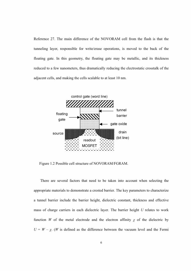
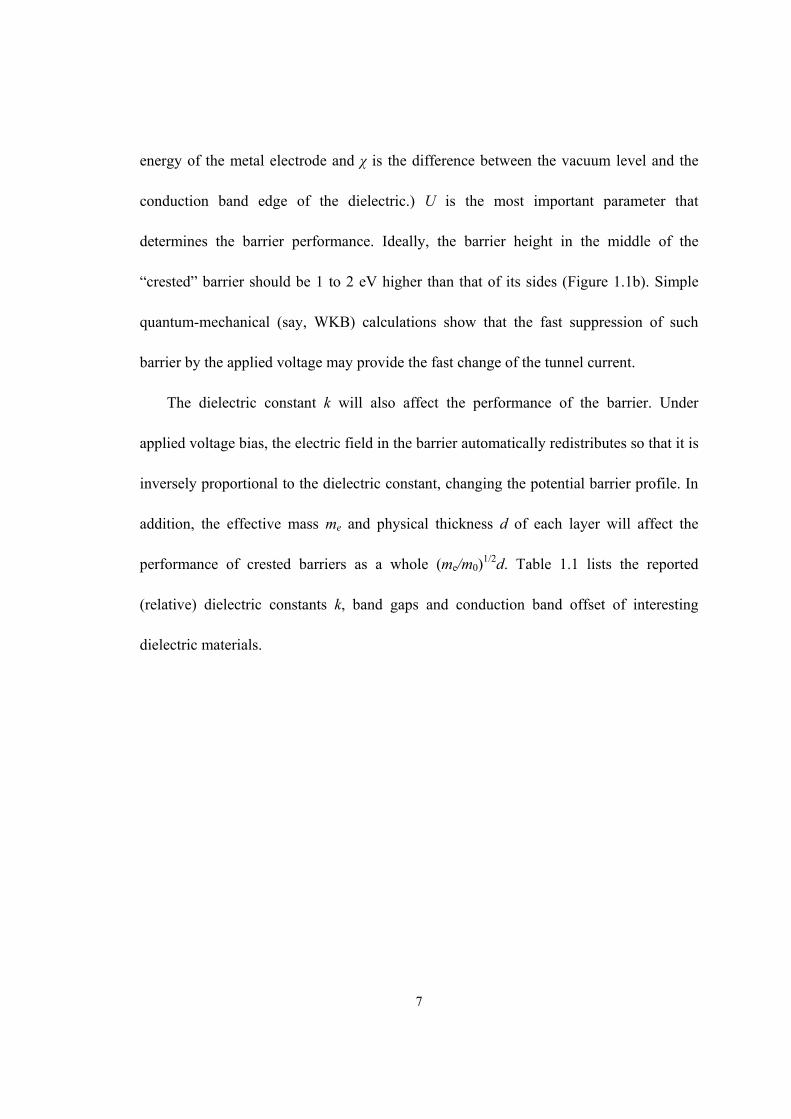


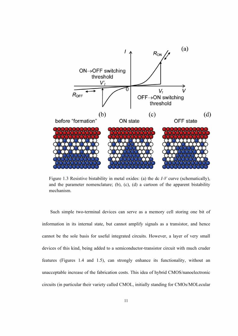
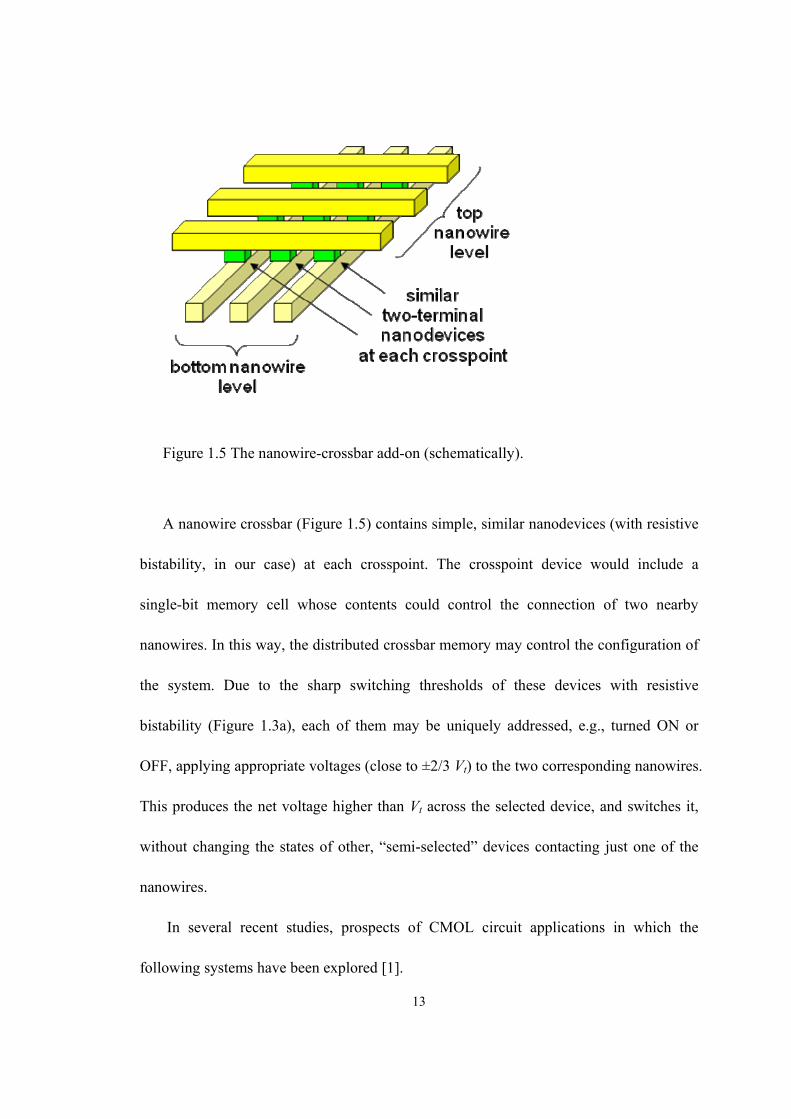


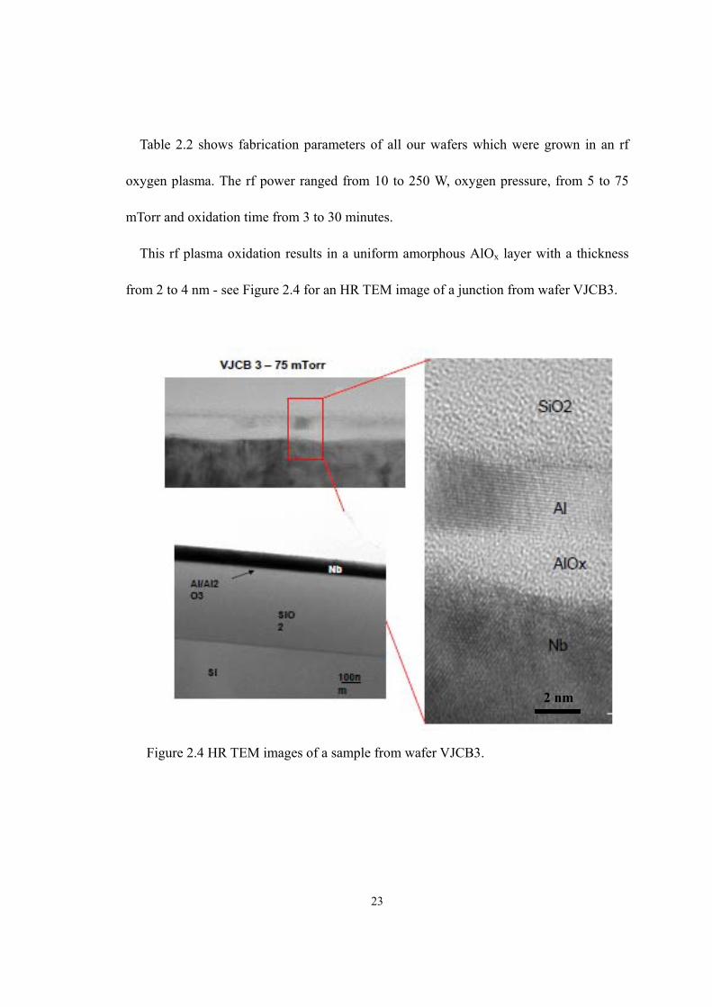


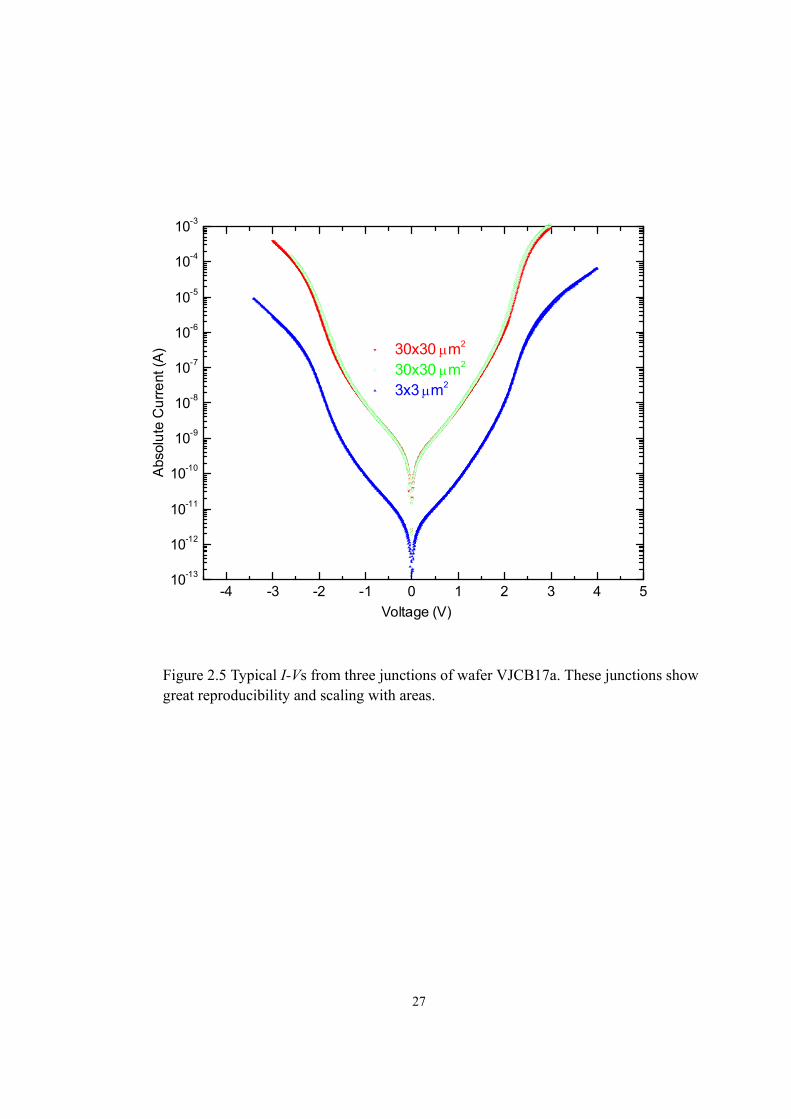

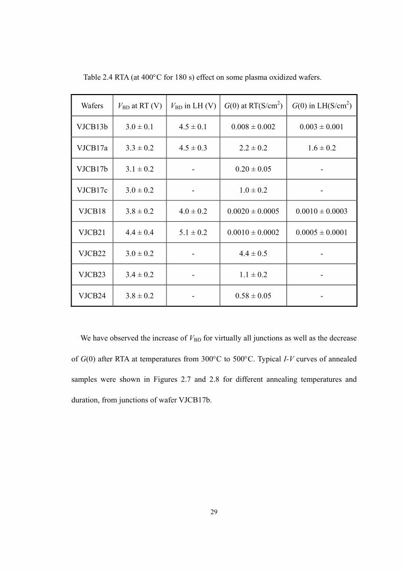
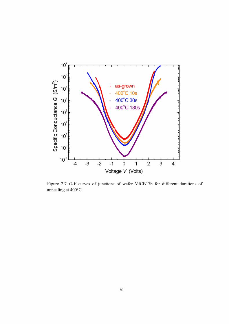
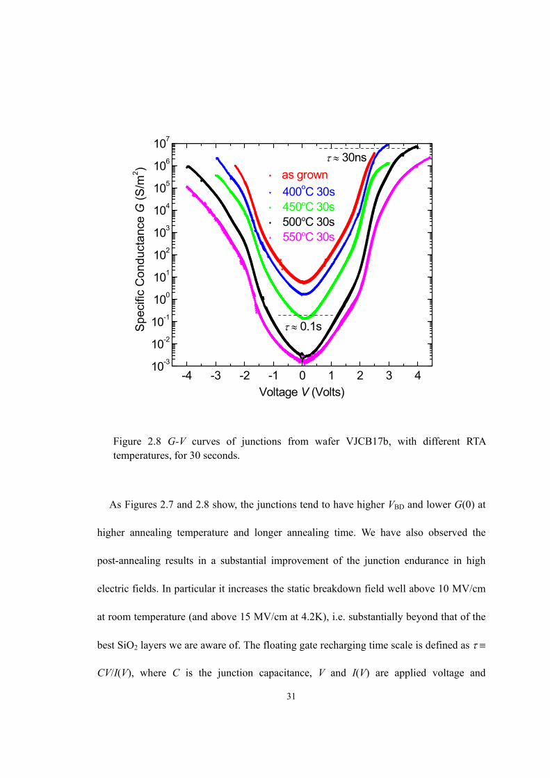


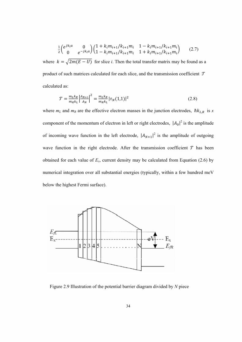

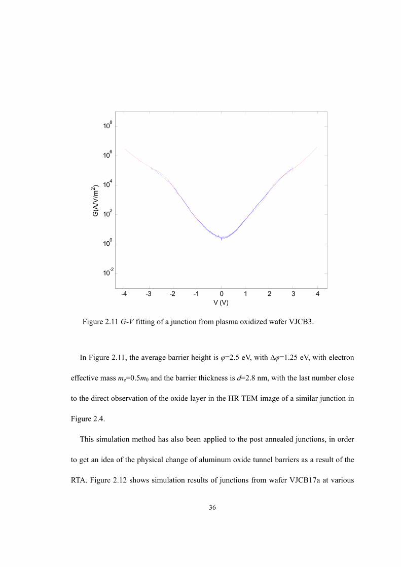


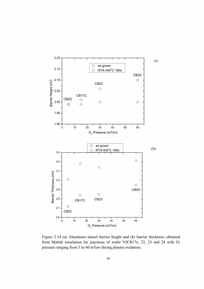
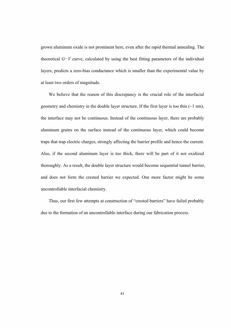


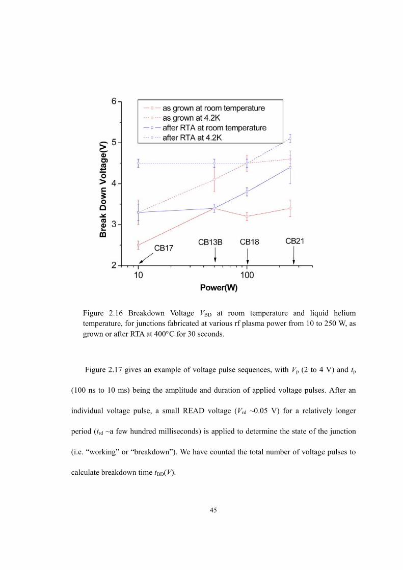
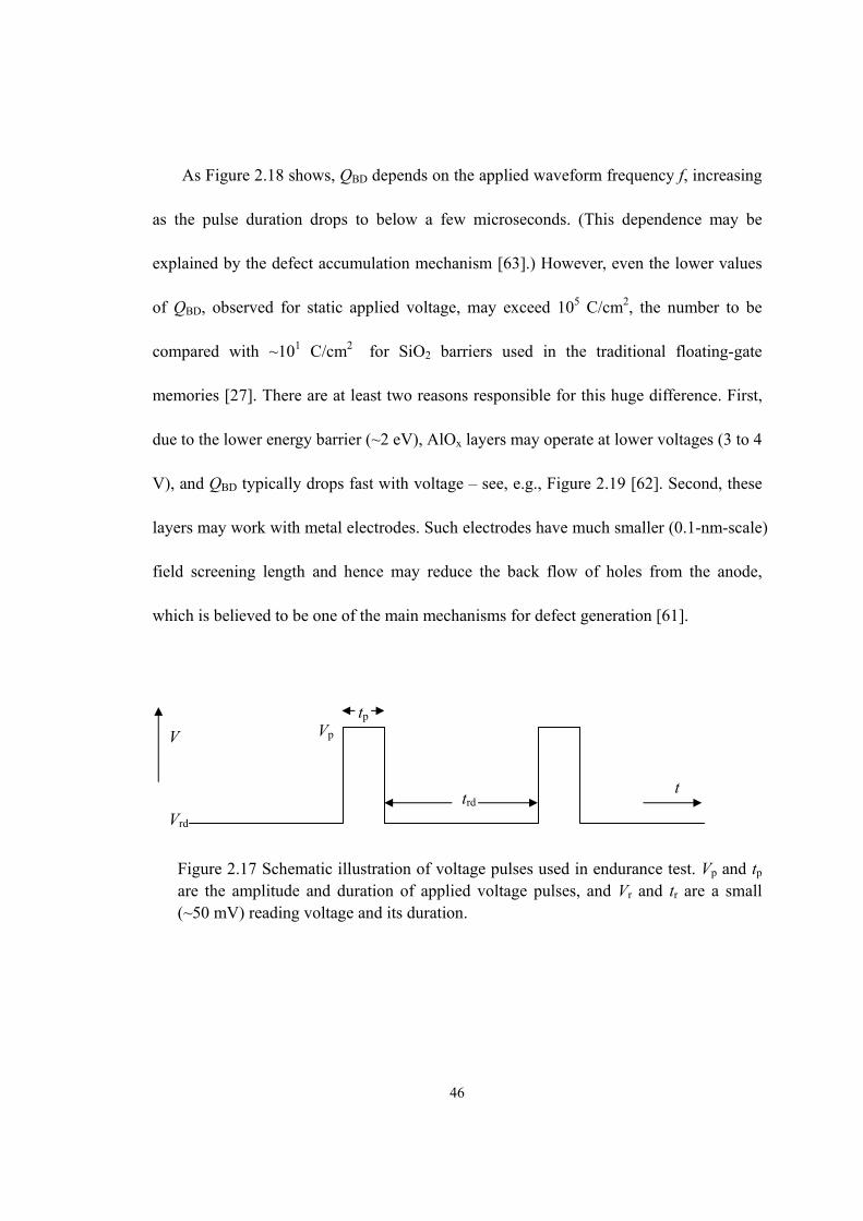

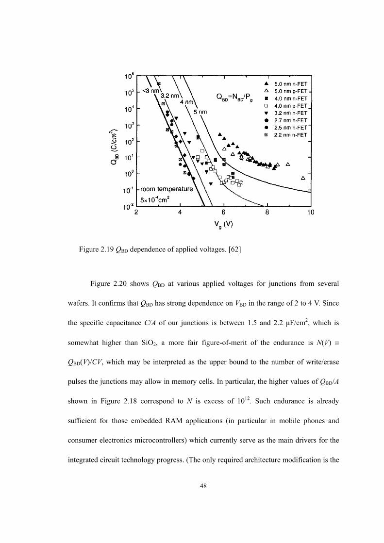
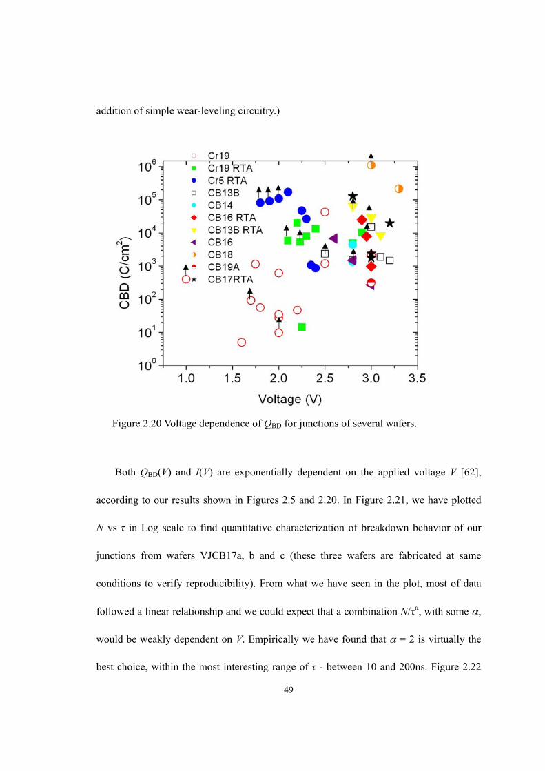


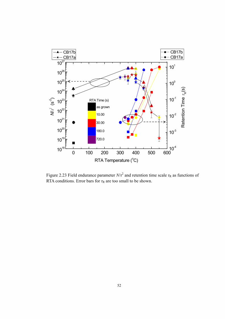


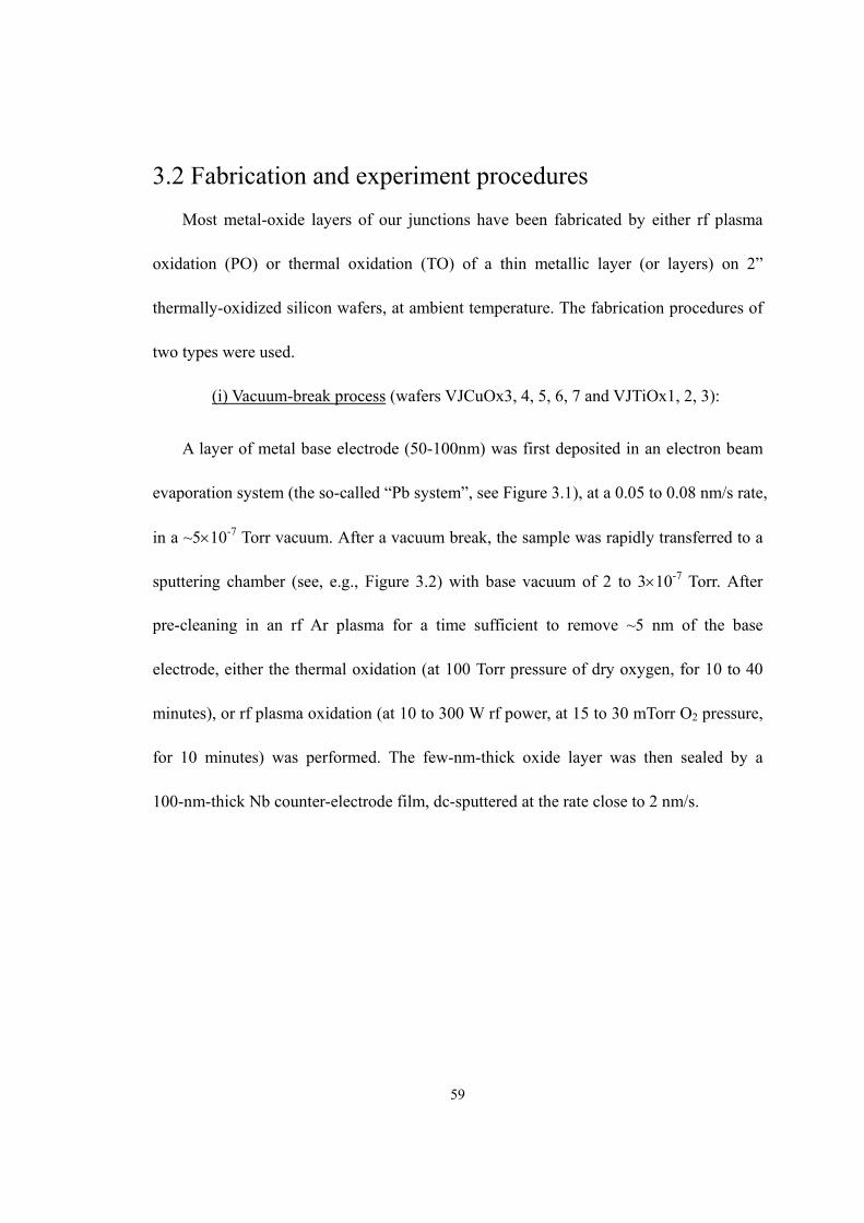
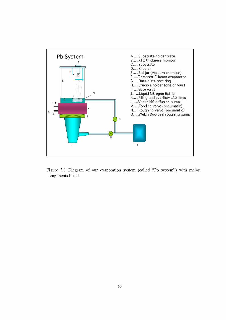


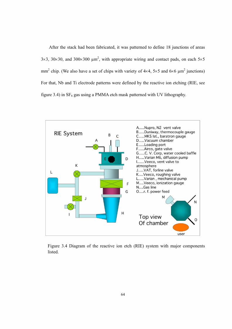


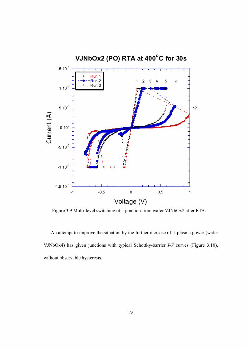


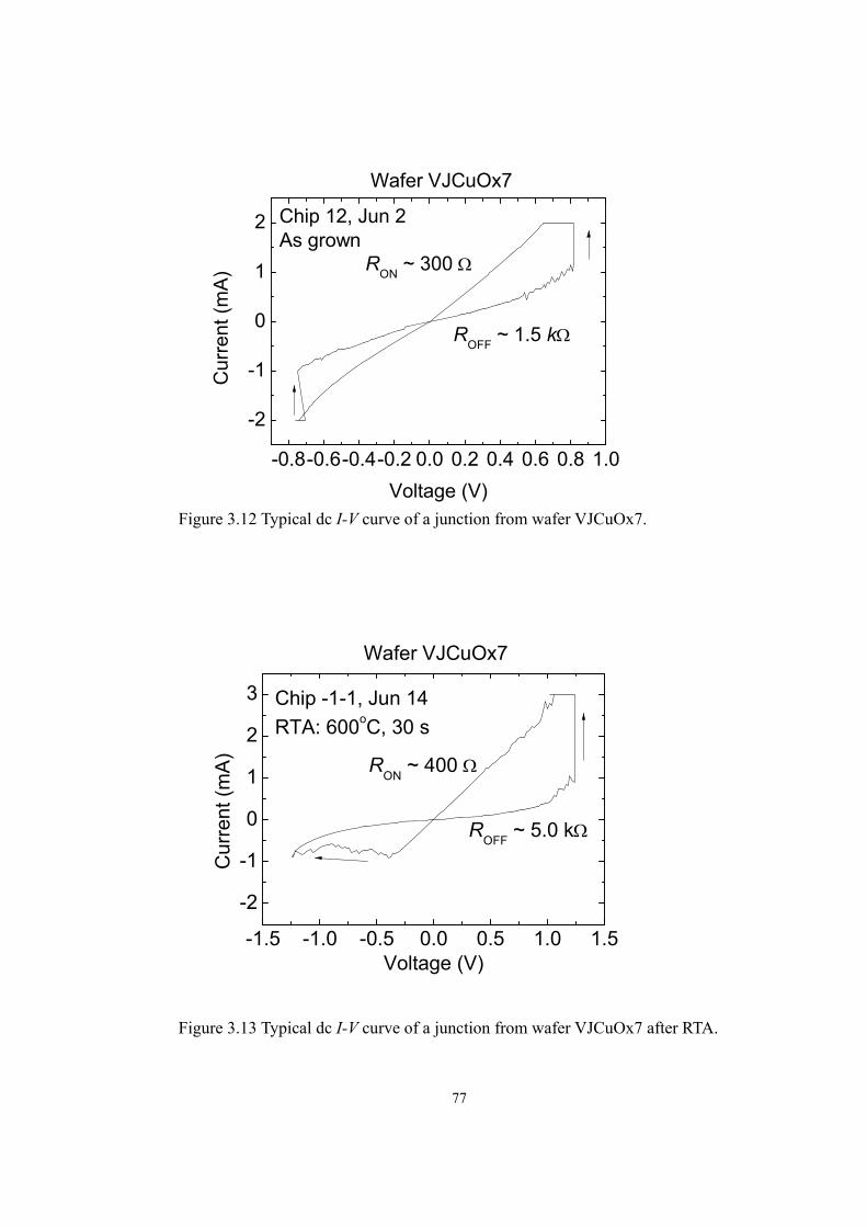
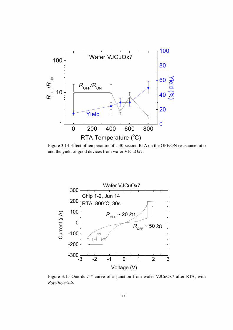
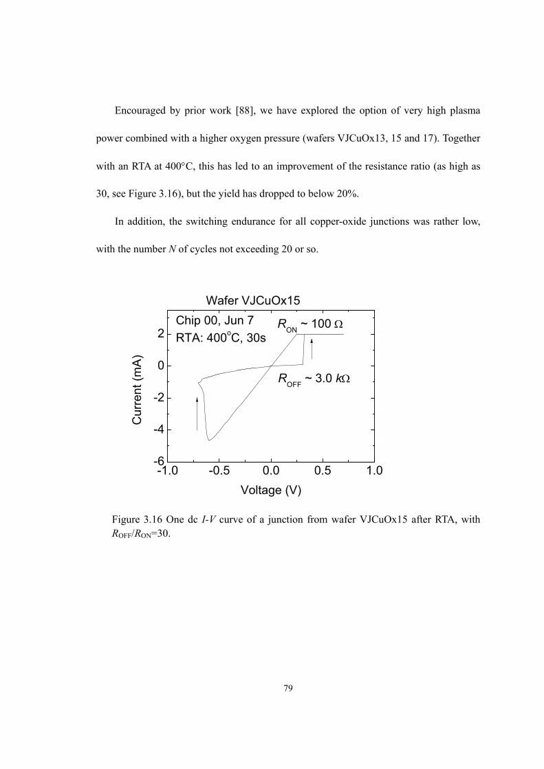

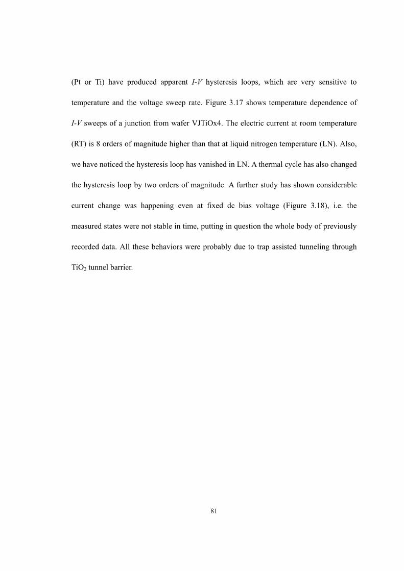
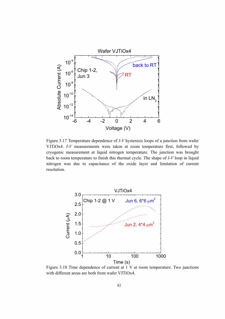
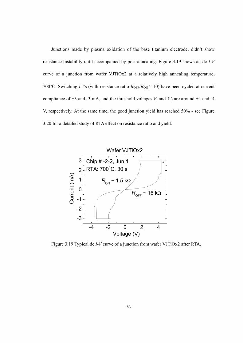

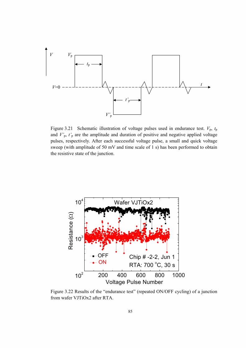


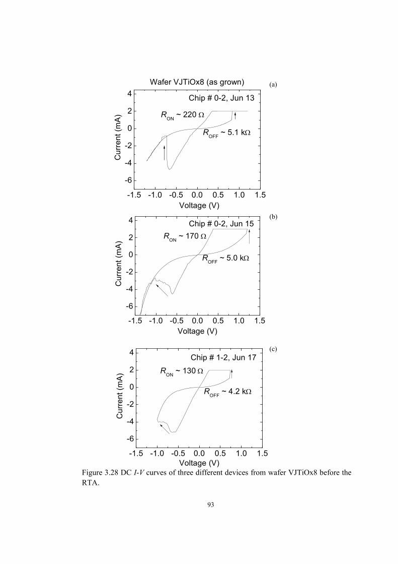

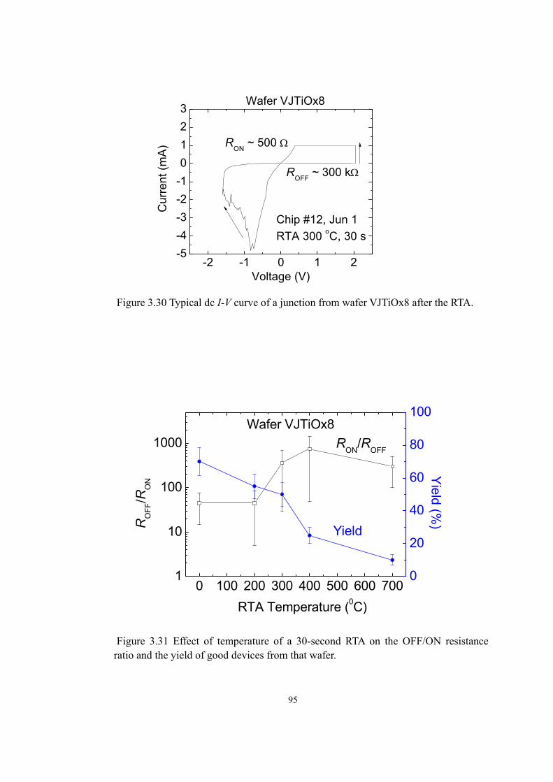


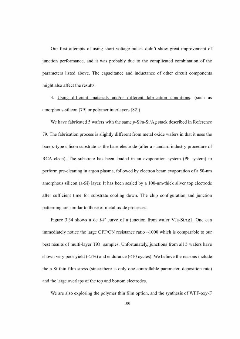


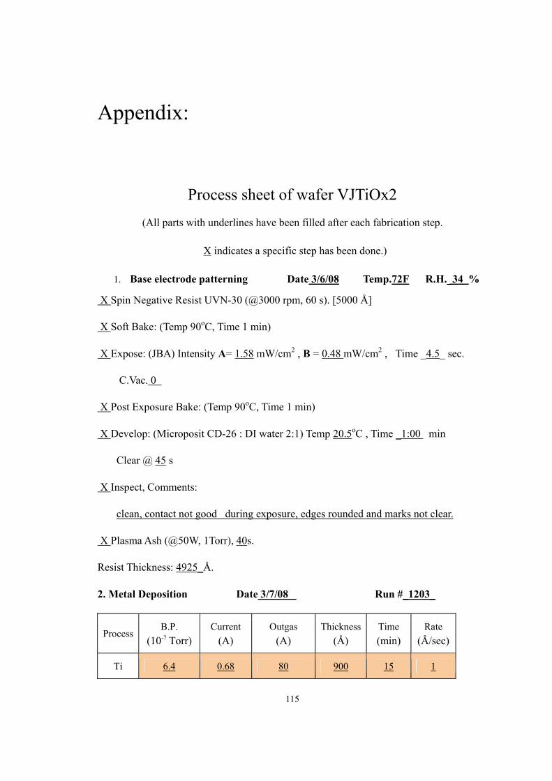


![2.3.1 Enthalpy Changes - Physics & Maths Tutorpmt.physicsandmathstutor.com/download/Chemistry/A-level/Topic-Qs... · ... CH 3(CH 2)4OH. In the experiment, 1.76 g of ... –1 [3] [Total](https://static.documents.pub/doc/80x56/5ad263837f8b9a72118d18b1/231-enthalpy-changes-physics-maths-ch-3ch-24oh-in-the-experiment.jpg)
