+ All Categories
Home > Documents > 1 Emission and Excitation Mechanisms of Phosphors · Luminescent materials, also called phosphors,...

1 Emission and Excitation Mechanisms of Phosphors · Luminescent materials, also called phosphors,...

Date post: 26-May-2020
Category:
Upload: others
View: 4 times
Download: 0 times
Share this document with a friend
34
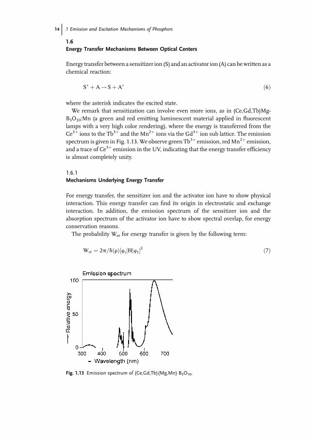
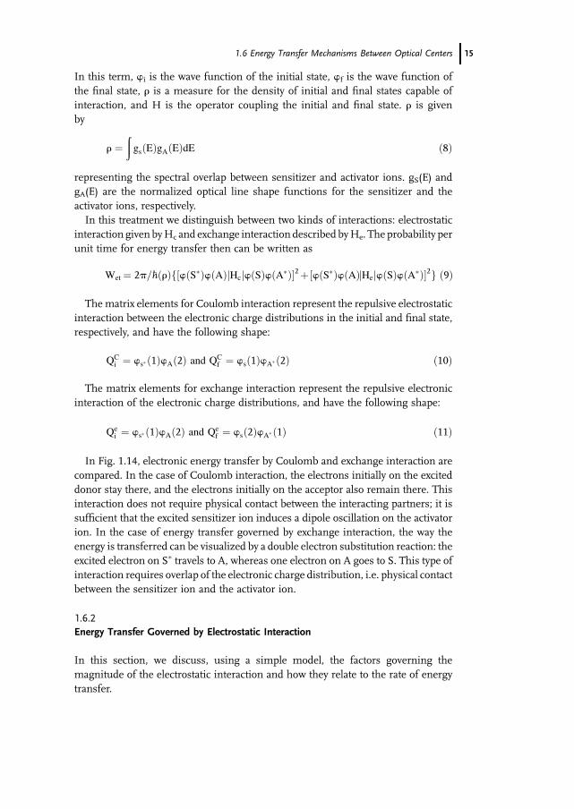
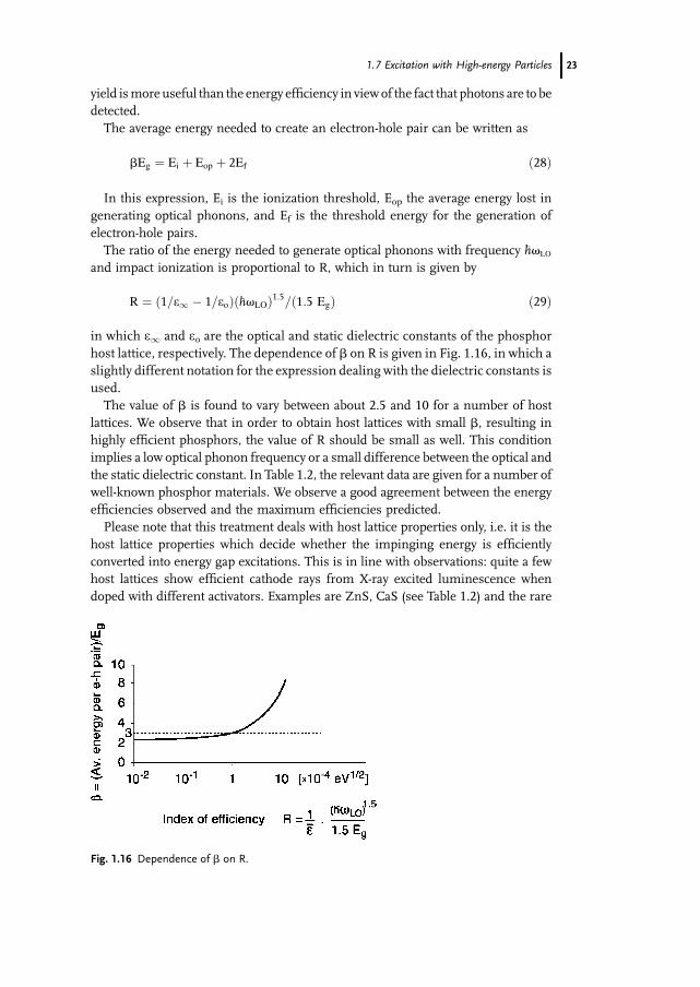
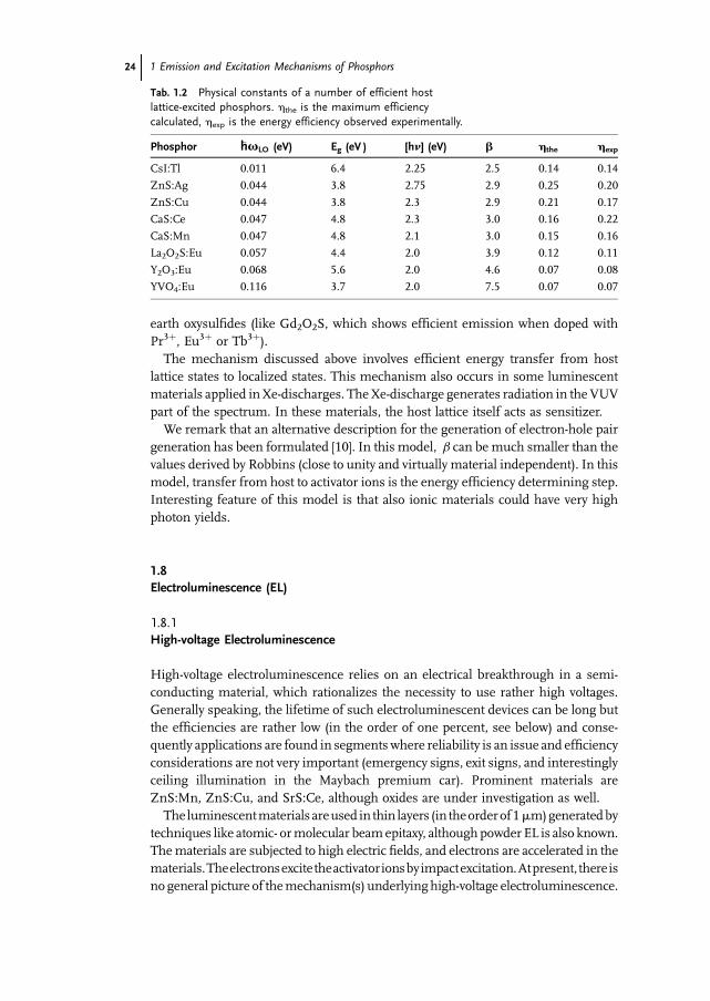
1 Emission and Excitation Mechanisms of Phosphors Cees R. Ronda 1.1 Introduction In this chapter, basic concepts involved in luminescence will be discussed. We will take a closer look at a number of excitation mechanisms which are involved in generating luminescence and processes which lead to luminescence, taking illustrative examples from luminescent materials applied in fluorescent lamps and cathode ray tubes. With respect to fluorescent lamps, we will restrict ourselves to discharge lamps based on the low-pressure Hg discharge. Other applications will be treated more extensively in separate chapters. A separate chapter in this book is devoted to scintillators, used in medical detectors. Here the excitation mechanism strongly resembles the one in cathode ray phosphors. Phosphors for Light-Emitting Diodes (LEDs) and phosphors for Plasma Display Panels (PDPs) are treated separately as well, the processes leading to excitation and emission being comparable to those in fluorescent lamps. Possible ways to influence the emission color will be discussed, this being of strong relevance for applications. We will also give an overview of the most popular devices that rely on luminescent materials, and finally we will touch upon processes that result in nonradiative recombination. Recently, organic luminescent materials have attracted considerable interest in view of their application in organic light-emitting diodes. In this chapter, however, we discuss inorganic phosphors only. 1.2 General Considerations – Fluorescent Lamps On passing a current through an Hg discharge, UV light is generated as a consequence of electronic transitions on the Hg atoms. In low-pressure Hg discharge, the main emission line is located at 254 nm. This light is invisible and harmful; therefore it has to be converted into visible light. This is done by the application of luminescent materials. These materials have to show a strong absorption at 254 nm and have to convert this into visible light very efficiently. In most of the fluorescent lamp phosphors, the optical Luminescence: From Theory to Applications. Edited by Cees Ronda Copyright ß 2008 WILEY-VCH Verlag GmbH & Co. KGaA, Weinheim ISBN: 978-3-527-31402-7 1
Transcript

1

Emission and Excitation Mechanisms of PhosphorsCees R. Ronda

1.1

Introduction

In this chapter, basic concepts involved in luminescencewill be discussed.Wewill take

a closer look at a number of excitation mechanisms which are involved in generating

luminescence and processes which lead to luminescence, taking illustrative examples

from luminescentmaterials applied in fluorescent lamps and cathode ray tubes.With

respect to fluorescent lamps, we will restrict ourselves to discharge lamps based on

the low-pressure Hg discharge. Other applications will be treated more extensively

in separate chapters. A separate chapter in this book is devoted to scintillators, used in

medical detectors. Here the excitation mechanism strongly resembles the one in

cathode ray phosphors. Phosphors for Light-Emitting Diodes (LEDs) and phosphors

for Plasma Display Panels (PDPs) are treated separately as well, the processes leading

to excitation and emission being comparable to those in fluorescent lamps.

Possibleways to influence the emission colorwill be discussed, this being of strong

relevance for applications. We will also give an overview of the most popular devices

that rely on luminescent materials, and finally we will touch upon processes that

result in nonradiative recombination.

Recently, organic luminescent materials have attracted considerable interest in

view of their application in organic light-emitting diodes. In this chapter, however, we

discuss inorganic phosphors only.

1.2

General Considerations – Fluorescent Lamps

Onpassing a current throughanHgdischarge,UV light is generated as a consequence

of electronic transitions on the Hg atoms. In low-pressure Hg discharge, the main

emission line is locatedat254nm.This light is invisibleandharmful; therefore ithas to

be converted into visible light. This is doneby theapplicationof luminescentmaterials.

Thesematerialshavetoshowastrongabsorptionat254nmandhavetoconvert this into

visible light very efficiently. In most of the fluorescent lamp phosphors, the optical

Luminescence: From Theory to Applications. Edited by Cees RondaCopyright � 2008 WILEY-VCH Verlag GmbH & Co. KGaA, WeinheimISBN: 978-3-527-31402-7

1

processes leading to luminescence do not involve host lattice states, implying that the

energy gap is at least 4.9 eV, this being the energy of a photonwithwavelength 254nm.

Therefore, the luminescent materials applied in fluorescent lamps are insulators.

The conversion efficiency of luminescent materials is very high: about 90% of the

UVphotons are absorbed, and also about 90%of the absorbed photons are converted

into visible light. This implies that suchmaterials cannot be improved any further in

terms of conversion efficiency unlessmaterials can be found that generatemore than

one visible photon after absorption of a UV photon. This is the subject of a separate

chapter in this book.

An elementary calculation shows that, even though fluorescent lamps are themost

efficient white light sources, the overall energy efficiency is nevertheless rather

limited: only about 25%. The percentage energy efficiency is calculated as follows:

h ¼ hdisch �hphos � ð254=550Þ �100 ð1Þ

in which 254 nm is the wavelength of the exciting Hg radiation in nm and 550 nm is

the mean wavelength of the light emitted. As in current fluorescent lamp phosphors

only one visible photon per absorbed UV photon is generated, the difference in

photon energy represents energy loss. The discharge efficiency (hdisch) of the Hg

discharge is about 70% and the conversion efficiency (hphos) of the phosphors (on a

photon basis) is about 80%. Insertion of these numbers leads to the overall efficiency

of about 25%. In view of the very high Hg discharge efficiency, here also hardly any

significant improvement can be expected. This implies that this lamp concept has

reached physical limits in terms of energy efficiency.

Compact fluorescent lamps have a lower light generation efficiency (only 15%). As

the luminescent materials applied are the same or very similar, this must due to the

lower discharge efficiency in these devices, which, in turn, is due to the smaller

diameter of the lamp envelope and therefore to the increased wall losses: excited Hg

atoms reach the ground state on interacting with the lamp wall without generating

UV light: energy and momentum can be conserved by interaction of excited species

with the wall without generation of light.

1.3

General Considerations – Cathode Ray Tubes

Though the importance of cathode ray tubes is rapidly decreasing, we will treat the

luminescence mechanism in these materials in view of its historical importance. In

addition, the excitation mechanism that comprises excitation with high-energy

particles (electrons, X-ray photons, or g-rays) is also operative in phosphors used

in scintillators for, e.g., medical applications.

Luminescent materials applied in cathode ray tubes in general differ from those

applied in fluorescent lamps. Excitation proceeds via the band gap. To achieve high

efficiencies, small values for the band gap are needed, as will be elucidated below. For

this reason, quite a few luminescent materials applied in cathode ray tubes are

semiconductors.

2 1 Emission and Excitation Mechanisms of Phosphors

The luminescence mechanism operating in the blue and green emitting phos-

phors applied in cathode ray tubes is a beautiful example of luminescence involving

defect states in semiconductors. We will therefore also discuss this mechanism in

some detail.

The maximum energy efficiency of the cathode ray phosphors is relatively low, at

most about 25%, as will be outlined in this chapter. Also for these phosphors, the

maximum efficiencies have been reached.

In the next sections, we will deal with luminescence and excitation mechanisms.

1.4

Luminescence Mechanisms

Luminescent materials, also called phosphors, are mostly solid inorganic materials

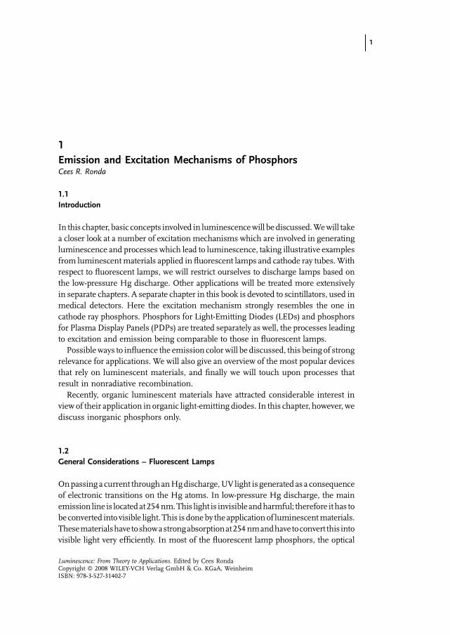
consisting of a host lattice, usually intentionally doped with impurities (see Fig. 1.1).

The impurity concentrations generally are low in view of the fact that at higher

concentrations the efficiency of the luminescence process usually decreases (con-

centration quenching, see below). In addition, most of the phosphors have a white

body color. Especially for fluorescent lamps, this is an essential feature to prevent

absorption of visible light by the phosphors used. The absorption of energy, which is

used to excite the luminescence, takes place by either the host lattice or by intentionally

doped impurities. Inmost cases, the emission takes place on the impurity ions,which,

when they also generate the desired emission, are called activator ions. When the

activator ions show too weak an absorption, a second kind of impurities can be added

(sensitizers), which absorb the energy and subsequently transfer the energy to the

activators. This process involves transport of energy through the luminescent mater-

ials. Quite frequently, the emission color can be adjusted by choosing the proper

impurity ion, without changing the host lattice in which the impurity ions are

incorporated. On the other hand, quite a few activator ions show emission spectra

with emission at spectral positions which are hardly influenced by their chemical

environment. This is especially true for many of the rare-earth ions.

Fig. 1.1 Luminescent material containing activator ions A (ions showing

the desired emission) and sensitizing ions S (on which, e.g., UV excitation

can take place).

1.4 Luminescence Mechanisms 3

1.4.1

Center Luminescence

In the case of center luminescence, the emission is generated on an optical center, in

contradiction to, e.g., emission, which results from optical transitions between host

lattice band states or froma transition between two centers. Such anoptical center can

be an ion or a molecular ion complex.

One speaks of characteristic luminescence when, in principle, the emission could

also occur on the ion in a vacuum, i.e. when the optical transition involves electronic

states of the ion only. Characteristic luminescence can consist of relatively sharp

emission bands (spectral width typically a few nm), but also of broad bands, which

can have widths exceeding 50 nm in the visible part of the spectrum. Broad emission

bands are observed when the character of the chemical bonding in the ground and

excited state differs considerably. This goes hand in hand with a change in equili-

brium distance between the emitting ion and its immediate chemical environment

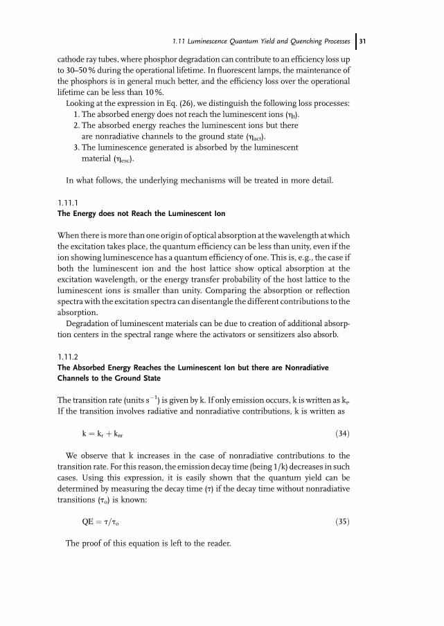
and is commonly explained with the configuration coordinate diagram (Fig. 1.2).

In this diagram, Qg andQe represent themetal-ligand distances in the ground and

excited states, respectively. Ea and Ee are the energies at which the absorption and

emission bands have theirmaximum intensity, respectively.D is the energy of the so-

called zero phonon line; this transition involves completely relaxed excited and

ground states, and no excited phonon states are involved – hence the name of this

kind of transitions. The phonon frequencies in the ground and excited state are given

by �hvg and �hve, respectively. The relaxation energies in the ground and excited states

can be expressed as a product of the phonon energy and the so-called Huang-Rhys

factors. TheHuang-Rhys factors Se and Sg in the ground and excited state (being pure

numbers), respectively, give themean number of phonons involved in the absorption

and emission processes, respectively. In the harmonic approximation, the curvature

of the parabolic band (determined by the bond strength), the phonon frequencies,

and theHuang-Rhys factors are the same in the ground and excited state. This picture

Fig. 1.2 Configurational coordinate diagram.

4 1 Emission and Excitation Mechanisms of Phosphors

is very elementary. For example, it does not describe thermal expansion of the lattice.

However, it does give a lot of insight. It can, e.g., be used in showing that a larger

Stokes Shift is expected on increasing lattice relaxation and also in the description of

thermal quenching of the emission (see further below).

Broad bands are observed for many optical transitions in the partly filled d-shell of

transitionmetal ions (d! d transitions), but also for transitions between the 5d shell

and the 4f shell of rare-earth ions (d! f transitions) and for emission on s2 ions

(these ions possess a ‘‘lone pair’’ of s electrons), like Tlþ, Pb2þ, or Sb3þ. Sharp

emission bands are characteristic of optical transitions between electronic states with

chemical bonding character (almost) the same for ground and excited state, and for

the same reason also of optical transitions between electronic states that hardly

participate in the chemical bonding (e.g., f! f transitions on rare-earth ions).

In the case of optical processes involving electronic states which participate in the

chemical bonding, the nature of the bonding (covalent, ionic) and the symmetry of

the site at which the emitting ion is incorporated play a very important role. This is

generally described by the ligand field theory, which we do not treat here.We will use

the term symbols for the description of the electronic transitionswhich arise from the

site symmetry of the ions of interest, however.

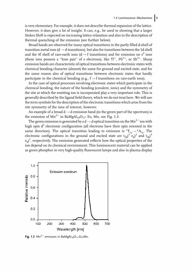
An example of a broad d! d emission band (in the green part of the spectrum) is

the emission of Mn2þ in BaMgAl10O17: Eu, Mn, see Fig. 1.3.

The green emission is generated by a d! d optical transition on theMn2þ ionwith

high spin d5 electronic configuration (all electrons have their spin oriented in the

same direction). The optical transition leading to emission is 4T1g ! 6A1g. The

electronic configurations in the ground and excited state are t2g)3 eg)

2 and t2g)4

eg)1, respectively. The emission generated reflects how the optical properties of the

ion depend on its chemical environment. This luminescent material can be applied

as green phosphor in very high-quality fluorescent lamps and also in plasma display

Fig. 1.3 Mn2þ emission in BaMgAl10O17:Eu,Mn.

1.4 Luminescence Mechanisms 5

panels. Its quantumefficiency is very high (90%), and it shows a very good absorption

at 254 nm, the absorption taking place on the Eu2þ ion, followed by energy transfer to

Mn2þ. This process is elucidated further below. The composition without Mn2þ

shows efficient blue Eu2þ emission; this emission is responsible for the shoulder at

450 nmand is used as blue emitting phosphor in high-quality fluorescent lamps. The

emission stems from the optically allowed 5d-4f transition on Eu2þ, which is

consequently very fast (decay time about 1ms). Sr5(PO4)3Cl:Eu shows virtually the

same emission band, and is used in high-quality fluorescent lamps as well.

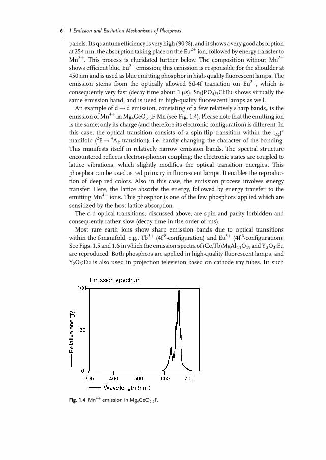
An example of d! d emission, consisting of a few relatively sharp bands, is the

emission ofMn4þ inMg4GeO5.5F:Mn (see Fig. 1.4). Please note that the emitting ion

is the same; only its charge (and therefore its electronic configuration) is different. In

this case, the optical transition consists of a spin-flip transition within the t2g)3

manifold (2E! 4A2 transition), i.e. hardly changing the character of the bonding.

This manifests itself in relatively narrow emission bands. The spectral structure

encountered reflects electron-phonon coupling: the electronic states are coupled to

lattice vibrations, which slightly modifies the optical transition energies. This

phosphor can be used as red primary in fluorescent lamps. It enables the reproduc-

tion of deep red colors. Also in this case, the emission process involves energy

transfer. Here, the lattice absorbs the energy, followed by energy transfer to the

emitting Mn4þ ions. This phosphor is one of the few phosphors applied which are

sensitized by the host lattice absorption.

The d-d optical transitions, discussed above, are spin and parity forbidden and

consequently rather slow (decay time in the order of ms).

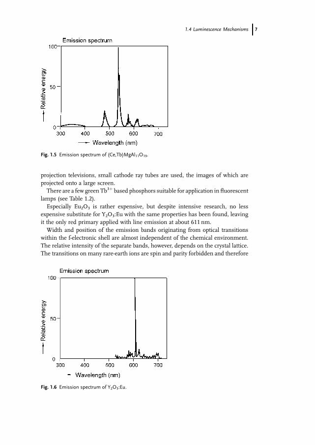
Most rare earth ions show sharp emission bands due to optical transitions

within the f-manifold, e.g., Tb3þ (4f 8-configuration) and Eu3þ (4f 6-configuration).

See Figs. 1.5 and 1.6 inwhich the emission spectra of (Ce,Tb)MgAl11O19 andY2O3:Eu

are reproduced. Both phosphors are applied in high-quality fluorescent lamps, and

Y2O3:Eu is also used in projection television based on cathode ray tubes. In such

Fig. 1.4 Mn4þ emission in Mg4GeO5.5F.

6 1 Emission and Excitation Mechanisms of Phosphors

projection televisions, small cathode ray tubes are used, the images of which are

projected onto a large screen.

There are a few green Tb3þ based phosphors suitable for application in fluorescent

lamps (see Table 1.2).

Especially Eu2O3 is rather expensive, but despite intensive research, no less

expensive substitute for Y2O3:Eu with the same properties has been found, leaving

it the only red primary applied with line emission at about 611 nm.

Width and position of the emission bands originating from optical transitions

within the f-electronic shell are almost independent of the chemical environment.

The relative intensity of the separate bands, however, depends on the crystal lattice.

The transitions on many rare-earth ions are spin and parity forbidden and therefore

Fig. 1.5 Emission spectrum of (Ce,Tb)MgAl11O19.

Fig. 1.6 Emission spectrum of Y2O3:Eu.

1.4 Luminescence Mechanisms 7

rather slow (in the ms range). However, for a number of rare-earth ions, broad

emission bands are also known, due to d! f emission, e.g., Eu2þ (4f 7-configuration)

or Ce3þ (4f 1-configuration). These transitions are allowed and consequently very fast

(in the ms range or even faster).

Quite a few very important commercial phosphors are based on rare-earth ions.

Rare-earth based phosphors are frequently applied in very demanding applications.

1.4.2

Charge Transfer Luminescence

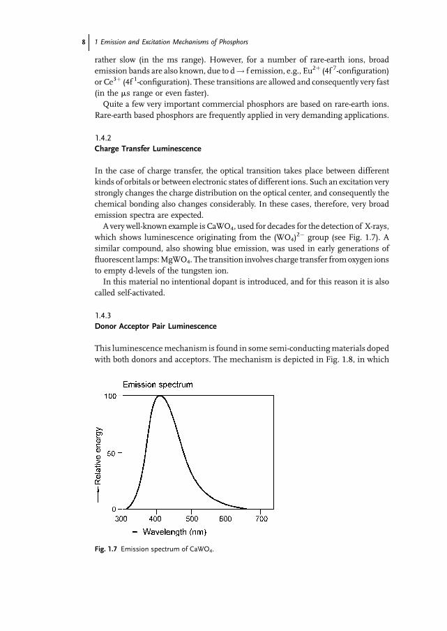
In the case of charge transfer, the optical transition takes place between different

kinds of orbitals or between electronic states of different ions. Such an excitation very

strongly changes the charge distribution on the optical center, and consequently the

chemical bonding also changes considerably. In these cases, therefore, very broad

emission spectra are expected.

A very well-known example is CaWO4, used for decades for the detection of X-rays,

which shows luminescence originating from the (WO4)2� group (see Fig. 1.7). A

similar compound, also showing blue emission, was used in early generations of

fluorescent lamps:MgWO4. The transition involves charge transfer fromoxygen ions

to empty d-levels of the tungsten ion.

In this material no intentional dopant is introduced, and for this reason it is also

called self-activated.

1.4.3

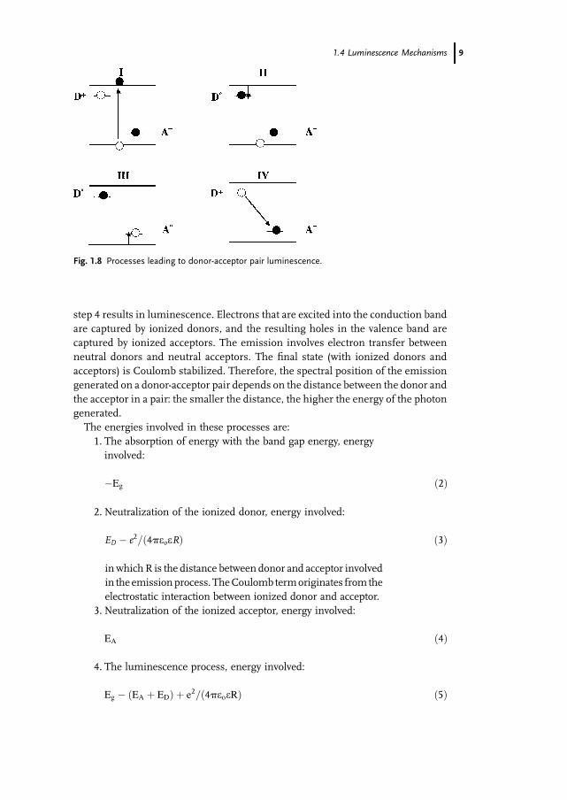
Donor Acceptor Pair Luminescence

This luminescencemechanism is found in some semi-conductingmaterials doped

with both donors and acceptors. The mechanism is depicted in Fig. 1.8, in which

Fig. 1.7 Emission spectrum of CaWO4.

8 1 Emission and Excitation Mechanisms of Phosphors

step 4 results in luminescence. Electrons that are excited into the conduction band

are captured by ionized donors, and the resulting holes in the valence band are

captured by ionized acceptors. The emission involves electron transfer between

neutral donors and neutral acceptors. The final state (with ionized donors and

acceptors) is Coulomb stabilized. Therefore, the spectral position of the emission

generated on a donor-acceptor pair depends on the distance between the donor and

the acceptor in a pair: the smaller the distance, the higher the energy of the photon

generated.

The energies involved in these processes are:

1. The absorption of energy with the band gap energy, energy

involved:

�Eg ð2Þ

2. Neutralization of the ionized donor, energy involved:

ED � e2=ð4peoeRÞ ð3Þ

in which R is the distance between donor and acceptor involved

in the emissionprocess. TheCoulomb termoriginates from the

electrostatic interaction between ionized donor and acceptor.

3. Neutralization of the ionized acceptor, energy involved:

EA ð4Þ

Fig. 1.8 Processes leading to donor-acceptor pair luminescence.

4. The luminescence process, energy involved:

Eg � ðEA þ EDÞ þ e2=ð4peoeRÞ ð5Þ

1.4 Luminescence Mechanisms 9

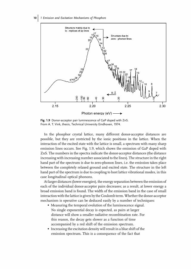
In the phosphor crystal lattice, many different donor-acceptor distances are

possible, but they are restricted by the ionic positions in the lattice. When the

interaction of the excited state with the lattice is small, a spectrum with many sharp

emission lines occurs. See Fig. 1.9, which shows the emission of GaP doped with

ZnS. The numbers in the spectra indicate the donor-acceptor distances (the distance

increasing with increasing number associated to the lines). The structure in the right

hand part of the spectrum is due to zero-phonon lines, i.e. the emission takes place

between the completely relaxed ground and excited state. The structure in the left

hand part of the spectrum is due to coupling to host lattice vibrational modes, in this

case longitudinal optical phonons.

At larger distances (lower energies), the energy separation between the emission of

each of the individual donor-acceptor pairs decreases; as a result, at lower energy a

broad emission band is found. The width of the emission band in the case of small

interactionwith the lattice is given by theCoulomb term.Whether the donor-acceptor

mechanism is operative can be deduced easily by a number of techniques:� Measuring the temporal evolution of the luminescence signal.

No single exponential decay is expected, as pairs at larger

distance will show a smaller radiative recombination rate. For

this reason, the decay gets slower as a function of time

accompanied by a red shift of the emission spectrum.� Increasing the excitation density will result in a blue shift of the

emission spectrum. This is a consequence of the fact that

Fig. 1.9 Donor-acceptor pair luminescence of GaP doped with ZnS.

From A. T. Vink, thesis, Technical University Eindhoven, 1974.

10 1 Emission and Excitation Mechanisms of Phosphors

emissions at short donor-acceptor pair distances, which have

the highest photon energy, have the shortest decay time.

The more distant pairs decay much more slowly than the

pairs at short distances. Consequently, the more distant

pairs saturate, i.e. contribute less to the emission, which

rationalizes the blue shift.

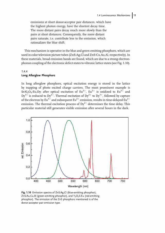
This mechanism is operative in the blue and green emitting phosphors, which are

used in color television picture tubes (ZnS:Ag,Cl and ZnS:Cu,Au,Al, respectively). In

these materials, broad emission bands are found, which are due to a strong electron-

phonon coupling of the electronic defect states to vibronic lattice states (see Fig. 1.10).

1.4.4

Long Afterglow Phosphors

In long afterglow phosphors, optical excitation energy is stored in the lattice

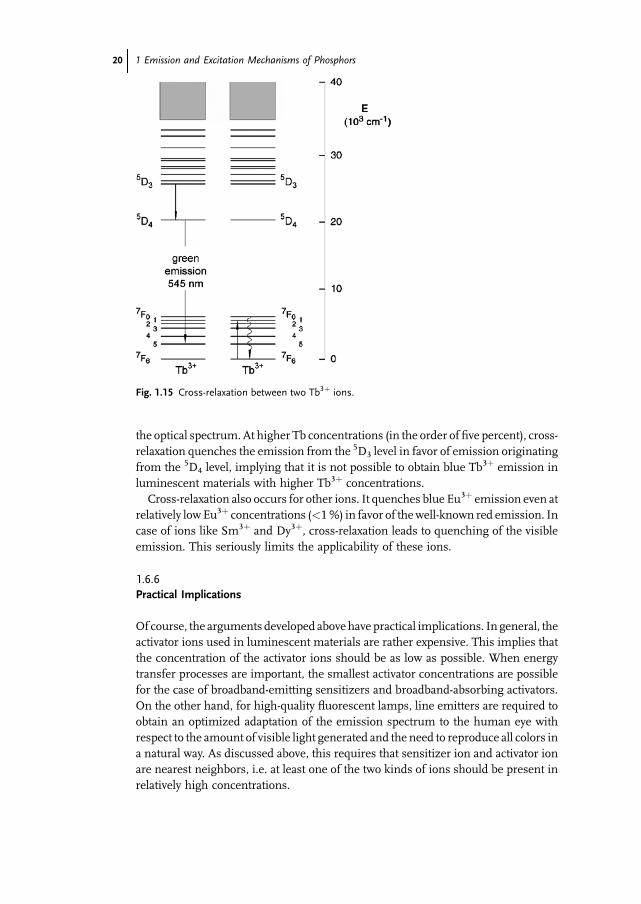
by trapping of photo excited charge carriers. The most prominent example is

SrAl2O4:Eu,Dy: after optical excitation of Eu2þ, Eu2þ is oxidized to Eu3þ and

Dy3þ is reduced to Dy2þ. Thermal excitation of Dy2þ to Dy3þ, followed by capture

of the electron by Eu3þ and subsequent Eu2þ emission, results in time-delayed Eu2þ

emission. The thermal excitation process of Dy2þ determines the time delay. This

particular material still generates visible emission after several hours in the dark.

Fig. 1.10 Emission spectra of ZnS:Ag,Cl (blue-emitting phosphor),

ZnS:Au,Cu,Al (green-emitting phosphor), and Y2O2S:Eu (red-emitting

phosphor). The emission of the ZnS phosphors mentioned is of the

donor-acceptor pair emission type.

1.4 Luminescence Mechanisms 11

The samemechanism also leads to (undesired) afterglow in scintillatingmaterials,

e.g., in Gd2O2S:Pr,Ce, which is used in Computer Tomography (CT) equipment.

Long afterglow phosphors can be used in watch fingers, but also in safety

applications, e.g., in exit signs which still operate in case of a current blackout.

Other long afterglow materials are, e.g., ZnS:Cu and SrS:Bi.

When the energy involved in reversing the trapping process thermally is too high,

IR-light absorption might be used to generate visible luminescence. This is the

mechanismunderlying the use of BaFBr:Eu asX-ray phosphor, aswill be discussed in

the chapter on scintillators.

1.5

Excitation Mechanisms

1.5.1

Optical Excitation of Luminescence and Energy Transfer

When absorption of UVor even visible light leads to emission, one speaks of optical

excitation of luminescence. This process takes place in, e.g., fluorescent lamps and

phosphor-converted LEDs, in which phosphors are used to at least partly change the

wavelength of the radiation emitted by the LED. Optical absorption can take place on

the already discussed impurities (optical centers), being either the activator ions or

the sensitizer ions. Sensitizer ions are used when the optical absorption of the

activator ions is tooweak (e.g., because the optical transition is forbidden) to be useful

in practical devices. In such a case, energy transfer from the sensitizer ions to the

activator ions has to take place. The optical absorption leading to emission can also

take place by the host lattice itself (band absorption). In this case one speaks of host

lattice sensitization. Energy transfer from host lattice states to the activator ions (in

some cases also involving sensitizers) has to take place.

In the blue emitting luminescent material BaMgAl10O17:Eu, both the absorption

and the emission processes originate from optical transitions between the 4f and 5d

levels of the Eu2þ ion. As the transition leading to optical absorption is allowed, a

relatively small Eu2þ concentration (10% of the Ba2þ ions are replaced by Eu2þ ions)

is sufficient to adjust a sufficiently strong absorption in practical devices. The

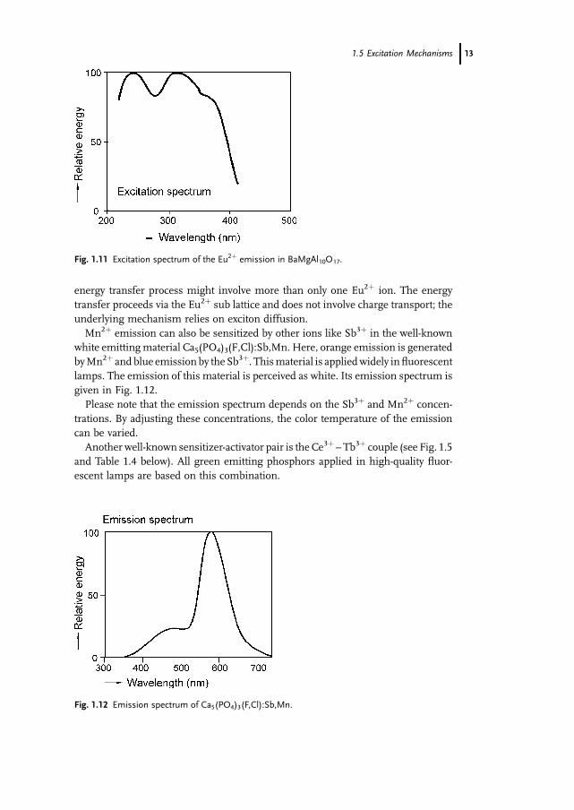
excitation spectrum of BaMgAl10O17:Eu is given in Fig. 1.11.

One observes a strong broad absorption spectrum in theUVpart of the spectrum as

theexcited5dstateof theEu2þ ionissplitby ligandfieldinteractionwiththeoxygenions

surrounding it. In addition, one observes that the absorption extends into the nearUV/

blue part of the optical spectrum; thismakes this material also suitable for application

withnearUVLEDs.Phosphors forLEDsare treated inadedicated chapter in this book.

The excitation spectrum of the Mn2þ spectrum in BaMgAl10O17:Eu,Mn is, in the

UV, very similar to the excitation spectrum of the compound withoutMn2þ. Here we

encounter an example of Eu2þ-sensitized emission of Mn2þ, as proven by the

similarity of the excitation spectrum of both the Eu2þ and the Mn2þ emission.

The very localized excitation (exciton) of Eu2þ is transferred to the Mn2þ ion. The

12 1 Emission and Excitation Mechanisms of Phosphors

energy transfer process might involve more than only one Eu2þ ion. The energy

transfer proceeds via the Eu2þ sub lattice and does not involve charge transport; the

underlying mechanism relies on exciton diffusion.

Mn2þ emission can also be sensitized by other ions like Sb3þ in the well-known

white emittingmaterial Ca5(PO4)3(F,Cl):Sb,Mn. Here, orange emission is generated

byMn2þ and blue emission by the Sb3þ. Thismaterial is appliedwidely in fluorescent

lamps. The emission of this material is perceived as white. Its emission spectrum is

given in Fig. 1.12.

Please note that the emission spectrum depends on the Sb3þ and Mn2þ concen-

trations. By adjusting these concentrations, the color temperature of the emission

can be varied.

Another well-known sensitizer-activator pair is the Ce3þ – Tb3þ couple (see Fig. 1.5

and Table 1.4 below). All green emitting phosphors applied in high-quality fluor-

escent lamps are based on this combination.

Fig. 1.11 Excitation spectrum of the Eu2þ emission in BaMgAl10O17.

Fig. 1.12 Emission spectrum of Ca5(PO4)3(F,Cl):Sb,Mn.

1.5 Excitation Mechanisms 13

1.6

Energy Transfer Mechanisms Between Optical Centers

Energy transfer between a sensitizer ion (S) and an activator ion (A) can bewritten as a

chemical reaction:

S� þ A!Sþ A� ð6Þ

where the asterisk indicates the excited state.

We remark that sensitization can involve even more ions, as in (Ce,Gd,Tb)Mg-

B5O10:Mn (a green and red emitting luminescent material applied in fluorescent

lamps with a very high color rendering), where the energy is transferred from the

Ce3þ ions to the Tb3þ and the Mn2þ ions via the Gd3þ ion sub lattice. The emission

spectrum is given in Fig. 1.13.We observe green Tb3þ emission, redMn2þ emission,

and a trace of Ce3þ emission in the UV, indicating that the energy transfer efficiency

is almost completely unity.

1.6.1

Mechanisms Underlying Energy Transfer

For energy transfer, the sensitizer ion and the activator ion have to show physical

interaction. This energy transfer can find its origin in electrostatic and exchange

interaction. In addition, the emission spectrum of the sensitizer ion and the

absorption spectrum of the activator ion have to show spectral overlap, for energy

conservation reasons.

The probability Wet for energy transfer is given by the following term:

Wet ¼ 2p=�hðrÞ½wijHjwf �2 ð7Þ

Fig. 1.13 Emission spectrum of (Ce,Gd,Tb)(Mg,Mn) B5O10.

14 1 Emission and Excitation Mechanisms of Phosphors

In this term, wi is the wave function of the initial state, wf is the wave function of

the final state, r is a measure for the density of initial and final states capable of

interaction, and H is the operator coupling the initial and final state. r is given

by

r ¼ðgsðEÞgAðEÞdE ð8Þ

representing the spectral overlap between sensitizer and activator ions. gS(E) and

gA(E) are the normalized optical line shape functions for the sensitizer and the

activator ions, respectively.

In this treatment we distinguish between two kinds of interactions: electrostatic

interaction given byHc and exchange interaction described byHe. The probability per

unit time for energy transfer then can be written as

Wet ¼ 2p=�hðrÞf½wðS�ÞwðAÞjHcjwðSÞwðA�Þ�2þ½wðS�ÞwðAÞjHejwðSÞwðA�Þ�2g ð9Þ

Thematrix elements for Coulomb interaction represent the repulsive electrostatic

interaction between the electronic charge distributions in the initial and final state,

respectively, and have the following shape:

QCi ¼ ws� ð1ÞwAð2Þ and QC

f ¼ wsð1ÞwA� ð2Þ ð10Þ

The matrix elements for exchange interaction represent the repulsive electronic

interaction of the electronic charge distributions, and have the following shape:

Qei ¼ ws� ð1ÞwAð2Þ and Qe

f ¼ wsð2ÞwA� ð1Þ ð11Þ

In Fig. 1.14, electronic energy transfer by Coulomb and exchange interaction are

compared. In the case of Coulomb interaction, the electrons initially on the excited

donor stay there, and the electrons initially on the acceptor also remain there. This

interaction does not require physical contact between the interacting partners; it is

sufficient that the excited sensitizer ion induces a dipole oscillation on the activator

ion. In the case of energy transfer governed by exchange interaction, the way the

energy is transferred can be visualized by a double electron substitution reaction: the

excited electron on S� travels to A, whereas one electron on A goes to S. This type of

interaction requires overlap of the electronic charge distribution, i.e. physical contact

between the sensitizer ion and the activator ion.

1.6.2

Energy Transfer Governed by Electrostatic Interaction

In this section, we discuss, using a simple model, the factors governing the

magnitude of the electrostatic interaction and how they relate to the rate of energy

transfer.

1.6 Energy Transfer Mechanisms Between Optical Centers 15

The interaction energy ESA between two dipoles is given by the magnitude of the

two dipoles (mS and mA, respectively) and the distance RSA between them:

ESA /mSmA=R3SA ð12Þ

Forster [1–3] has identifiedmS andmA, respectively, with the oscillator strength for the

radiative transitions S�$ S and A�$A, respectively. We will now treat energy

transfer more quantitatively.

The power irradiated by an oscillating dipole m cosvt is given by

P ¼ 4vjmj2=3c3 ð13Þ

The result obtained is a factor of 4 larger than in classical electrodynamics, to

differentiate between photons absorbed and emitted.

The rate of decay A is given by Eq. (14) (energy emitted per unit time divided by the

photon energy �hv):

A ¼ 1=t0 ¼ ð4vjmj2=ð3c3ÞÞ=ð�hvÞ ð14Þ

in which t0 is the radiative lifetime.

We obtain for jmj2:

jmj2 ¼ 3hc3=ð8pv3t0Þ ð15Þ

Fig. 1.14 Visualization of energy transfer by Coulomb interaction

(a) and exchange interaction (b) between two ions.

16 1 Emission and Excitation Mechanisms of Phosphors

The oscillator strength for an optical transition is related to jmj2 in the following way:

f ¼ 2mvjmj2=ð3�he2Þ ð16Þ

jmj2 is thus given by

jmj2 ¼ ð3�he2Þf=ð2mvÞ ð17Þ

Apart from some numbers we are now able to calculate the rate of energy transfer

from sensitizer ions to activator ions, being the product of equation (14) for the

sensitizer and (17) for the activator ion divided by the distance R6SA

(see above, the

transition rate contains the matrix element for the energy squared):

WSA / 3hc3=ð8pv3t0SÞð3�he2ÞfA=ð2mvR6SAÞ ð18Þ

Or, after some rearrangements and inclusion of the numbers mentioned above

(which partly originate from the expansion of the interaction Hamiltonian in

spherical harmonics), the following equation is obtained [4]:

WSA ¼ 2p=�h=R6SA

� 3e2c3�h6=4m � fA=tS �h �

ðgSðEÞgAðEÞ=E4dE ð19Þ

In this equation, tS is the decay time of the sensitizer ion and h is the quantum

efficiency of the sensitizer ion.

Equation (19) can also be written as:

WSA ¼ 1=tS � ðR0=RSAÞ6 ð20Þ

where R0 is the distance at which the transfer rate to the activator is equal to the decay

rate of the sensitizer and is given by:

R60 ¼ hfAð3e2c3�h5p=2mÞ

ðgSðEÞgAðEÞ=E4

�dE ð21Þ

Inspection of the equations derived shows that energy transfer, governed by

Coulomb interaction, is favored by a large spectral overlap, a small value of the

intrinsic decay time of the sensitizer ion, a large absorption strength of the activator

ion, and a small distance between the sensitizer and activator ion.

In practice, it is of more importance to determine the efficiency of the energy

transfer process than the rate.

The decay of the sensitizer ion is given by:

1=tS ¼ 1=t0 þ 1=tS �R60=R

6SA ð22Þ

The yield hSA for energy transfer is therefore given by:

�SA ¼ 1=�S �R60=R

6SA=ð1=�SÞ ð23Þ

1.6 Energy Transfer Mechanisms Between Optical Centers 17

the energy transferred per unit time divided by the total amount of energy emitted per

unit time.

For the efficiency of the energy transfer process hSA, we therefore find the

following proportionality :

hSA ¼ ðR0=RSAÞ6 ð24Þ

Please note that the quantum efficiency of the sensitizer ion is contained in R0 [see

Eq. (21)]. For a distance RSA between the sensitizer ion and the activator ion smaller

than R0, energy transfer will dominate; in the opposite case, inherent decay of the

sensitising ion S� is the most important process. Moreover, though the energy

transfer rate increases with decreasing tS, the same applies to the sensitizer emission

probability. Therefore, the transfer yield is independent of tS.

1.6.3

Energy Transfer by Higher-order Coulomb Interaction

Apart from dipolar interaction, higher-order interaction may also result in energy

transfer. In Table 1.1, the distance dependence of interaction involving dipoles and

quadrupoles is summarized for the case that the optical transitions involved are spin

allowed:

A more quantitative analysis, using the expressions derived above, shows that in

the case of electric dipole interaction:� Energy transfer from a broad-band emitter to a line absorber

only occurs between nearest neighbors.� Energy transfer from a line emitter to a broad-band absorber is

possible for distances up to about 2 nm.� Energy transfer from a broad-band emitter to a broad-band

absorber is possible for distances as large as about 3.5 nm.� Dipole-dipole interactions and dipole-quadrupole interactions

can result in energy transfer in solids: both interactions can

take place over metal ion–metal ion distances which are

observed in solids.� Interactions between electric quadrupoles are not expected to

play an important role in solids in view of the very short

interaction range.

Tab. 1.1 Equations for energy transfer governed by Coulomb

interaction as a function of the type of interaction for spin-

allowed transitions.

Interaction type Equation form Range (nm)

Electric dipole – electric dipole WSA = (1/tS) (R0/RSA)6 3.5

Electric dipole – electric quadrupole WSA = (1/tS) (R0/RSA)8 0.8

Electric quadrupole – electric quadrupole WSA = (1/tS) (R0/RSA)10 0.2

18 1 Emission and Excitation Mechanisms of Phosphors

1.6.4

Energy Transfer Governed by Exchange Interactions

Dexter has formulated a theory describing energy transfer by exchange interaction [5].

The rate constant for energy transfer is written as

WSA ¼ K J expð�2RSA=LÞ ð25Þ

In equation (25), K is a constant determined by the interaction between the orbitals

involved in the energy transfer process, J is determined by the spectral overlap

integral, normalized for the absorption strength of the activator ion, and L is

determined by the van der Waals radii of the interacting ions. The exponential

dependence is due to the fact that the electron density in general falls off exponen-

tially with the distance between the electron and the nucleus.

As the energy transfer process does not involve electric dipole interaction, no

dependence of the magnitude of the electric dipoles on the sensitizer and activator

ions is expected. In view of the relationship between the magnitude of the electric

dipoles and the oscillator strength (see above), therefore, no relation between the

oscillator strength of the optical transitions on sensitizer and activator ion is

expected. In fact, for exchange interaction, there is no relation between the

interaction between the ions and any spectroscopic characteristic of the sensitizer

or activator ions.

Another difference between energy transfer governed by Coulomb and exchange

interaction is the distance dependence. The rate of energy transfer shows an R�nSA

dependence in the case of Coulomb interaction and an exp(�RSA/L) dependence in

the case of energy transfer by exchange interaction. In the case of energy transfer by

exchange interaction, the rate drops very quickly for distances RSA greater than about

1 nm.

Finally, exchange interaction, due to the requirement of wave function overlap, has

a pronounced angular dependency and is also dependent on covalence.

1.6.5

Cross-relaxation and Energy Transfer

Aphenomenon not discussed until now is cross-relaxation. In such a process, which

can also be looked upon as energy transfer, the excited ion transfers only part of its

energy to another ion. For two Tb3þ ions, the process is depicted in Fig. 1.15. In this

case, the energy difference between the 5D3 and5D4 excited states matches approxi-

mately the energy difference between the 7F6 ground state and higher7FJ states. As in

the energy transfer processes discussed above, at large Tb-Tb distances, the process

of cross-relaxation has a low rate. In many host lattices, therefore, at low Tb

concentration, emission from both the 5D3 and5D4 excited states is observed (unless

the gap between these two states is bridged by phonon emission, for which relatively

high-energy phonons are required, which is, for example, the case with InBO3:Tb).

The resulting emission spectrum has emission from the near UV into the red part of

1.6 Energy Transfer Mechanisms Between Optical Centers 19

the optical spectrum.At higher Tb concentrations (in the order of five percent), cross-

relaxation quenches the emission from the 5D3 level in favor of emission originating

from the 5D4 level, implying that it is not possible to obtain blue Tb3þ emission in

luminescent materials with higher Tb3þ concentrations.

Cross-relaxation also occurs for other ions. It quenches blue Eu3þ emission even at

relatively lowEu3þ concentrations (<1%) in favor of thewell-known red emission. In

case of ions like Sm3þ and Dy3þ, cross-relaxation leads to quenching of the visible

emission. This seriously limits the applicability of these ions.

1.6.6

Practical Implications

Of course, the arguments developed above have practical implications. In general, the

activator ions used in luminescent materials are rather expensive. This implies that

the concentration of the activator ions should be as low as possible. When energy

transfer processes are important, the smallest activator concentrations are possible

for the case of broadband-emitting sensitizers and broadband-absorbing activators.

On the other hand, for high-quality fluorescent lamps, line emitters are required to

obtain an optimized adaptation of the emission spectrum to the human eye with

respect to the amount of visible light generated and the need to reproduce all colors in

a natural way. As discussed above, this requires that sensitizer ion and activator ion

are nearest neighbors, i.e. at least one of the two kinds of ions should be present in

relatively high concentrations.

Fig. 1.15 Cross-relaxation between two Tb3þ ions.

20 1 Emission and Excitation Mechanisms of Phosphors

When optical absorption on the activator ions is forbidden at the energy where the

sensitizer ion emits (the activator ions, however, should have an excited state there),

in principle there are nevertheless two options to obtain energy transfer:� Coulomb interaction exploiting the quadrupole of the activator

ion. This is the mechanism underlying the fluorescent

lampphosphorsBaMgAl10O17:Eu,Mn[6] and (Ce,Tb)MgAl11O19

[7].Because of the vanishingly small spectral overlapbetween the

Ce3þ absorption and the emission bands, no energy migration

between the Ce ions takes place. This requires not only short

Ce-Tb distances in this luminescent material, but also relatively

high Tb concentrations, to prevent Ce emission from occurring.� Exchange interaction between sensitizer and activator ion. As

shown above, this mechanism does not require allowed optical

transitions. This is the mechanism which is operative in the

one-component white fluorescent lamp phosphor

Ca5(PO4)3(F,Cl):Sb,Mn, as deduced from an analysis of the

decay curve for someMn2þ concentrations [8]. The same study

did not reveal evidence for energy transfer between antimony

ions, indicating the necessity of nearest neighbor Sb-Mn

interaction, which is a prerequisite for energy transfer via

exchange interaction. Please note, in addition, that in view of

the large Stokes shift between absorption and emission on the

Sb3þ ion in this lattice, no energy transfer between the anti-

mony ions is expected.

Both for electric dipole – electric quadrupole and exchange interaction, the

distance between sensitizer ion and activator ion has to be rather small, not larger

than about 1 nm. This requires high activator and/or sensitizer ion concentrations,

which is a disadvantage, considering the high costs of these materials.

1.7

Excitation with High-energy Particles

After absorption of electrons or high-energy photons (e.g., X-ray quanta) impinging

on the phosphormaterial, primary electrons and holes in very deep shells are created.

Whereas the holes are tightly bound, the electrons can move in the lattice (and a

fraction of the electrons generated can leave the material). The primary ionization

event is followed by radiative decay (secondary X-rays, the basis for EDAX), non-

radiative decay (the generation of secondary electrons by Auger processes), and

inelastic electron-electron scattering. These processes are very fast and occur typically

in the 10�15–10�13 s regime after the primary absorption. During these processes,

many electrons are excited.

When the energy of the electrons generated is lower than the ionization threshold,

the hot electrons and holes thermalize by intraband transitions and electron-optical

1.7 Excitation with High-energy Particles 21

phonon interaction. Also during this process, activator or sensitizer ions may be

excited by impact excitation by hot electrons, by sequential excitation by capture of

mobile charge carriers (electrons and holes), and by excitons. These processes

typically occur in a time frame 10�12–10�8 s and may therefore lead to a clearly

visible rise time of the emission.

In the last step, luminescence can occur in a time frame of 10�9 s for very fast

allowed optical transitions up to ms or even longer times for forbidden transitions.

Robbins has treated these processesmore quantitatively [9]. In this chapter, we only

outline this excellent treatment. Themore interested reader is referred to the original

paper.

The energy efficiency of the overall process is given by

h ¼ ð1� rÞ½hn�=ðbEgÞ �hthacthesc ð26Þ

in which r is the backscatter coefficient, expressing the fact that not all high-energy

particles enter the material, [hn] is the mean photon energy of the photons emitted,

bEg the energy needed to generate a thermalized electron-hole pair (b being a pure

number and Eg being the band gap energy), ht is the transfer efficiency of electron-

hole pairs to activators or sensitizers, hact is the quantum efficiency of the activator

ions (whichgives the ratio of thenumber of photons emitteddividedby thenumber of

photons absorbed), and finally hesc is the ratio between photons leaving the material

and photons generated in the material (escape probability).

Backscattering is negligible for X-rays, whereas for electrons the backscatter

coefficient r generally has values between 0.1 and 0.2.

For applications, phosphors operating at physical limits are of interest only. This

means that the transfer efficiency, the activator efficiency, and the escape probability

have to be unity. Equation (26) then simplifies to

h ¼ ð1� rÞ½hn�=bEg ð27Þ

Inspection of this equation shows that the energy efficiency is determined by the

mean energy of the photons emitted by the activator ions and by the productbEg. The

primary particles, eventually generating the luminescence, lose their energy by

impact ionization and generation of optical phonons. In what follows, we discuss

thismechanism in somemore detail. It is important to note that the description boils

down to calculating what fraction of the energy that impinges on thematerial is used

to create electron-hole pairs with energy (almost) equal to the band gap energy. The

energymight be slightly smaller than thebandgap energy, as the electron and thehole

can attract each other by Coulomb interaction. In such a case an exciton is formed.

Further, the reader should carefully note that this treatment gives the maximum

efficiencies only.

InChapter 5,which dealswith scintillatingmaterials, wewill use expression (27) in

a slightly different form. In scintillator physics, the light yield is generally expressed

in the units [photons/MeV of excitation energy]. Scintillating materials can generate

more than 70 000 photons per MeV of excitation energy. For scintillators, the light

22 1 Emission and Excitation Mechanisms of Phosphors

yield ismore useful than the energy efficiency in viewof the fact that photons are to be

detected.

The average energy needed to create an electron-hole pair can be written as

bEg ¼ Ei þ Eop þ 2Ef ð28Þ

In this expression, Ei is the ionization threshold, Eop the average energy lost in

generating optical phonons, and Ef is the threshold energy for the generation of

electron-hole pairs.

The ratio of the energy needed to generate optical phonons with frequency �hvLO

and impact ionization is proportional to R, which in turn is given by

R ¼ ð1=e1 � 1=eoÞð�hvLOÞ1:5=ð1:5 EgÞ ð29Þ

in which e1 and eo are the optical and static dielectric constants of the phosphor

host lattice, respectively. The dependence of b on R is given in Fig. 1.16, in which a

slightly different notation for the expression dealing with the dielectric constants is

used.

The value of b is found to vary between about 2.5 and 10 for a number of host

lattices. We observe that in order to obtain host lattices with small b, resulting in

highly efficient phosphors, the value of R should be small as well. This condition

implies a low optical phonon frequency or a small difference between the optical and

the static dielectric constant. In Table 1.2, the relevant data are given for a number of

well-known phosphor materials. We observe a good agreement between the energy

efficiencies observed and the maximum efficiencies predicted.

Please note that this treatment deals with host lattice properties only, i.e. it is the

host lattice properties which decide whether the impinging energy is efficiently

converted into energy gap excitations. This is in line with observations: quite a few

host lattices show efficient cathode rays from X-ray excited luminescence when

doped with different activators. Examples are ZnS, CaS (see Table 1.2) and the rare

Fig. 1.16 Dependence of b on R.

1.7 Excitation with High-energy Particles 23

Tab. 1.2 Physical constants of a number of efficient host

lattice-excited phosphors. hthe is the maximum efficiency

calculated, hexp is the energy efficiency observed experimentally.

Phosphor �hvLO (eV) Eg (eV ) [hn] (eV) b hthe hexp

CsI:Tl 0.011 6.4 2.25 2.5 0.14 0.14

ZnS:Ag 0.044 3.8 2.75 2.9 0.25 0.20

ZnS:Cu 0.044 3.8 2.3 2.9 0.21 0.17

CaS:Ce 0.047 4.8 2.3 3.0 0.16 0.22

CaS:Mn 0.047 4.8 2.1 3.0 0.15 0.16

La2O2S:Eu 0.057 4.4 2.0 3.9 0.12 0.11

Y2O3:Eu 0.068 5.6 2.0 4.6 0.07 0.08

YVO4:Eu 0.116 3.7 2.0 7.5 0.07 0.07

earth oxysulfides (like Gd2O2S, which shows efficient emission when doped with

Pr3þ, Eu3þ or Tb3þ).

The mechanism discussed above involves efficient energy transfer from host

lattice states to localized states. This mechanism also occurs in some luminescent

materials applied inXe-discharges. TheXe-discharge generates radiation in the VUV

part of the spectrum. In these materials, the host lattice itself acts as sensitizer.

We remark that an alternative description for the generation of electron-hole pair

generation has been formulated [10]. In this model, b can be much smaller than the

values derived by Robbins (close to unity and virtually material independent). In this

model, transfer from host to activator ions is the energy efficiency determining step.

Interesting feature of this model is that also ionic materials could have very high

photon yields.

1.8

Electroluminescence (EL)

1.8.1

High-voltage Electroluminescence

High-voltage electroluminescence relies on an electrical breakthrough in a semi-

conducting material, which rationalizes the necessity to use rather high voltages.

Generally speaking, the lifetime of such electroluminescent devices can be long but

the efficiencies are rather low (in the order of one percent, see below) and conse-

quently applications are found in segmentswhere reliability is an issue and efficiency

considerations are not very important (emergency signs, exit signs, and interestingly

ceiling illumination in the Maybach premium car). Prominent materials are

ZnS:Mn, ZnS:Cu, and SrS:Ce, although oxides are under investigation as well.

The luminescentmaterials areused in thin layers (in theorderof1mm)generatedby

techniques like atomic- ormolecular beamepitaxy, althoughpowder EL is also known.

Thematerials are subjected to high electric fields, and electrons are accelerated in the

materials.Theelectronsexcitetheactivatorionsbyimpactexcitation.Atpresent, thereis

no general picture of themechanism(s) underlyinghigh-voltage electroluminescence.

24 1 Emission and Excitation Mechanisms of Phosphors

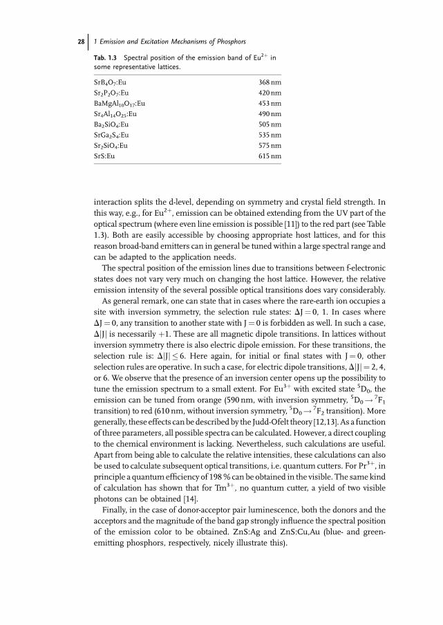
We will give a very elementary treatment, which yields the energy efficiency to be

expected, without considering the mechanism(s) in detail.

The maximum efficiency h is given by:

h ¼ EemsN=eF ð30Þ

in which Eem is the photon energy of the emitted radiation, s the cross-section for

impact excitation, N the optimum concentration of luminescent centers, and F the

electric field applied. Dimensional analysis shows that (sN)�1 has the units [m]. The

physical meaning of (sN)�1 is the mean distance that an electron travels through

the luminescent material between two excitation events.

The cross-section is not known a priori. In the case of ZnS:Mn (the most efficient

ACTFEL material known), we approximate it by using atomic dimensions, i.e.

s¼ 10�16 cm2 (the Mn2þ ions has the same charge and approximately the same

size as the Zn2þ ion). The other typical values are: Eem¼ 2 eV, N¼ 1020 cm�3 and

F¼ 106 Vcm�1. It follows that the energy efficiency equals about 2%,which is in very

good agreementwith experiment. In this treatment, however, wehave used anumber

of simplifications. We did not account for the Stokes shift. Moreover, we neglected

light-trapping effects in the thin layers. All these phenomena further reduce the

energy efficiency. However, the energy efficiency is not likely to be improved

significantly. This is mainly because of the low value for the cross-section, because

N cannot be chosen to be too large in view of concentration quenching.

The mean energy that the charge carrier has taken up from the electric field

between two impact excitation events equals eF/sN, neglecting any losses due to

phonon emission. The minimum pathway that an electron has to travel to be able to

excite an activator ion Lcrit equals Lcrit¼Eexc/eF, where Eexc is the energy needed for

the excitation of the luminescence. Please note that Lcrit is dependent on the electric

field strength. Incorporation of Lcrit in Eq. (30) yields

h ¼ Eem=Eexc �sN �Lcrit ð31Þ

In the case of excitation of luminescence via host-lattice states (see above), the

luminescence efficiency can be written very generally as

h ¼ Eem=Eexc �ht �hact �hesc ð32Þ

In this expressionht is the probability of energy transfer from the host lattice to the

activator ions, hact is the quantum efficiency of the activator, and finally hesc is the

escape probability – the ratio between thenumber of photons leaving thematerial and

the number of photons generated in the material. On assuming hact and hesc to be

unity, the maximum energy efficiency for the ACTFEL process is given by:

h ¼ Eem=Eexc �ht ð33Þ

Inspection of Eqs. (31) and (33) leads to the conclusion that sN �Lcrit is the transfer

efficiency. In case of cathode ray excitation, this figure can be unity. In case of

1.8 Electroluminescence (EL) 25

ZnS:Mn, its optimal value is calculated to be about 0.02 only. The low transfer

efficiency of energy from host lattice states to activator states is the main reason for

the low energy efficiency of this material, but still it is the most efficient one known!

Please note that this equation shows that themaximum efficiency of EL phosphors is

determined by both host-lattice and dopant properties.

1.8.2

Low-voltage Electroluminescence

The advent of the blue light-emitting diode (LED) and of organic electroluminescent

structures has strongly revitalized interest in this luminescence mechanism. For the

first time, efficient light-emitting structures can be realized which do not require

either high or low pressure. In addition, luminescent devices have always hitherto

used a cascade – in fluorescent lamps, first a discharge is generated and the resulting

invisible radiation is converted into visible light, resulting in a (considerable) energy

loss. In cathode ray tubes, first an electron beam consisting of electrons with rather

high kinetic energy is generated, which subsequently impinges on the luminescent

material. In the phosphors, electron bombardment finally leads to excitations where

electrons in the conduction band are coupled to holes in the valence band (excitons).

These excitons are transferred to activator ions. As a result, there are no white light-

emitting devices with energy efficiency greater than 50%. Low-voltage electrolumi-

nescent devicesmight be away out here. In such devices, the step leading to emission

is the recombination of electrons in conduction band states with holes in valence

band states, and in principle only the band gap energy is required to excite the

luminescence. Within limits, the color of the emission can be selected by choosing

the appropriate semiconductor. The generation of luminescence can be very energy

efficient; the main issue is getting the light out of the emitting device. LEDs are

available with wall plug efficiency approaching 70%.

Apart fromefficiency, the power dissipated by LEDs is also an important driver, as it

contributes to the light output that such a device can generate. Lighting applications

generally require a light output of 1Wand above. LEDs with input power of 30Wand

external energy efficiency of about 10% have been demonstrated by the Japanese

company Nichia and Philips Lumileds.

In this book, luminescent materials that can be used in inorganic low-voltage

electroluminescent devices are discussed in a separate chapter. Phosphors are used

for two reasons:� Inorganic LEDs generally generate narrow line emission.

Combination of LEDs emitting in different spectra regions to

generate white light therefore results in white light of low

quality: it cannot reproduce all colors in a natural way.� Efficient LEDs are not yet available in all colors required.

Especially green is a concern.

Phosphors for LEDs have to fulfill rather harsh conditions. The Stokes shift must

be small, the absorptionmust be high, and, in addition, as the excitation densities are

26 1 Emission and Excitation Mechanisms of Phosphors

in the order of 20Wcm�2 (the area which emits light is much smaller than, e.g., in

fluorescent lamps), the luminescent materials must remain efficient up to high

temperatures, should not show saturation (meaning a less than linear increase in

output power with input power at high excitation densities), and must be radiation

stable.

1.9

Factors Determining the Emission Color

Many luminescent ions show emission at different wavelengths in different host

lattices. This phenomenon, once understood, opens up the possibility to change,

within certain limits, the emission color. In this way, the emission spectra (and

excitation spectra) can be tuned toward the specifications required.

In cases where at least one of the electronic states is involved in the chemical

bonding, the coupling to the lattice has to be taken into account. This situation is

encountered for many transition metal ions, for the s2 ions, and for rare-earth ions

showing d! f emission.

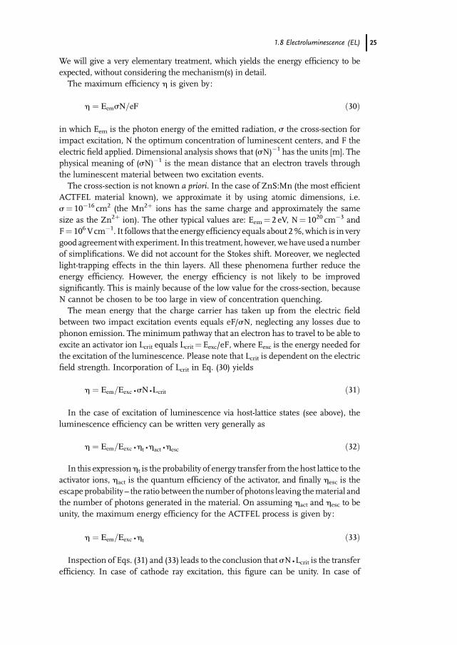
In Fig. 1.17, this situation is illustrated for d! f optical transition on Eu2þ.

Other rare-earth ions showing d! f emission are Ce3þ, Pr3þ, Nd3þ and Er3þ,

albeit for the last three ions only in the UV.

The energy difference between the d- and f-electrons is modified by the covalence

of the Eu2þ-ligand bond and the crystal field strength. An increase of the covalence of

the Eu2þ-ligand bond results in a lower energy difference of the 4f-5d energy

separation (due to the nephelauxetic effect). This elementary treatment considers

the shift of the center of gravity (also called barycenter) of the d-electron level (also

called centroid shift), i.e. any splitting is not yet taken into account. The crystal field

Fig. 1.17 Energy separation of the 4f7 and 4f65d1 bands as a function of

covalence and ligand field strength. The arrows indicate different emission

colors.

1.9 Factors Determining the Emission Color 27

interaction splits the d-level, depending on symmetry and crystal field strength. In

this way, e.g., for Eu2þ, emission can be obtained extending from the UV part of the

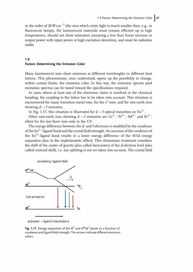
optical spectrum (where even line emission is possible [11]) to the red part (see Table

1.3). Both are easily accessible by choosing appropriate host lattices, and for this

reason broad-band emitters can in general be tuned within a large spectral range and

can be adapted to the application needs.

The spectral position of the emission lines due to transitions between f-electronic

states does not vary very much on changing the host lattice. However, the relative

emission intensity of the several possible optical transitions does vary considerably.

As general remark, one can state that in cases where the rare-earth ion occupies a

site with inversion symmetry, the selection rule states: DJ¼ 0, 1. In cases where

DJ¼ 0, any transition to another state with J¼ 0 is forbidden as well. In such a case,

DjJj is necessarily þ1. These are all magnetic dipole transitions. In lattices without

inversion symmetry there is also electric dipole emission. For these transitions, the

selection rule is: DjJj � 6. Here again, for initial or final states with J¼ 0, other

selection rules are operative. In such a case, for electric dipole transitions,DjJj ¼ 2, 4,

or 6. We observe that the presence of an inversion center opens up the possibility to

tune the emission spectrum to a small extent. For Eu3þ with excited state 5D0, the

emission can be tuned from orange (590 nm, with inversion symmetry, 5D0! 7F1transition) to red (610 nm, without inversion symmetry, 5D0! 7F2 transition). More

generally, these effects canbe describedby the Judd-Ofelt theory [12,13]. As a function

of three parameters, all possible spectra can be calculated. However, a direct coupling

to the chemical environment is lacking. Nevertheless, such calculations are useful.

Apart from being able to calculate the relative intensities, these calculations can also

be used to calculate subsequent optical transitions, i.e. quantum cutters. For Pr3þ, in

principle a quantumefficiency of 198% can be obtained in the visible. The same kind

of calculation has shown that for Tm3þ, no quantum cutter, a yield of two visible

photons can be obtained [14].

Finally, in the case of donor-acceptor pair luminescence, both the donors and the

acceptors and themagnitude of the band gap strongly influence the spectral position

of the emission color to be obtained. ZnS:Ag and ZnS:Cu,Au (blue- and green-

emitting phosphors, respectively, nicely illustrate this).

Tab. 1.3 Spectral position of the emission band of Eu2þ in

some representative lattices.

SrB4O7:Eu 368 nm

Sr2P2O7:Eu 420 nm

BaMgAl10O17:Eu 453 nm

Sr4Al14O25:Eu 490 nm

Ba2SiO4:Eu 505 nm

SrGa2S4:Eu 535 nm

Sr2SiO4:Eu 575 nm

SrS:Eu 615 nm

28 1 Emission and Excitation Mechanisms of Phosphors

1.10

Energy Efficiency Considerations of Important Luminescent Devices

As argued above, in general, the luminescent materials applied operate at physical

limits in terms of absorption of the exciting radiation and the quantum efficiency

(number of visible photons generated divided by the number of photons absorbed)

with which luminescence is generated. In cathode ray tubes, the energy efficiency of

the phosphors used is at maximum (up to about 25%, see above), and the quantum

efficiency of the luminescent centers is almost 100%.

In plasma display panels, fluorescent lamps, and LEDs, the quantum efficiency

amounts about 100%, and the absorption coefficient is also very high. Nevertheless,

the energy efficiency of luminescent devices is rather low (see Table 1.4) in which the

energy loss in factorized. The phosphor energy loss factor in this table is mainly

determined by the Stokes shift (the difference in photon energy of radiation absorbed

and emitted). This results in energy loss, which can be significant even when the

quantum efficiency is 100%.

We observe that, although the phosphors operate at physical limits, nevertheless

the energy efficiency of the devices is rather low, especially in display applications.

Finally, Table 1.5 gives a survey of luminescentmaterials with popular applications.

1.11

Luminescence Quantum Yield and Quenching Processes

In this section, we deal with energy loss processes, to throw some light on the question

whyallphosphorsdonothaveaquantumefficiencyofunityandwhat the lossprocesses

are.We base this discussion on Eq. (26).We also briefly discuss degradation processes

in luminescentmaterials,which quite frequently occur during the operation of devices

utilizing phosphors and which have a negative effect on the performance of such

devices. The influenceondevice performance canbe considerable, especially in case of

Tab. 1.4 Energy efficiencies of important luminescent devices

and a breakdown into the most important energy loss factors.

Device Cathode

ray tube

Plasma

display panel

Fluorescent

lamp

Phosphor-converted

LED lamp

Energy

efficiency (%)

1–2 2 Straight

fluorescent: 25

50

Compact: 15

Major energy

loss factors (%)

Shadow

mask: 70–90

Discharge: 90

Phosphors: 70

Phosphors: 55

Discharge: 30

LED: 40

Phosphors: 25

Phosphors: 80 (Straight)

Deflection yoke: 50 Discharge: 40

(Compact)

1.11 Luminescence Quantum Yield and Quenching Processes 29

Tab.1.5

Prominen

tphosphors

andtheirap

plications.

Emission

color

Application

Cathoderaytubes

andprojection

televisiontubes

(PTV)

Plasm

adisplay

pan

els

Fluorescentlamps

X-ray

detectors

LEDs

UV

Ba 2SiO

5:Pb2þ(suntanning)

CeM

gAl 11O19(suntanning)

LaP

O4:Ce3

þ(suntanning)

SrB

4O7:Eu2þ(suntanning,

photocopiers)

Blue

ZnS:Ag+,Cl�

ZnS:Ag+,Al3þ

BaM

gAl 10O17:Eu2þ

BaM

gAl 10O17:Eu2þ

NaI:Tl+

Sr 4Al 14O25:Eu2þ

Ba(F,Br):Eu2þ

Sr 5(PO4) 3Cl:Eu2þ

(storagephosphor)

LaB

r 3:Ce3

þ

Bi 4Ge 3O12

Gd2SiO

5:Ce3

þ

Lu2SiO

5:Ce3

þ

LuAlO

3:Ce3

þ

YTaO4:Nb5þ

Green

ZnS:Cu+,Au+,Al3þ

(Y,Gd)BO3:Tb

GdMgB5O10:Ce3

þ,Tb3þ

CsI:Tl+

ZnS:Cu+,Al3þ

BaA

l 12O19:M

n2þ

LaP

O4:Ce3

þ,Tb3þ

Gd2O2S:Tb3þ

Zn2SiO

4:M

n2þ(PTV)

Zn2SiO

4:M

n2þ

CeM

gAl 11O19:Tb3þ

Gd2O2S:Pr3þ

Y2SiO

5:Tb3þ(PTV)

BaM

gAl 10O17:Eu2þ,M

n2þ

Zn2SiO

4:M

n2þ

InBO3:Tb3þ(PTV)

LaO

Cl:Tb3þ(PTV)

Yellow

Y3Al 5O12:Ce3

þ(Y,Gd) 3Al 5O12:Ce3

þ

Red

Y2O2S:Eu3þ

Y2O3:Eu3

Y2O3:Eu3þ

(Y,Gd) 2O3:Eu3þ,Pr3

þCaS:Eu

Y2O3:Eu(PTV)

(Y,Gd)(P,V)O

4:Eu3þ

White

ZnS:Ag++(Zn,Cd)S:Ag+

Ca 5(PO4) 3(F,Cl):Sb3þ,M

n2þ

cathode ray tubes, where phosphor degradation can contribute to an efficiency loss up

to 30–50% during the operational lifetime. In fluorescent lamps, the maintenance of

the phosphors is in general much better, and the efficiency loss over the operational

lifetime can be less than 10%.

Looking at the expression in Eq. (26), we distinguish the following loss processes:

1. The absorbed energy does not reach the luminescent ions (ht).

2. The absorbed energy reaches the luminescent ions but there

are nonradiative channels to the ground state (hact).

3. The luminescence generated is absorbed by the luminescent

material (hesc).

In what follows, the underlying mechanisms will be treated in more detail.

1.11.1

The Energy does not Reach the Luminescent Ion

When there ismore than one origin of optical absorption at thewavelength at which

the excitation takes place, the quantum efficiency can be less than unity, even if the

ion showing luminescence has a quantum efficiency of one. This is, e.g., the case if

both the luminescent ion and the host lattice show optical absorption at the

excitation wavelength, or the energy transfer probability of the host lattice to the

luminescent ions is smaller than unity. Comparing the absorption or reflection

spectra with the excitation spectra can disentangle the different contributions to the

absorption.

Degradation of luminescent materials can be due to creation of additional absorp-

tion centers in the spectral range where the activators or sensitizers also absorb.

1.11.2

The Absorbed Energy Reaches the Luminescent Ion but there are Nonradiative

Channels to the Ground State

The transition rate (units s�1) is given by k. If only emission occurs, k is written as kr.

If the transition involves radiative and nonradiative contributions, k is written as

k ¼ kr þ knr ð34Þ

We observe that k increases in the case of nonradiative contributions to the

transition rate. For this reason, the emission decay time (being 1/k) decreases in such

cases. Using this expression, it is easily shown that the quantum yield can be

determined by measuring the decay time (t) if the decay time without nonradiative

transitions (to) is known:

QE ¼ t=to ð35Þ

The proof of this equation is left to the reader.

1.11 Luminescence Quantum Yield and Quenching Processes 31

Very frequently, the luminescent ion can reach the ground state via thermal

quenching (see Fig. 1.18). This is the case when the excited state and the ground

state energy curves cross at an energy which is thermally accessible from the

relaxed excited state. For this reason, this process is called thermal quenching.

Using the rate equations again, and assuming that the nonradiative rate knr can be

written as

knr ¼ A �expð�E=kTÞ ð36Þ

inwhichA is a constant (units s�1) andE is the energy difference between the energy

of the relaxed excited state and the energy at which the ground and excited states

cross (Fig. 1.18).

The quantum efficiency is given by

QE ¼ 1=ð1þ C �expð�E=kTÞÞ ð37Þ

in which C is a dimensionless constant.

We observe that an increase in temperature results in a lower value for the

quantum efficiency. The energy involved in the thermal quenching process is easily

determined by measuring the decay time of quantum efficiency as a function of the

temperature.

Of course, the elementary treatment leading to Eq. (37) describes quenching due to

any thermally activated process, e.g., also thermal quenching due to photoionization.

In this process, excited activator ions ionize thermally activated . This process is very

important in, e.g., scintillators.

Another quenching process is related to energy transfer. If the concentration of

luminescent ions chosen is too high, energy transfer occurs over the luminescent

Fig. 1.18 Crossing of parabolas describing ground and excited states,

leading to thermal quenching characterized by the activation energy E.

32 1 Emission and Excitation Mechanisms of Phosphors

ions until the energy reaches a center where a nonradiative transition occurs. Two

remarks have to be made here:� Energy transfer underlies sensitization schemes, in which case

energy transfer is a useful process. Though the sensitizer

emission is quenched, the activator emission appears. This

allows practical application of sensitization schemes.� In general the centers for nonradiative recombination are not

known. Inmany cases, therefore, the possibility to increase the

concentration of luminescent ions is limited. The mechanism

leading to quantum yield loss is called concentration

quenching. Whether or not this mechanism takes place can be

easily deduced by investigating the quantum efficiency or the

decay time of the emission as a function of the activator

concentration.

Please note that a large difference between absorption and emission wavelength

(Stokes shift) reduces energy transfer and therefore concentration quenching.On the

other hand, a very large Stokes shift increases the probability for thermal quenching,

as the ground state parabola will cross the excited state parabola at a lower energy,

allowing the ground state parabola to be reached without emission of a photon. This

is a direct consequence of the quadratic dependence of the potential energy of the

electronic states on the metal-ligand distance, as the reader can easily verify. For the

same reason, thermal quenching becomes less probable when the emission energy

increases.

Degradation of luminescent materials can be due to additional centers to which

energy can be transferred, without efficient photon generation by these centers

(killing centers, killers, centers for nonradiative recombination). Such centers can be,

e.g., vacancies generated as a consequence of the operation of the device or sensitizer

or activator ions that have changed their valence during operation of the device.

1.11.3

The Luminescence Generated is Absorbed by the Luminescent Material

Finally, even if all the absorbed energy is converted into emission, the quantum

efficiency isnot necessarily one. For example, this is the casewhen thehost lattice itself

shows optical absorption in the spectral range where emission occurs. This is easily

determined by measuring the absorption or reflection spectra of the host material.

Self-absorption is also an important loss factor in luminescent structures which do

not effectively scatter the luminescence light. This is the case, e.g., in organic or

inorganic LEDs, where trapping of light in the luminescent structure, followed by

absorption of the light emitted in the luminescentmaterial, strongly reduces the light

output. In such a case, additional scattering, e.g., by applying scattering layers to such

structures or applying photonic structures such that light is generated in desired

directions only, can be a way out.

1.11 Luminescence Quantum Yield and Quenching Processes 33

Degradation of luminescent materials (resulting in a loss of photon generating

efficiency) is often due to additional absorption bands which are not present in the

virgin material. Absorption or reflection spectroscopy therefore are important

techniques in understanding the physical origin of light generation losses of

phosphors.

1.12

Acknowledgement

Considerable parts of the contents of this chapter (text and figures) have appeared in

Refs. [15–17]. With kind permission of Springer Science and Business Media and

World Scientific.

References

1 Forster, T. (1951) FluoreszenzOrganischer Verbindungen,Vandenhoech, Ruprech, Gottingen.

2 Forster, T. (1959) Disc. Faraday Soc.,27, 7.

3 Forster, T. Ann. Phys., (1948) 2, 55.4 DiBartolo, B. (1984) Energy Transfer

Processes in Condensed Matter, in

NATO ASI Series, Series B: Physics, (ed.B. DiBartolo) 114, Plenum Press, New

York.

5 Dexter, D. L. (1953) J. Chem. Phys., 21,836.

6 Stevels, A. L. N. and Verstegen, J. M.

P. J. (1976) J. Lumin., 14, 207.7 Verstegen, J. M. P. J., Sommerdijk, J.

L., Verriet, J. G. (1973) J. Lumin., 6,425.

8 Soules, T. F., Bateman, R.L., Hewes,

R. L., Kreidler, E. R. (1973) Phys. Rev.,B7, 1657.

9 Robbins, D. J. (1980) J. Electrochem.Soc., 127, 2694.

10 Bartram, R. H., Lempicki, A. (1996)

J. Lumin., 69, 225.

11 Meijerink, A., Nuyten, J., Blasse, G.

(1989) J. Lum., 44, 19.12 Ofelt, G. S. (1962) J. Chem. Phys., 37,

511.

13 Judd, B. R. (1962) Phys. Rev., 127, 750.14 Nieuwesteeg, K. J. B. M. (1989) Philips

J. Res., 44, 383.15 Ronda, C. R. (1997) Spectroscopy,

Dynamics of Collective Excitation inSolids, in NATO ASI Series, Series B,Physics, (eds. B.DiBartoloand S.

Kyrkos) 356, Plenum Press, New York,

339–373.

16 Ronda, C. R. Frontiers in Optical

Spectroscopy, NATO Science Series IIMathematics, Physics, Chemistry, (eds B.DiBartolo and O. Forte), Kluwer

Academic Publishers, Dordrecht,

Boston, London, 168, 359–392.

17 Ronda, C. R. Advances in Energy

Transfer Processes, World Scientific, theScience and Culture Series (eds. B.DiBartolo and X. Chen), World

Scientific, New Jersey, London,

Singapore, Hong Kong, 377–408.

34 1 Emission and Excitation Mechanisms of Phosphors


Recommended