1 Modeling, Characterization and Design of Wide Bandgap MOSFETs for High Temperature and Power Applications UMCP: Neil Goldsman Gary Pennington (Post-Doctoral)* Siddharth Potbhare (MS-Ph.D)^ ARL: Skip Scozzie Aivars Lelis (& UMCP Ph.D) Bruce Geil (& UMCP MS) Dan Habersat (& Former Merit) Gabriel Lopez (& Former Merit) ARO STAS: Barry Mclean & Jim McGarrity
Transcript
1
Modeling, Characterization and Design of Wide Bandgap MOSFETs for High
Temperature and Power Applications
UMCP: Neil Goldsman Gary Pennington (Post-Doctoral)*
Siddharth Potbhare (MS-Ph.D)^
ARL: Skip Scozzie Aivars Lelis (& UMCP Ph.D) Bruce Geil (& UMCP MS) Dan Habersat (& Former Merit) Gabriel Lopez (& Former Merit)
ARO STAS: Barry Mclean & Jim McGarrity
* Partially supported by PEER; ^ Fully supported by PEER
2
Personnel Development: Contribution to ARL
• Gary Pennington: Finished PhD 2003, researching SiC for ARL
• Steve Powell: Finished PhD 2003• Gabriel Lopez: Former MERIT, new ARL
employee• Aivars Lelis: ARL employee, PhD under
Goldsman (transferring our software to ARL for use and more development)
• Bruce Geil: ARL employee, MS under Goldsman (transferring our software to ARL for use and more development)
3
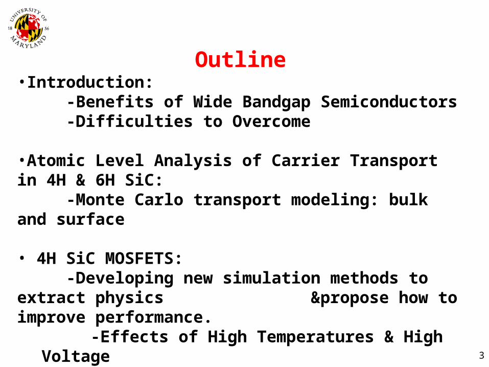
Outline•Introduction:
-Benefits of Wide Bandgap Semiconductors-Difficulties to Overcome
•Atomic Level Analysis of Carrier Transport in 4H & 6H SiC: -Monte Carlo transport modeling: bulk and surface
• 4H SiC MOSFETS: -Developing new simulation methods to extract physics
&propose how to improve performance.-Effects of High Temperatures & High Voltage
-4H MOSFET-Improved numerical attributes
4
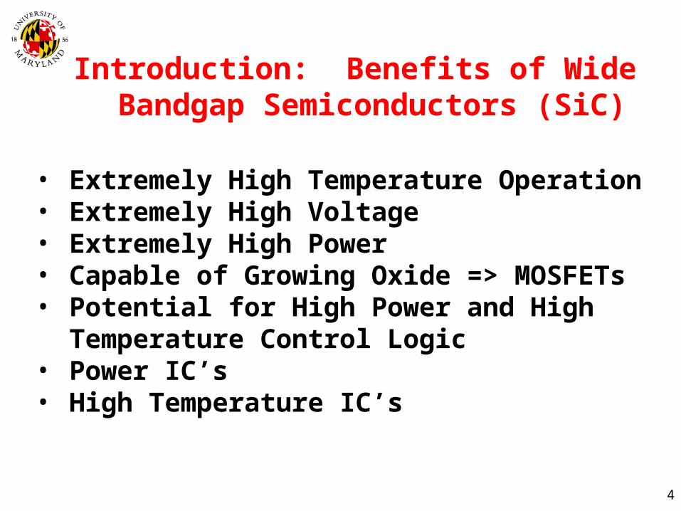
Introduction: Benefits of Wide Bandgap Semiconductors (SiC)
• Extremely High Temperature Operation• Extremely High Voltage• Extremely High Power• Capable of Growing Oxide => MOSFETs• Potential for High Power and High Temperature
Control Logic• Power IC’s• High Temperature IC’s
5
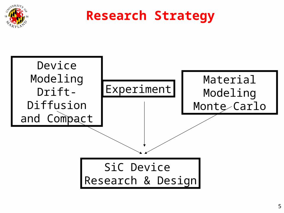
Research Strategy
Device ModelingDrift-Diffusion and Compact
Material ModelingMonte CarloExperiment
SiC Device Research & Design
6
Advanced Drift Diffusion Device Simulator
for 6H and 4H-SiC MOSFETs
7
Outline
Brief introduction to Silicon Carbide Mobility Modeling for 4H-SiC MOSFETs
Coulomb Scattering Mobility Model Simulations and Extracted Results Conclusion
8
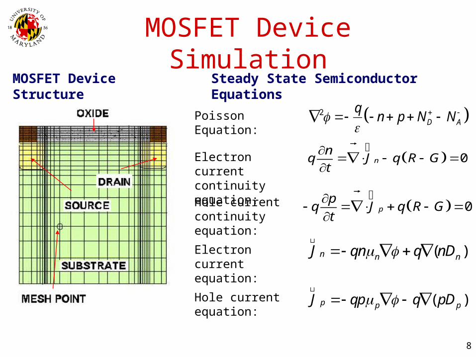
MOSFET Device Structure Steady State Semiconductor Equations
2D A
qn p N N
Poisson Equation:
0nn
q J q R Gt
��������������Electron current continuity equation:
0pp
q J q R Gt
��������������Hole current continuity equation:
( )n n nJ qn q nD ��������������
Electron current equation:
( )p p pJ qp q pD ��������������
Hole current equation:
MOSFET Device Simulation
9
Mobility Models
High Field Mobility:
Matthiessen's rule
CSRSPBLF 11111
LF = Low Field Mobility B = Bulk Mobility
SP = Surface Phonon Mobility
SR = Surface Roughness mobility
C = Coulomb Scattering Mobility
Low field mobility:
||1
LFHF
LF
sat
E
v
High field mobility:
Oxide
Bulk
Electron Flow
Electron Surface Phonon
Surface RoughnessTrap
Fixed Charge
10
Why a Coulomb Mobility Model?
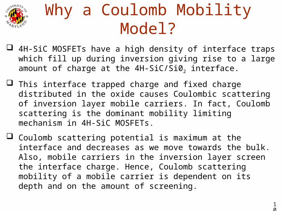
4H-SiC MOSFETs have a high density of interface traps which fill up during inversion giving rise to a large amount of charge at the 4H-SiC/Si02 interface.
This interface trapped charge and fixed charge distributed in the oxide causes Coulombic scattering of inversion layer mobile carriers. In fact, Coulomb scattering is the dominant mobility limiting mechanism in 4H-SiC MOSFETs.
Coulomb scattering potential is maximum at the interface and decreases as we move towards the bulk. Also, mobile carriers in the inversion layer screen the interface charge. Hence, Coulomb scattering mobility of a mobile carrier is dependent on its depth and on the amount of screening.
11
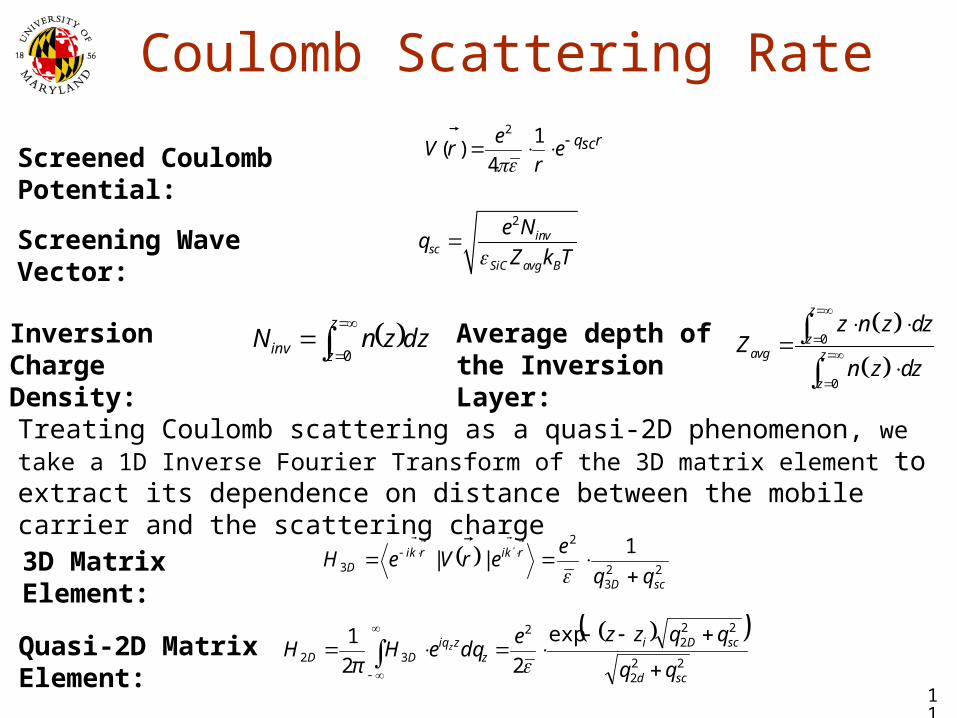
Coulomb Scattering Raterscqe
r
erV
1
4)(
2
Screened Coulomb Potential:
2inv
scSiC avg B
e Nq
Z k TScreening Wave Vector:
Quasi-2D Matrix Element:
22
3
2
3
1||
scD
rkirkiD
qq
eerVeH
22
2
222
2
32
exp
22
1
scd
scDiz
ziqDD
qq
qqzzedqeH
πH z
3D Matrix Element:
z
zinv dzznN0
0
0
z
zavg z
z
z n z dzZ
n z dz
Inversion Charge Density:
Average depth of the Inversion Layer:
Treating Coulomb scattering as a quasi-2D phenomenon, we take a 1D Inverse Fourier Transform of the 3D matrix element to extract its dependence on distance between the mobile carrier and the scattering charge
12
Coulomb Scattering Rate
2
0 0
0it f i
D if i i
N N zN z
N z z
Scattering Charge Distribution
Quasi-2D Scattering Rate: 22
0 0
11 cos
, 4D i
k ki k
N zk dk d
z z
For the results shown in this paper, we have assumed that the fixed oxide charge is located at the interface.
ElectronScattering Charge
z=zi=0
zS D
zi
Bulk
dzzqTkm
qTkm
qTzzF isc
eB
sceB
scei sin
82exp
sin8
1 ,,2
0
222
*
222
*
2
ei
eB
iD
eiC
TzzFTk
zNem
e
m
Tzz,,
16
1
,,
12
23**
iz eiCeC TzzTz ,,
1
,
1
Coulomb Scattering Mobility:
Total Coulomb Mobility at depth z:
13
Comments on the Coulomb Mobility Model
The model is easy to implement in a drift diffusion device simulator as it gives local mobility everywhere inside the device
Coulomb mobility is directly proportional to temperature and inversely proportional to the density of scattering charge
For a constant scattering charge density, Coulomb mobility will increase with gate voltage due to increased screening
Coulomb mobility increases rapidly with distance away from the interface
Effect of oxide charges distributed inside the oxide away from the interface is less on determining the scattering of inversion layer charges
14
4H-SiC MOSFET Simulationsand Extracted Results
15
Room Temperature ID-VGS
0 5 10 150
1
2
3
4
5
x 10-6
VGS
(Volts)
I D (
A)
Simulation
Experiment
VDS
=0.25V
T = 300oK
-5 0 5 10 1510
-9
10-8
10-7
10-6
10-5
VGS
(Volts)
I D (A
)Simulation
Experiment
VDS
=0.25V
T = 300oK
16
Interface Trap Density of States
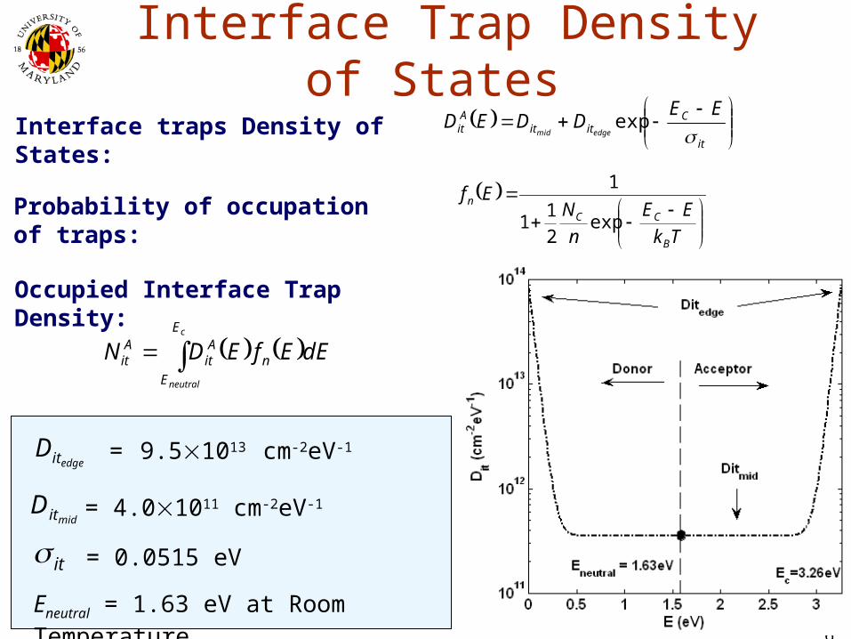
Interface traps Density of States:
Probability of occupation of traps:
Occupied Interface Trap Density:
it
Citit
Ait
EEDDED
edgemid exp
Tk
EE
n
NEf
B
CC
n
exp2
11
1
c
neutral
E
E
nA
itA
it dEEfEDN
edgeitD
miditD
it
= 9.51013 cm-2eV-1
= 4.01011 cm-2eV-1
= 0.0515 eV
Eneutral = 1.63 eV at Room Temperature
17
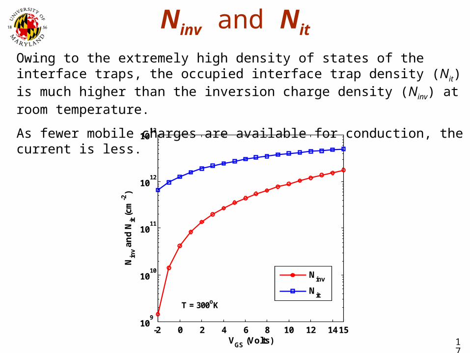
Ninv and Nit
-2 0 2 4 6 8 10 12 141510
9
1010
1011
1012
1013
VGS
(Volts)
Nin
v an
d N
it (
cm
-2)
Ninv
Nit
T = 300oK
Owing to the extremely high density of states of the interface traps, the occupied interface trap density (Nit) is much higher than the inversion charge density (Ninv) at room temperature.
As fewer mobile charges are available for conduction, the current is less.
18
Coulomb Scattering Mobility
0 2 4 6 8 10 1210
1
102
103
104
105
Depth (nm)
Co
ulo
mb
Mo
bili
ty (
cm
2/V
s)
VGS
= -2V
VGS
= 2VV
GS = 6V
VGS
= 10V
VGS
= 14V
T = 300oK
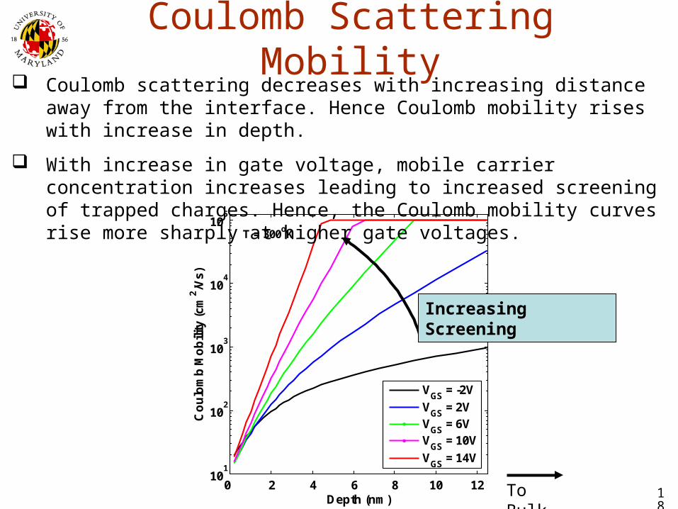
Coulomb scattering decreases with increasing distance away from the interface. Hence Coulomb mobility rises with increase in depth.
With increase in gate voltage, mobile carrier concentration increases leading to increased screening of trapped charges. Hence, the Coulomb mobility curves rise more sharply at higher gate voltages.
Increasing Screening
To Bulk
19
Total Low Field Mobility vs. Depth
0 2 4 6 8 10 120
50
100
150
200
250
300
350
Depth (nm)
To
tal L
ow
Fie
ld M
ob
ility
(c
m2/V
s)
VGS
= -2V
VGS
= 0V
VGS
= 2V
VGS
= 6V
VGS
= 8V
T = 300oK
The total mobility increases with depth inside the 4H-SiC MOSFET.
At the surface, the total low field mobility is approximately 25 cm2/Vs at room temperature.
To BulkSurface Mobility20 cm2/Vs - 30 cm2/Vs
20
Effect of Screening
0 2 4 6 8 10 1210
1
102
103
104
105
Depth (nm)
Mo
bili
ty (
cm2/V
s)
Cu
rren
t Den
sity
(A/c
m2)
SR
C
Total
Jn
VGS
= 12V
T = 300oK
0 2 4 6 8 10 1210
0
101
102
103
104
Depth (nm)
Mo
bili
ty (
cm2/V
s)
Cu
rren
t Den
sity
(A/c
m2)
SR
C
Total
Jn
VGS
= 2V
T = 300oK
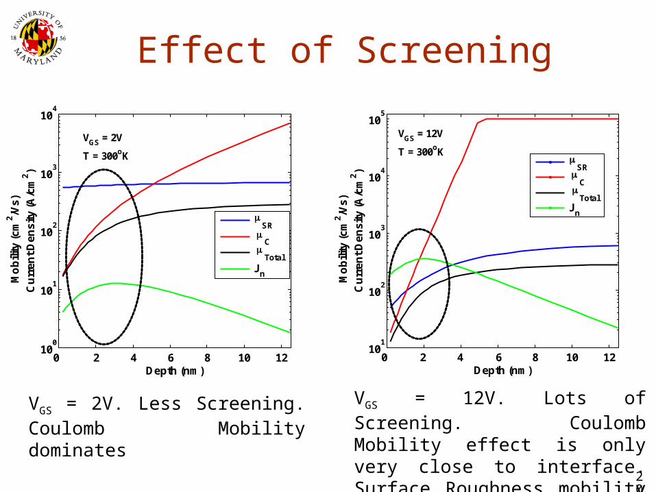
VGS = 2V. Less Screening. Coulomb Mobility dominates
VGS = 12V. Lots of Screening. Coulomb Mobility effect is only very close to interface. Surface Roughness mobility dominates
21
Current Density
0 2 4 6 8 10 120
50
100
150
200
250
300
350
400
450
Depth (nm)
Cu
rre
nt
De
ns
ity
(A
/cm
2)
VGS
= 0VV
GS = 2V
VGS
= 4VV
GS = 6V
VGS
= 8VV
GS = 10V
VGS
= 12VV
GS = 14V
T = 300oK
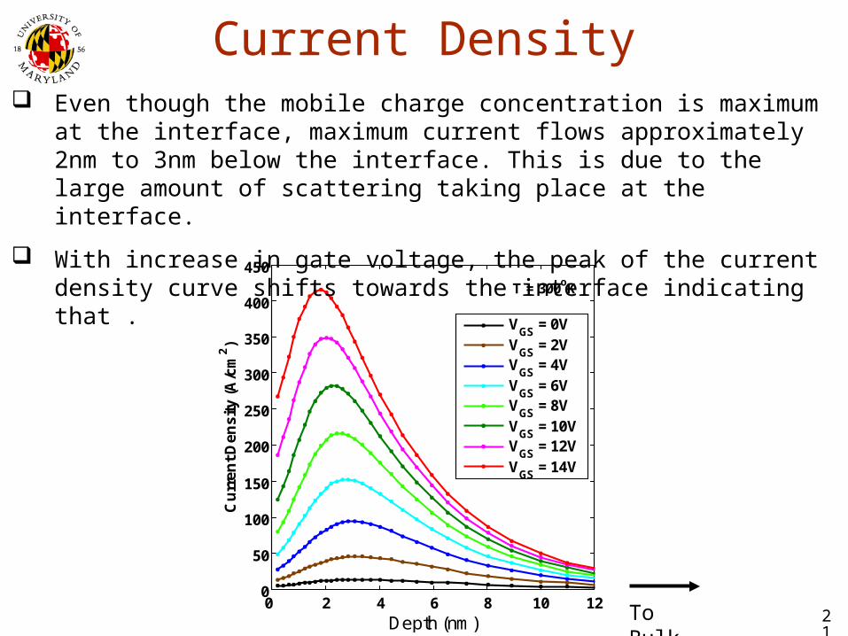
Even though the mobile charge concentration is maximum at the interface, maximum current flows approximately 2nm to 3nm below the interface. This is due to the large amount of scattering taking place at the interface.
With increase in gate voltage, the peak of the current density curve shifts towards the interface indicating that .
To Bulk
22
Improving the Interface
0 5 10 150
1
2
3
4
5
6
7
8x 10
-6
VGS
(Volts)
I D (
A)
Fit to ExperimentFactor of 10 ReductionFactor of 100 Reduction
VDS
=0.25V
T = 300oK
0 5 10 150
0.2
0.4
0.6
0.8
1
1.2
1.4x 10
-5
VGS
(Volts)
I D (
A)
Fit to ExperimentFactor of 10 ReductionFactor of 100 Reduction
VDS
=0.25V
T = 300oK
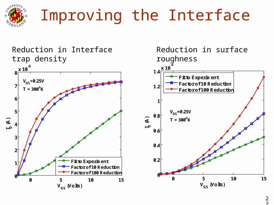
Reduction in Interface trap density Reduction in surface roughness
23
Coulomb Mobility: Key Findings & Remarks
Room temperature models for different types of mobilities have been devised and implemented for 4H-SiC MOSFETs, and good agreement between simulations and experiment has been achieved.
A first principles Coulomb Scattering mobility model has been developed specifically for 4H-SiC MOSFETs
Interface trap density of states for 4H-SiC MOSFETs has been estimated
Coulomb scattering due to interface trapped charge and surface roughness scattering are the two dominant mobility degradation mechanisms
Maximum current flows 2nm – 3nm away from the interface in 4H-SiC MOSFETs
Large improvement in current is predicted on reduction of interface trap densities in 4H-SiC MOSFETs
24
Roughness Mobility for a 4H-SiC Roughness Mobility for a 4H-SiC Stepped SurfaceStepped Surface
25
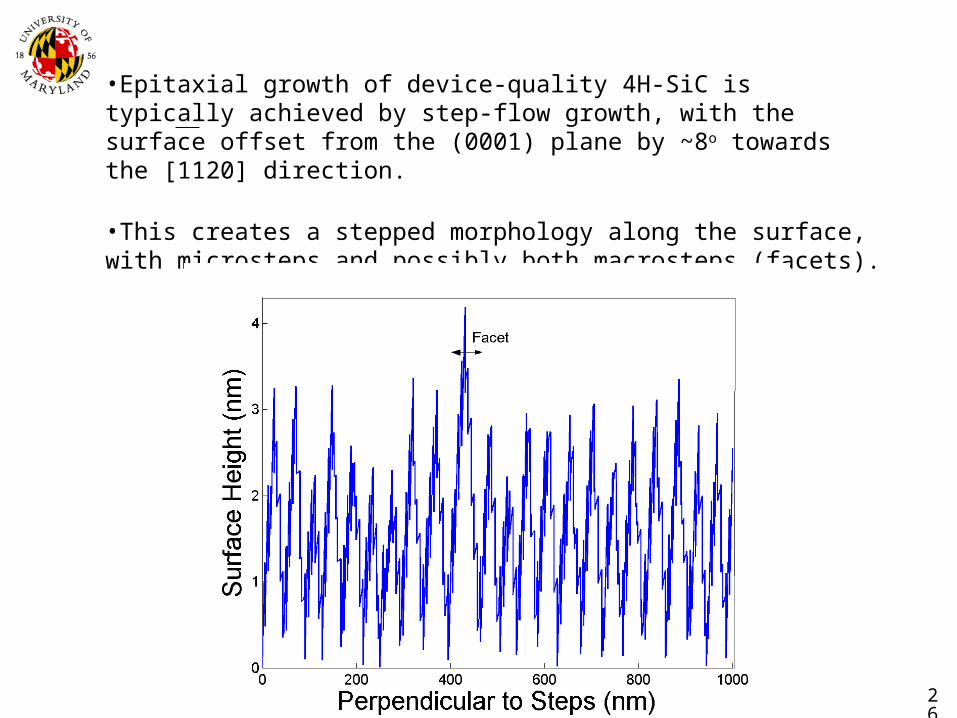
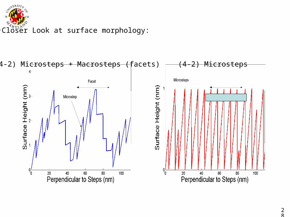
Surface MorphologySurface Morphology
26
•Epitaxial growth of device-quality 4H-SiC is typically achieved by step-flow growth, with the surface offset from the (0001) plane by ~8o towards the [1120] direction.
•This creates a stepped morphology along the surface, with microsteps and possibly both macrosteps (facets).
27
•Surface morphology is generated via Monte Carlo methods using experimental observations.•Step width distribution indicates meandering, but will use straight steps for now. •Random roughness parallel and perpendicular to steps (L, d)
00.10.20.30.40.50.60.7
1 2 3 4 5 6 7 8
Number of Bilayers at Microstep
Probability
Kimoto et al. J. Appl. Phys. V 81, p3494 (1997)Microsteps (4-2 bunching)
Syväjärvi et al. J. Crystal Growth. V 236, p297 (2002)Macrosteps
• Meandering of steps is not included at this point. This effect increases as the distribution of step widths increases. • Microsteps will meander if step bunching occurs. (increase in || roughness)
~40nm facet
~6nm micostep
Meandering of microsteps on a facet
30
Roughness Scattering at Roughness Scattering at 4H-SiC/oxide interface4H-SiC/oxide interface
31
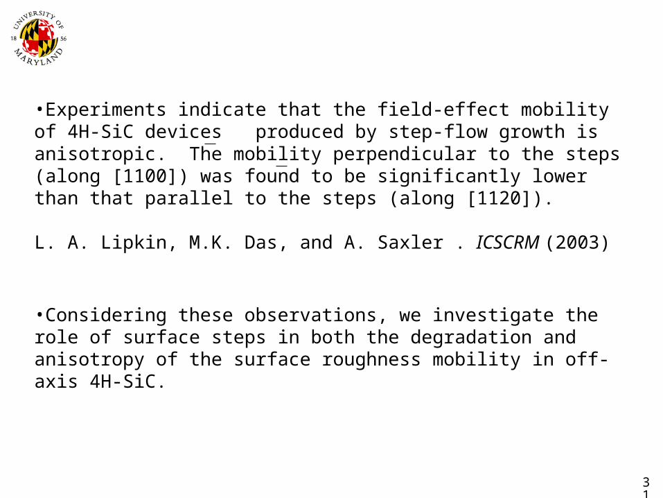
•Experiments indicate that the field-effect mobility of 4H-SiC devices produced by step-flow growth is anisotropic. The mobility perpendicular to the steps (along [1100]) was found to be significantly lower than that parallel to the steps (along [1120]).
L. A. Lipkin, M.K. Das, and A. Saxler . ICSCRM (2003)
•Considering these observations, we investigate the role of surface steps in both the degradation and anisotropy of the surface roughness mobility in off-axis 4H-SiC.
32
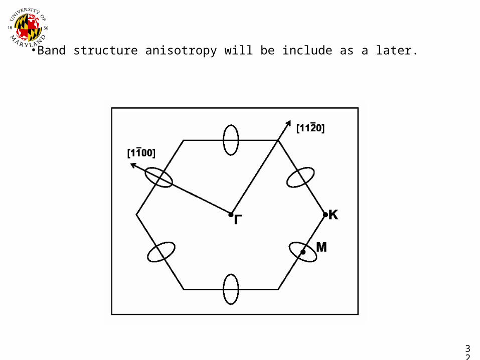
•Band structure anisotropy will be include as a later.
33
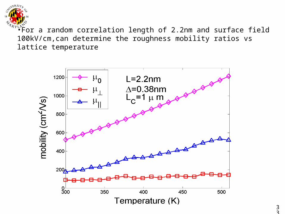
•For a random correlation length of 2.2nm and surface field 100kV/cm,can determine the roughness mobility ratios vs lattice temperature
34
Carrier relaxation rate due to surface roughness
Momentum relaxation rate for carrier with (kx,ky):
• Γ=image potential correction, set =1 • θ = (kxqx + kyqy) |(kxqx + kyqy)| • F=surface field (1X10⁵ V/cm used here)
• ε=ε(F), screening dielectric function
35
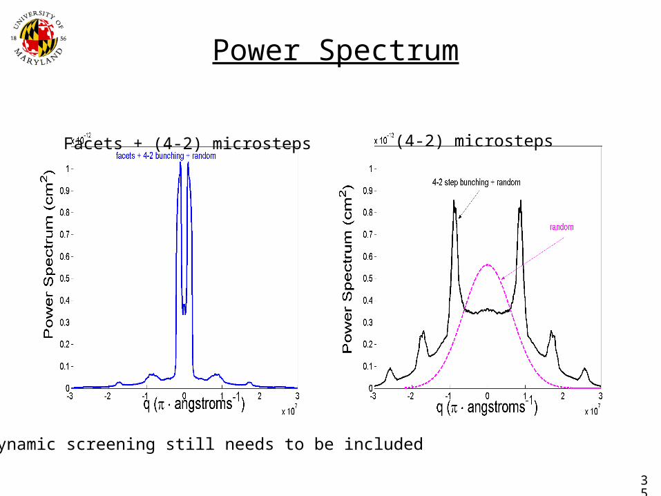
Facets + (4-2) microsteps (4-2) microsteps
Power Spectrum
•Dynamic screening still needs to be included
36
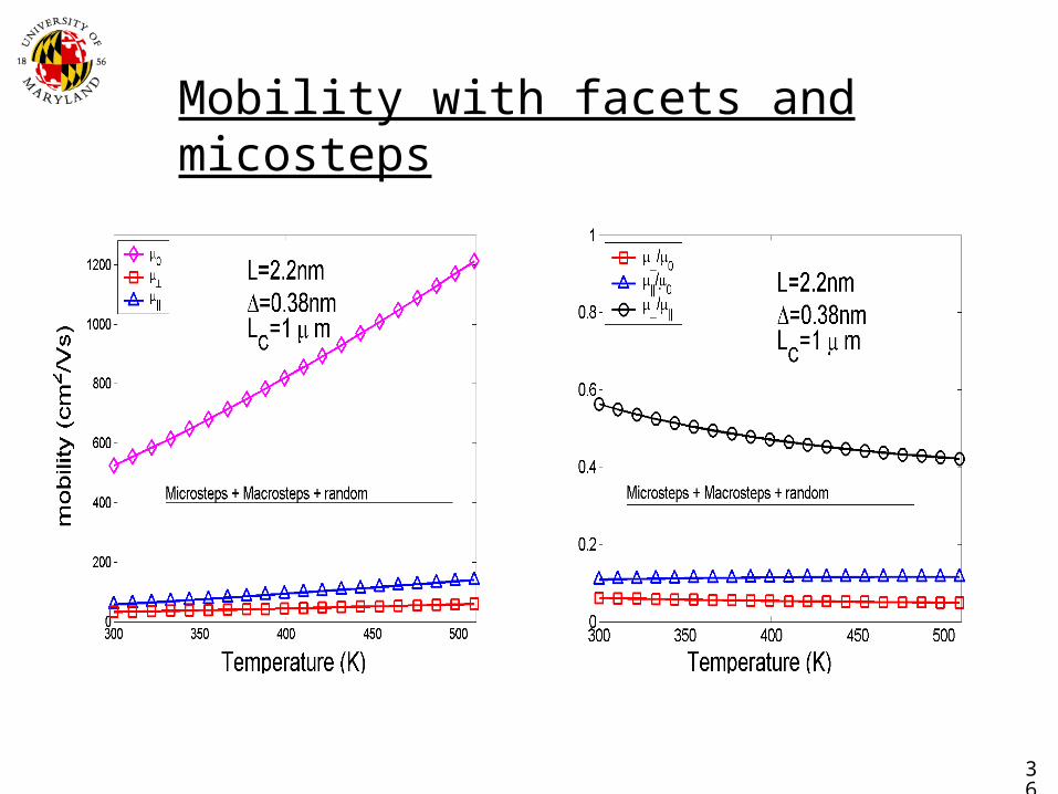
Mobility with facets and micosteps
37
Mobility without facets
38
00.10.20.30.40.50.60.7
1 2 3 4 5 6 7 8
Number of Bilayers at Microstep
Probability
0
0.05
0.1
0.15
0.2
0.25
0.3
1 2 3 4 5 6 7 8
Number of Bilayers at Microstep
Probability
0
0.2
0.4
0.6
0.8
1
1 2 3 4 5 6 7 8
Number of Bilayers at Microstep
Probability
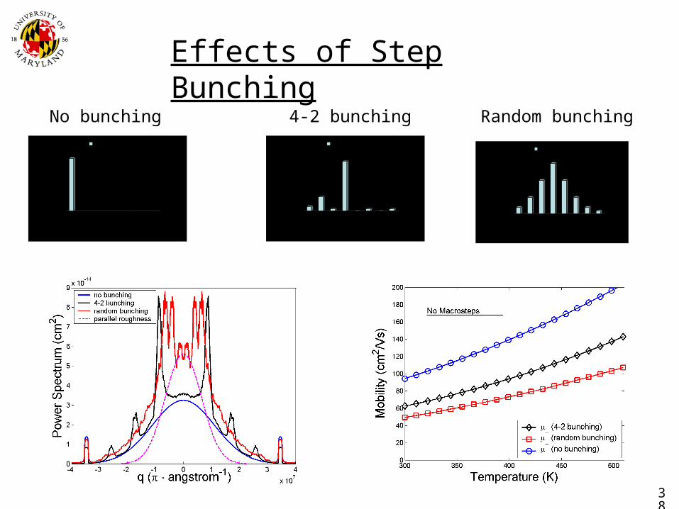
No bunching 4-2 bunching Random bunching
Effects of Step Bunching
39
Conclusions
•The presence of the surface steps reduces the mobility of 4H-SiC by a factor of 5-10.
•With L=2.2nm, mobilities increase approximately linearly with T.
•4H-SiC devices operating at high temperatures should have an enhancement of the surface roughness mobility when compared to room temperature operation. Microsteps appear to reduce the anisotropy with increasing temperature whereas faceting appears to have the opposite effect.
Step bunching significantly degrades the roughness mobility.
40
Key Results for Recent 4H SiC Technology
• Significant improvement in numerical attributes of simulator:– Allows for much higher resolution mesh
• Improved physical model for interface state mobility – Depends on 2D coulomb scattering
• Developing new model for device instability– Use gate current injected from channel– Related to oxide charging and interface trap generation
• New Monte Carlo simulations show energy of carriers in channel– Needed for interface trap generation – Needed for oxide state occupation
41
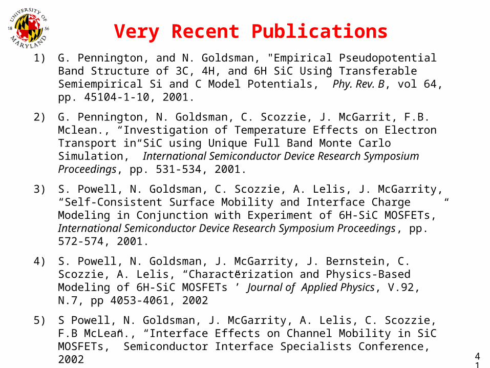
1) G. Pennington, and N. Goldsman, "Empirical Pseudopotential Band Structure of 3C, 4H, and 6H SiC Using Transferable Semiempirical Si and C Model Potentials,” Phy. Rev. B, vol 64, pp. 45104-1-10, 2001.
2) G. Pennington, N. Goldsman, C. Scozzie, J. McGarrit, F.B. Mclean., “Investigation of Temperature Effects on Electron Transport in SiC using Unique Full Band Monte Carlo Simulation,” International Semiconductor Device Research Symposium Proceedings, pp. 531-534, 2001.
3) S. Powell, N. Goldsman, C. Scozzie, A. Lelis, J. McGarrity, “Self-Consistent Surface Mobility and Interface Charge Modeling in Conjunction with Experiment of 6H-SiC MOSFETs,” International Semiconductor Device Research Symposium Proceedings, pp. 572-574, 2001.
4) S. Powell, N. Goldsman, J. McGarrity, J. Bernstein, C. Scozzie, A. Lelis, “Characterization and Physics-Based Modeling of 6H-SiC MOSFETs”’ Journal of Applied Physics, V.92, N.7, pp 4053-4061, 2002
5) S Powell, N. Goldsman, J. McGarrity, A. Lelis, C. Scozzie, F.B McLean., “Interface Effects on Channel Mobility in SiC MOSFETs,” Semiconductor Interface Specialists Conference, 2002
6) G. Pennington, S. Powell, N. Goldsman, J.McGarrity, A. Lelis, C.Scozzie., “Degradation of Inversion Layer Mobility in 6H-SiC by Interface Charge,” Semiconductor Interface Specialists Conference, 2002.
Very Recent Publications
42
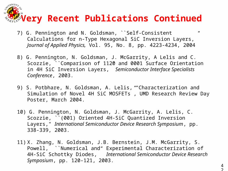
7) G. Pennington and N. Goldsman, ``Self-Consistent Calculations for n-Type Hexagonal SiC Inversion Layers,” Journal of Applied Physics, Vol. 95, No. 8, pp. 4223-4234, 2004
8) G. Pennington, N. Goldsman, J. McGarrity, A Lelis and C. Scozzie, ``Comparison of 1120 and 0001 Surface Orientation in 4H SiC Inversion Layers,” Semiconductor Interface Specialists Conference, 2003.
9) S. Potbhare, N. Goldsman, A. Lelis, “Characterization and Simulation of Novel 4H SiC MOSFETs”, UMD Research Review Day Poster, March 2004.
10) G. Pennington, N. Goldsman, J. McGarrity, A. Lelis, C. Scozzie, ``(001) Oriented 4H-SiC Quantized Inversion Layers," International Semiconductor Device Research Symposium, pp. 338-339, 2003.
11) X. Zhang, N. Goldsman, J.B. Bernstein, J.M. McGarrity, S. Powell, ``Numerical and Experimental Characterization of 4H-SiC Schottky Diodes,” International Semiconductor Device Research Symposium, pp. 120-121, 2003.
12) S. K. Powell, N. Goldsman, A. Lelis, J. M. McGarrity and F.B. McLean, High Temperature Modeling and Characterization of 6H SiC MOSFETs, Journal of Applied Physics, 2005.
Very Recent Publications Continued
43
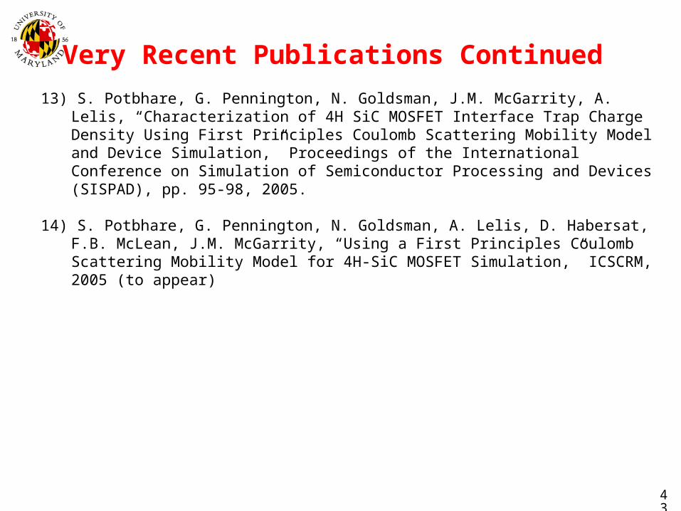
13) S. Potbhare, G. Pennington, N. Goldsman, J.M. McGarrity, A. Lelis, “Characterization of 4H SiC MOSFET Interface Trap Charge Density Using First Principles Coulomb Scattering Mobility Model and Device Simulation,” Proceedings of the International Conference on Simulation of Semiconductor Processing and Devices (SISPAD), pp. 95-98, 2005.
14) S. Potbhare, G. Pennington, N. Goldsman, A. Lelis, D. Habersat, F.B. McLean, J.M. McGarrity, “Using a First Principles Coulomb Scattering Mobility Model for 4H-SiC MOSFET Simulation,” ICSCRM, 2005 (to appear)