23
1 Recap: Memory Hierarchy
| Date post: | 16-Dec-2015 |
| Category: |
Documents |
| Upload: | nora-morris |
| View: | 228 times |
| Download: | 0 times |

1
Recap: Memory Hierarchy
2
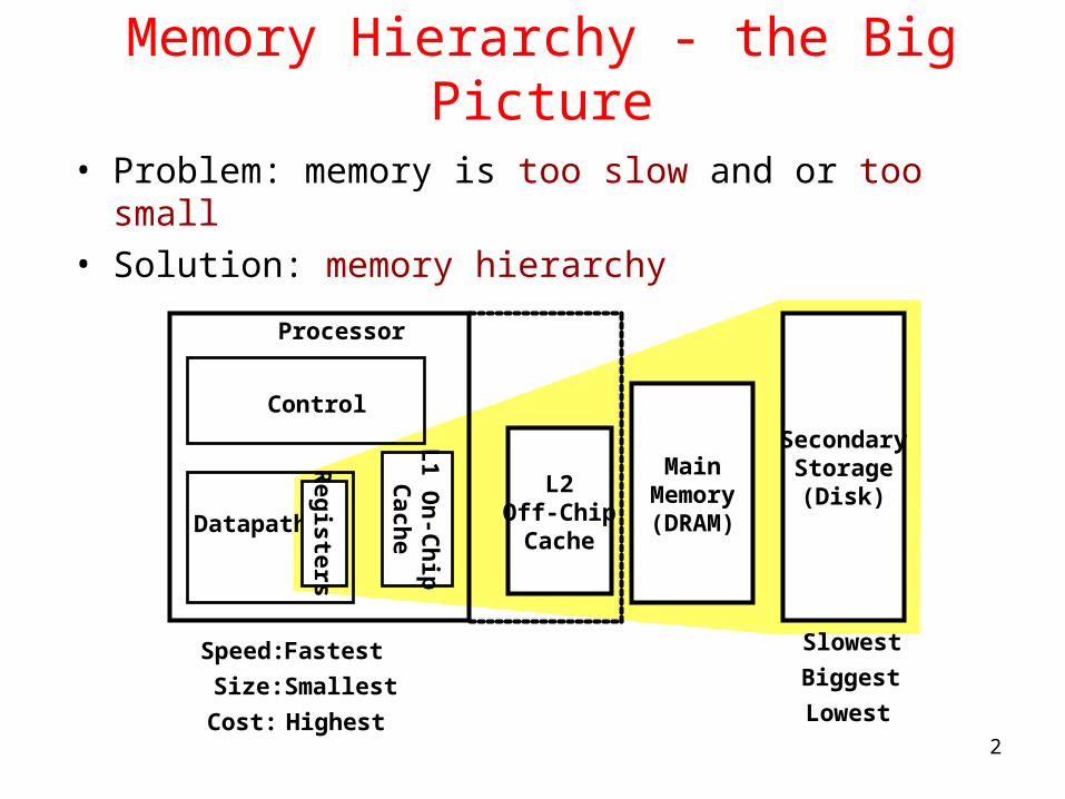
Memory Hierarchy - the Big Picture
• Problem: memory is too slow and or too small• Solution: memory hierarchy
Fastest Slowest
Smallest Biggest
Highest Lowest
Speed:
Size:
Cost:
Control
Datapath
SecondaryStorage(Disk)
Processor
Registers
L2Off-Chip
Cache
MainMemory(DRAM)
L1 O
n-C
hip
Cach
e

3
Why Hierarchy Works• The principle of locality
– Programs access a relatively small portion of the address space at any instant of time.
– Temporal locality: recently accessed instruction/data is likely to be used again– Spatial locality: instruction/data near recently accessed /instruction data is likely to be used soon
• Result: the illusion of large, fast memory
Address Space0 2n - 1
Probabilityof reference
4
Example of Locality
int A[100], B[100], C[100], D; for (i=0; i<100; i++) {
C[i] = A[i] * B[i] + D;}
A[0]A[1]A[2]A[3]A[5]A[6]A[7] A[4]
A[96]A[97]A[98]A[99]B[1]B[2]B[3] B[0]
. . . . . . . . . . . . . .
B[5]B[6]B[7] B[4]B[9]B[10]B[11] B[8]
C[0]C[1]C[2]C[3]C[5]C[6]C[7] C[4]
. . . . . . . . . . . . . .
. . . . . . . . . . . . . .
C[96]C[97]C[98]C[99]D

5
Four Key Cache Questions:
1.Where can block be placed in cache? (block placement)
2.How can block be found in cache? …using a tag(block identification)
3.Which block should be replaced on a miss? (block replacement)
4.What happens on a write? (write strategy)

6
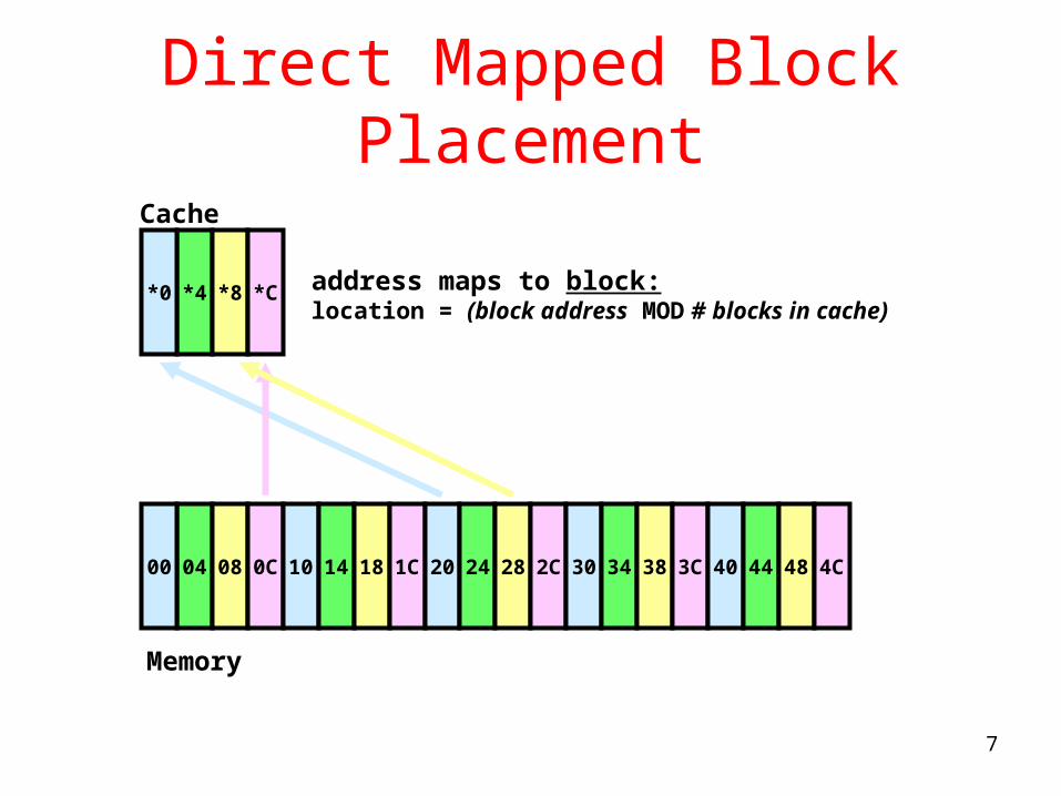
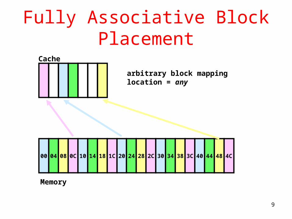
Q1: Block Placement
• Where can block be placed in cache?– In one predetermined place - direct-mapped
• Use fragment of address to calculate block location in cache• Compare cache block with tag to test if block present
– Anywhere in cache - fully associative• Compare tag to every block in cache
– In a limited set of places - set-associative• Use address fragment to calculate set• Place in any block in the set• Compare tag to every block in set• Hybrid of direct mapped and fully associative
7
Direct Mapped Block Placement
*4*0 *8 *C
Cache
0400 08 0C 10 14 18 1C 20 24 28 2C 30 34 38 3C 40 44 48 4C
Memory
address maps to block:location = (block address MOD # blocks in cache)

8
0xF011111
11111 0xAA
0x0F00000
00000 0x55
Direct Mapping
0
1
000001
0
1
0
10x0F00000
00000 0x55
11111 0xAA
0xF011111
Tag Index Data
Direct mapping:A memory value can only be placed at a single corresponding location in the cache
9
Fully Associative Block Placement
0400 08 0C 10 14 18 1C 20 24 28 2C 30 34 38 3C 40 44 48 4C
Cache
Memory
arbitrary block mappinglocation = any
10
0xF01111
1111 0xAA
0x0F0000
0000 0x55
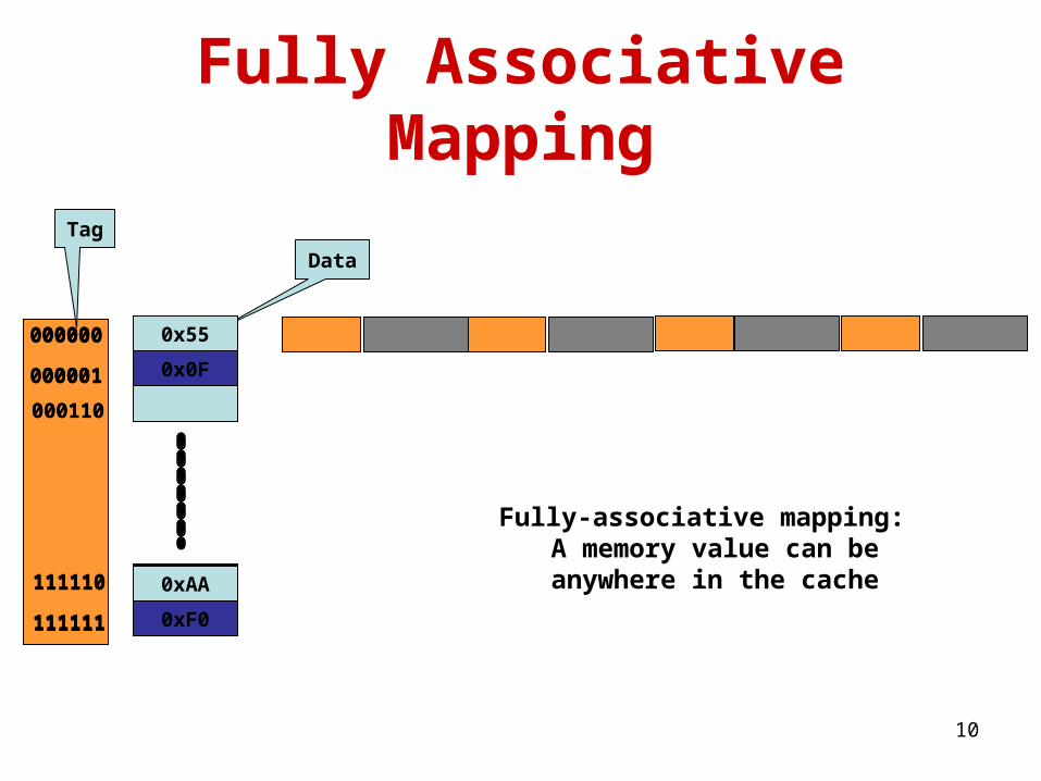
Fully Associative Mapping
0x0F
0x55
0xAA
0xF0
Tag
Data
000110
000001
000000
111110
111111 0xF01111
1111 0xAA
0x0F0000
0000 0x55
0x0F
0x55
0xAA
0xF0
000110
000001
000000
111110
111111
Fully-associative mapping:A memory value can be anywhere in the cache

11
Set-Associative Block Placement
0400 08 0C 10 14 18 1C 20 24 28 2C 30 34 38 3C
*4*0 *8 *C
40 44 48 4C
Cache
Memory
*0 *4 *8 *C
Set 0 Set 1 Set 2 Set 3
address maps to set:location = (block address MOD # sets in cache)(arbitrary location in set)
12
0xF01111
1111 0xAA
0x0F0000
0000 0x55
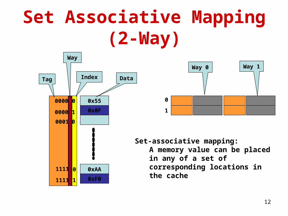
Set Associative Mapping (2-Way)
0
10x0F
0x55
0xAA
0xF0
Tag Index Data
00
01
100001
10
11
0000
0000
1111
1111
Way
Way 1Way 0
Set-associative mapping:A memory value can be placed in any of a set of corresponding locations in the cache
13
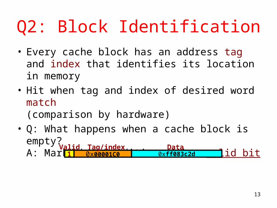
Q2: Block Identification• Every cache block has an address tag and index
that identifies its location in memory• Hit when tag and index of desired word match
(comparison by hardware)• Q: What happens when a cache block is empty?
A: Mark this condition with a valid bit
0x00001C0 0xff083c2d1Tag/indexValid Data

14
Direct-Mapped Cache Design
CACHE SRAM
ADDR
DATA[31:0]
0x00001C0 0xff083c2d01 0x0000000 0x000000211 0x0000000 0x000001030010 0x23F0210 0x00000009
1TagV Data
=
030x0000000
DATA[58:32]DATA[59]
DATA HITADDRESS =1TagCacheIndex
Byte Offset

15
Set Associative Cache Design• Key idea:
– Divide cache into sets– Allow block anywhere in a set
• Advantages:– Better hit rate
• Disadvantage:– More tag bits– More hardware– Higher access time
Address
22 8
V TagIndex
0
1
2
253
254255
Data V Tag Data V Tag Data V Tag Data
3222
4-to-1 multiplexor
Hit Data
123891011123031 0
A Four-Way Set-Associative Cache (Fig. 7.17)

16
tag 11110111 data 1111000011110000101011=
Fully Associative Cache Design• Key idea: set size of one block
– 1 comparator required for each block– No address decoding– Practical only for small caches due to hardware
demands
tag 00011100 data 0000111100001111111101=
=
=
=
=
tag 11111110
tag 00000011
tag 11100110
tag 11110111 data 1111000011110000101011
data 0000000000001111111100
data 1110111100001110000001
data 1111111111111111111111
tag in 11110111 data out 1111000011110000101011

17
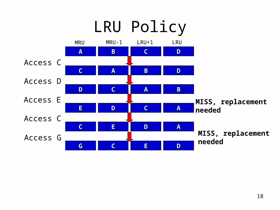
Cache Replacement Policy
• Random – Replace a randomly chosen line
• LRU (Least Recently Used)– Replace the least recently used line
18
LRU Policy
AA BB CC DD
MRU LRULRU+1MRU-1
Access CCC AA BB DD
Access DDD CC AA BB
Access EEE DD CC AA
Access CCC EE DD AA
Access GGG CC EE DD
MISS, replacement needed
MISS, replacement needed
19
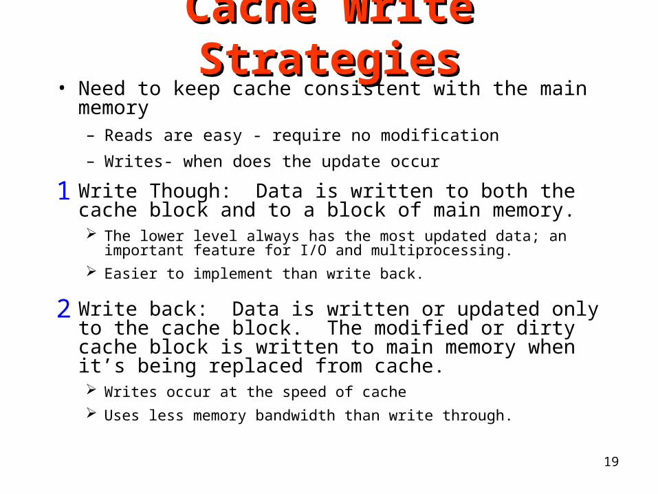
Cache Write Cache Write StrategiesStrategies
• Need to keep cache consistent with the main memory– Reads are easy - require no modification
– Writes- when does the update occur
1 Write Though: Data is written to both the cache block and to a block of main memory. The lower level always has the most updated data; an important feature
for I/O and multiprocessing.
Easier to implement than write back.
2 Write back: Data is written or updated only to the cache block. The modified or dirty cache block is written to main memory when it’s being replaced from cache. Writes occur at the speed of cache
Uses less memory bandwidth than write through.
20
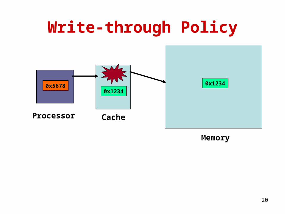
0x12340x1234
Write-through Policy
0x1234
Processor Cache
Memory
0x12340x56780x5678
21
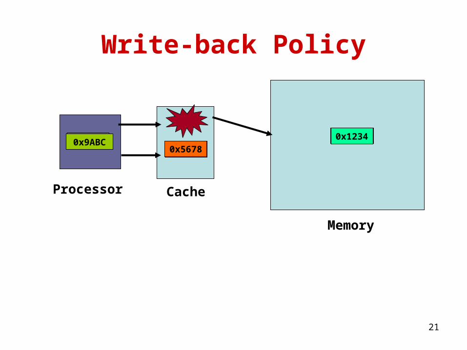
0x12340x1234
Write-back Policy
0x1234
Processor Cache
Memory
0x12340x5678
0x56780x56780x9ABC

22
Write Buffer for Write Write Buffer for Write ThroughThrough
• A Write Buffer is needed between the Cache and Memory
– Processor: writes data into the cache and the write buffer– Memory controller: write contents of the buffer to memory
• Write buffer is just a FIFO:– Typical number of entries: 4– Works fine if: Store frequency (w.r.t. time) << 1 / DRAM
write cycle
ProcessorCache
Write Buffer
DRAM
23
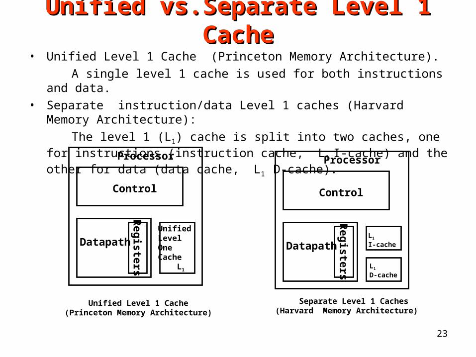
Unified vs.Separate Level 1 Unified vs.Separate Level 1 CacheCache
• Unified Level 1 Cache (Princeton Memory Architecture).
A single level 1 cache is used for both instructions and data.
• Separate instruction/data Level 1 caches (Harvard Memory Architecture):
The level 1 (L1) cache is split into two caches, one for instructions (instruction cache, L1 I-cache) and the other for data (data cache, L1 D-cache).
Control
Datapath
Processor
Registers
UnifiedLevel OneCache L1
Control
Datapath
Processor
Registers
L1
I-cache
L1
D-cache
Unified Level 1 Cache (Princeton Memory Architecture)
Separate Level 1 Caches (Harvard Memory Architecture)


