Page 1
7/28/2019 1-s2.0-S0040609005024570-main
http://slidepdf.com/reader/full/1-s20-s0040609005024570-main 1/7
Electrical characterization of novel Si solar cells
O. Tuzun a,*, S. Oktik a , S. Altindal b, T.S. Mammadov c
a Physics Department, Mugla University, 48000 Mugla, Turkey b Physics Department, Gazi University, 06500 Ankara, Turkey
c Institute of Physics, Baku, AZ 1143, Azerb aijan
Available online 25 January 2006
Abstract
A new approach for hybrid metal-insulator-semiconductor Si solar cells is adopted by the Institute of Fundamental Problems for High
Technology, Ukrainian Academy of Sciences. In this technique, the porous silicon layers are created on both sides of single crystal wafers by
chemical etching before an improved MIS cell preparation process. Using this technique, the solar cells with efficiencies above 15% have been
obtained under AM1.5 condition (under 100 mW/cm2 illumination at 25 -C). In this work the dark current–voltage–temperature ( I – V – T )
characteristics of these cells are studied over a temperature range between 79 and 400 K. The dark capacitance–voltage ( C – V ) and conductance –
voltage ( G – V ) behaviours of these cells at 100 kHz are analysed for the same temperature range. At room temperature C – V and G – V
measurements are also made under illumination levels changing five folds. The diode ideality factors calculated from the dark I – V characteristics
are significantly larger than unity and exhibit strong temperature dependence. The analysis of the temperature tendencies of diode ideality factor in
these cells indicated that the current transport mechanism consists of both the trap-assisted tunnelling and the thermionic emission. While the
temperature decreases, the barrier height calculations from I – V – T and C – V – T measurements showed that /B( I ÀV ) decreases whereas
/B(C ÀV ) increases. The difference in /B( I ÀV ) and /B(C ÀV ) values and in their temperature dependence are explained by a model assuming
Gaussian distribution of barrier heights. All the results are analysed after series resistance corrections.
D 2005 Elsevier B.V. All rights reserved.
Keywords: Porous silicon; Solar cells; Series resistance; Current transport mechanisms
1. Introduction
Novel photovoltaic (PV) cells are fabricated by creation of
porous silicon layers on p-type monocrystalline Si wafers using
an electro-chemical etching before an improved MIS cell
preparation process. This novel fabrication process gives rise to
a formation of diffused and field-induced surface inversion
layers, a generation of metal-insulator-semiconductor junction.
In this approach, due to high quality starting materials andrapid low-temperature (<800 -C) processing a high minority
carrier life time is attainable; this, in turn, gives rise to a high
photogenerated current collection. The porous Si exhibits
unique properties. It works like a sunlight concentrator, light
scattering diffuser and re-emitter of sunlight as well as an
electrical isolator in the multilayer Si structure. Employing a
specific surface modification, porous Si improves the PV
efficiency in UV and NIR regions of solar spectra [1].
Today the main scientific and technical problems of PV solar
cells are relevant to the increase in the efficiency of solar cells
and to reduce in the energy losses within the integrated PV
modules. The efficiency of solar cell depends on various factors
such as interface preparation process, metal to semiconductor
barrier height, device temperature, insulator layer formation and
series resistance. The most important advantage of using porous
Si in solar cells is its band gap which behaves as a direct band
gap semiconductor with large quantum efficiency and may beadjusted for optimum sunlight absorption. This device is
interesting because of the possibility for developing a low-cost
low-temperature fabrication process for terrestrial solar cells
having efficiencies of !17%. Therefore, in some recent works,
PV properties of highly efficient porous Si type and metal-
insulator-semiconductor (MIS) type solar cell structures have
been extensively studied and reported in the literature for more
than three decades [1 – 17]. However, very little attention has
been paid to the temperature, external illumination level and
voltage dependence of solar cells in the literature [9], especially
at low temperature.
0040-6090/$ - see front matter D
2005 Elsevier B.V. All rights reserved.doi:10.1016/j.tsf.2005.12.104
* Corresponding author. Tel.: +90 252 211 16 06; fax: +90 252 223 92 74.
E-mail address: [email protected] (O. Tuzun).
Thin Solid Films 511 –512 (2006) 258 – 264
www.elsevier.com/locate/tsf
Page 2
7/28/2019 1-s2.0-S0040609005024570-main
http://slidepdf.com/reader/full/1-s20-s0040609005024570-main 2/7
The characterization of interface states and series resistance
in solar cells and Schottky diodes have become the subject of
very intensive researches and have been repor ted in the
literature for more than four decades [11,18–22]. When the
solar cell has a series resistance Rs,, the voltage drop across the
junction is less than the applied voltage between the terminals
of solar cells. There are several experimental methods for calculating Rs from dark and illumination I – V measurements
at a series of different light intensities, but it can also be
deduced from admittance measurements (C – V and G – V ) as a
function of both temperature and external illumination intensity
level. Because of that, this method is suitable and reliable for
metal-insulator-semiconductor (MIS) or hybrid MIS type solar
cells and MIS diode. Due to the effect of parameters such as Rs
and interface states, characteristics of forward bias current–
voltage ( I – V ) and admittance (C – V and G – V ) at high voltages
deviate considerably from ideal behaviour [11,21,23,26–30].
Using this novel approach, the solar cells with efficiencies
above 15% under AM1.5 condition have been obtained. Thedark current– voltage– temperature ( I – V – T ) characteristics
of these cells are studied over a temperature range between
79 and 400 K. The dark capacitance –voltage (C ÀV ) and
conductance–voltage (G ÀV ) behaviours of these cells at 100
kHz are analysed for the same temperature range. At room
temperature, C – V and G – V measurements are also made under
illumination levels changing five folds. The ideality factors
calculated from the dark I – V characteristics are found to be
significantly larger than unity and exhibit strong temperature
dependency. The analysis of the temperature tendencies of diode
ideality factor in these cells indicated that the current transport
mechanism consists of both the trap-assisted tunnelling and the
thermionic emission. The barrier height calculations from I – V – T and C – V – T measurements showed that /B( I ÀV ) decreases
whereas /B(C ÀV ) increases with decreasing temperature. The
difference in /B( I ÀV ) and /B(C ÀV ) values and in their
temperature dependence are explained by a model assuming
Gaussian distribution of barrier heights. All the results were
analysed after series resistance corrections.
2. Experimental procedures
The PV solar cells were fabricated on boron doped p-type,
<100> single crystalline Si wafers (10.2 Â10.2 cm2 and 300 Am
thick). The doping level of wafers was about 2.77 Â1016
cmÀ3
showing with the resistivity of about 0.5 V cm. The structure of
this highly efficient novel porous silicon cell is given in Fig. 1.
The top and bottom sides of the base crystalline Si are modified
by etching processes and consist of layers and zones of porous Si
which looks like a sponge material with Si columns and pores
interconnected by hydrogen bonds. The top layer of porous Si is
thin enough (depth¨5 Am) to attain high anti-reflectivity and to
eliminate effect of high resistivity (105 –106V). To enhance the
profile distribution of potential barriers and p –n junction, it
includes arrays of porous Si pipes of special geometry. On the
face of the Si substrate there is a 10 nm thin layer of SiO2,
generated naturally in a chemical oxidation. At the top layer,
there is a 50 nm Ce2O3 layer on the SiO2. That dielectric layer
also executes three functions simultaneously: 1) anti-reflection
coating, 2) protection from radiation, and 3) induction of
inversion layer (depth of deposition ¨150 nm) with a
conductivity of n-type (Ce2O3 has a built-in positive charge
¨1012 cmÀ2). As a result, in the boundary between the layers of
p-type (base) and n-type (induced), the p –n junction arises. This
allows effective transformation of UV part of sunlight (0.25– 0.38 Am) since the depth of penetration of UV photons into the
material is within the range of 150 nm. Accordingly, the visible
and NIR sunlight (0.4– 0.9 Am) is absorbed in the large base area
of the cell surface. Absorbed photons form the charge carriers
(electron-hole pairs) which are separated at the p– n junction and
may diffuse through the semiconductor. While doing that, they
generate voltage and current (external circuit) drawn at metallic
contacts on the p and n surfaces of the cell. In order to more
effectively collect the carriers in the cell, the areas of p+-type (in
the base of the back contacts) and n+-type (under the front
contacts) are created by simultaneous diffusion of phosphorus
(towards the front side) and aluminium (towards the back side)
through the top and bottom layers of porous Si. These high-doping areas (doping levels N A= 5 Â1018 cmÀ3 and
N D= 1019 cmÀ3) form the driving electric fields, which
increase the mobility of carriers as well as collection factor
due to effect of diffusion and drift streams coupling. Metal/
porous-Si and porous-Si/crystalline-Si contacts are favourable
too. Besides, the profile of n+-type area with depth of ¨6
Am enlarges the area of p–n junction that in turn, enlarges a
number of carriers (electrons), which are potentially capable
(at a diffusion length ¨100 Am) to reach the p–n junction.
Depending on the reduction of surface reflectivity from 0.3
(polished Si) to 0.01–0.02 (porous Si), it has the best
characteristics among single layer AR coatings. It causes a25–40% increase in the short-circuit current of the PV cell. As
for metallic contacts, there are two variants. In the first one
(welding), there is Al grid on the back side and Al crested
collectors on the face side (spacing 2.5 mm, contact bandwidth
0.25 mm, width of collectors 2 mm). In the second one
(soldering), there are multilayer contacts: Mo–Cu–Ni on the
front side (n+-Si) and Al–Ti–Ni on the back side (p+-Si). The
last variant provides more effective contacts and reduces the
series resistance of interconnections in the cell.
The current– voltage ( I – V ), capacitance– voltage (C – V )
and conductance– voltage ( G – V ) characteristics of porous p-Si
solar cells at various temperatures are measured in the
temperature range of 79–400 K using temperature controlled
Fig. 1. Schematic diagram of a novel Si PV cell with porous silicon: 1, 4—top
and bottom contacts Al (Mo–Cu–Ni, Al–Ti–Ni); 2—crystalline Si of p-type;
3—porous Si of p+-type; 5—porous Si of n+-type + n-inversion layer; 6—AR
layer (porous Si+SiO2 – Ce2O3 TiO2).
O. Tuzun et al. / Thin Solid Films 511–512 (2006) 258–264 259
Page 3
7/28/2019 1-s2.0-S0040609005024570-main
http://slidepdf.com/reader/full/1-s20-s0040609005024570-main 3/7
Janes 475 cryostat. The I – V characteristics of the solar cells
are performed using a Keithley 220 programmable constant
current source and a Keithley 614 electrometer. The C – V and
G – V characteristics are performed at 100 kHz by using HP
4192A LF impedance analyzer (5 Hz–13 MHz).
3. Result and discussion
3.1. Efficiency measurements
The current–voltage ( I – V ) characteristics of porous silicon
solar cells obtained from both in dark and under illuminated
AM1.5 (100 mW/cm2) condition at room temperature are
shown in Fig. 2. The series resistance Rs is calculated from the
admittance measured in the strong accumulation according to
Nicollian [28]. We observed that from the admittance
measurements (C – V and G – V ), the increase of capacitance
C and conductance G under illumination are due to the
formation of an inversion layer at semiconductor –insulator interface as well as to interface states response.
The samples cut from high efficiency wafers (g >15%) are
tested under AM1.5 conditions (under 100 mW/cm2 illumina-
tion at 25 -C) [1]. As a typical example Fig. 2 shows the results
of a cell, with 2.76 cm2 area which exhibits a power conversion
efficiency of 15.3% with the open-circuit voltage (V oc), short-
circuit current density ( J sc) and the fill factor (FF) values of
605.7 mV, 32.66 mA/cm2 and 77.3%, respectively. The
efficiency values reported in this paper are for the active area
of the solar cells.
3.2. Dark current–voltage characteristics
A typical dark forward and reverse bias characteristic for the
novel Si solar cells in the temperature range from 79 to 400 K
are plotted as I – V graph shown in Fig. 3. Each plot consists of
a linear range with different slopes in intermediate bias regions
(0.1 VV 0.5 V).
If the dominant current conduction mechanism is the
thermionic emission across a metal– uniform thin oxide
layer– semiconductor diode structure, forward bias current–
voltage ( I – V ) relationship can be given as [9]
I ¼ I 0expq V À I Rsð Þ
nkT
1 À exp
À q V À I Rsð ÞkT
!ð1Þ
where V is the forward bias voltage (V), n is the ideality factor,
Rs is the series resistance due to bulk and contact resistance
(V), and I 0 is the reverse saturation current (A). Reverse
saturation current I 0 is described by
I 0 ¼ AATT 2exp À q/B0
kT
ð2Þ
where A is the diode area (cm2), A* is the effective
Richardson constant of 32 A cmÀ
2 K À2 for p-type Si, T is
the absolute temperature (K), q is the electronic charge (C), k
is the Boltzmann’s constant (J K À1), and /B0 is the zero-bias
barrier height (eV). From Eq. (1), diode ideality factor n can
be written as
n ¼ q
kT
dV
dln I
ð3Þ
where dV /dLn I is the slope of linear region of Ln I – V plots.
As shown in Table 1, the /B0 and n calculated from Ln I – V
plots were found to have stronger temperature dependence at
lower end of temperature scale. The ideality factor n decreases
linearly with the inverse temperature (Fig. 4). As theFig. 2. In dark and under illuminated J – V characteristics and cell parameters of porous p-Si solar cell.
1.0E-04
1.0E-03
1.0E-02
1.0E-01
1.0E+00
-3.2 -2.2 -1.2 -0.2 0.8 1.8
1 - 79 K2 - 125 K3 - 165 K4 - 205 K5 - 250 K6 - 300 K7 - 325 K8 - 350 K9 - 373 K10 - 400 K
1
V (V)
I ( A )
10
Fig. 3. Dark, forward bias and reverse bias I – V characteristics of novel Si solar
cell at different temperatures.
O. Tuzun et al. / Thin Solid Films 511– 512 (2006) 258 –264260
Page 4
7/28/2019 1-s2.0-S0040609005024570-main
http://slidepdf.com/reader/full/1-s20-s0040609005024570-main 4/7
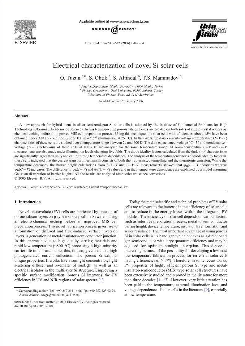
temperature increases the ideality factor n decreases whereas
the /B0 increases (n = 19.656 and /B0=0.164 eV at 79 K,
n =3.441 and /B0=0.787 eV at 400 K), in agreement with
published literature [22]. The behaviour of the diode ideality
factor n given above suggests that the current transport
mechanism consists of both the trap-assisted tunnelling and
the thermionic emission [19].
The barrier height values /B( I – V ) calculated from I – V
characteristics increase whereas the barrier height values
/B(C – V ) determined from C À2 vs. V plot (at 100 kHz)
decrease linearly with increasing of temperature (Fig. 5). It is
suggested by Rhoderick and Williams [19] that the C – V
method yields the flat band barrier height but the I – V method
gives the zero-bias barrier height, which may be lower than the
flat band value due to image force barrier lowering. This
difference, however, is considered small relative to the possible
effects of an insulating layer or of charges existing at thesemiconductor– metal interface.
While the zero-bias barrier height /B0 increases, the ideality
factor n decreases with an increased in temperature; these
changes become more significant at low temperatures (165
K) due to the large leakage current.
3.2.1. Inhomogeneous barrier analysis
The difference between /B( I – V ) and /B(C – V ) has been
explained by assumption of a Gaussian distribution of barrier
heights with a mean value /B and standard deviation rs which
can be given as [31–38]
P /Bð Þ ¼ 1
rs
ffiffiffiffiffiffi2k
p expÀ /
B0 À /B
À Á2
2r2s
" #ð4Þ
where 1=rs
ffiffiffiffiffiffi2k
p is the normalization constant.
The total current I (V ) can be calculated by integrating the
current determined by the ideal thermionic emission (TE)
model for a single barrier height and weighted by the
distribution function [33–37]. The current I (V ) expression
through a Schottky barrier at a forward bias has similar
forms as Eqs. (1) and (2) but with the modified barrier
height [38]:
I V ð Þ ¼ AA4T 2exp À q
kT ¯ /B À qr2
s
2kT
!exp
q V À I Rsð ÞnapkT
!
 1 À exp À q
kT V À IRsð Þ
n oð5Þ
with
I 0 ¼ AA4
T
2
exp
q
kT /ap ð6Þ
where /ap and nap are the apparent barrier height and
apparent ideality factor, respectively, and are given by
/B I À V ð Þ ¼ ¯ /B T ð Þ À qr2s
2kT ð7Þ
The I – V characteristics at low temperatures can still be
described by Eqs. (1) and (2). Moreover, it has been
demonstrated that the capacitance depends only on the mean
barrier height and /B(C ÀV ) is equal to the mean barrier height
/ B [31–34],
/B C À V ð Þ ¼ ¯ /B T ð Þ ð8Þ
Table 1
Temperature dependence of various parameters determined from I – V
characteristics of novel Si solar cell
T (K) I 0 (A) n /B( I ÀV ) (eV)
79 1.938Â10À5 19.656 0.164
125 2.037Â10À5 11.297 0.268
165 4.377Â10
À5
8.860 0.351205 9.963Â10À5 7.380 0.429
250 1.498Â10À4 5.560 0.523
300 2.086Â10À4 4.400 0.628
325 2.814Â10À4 3.806 0.677
350 4.774Â10À4 3.532 0.718
373 8.625Â10À4 3.448 0.750
400 1.635Â10À3 3.411 0.787
n(T) = 1613/T - 0.972
2
4
6
8
10
12
14
16
18
20
0 4 8 10 12 14
n
1000/T (K-1)
2 6
Fig. 4. Plot of n vs. 1000/ T of novel Si solar cell in dark.
ΦB(C-V) = -0.0008T + 1.1339
ΦB0(I-V) = 0.0019T + 0.0225
0.00
0.30
0.60
0.90
1.20
0 75 150 225 300 375 450
T (K)
Φ B ( e V )
Fig. 5. Zero-bias barrier height /B0( I ÀV ) (open circles) from I – V data and the
/B
(C À
V ) (filled circles) from C – V data as a function of the temperature.
O. Tuzun et al. / Thin Solid Films 511–512 (2006) 258–264 261
Page 5
7/28/2019 1-s2.0-S0040609005024570-main
http://slidepdf.com/reader/full/1-s20-s0040609005024570-main 5/7
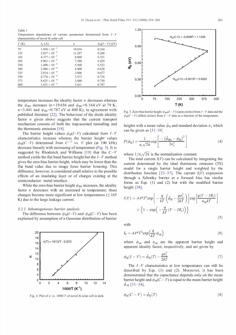
Comparing Eqs. (7) and (8), one gets
/B C À V ð Þ À /B I À V ð Þ ¼ qr2s
2kT ,
qr2s0
2kT þ qrs0ar
k ð9Þ
The plot of /B(C ÀV )À/B( I ÀV ) as a function of T À1
shows almost linear relationship at temperatures above 165 K
(Fig. 6). The values of rs0=162 meV and ar =0.268 meV K
are calculated from the slope and intercept, respectively. The
conventional Richardson plot is now modified as [25,31–34]
ln I 0=T 2
À ÁÀ q2r2
s0
2k 2T 2¼ ln AA4eÀ qa/=k ð Þ
À q¯ /B0
kT ð10Þ
Using the rs0 value derived from Fig. 6, values for ln I 0=T 2ð Þ À q2r2
s0
2k 2T 2
are calculated and plotted as a function
of T À1 in Fig. 7. The plot of Ln( I 0 / T 2) as a function of
T À1 is also given in the same figure for comparison.
By least square linear fitting, the value found from the slope
for /B0 is 0.830 eV which is in a good agreement with the
room temperature /B(C ÀV ) value of 0.889 eV. The value of
A* obtained from the intercept of /B(C ÀV ) vs. T plot is about
A*=24.79 A cmÀ2 K À2 which is in a fairly good agreement
with the theoretical value of 32 A cmÀ2 K À2.
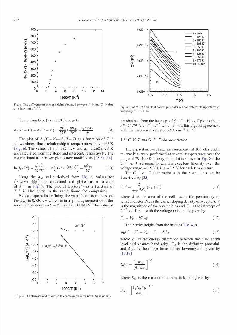
3.3. C–V–T and G–V–T characteristics
The capacitance–voltage measurements at 100 kHz under
reverse bias were performed at several temperatures over the
range of 79–400 K. The typical plot is shown in Fig. 8. The
C À2 vs. V relationship exhibits excellent linearity over the
voltage range À0.5 VV À2.5 V for each temperature.
The C À2 vs. V characteristics in these structures can be
described by [35]
C À2 ¼ 2
qes A2 N AV 0 þ V ð Þ ð11Þ
where A is the area of the cells, (s is the permittivity of
semiconductor, N A is the carrier doping density of acceptors, V
is the magnitude of the reverse bias and V 0 is the intercept of
C À2 vs. V plot with the voltage axis and is given by
V 0 ¼ V D À kT =q ð12ÞThe barrier height from the inset of Fig. 8 is
/B C
ÀV
ð Þ ¼V D
þ E F
ÀD/B
ð13
Þwhere E F is the energy difference between the bulk Fermi
level and valance band edge, V D is the diffusion potential,
and D/B is the image force barrier lowering and given by
[18,19]
D/B ¼ qE m
4kese0
!1=2
ð14Þ
where E m is the maximum electric field and given by
E m¼
2qN AV D
ese0 !
1=2
ð15
Þ
0
100
200
300
400
500
600
700
800
900
0 4 8 10 12 14
1000/T (K-1)
2 6
Φ B ( C - V ) -Φ B 0 ( I - V ) ( m e V )
Fig. 6. The difference in barrier heights obtained between I – V and C – V data
as a function of 1/ T .
-55
-50
-45
-40
-35
-30
-25
-20
-15
-10
0 2 6 7
L n ( I o
/ T 2 ) ( A K - 2 )
Ln(Io /T2)
Ln(Io /T2)-(q2
σ2 /2k2T2)
1000/T (K-1)
1 3 4 5
Fig. 7. The standard and modified Richardson plots for novel Si solar cell.
1.0E+14
2.0E+14
3.0E+14
4.0E+14
5.0E+14
-2.5 -1.5 -0.5 0.5 1.5
V (V)
C - 2 ( F
- 2 )
1
10
1 - 79 K
2 - 125 K
3 - 165 K4 - 205 K
5 - 250 K
6 - 300 K
7 - 325 K8 - 350 K
9 - 373 K
10 - 400 K
Fig. 8. Plot of 1/ C 2 vs. V of porous p-Si solar cell for different temperatures at
frequency of 100 kHz.
O. Tuzun et al. / Thin Solid Films 511– 512 (2006) 258 –264262
Page 6
7/28/2019 1-s2.0-S0040609005024570-main
http://slidepdf.com/reader/full/1-s20-s0040609005024570-main 6/7
The temperature variation of /B(C ÀV ) can be readily
calculated with the use of following standard relations [19],
E F ¼ kT
qln N V= N Að Þ ð16aÞ
with
N V ¼ 4:82 Â 1015T 3=2 mh=m0ð Þ3=2; mh=m0ð Þ ¼ 0:55 ð16bÞwhere N V is the effective density of states in Si valance band,
mh is the effective mass of holes and m0 is the rest mass of the
electron.
The values of N A, E F, V D, W D, and D/B determined from
C À2 vs. V curves at different temperatures are listed in Table 2.
We found from the measurement C – V data, the barrier height
/B(C ÀV ) decreases almost linearly with temperature as
/B C À V ð Þ ¼ /B0 þ a/T ð17ÞHere the barrier height at absolute zero /B0 and temperature
coefficient of the barrier height a/ are experimentally found to be 1.13 eV and 8Â10À4 eV/K, respectively. The negative
temperature coefficient of the barrier height is found to be very
close of the Si band gap (¨4.73Â10À4 eV/K). Similar a-
values of 2–10Â10À4 eV/K have been reported [22,24,29].
3.3.1. Temperature and voltage dependent series resistance
The C – V and G – V measurements at 100 kHz were
performed at different temperatures at the range of 79– 400 K.
In addition, the room temperature C – V and G – V measurements
at 100 kHz were made at the different illumination levels. Before
any analysis could take place, all the measurements must be
corrected for series resistance because the series resistance is avery important parameter of solar cells. Therefore, the values of
Rs are calculated from the measured admittance when the solar
cells are biased in strong accumulation [11,21,28,36]. In
addition to voltage dependence of the series resistance can be
obtained from the measurements of C – V and G – V curves,
according to [28,37]
Rs ¼ G ma
G 2ma þ xC mað Þ2ð18Þ
where C ma and G ma represent the measured capacitance and
conductance values, respectively, in strong accumulation region.
All the measured capacitance and conductance values were
corrected using calculated series resistance [28]
C c ¼G 2m þ xC mð Þ2h i
C m
a2 þ xC mð Þ2and
G c ¼ G 2m þ xC mð Þ2a
a2 þ xC mð Þ2ð19Þ
where
a
¼C m
À)G 2m
þxC m
ð Þ22 Rs
ð20
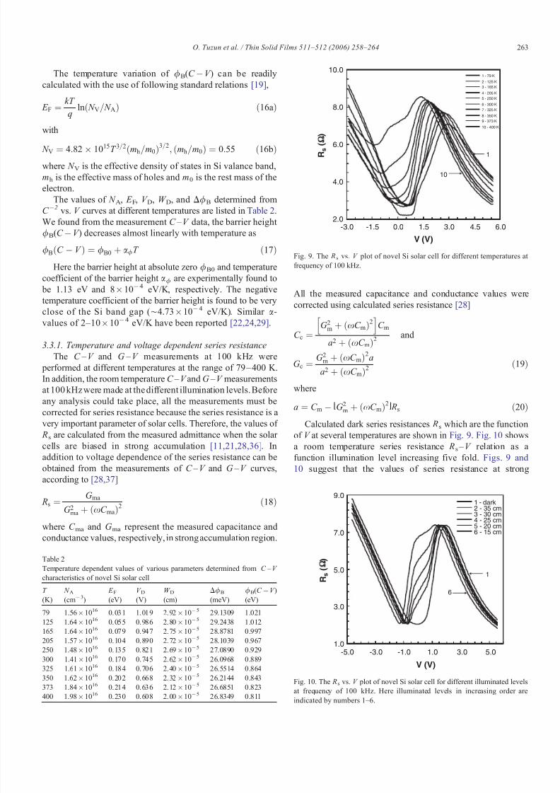
ÞCalculated dark series resistances Rs which are the function
of V at several temperatures are shown in Fig. 9. Fig. 10 shows
a room temperature series resistance Rs – V relation as a
function illumination level increasing five fold. Figs. 9 and
10 suggest that the values of series resistance at strong
Table 2
Temperature dependent values of various parameters determined from C – V
characteristics of novel Si solar cell
T
(K)
N A(cmÀ3)
E F(eV)
V D(V)
W D(cm)
D/B
(meV)
/B(C ÀV )
(eV)
79 1.56Â1016 0.031 1.019 2.92Â10À5 29.1309 1.021
125 1.64Â1016 0.055 0.986 2.80Â10À5 29.2438 1.012
165 1.64Â1016 0.079 0.947 2.75Â10À5 28.8781 0.997
205 1.57Â1016 0.104 0.890 2.72Â10À5 28.1039 0.967
250 1.48Â1016 0.135 0.821 2.69Â10À5 27.0890 0.929
300 1.41Â1016 0.170 0.745 2.62Â10À5 26.0968 0.889
325 1.61Â1016 0.184 0.706 2.40Â10À5 26.5514 0.864
350 1.62Â1016 0.202 0.668 2.32Â10À5 26.2144 0.843
373 1.84
Â1016 0.214 0.636 2.12
Â10À5 26.6851 0.823
400 1.98Â1016 0.230 0.608 2.00Â10À5 26.8349 0.811
2.0
4.0
6.0
8.0
10.0
-3.0 -1.5 0.0 1.5 3.0 4.5 6.0
V (V)
R s
(Ω )
1
10
1 - 79 K
2 - 125 K
3 - 165 K
4 - 205 K
5 - 250 K
6 - 300 K
7 - 325 K
8 - 350 K
9 - 373 K
10 - 400 K
Fig. 9. The Rs vs. V plot of novel Si solar cell for different temperatures at
frequency of 100 kHz.
1.0
3.0
5.0
7.0
9.0
-5.0 -3.0 -1.0 1.0 3.0 5.0
1 - dark2 - 35 cm3 - 30 cm4 - 25 cm5 - 20 cm6 - 15 cm
V (V)
1
6
R s
(Ω )
Fig. 10. The Rs vs. V plot of novel Si solar cell for different illuminated levels
at frequency of 100 kHz. Here illuminated levels in increasing order areindicated by numbers 1–6.
O. Tuzun et al. / Thin Solid Films 511–512 (2006) 258–264 263
Page 7
7/28/2019 1-s2.0-S0040609005024570-main
http://slidepdf.com/reader/full/1-s20-s0040609005024570-main 7/7
accumulation (5.5 V) decrease with increasing temperature and
illumination level. However, the series resistance values for
both in dark and under illumination change from region to
region with applied voltage. Especially, while the values of
series resistance decrease with increasing temperature in
accumulation region, and increase with increasing temperature
in depletion and reverse regions. The values of Rs becomemaximum at about between 1 VV 3.5 V. These peaks
shifted to accumulation region with decreasing temperature and
amplitude of peaks increased with increasing temperature in the
dark C – V and G – V measurements, but under illumination
these peaks almost remain constant. Such behaviour of the
series resistance has been attributed to particular distribution of
interface states [19,36]. As shown in Figs. 9 and 10, the values
of series resistance showed a strong dependence on the applied
voltage at various temperatures and illumination levels.
4. Conclusion
In analysis of the novel photovoltaic cells fabricated by
creation of porous silicon layers on p-type monocrystalline Si
wafers using an electro-chemical etching before an improved
MIS cell preparation process, it is found that the ideality factor
n, series resistance Rs and barrier height /B were strongly
dependent on temperature. While the ideality factor n and
series resistance Rs decrease, the zero-bias barrier heights /B0
increase with increasing temperature. A disagreement between
the barrier height calculated from C – V measurements and
those determined from I – V data could be explained by
assuming a Gaussian distribution of barrier heights. In other
words, the discrepancy between barrier heights deduced from
the I – V and C – V measurements is thought to be a result of domination of low current level through a lower barrier where
the /B( I ÀV ) calculations carried out. Moreover, the value of
the Richardson constant was found to be 24.79 A K À2 cmÀ2,
which is very close to the theoretical value of 32 A K À2 cmÀ2
used for the determination of the zero-bias barrier height.
We observed that from the admittance measurements (C – V
and G – V ), the increase of capacitance C and conductance G
under illumination are due to the formation of an inversion
layer at semiconductor– insulator interface. Both excess capac-
itance and excess conductance under illumination are thought
to be the results of both the change at interface states response
and the solar cell series resistance.
Acknowledgements
The authors acknowledge the supports given by NATO
(project no SfP 971829), TUBITAK-Marmara Research Centre
(Turkey), Institute of Fundamental Problems for High Tech-
nology, Ukrainian Academy of Sciences and Gazi University
Physics Laboratories (Turkey).
References
[1] M. Tiris, V. Kochelap, N. Syred, J. Knobloch, Research and Demonstra-
tion of Advanced Silicon PV Technology for Terrestrial Applications in
Ukraine, NATO (project no SfP 971829) Progress Report-V, May 2003.
[2] J. Shewchun, D. Burk, M.B. Spitzer, IEEE Trans. Electron Devices ED-27
(1980) 705.
[3] R.N. Hall, Solid-State Electron. 24 (1981) 595.[4] M. Wolf, G.T. Noel, R.J. Stirn, IEEE Trans. Electron Devices ED-24
(1977) 419.
[5] S. Ozdemir, U. Buget, O. Oktu, Sol. Cells 20 (1987) 81.
[6] J.P. Ponpon, P. Siffert, J. Appl. Physi. 47 (1976) 3248.
[7] S. Biswas, A. Mansingh, J. Phys. D: Appl. Phys. 25 (1992) 100.
[8] E. Badura, W. Zdanowicz, Sol. Energy Mater. 4 (1980) 81.
[9] W.M.R. Divigalpitiya, Sol. Energy Mater. 18 (1989) 253.
[10] S. Ozdemir, S. Alt Nndal, Sol. Energy Mater. Sol. Cells 32 (1994) 115.
[11] S. Alt Nndal, A. Tataroglu, I. Dokme, Sol. Energy Mater. Sol. Cells 85
(2005) 345.
[12] W.A. Anderson, J.K. Kim, A.E. Delahoy, IEEE Trans. Electron Devices
ED-24 (1977) 453.
[13] P. Vitanov, M. Kamenova, N. Tyutyundzhiev, M. Delibasheva, E.
Goranova, M. Peneva, Thin Solid Films 297 (1997) 299.
[14] B. Unal, S.C. Bayliss, J. Phys. D: Appl. Phys. 30 (1997) 2763.
[15] M. Tucci, M. della Noce, E. Bobeico, F. Roca, G. de Cesare, F. Palma,
Thin Solid Films 451–452 (2004) 355.
[16] R. Brendel, K. Feldrapp, R. Horbelt, R. Auger, Phys. Status Solidi, A
Appl. Res. 197 (2003) 497.
[17] V.Y. Yerokhov, R. Henzel, M. Lipinski, R. Ciach, H. Nagel, A.
Mylyanych, P. Panek, Sol. Energy Mater. Sol. Cells 72 (2002) 291.
[18] S.M. Sze, Physics of Semiconductor Devices, 2nd Ed., John Wiley &
Sons, New York, 1981.
[19] E.H. Rhoderick, R.H. Williams, Metal Semiconductor Contacts, 2nd edR,
Clarendon Press, Oxford, 1988.
[20] H.J. Hovel, Semiconductor and Semimetals, Solar Cells, vol. 11,
Academic Press, New York, 1975.
[21] N. Konofaos, I.P. McClean, C.B. Thomas, Phys. Status Solidi, A Appl.
Res. 161 (1997) 111.
[22] S. Alt Nndal, S. Karadeniz, N. Tugluoglu, A. Tataroglu, Solid-State
Electron. 47 (2003) 1847.
[23] P. Cova, A. Singh, J. Appl. Physi. 82 (10) (1997) 5217.
[24] A. Singh, K.C. Reinhart, W.A. Anderson, J. Appl. Phys. 68 (7) (1990)
3475.
[25] S. Chand, J. Kumar, Appl. Phys. A 63 (1996) 171.
[26] D.B. Dimitrov, Phys. Rev., B, Condens. Matter 51 (1995) 1562.
[27] H.C. Card, E.H. Rhoderick, J. Phys. D 4 (1971) 1589.
[28] E.H. Nicollian, J.R. Brews, Metal Oxide Semiconductor (MOS) Physics
and Technology, Wiley, New York, 1982.
[29] P. Cova, A. Singh, Solid-State Electron. 33 (1990) 11.
[30] B. Akkal, Z. Benamara, B. Gruzza, L. Bideux, Vacuum 57 (2000) 219.
[31] Y.P. Song, R.L. Van Meirhaeghe, W.H. Laflere, F. Cardon, Solid-State
Electron. 29 (1986) 633.
[32] S. Zhu, C. Detavernier, R.L. Van Meirhaeghe, F. Cardon, G.P. Ru, X.P.
Qu, B.Z. Li, Solid-State Electron. 44 (2000) 1807.
[33] J.H. Werner, H.H. Gut tler, J. Appl. Phys. 69 (1991) 1522.
[34] J.H. Werner, H.H. Gut tler, Phys. Scr. T39 (1991) 258.
[35] J. Shewchun, M.A. Green, F.D. King, Solid-State Electronics 17 (1974)
563.
[36] A. Singh, Solid-State Electron. 28 (1985) 223.
[37] A. Tataroglu, S. Alt Nndal, S. Karadeniz, N. Tugluoglu, Microelectron. J.
34 (2003) 1043.
[38] S. Zhu, R.L. Van Meirhaeghe, C. Detavernier, F. Cardon, G.P. Ru, X.P.
Qu, B.Z. Li, Solid-State Electron. 44 (2000) 663.
O. Tuzun et al. / Thin Solid Films 511– 512 (2006) 258 –264264