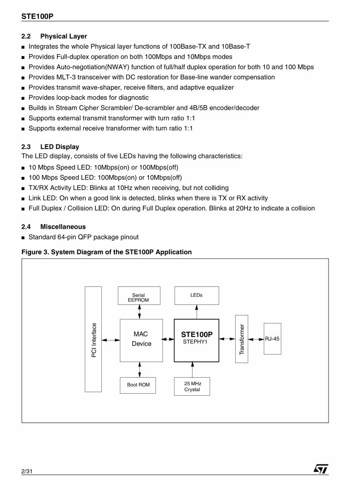
1/31 STE100P February 2006 1 DESCRIPTION The STE100P, also referred to as STEPHY1, is a high performance Fast Ethernet physical layer in- terface for 10Base-T and 100Base-TX applica- tions. It was designed with advanced CMOS technology to provide a Media Independent Interface (MII) for easy attachment to 10/100 Media Access Control- lers (MAC) and a physical media interface for 100Base-TX of IEEE802.3u and 10Base-T of IEEE802.3. The STEPHY1 supports both half-duplex and full- duplex operation, at 10 and 100 Mbps operation. Its operating mode can be set using auto-negotia- tion, parallel detection or manual control. It also al- lows for the support of auto-negotiation functions for speed and duplex detection. 2 FEATURES 2.1 Industry standard ■ IEEE802.3u 100Base-TX and IEEE802.3 10Base-T compliant ■ Support for IEEE802.3x flow control ■ IEEE802.3u Auto-Negotiation support for 10Base-T and 100Base-TX ■ MII interface ■ Standard CSMA/CD or full duplex operation supported ■ Industrial temperature compliant 10/100 FAST ETHERNET 3.3V TRANSCEIVER Figure 2. Block Diagram NRZ To Manchester Encoder MII Interface / Controller 10 TX Filter TRANSMITTER 10/100 Scrambler Auto Negotiation 4B/5B NRZ To NRZI Encoder Link Pulse Generator Binary To MLT3 Encoder RECEIVER 10/100 Parallel to Serial Descrambler Code Align 4B/5B NRZI To NRZ Decoder Serial to Parallel NRZ To Manchester Encoder Link Pulse Detector SMART Squelch 10 TX Filter Clock Recovery Clock Generation System Clock Adaptive Equalization BaseLine Wander Binary To MLT3 Decoder Clock Recovery REGISTERS HW Config Power Down LEDS RX Channel TX Channel TXP TXN RXP RXN MDC MDIO RXD[3:0] RX_ER RX_DV RX_CLK TX_CLK TXD[3:0] TX_ER TX_EN LEDS HW configuration pins Serial Management 10Mb/s 100Mb/s 100Mb/s 10Mb/s Loopback Rev. 19 Figure 1. Package Table 1. Order Codes (*) ECOPACK® (see Section 9) Part Number Package STE100P TQFP64 E-STE100P (*) TQFP64 TQFP64 (10x10x1.40mm)
Transcript
1/31
STE100P
February 2006
1 DESCRIPTIONThe STE100P, also referred to as STEPHY1, is ahigh performance Fast Ethernet physical layer in-terface for 10Base-T and 100Base-TX applica-tions.It was designed with advanced CMOS technologyto provide a Media Independent Interface (MII) foreasy attachment to 10/100 Media Access Control-lers (MAC) and a physical media interface for100Base-TX of IEEE802.3u and 10Base-T ofIEEE802.3. The STEPHY1 supports both half-duplex and full-duplex operation, at 10 and 100 Mbps operation.Its operating mode can be set using auto-negotia-tion, parallel detection or manual control. It also al-lows for the support of auto-negotiation functionsfor speed and duplex detection.
2 FEATURES
2.1 Industry standard IEEE802.3u 100Base-TX and IEEE802.3
10Base-T compliant
Support for IEEE802.3x flow control IEEE802.3u Auto-Negotiation support for
10Base-T and 100Base-TX MII interface Standard CSMA/CD or full duplex operation
supported Industrial temperature compliant
10/100 FAST ETHERNET 3.3V TRANSCEIVER
Figure 2. Block Diagram
NRZ To ManchesterEncoder
MII
Inte
rface
/ C
ontr
olle
r
10 TXFilter
TRANSMITTER10/100
Scrambler
AutoNegotiation
4B/5B NRZ To NRZI Encoder
Link PulseGenerator
Binary To MLT3Encoder
RECEIVER10/100
Parallel toSerial
DescramblerCode Align4B/5B NRZI To NRZ
DecoderSerial toParallel
NRZ To ManchesterEncoder
Link PulseDetector
SMARTSquelch
10 TX Filter
Clock Recovery
ClockGeneration
SystemClock
AdaptiveEqualization
BaseLineWander
Binary To MLT3Decoder
Clock Recovery
REGISTERS
HW ConfigPower Down
LEDS
RX Channel
TX Channel
TXP
TXN
RXP
RXN
MDC
MDIO
RXD[3:0]
RX_ER
RX_DV
RX_CLK
TX_CLK
TXD[3:0]
TX_ER
TX_EN
LEDS
HW configuration pins
Ser
ial M
anag
emen
t
10Mb/s
100Mb/s
100Mb/s
10Mb/s
Loopback
Rev. 19
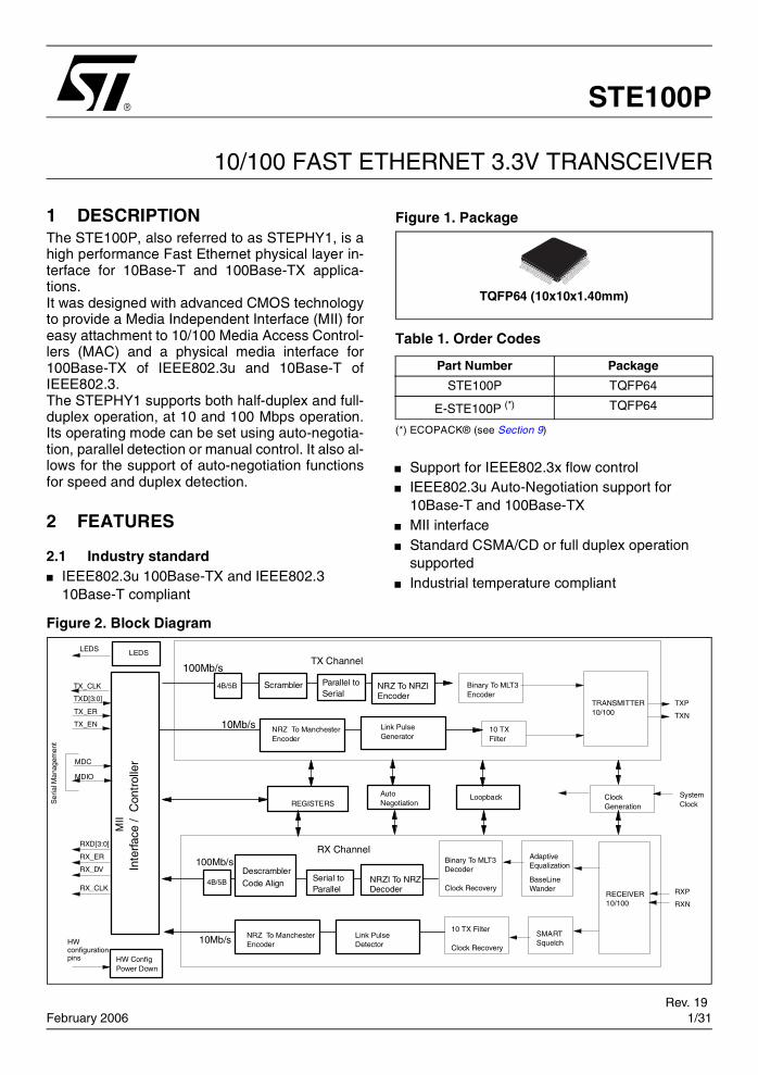
Figure 1. Package
Table 1. Order Codes
(*) ECOPACK® (see Section 9)
Part Number Package
STE100P TQFP64
E-STE100P (*) TQFP64
TQFP64 (10x10x1.40mm)
STE100P
2/31
2.2 Physical Layer
Integrates the whole Physical layer functions of 100Base-TX and 10Base-T
Provides Full-duplex operation on both 100Mbps and 10Mbps modes
Provides Auto-negotiation(NWAY) function of full/half duplex operation for both 10 and 100 Mbps
Provides MLT-3 transceiver with DC restoration for Base-line wander compensation
Provides transmit wave-shaper, receive filters, and adaptive equalizer
Provides loop-back modes for diagnostic
Builds in Stream Cipher Scrambler/ De-scrambler and 4B/5B encoder/decoder
Supports external transmit transformer with turn ratio 1:1
Supports external receive transformer with turn ratio 1:1
2.3 LED DisplayThe LED display, consists of five LEDs having the following characteristics:
10 Mbps Speed LED: 10Mbps(on) or 100Mbps(off)
100 Mbps Speed LED: 100Mbps(on) or 10Mbps(off)
TX/RX Activity LED: Blinks at 10Hz when receiving, but not colliding
Link LED: On when a good link is detected, blinks when there is TX or RX activity
Full Duplex / Collision LED: On during Full Duplex operation. Blinks at 20Hz to indicate a collision
2.4 Miscellaneous
Standard 64-pin QFP package pinout
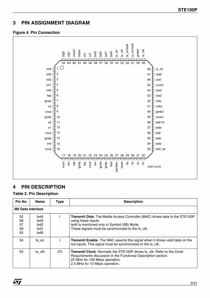
Figure 3. System Diagram of the STE100P Application
Boot ROM 25 MHzCrystal
RJ-45STE100PSTEPHY1
SerialEEPROM
LEDs
PC
I Int
erfa
ce
MAC
Device
Transf
orm
er
3/31
STE100P
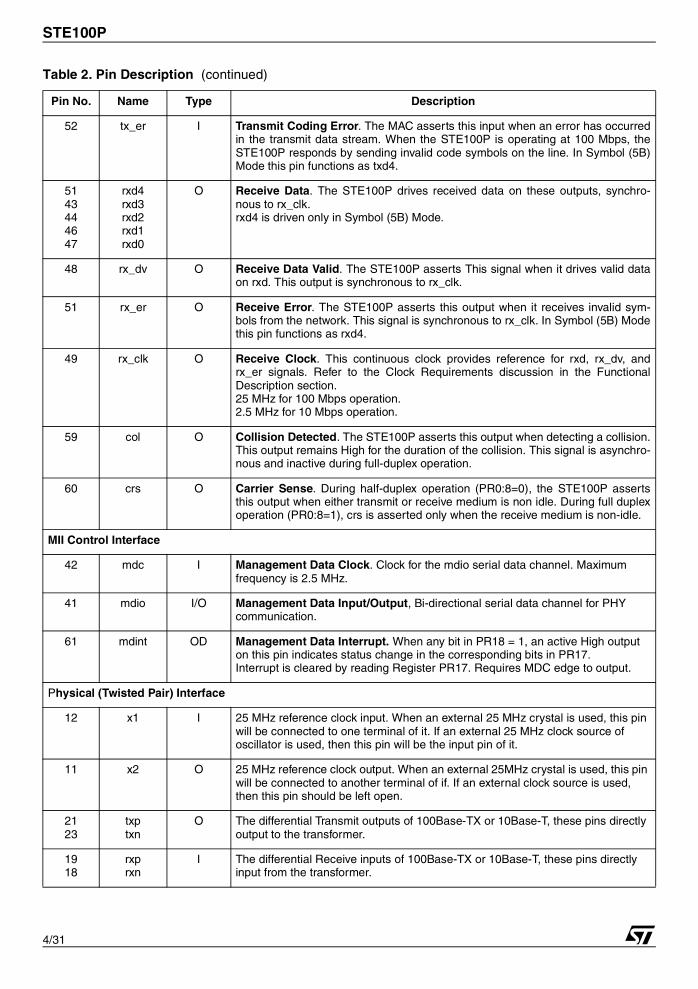
3 PIN ASSIGNMENT DIAGRAM
Figure 4. Pin Connection
4 PIN DESCRIPTIONTable 2. Pin Description
Pin No. Name Type Description
MII Data Interface
5258575655
txd4txd3txd2txd1txd0
I Transmit Data. The Media Access Controller (MAC) drives data to the STE100P using these inputs. txd4 is monitored only in Symbol (5B) Mode. These signals must be synchronized to the tx_clk.
54 tx_en I Transmit Enable. The MAC asserts this signal when it drives valid data on the txd inputs. This signal must be synchronized to the tx_clk.
53 tx_clk I/O Transmit Clock. Normally the STE100P drives tx_clk. Refer to the Clock Requirements discussion in the Functional Description section.25 MHz for 100 Mbps operation.2.5 MHz for 10 Mbps operation.
1
2
3
5
6
4
7
8
9
10
27
11
28 29 30 31 32
59 58 57 56 5455 53 52 51 50 49
43
42
41
39
38
40
48
47
46
44
45
fde
mf0
mf1
mf3
mf4
mf2
x2
gnda
vcca
gnda
nc
vcca txn
gnda
gnde
pwrd
wn
test
rese
t
rip nc nc nc
col
txd3
txd2
txd1
tx_e
n
txd0
tx_c
lk
tx_e
r/tx
d4
rx_e
r/rx
d4
gnde
/i
rx_c
lk
rdx3
mdc
mdio
vcce/i
ledr10
gnde/i
rx_dv
rxd0
rxd1
rdx2
vcce/i
D99TL457B
22 23 24 25 26
60
crs
61
mdi
nt
62
vcce
/i
63
cfg1
64cf
g0vc
ca rxn
rxp
gnda tx
p
17 18 19 20 21
37
36
34
33
35
ledtr
ledl
leds
test_se
ledc
12
13
14
15
16vcca
iref
gnda
x1
vcca
STE100P
4/31
52 tx_er I Transmit Coding Error. The MAC asserts this input when an error has occurredin the transmit data stream. When the STE100P is operating at 100 Mbps, theSTE100P responds by sending invalid code symbols on the line. In Symbol (5B)Mode this pin functions as txd4.
5143444647
rxd4rxd3rxd2rxd1rxd0
O Receive Data. The STE100P drives received data on these outputs, synchro-nous to rx_clk.rxd4 is driven only in Symbol (5B) Mode.
48 rx_dv O Receive Data Valid. The STE100P asserts This signal when it drives valid dataon rxd. This output is synchronous to rx_clk.
51 rx_er O Receive Error. The STE100P asserts this output when it receives invalid sym-bols from the network. This signal is synchronous to rx_clk. In Symbol (5B) Modethis pin functions as rxd4.
49 rx_clk O Receive Clock. This continuous clock provides reference for rxd, rx_dv, andrx_er signals. Refer to the Clock Requirements discussion in the FunctionalDescription section.25 MHz for 100 Mbps operation.2.5 MHz for 10 Mbps operation.
59 col O Collision Detected. The STE100P asserts this output when detecting a collision.This output remains High for the duration of the collision. This signal is asynchro-nous and inactive during full-duplex operation.
60 crs O Carrier Sense. During half-duplex operation (PR0:8=0), the STE100P assertsthis output when either transmit or receive medium is non idle. During full duplexoperation (PR0:8=1), crs is asserted only when the receive medium is non-idle.
MII Control Interface
42 mdc I Management Data Clock. Clock for the mdio serial data channel. Maximum frequency is 2.5 MHz.
41 mdio I/O Management Data Input/Output, Bi-directional serial data channel for PHY communication.
61 mdint OD Management Data Interrupt. When any bit in PR18 = 1, an active High output on this pin indicates status change in the corresponding bits in PR17.Interrupt is cleared by reading Register PR17. Requires MDC edge to output.
Physical (Twisted Pair) Interface
12 x1 I 25 MHz reference clock input. When an external 25 MHz crystal is used, this pin will be connected to one terminal of it. If an external 25 MHz clock source of oscillator is used, then this pin will be the input pin of it.
11 x2 O 25 MHz reference clock output. When an external 25MHz crystal is used, this pin will be connected to another terminal of if. If an external clock source is used, then this pin should be left open.
2123
txptxn
O The differential Transmit outputs of 100Base-TX or 10Base-T, these pins directly output to the transformer.
1918
rxp rxn
I The differential Receive inputs of 100Base-TX or 10Base-T, these pins directly input from the transformer.
Table 2. Pin Description (continued)
Pin No. Name Type Description
5/31
STE100P
15 iref O Reference Resistor connecting pin for reference current, directly connect a 5KΩ ± 1% resistor to Vss.
38 ledr10 I/O LED display for 10Ms/s link status. This pin will be driven on continually when 10Mb/s network operating speed is detected.The pull-up/pull-down status of this pin is latched into the PR20 bit 7 during power up/reset.
37 ledtr LED display for Tx/Rx Activity status. This pin will be driven on at a 10 Hz blinking frequency when either effective receiving or transmitting is detected.The status of this pin is latched into the PR20 bit 6 during power up/reset.
36 ledl I/O LED display for Link Status. Blinks when there is TX or RX activity. This pin will be driven on continually when a good Link test is detected. The status of this pin is latched into the PR20 bit 5 during power up/reset.
35 ledc I/O LED display for Full Duplex or Collision status. This pin will be driven on continually when a full duplex configuration is detected. This pin will be driven on at a 20 Hz blinking frequency when a collision status is detected in the half duplex configuration.The status of this pin is latched into the PR20 bit 4 during power up/reset.
34 leds I/O LED display for 100Ms/s link status. This pin will be driven on continually when 100Mb/s network operating speed is detected.The status of this pin is latched into the PR20 bit 3 during power up/reset.
64 cfg0 I Configuration Control 0.When A/N is enabled, cfg0 determines operating mode advertisement capabilities in combination with cfg1 when mf0/ PR0:12 =1. (See Table 2)When A/N is disabled, cfg1 disables mlt3 and directly affects PR19:0When cfg0 is Low, mlt3 encoder/decoder is enabled and PR19:1 =0. When cfg0 is High, mlt3 encoder/decoder is bypassed and PR19:1 = 1.
63 cfg1 I Configuration Control 1.When A/N is enabled, cfg1 determines operating mode advertisement capabilities in combination with cfg1 when mf0/ PR0:12 =1. (See Table 2)When A/N is disabled, CFG1 enables Loopback mode and directly affects PR0 bit 14.When cfg1 is Low, Loopback mode is disabled and PR0:14 = 0.When cfg1 is High, Loopback mode is enabled and PR0:14 = 1.
28 reset I Reset (Active-Low). This input must be held low for a minimum of 1 ms to reset the STE100P. During Power-up, the STE100P will be reset regardless of the state of this pin, and this reset will not be complete until after >1ms.
29 rip O Reset In Progress. This output is used to indicate when the device has completed power-up/reset and the registers and functions can be accessed.When rip is High, power-up/reset has been successful and the device can be used normallyWhen rip is Low, device reset is not complete.
8, 30,31,32
nc nc (No Connection)
26, 33 test, test_se
Test pins. Should be tied to ground for normal operation
27 pwrdwn I Power Down. When High, forces STE100P into Power Down mode. This pin is OR’ed with the Power Down bit (PR0:11). During the Power Down mode, txp/txn outputs and all LED outputs are 3-stated, and the MII interface is isolated.
Table 2. Pin Description (continued)
Pin No. Name Type Description
STE100P
6/31
54321
mf0mf1mf2mf3mf4
I Multi-Function pins. Each mf pin internally drives different configuration functions. The functions of the five mf inputs are as shown in the table below.
The logic level of mf0-4 will determine the value that the affected bits will have upon reset of the STE100P. The operating functions of cfg0, cfg1, and fde change depending on the state of mf0 (Auto-Negotiation enabled or disabled). Table 2 shows the relationship between cfg0, cfg1 and fde.
6 fde I Full-Duplex Enable. When A/N is enabled, fde determines full-duplex advertisement capability in combination with cfg0 and cfg1. (See Table 2)When A/N is disabled, fde directly affects full-duplex operation and determines the value of PR0 bit 8 (Full/Half Duplex Mode Select).When fde is High, full-duplex is enabled and PR0:8 = 1.When fde is Low, full-duplex is disabled and PR0:8 = 0.
Digital Power Pins
39, 45, 62 vcce, vcce/i
25, 40, 50 gnde, gnde/i
Analog Power Pins
9, 13, 16, 17, 22 vcca
7, 10, 14, 20, 24 gnda
Table 2. Pin Description (continued)
Pin No. Name Type Description
7/31
STE100P
5 HARDWARE CONTROL INTERFACE
5.1 Operating ConfigurationsThe Hardware Control Interface consists of the MF<4:0>, CFG <1:0> and FDE input pins as well as theLED/PAD pins. This interface is used to configure operating characteristics of the STE100P. The Hard-ware Control Interface provides initial values for the MDIO registers, and then passes control to the MDIOInterface. Individual chip addressing via the LED/PAD pins allows multiple STE100P devices to share theMII interface. Table 3 shows how to set up the desired operating configurations using the Hardware Con-trol Interface.
Note: If pin 5, MF0 = 0, or ANE (pin MF0 / PR0:12) = 0 (Auto-Negotiation disabled), then PR4 bits 5-8 will contain the default value indicatedin the table describing register PR4.
5.2 LED / PHY Address InterfaceThe LED output pins can be used to drive LED’s directly, or can be used to provide status information toa network management device. The active state of each LED output driver is dependent on the logic levelsampled by the corresponding PHY address input upon power-up/reset. For example, if a given PAD inputis resistively pulled low then the corresponding LED output will be configured as an active high driver. Con-versely, if a given PAD input is resistively pulled high then the corresponding LED output will be configuredas an active low driver. These outputs are standard CMOS drivers and not open-drain.
The STE100P PAD[4:0] inputs provide up to 32 unique PHY address options. An address selection of allzeros (00000) will result in a PHY isolation condition as a result of power-on/reset, as documented for PR0bit 10.
(See Section 7 for more detailed descriptions of device operation.)
Desired Configuration
Input Value PR4 Register Bits Affected
CFG0 CFG1 FDE [8] TXF [7] TXH [6] 10F [5] 10H
Advertise All 1 1 1 1 1 1 1
Advertise 100 HD 1 0 0 0 1 0 0
Advertise 100 HD/FD 1 0 1 1 1 0 0
Advertise 10 HD 0 1 0 0 0 0 1
Advertise 10 HD/FD 0 1 1 0 0 1 1
Advertise 10/100 HD 1 1 0 0 1 0 1
STE100P
8/31
6 REGISTERS AND DESCRIPTORS DESCRIPTIONThere are 11 registers with 16 bits each supported for the STE100P. These include 7 basic registers whichare defined according to the clause 22 “Reconciliation Sublayer and Media Independent Interface” andclause 28 “Physical Layer link signaling for 10 Mb/s and 100 Mb/s Auto-Negotiation on twisted pair” ofIEEE802.3u standard.
In addition, there are 4 special registers for advanced chip control and status information.
6.1 Register List
Table 4. Register List
6.2 Register Descriptions
Address Reg. Index Name Register Descriptions
0 PR0 XCR XCVR Control Register
1 PR1 XSR XCVR Status Register
2 PR2 PID1 PHY Identifier 1
3 PR3 PID2 PHY Identifier 2
4 PR4 ANA Auto-Negotiation Advertisement Register
5 PR5 ANLPA Auto-Negotiation Link Partner Ability Register
6 PR6 ANE Auto-Negotiation Expansion Register
17 PR17 XCIIS XCVR Configuration Information and Interrupt Status Register
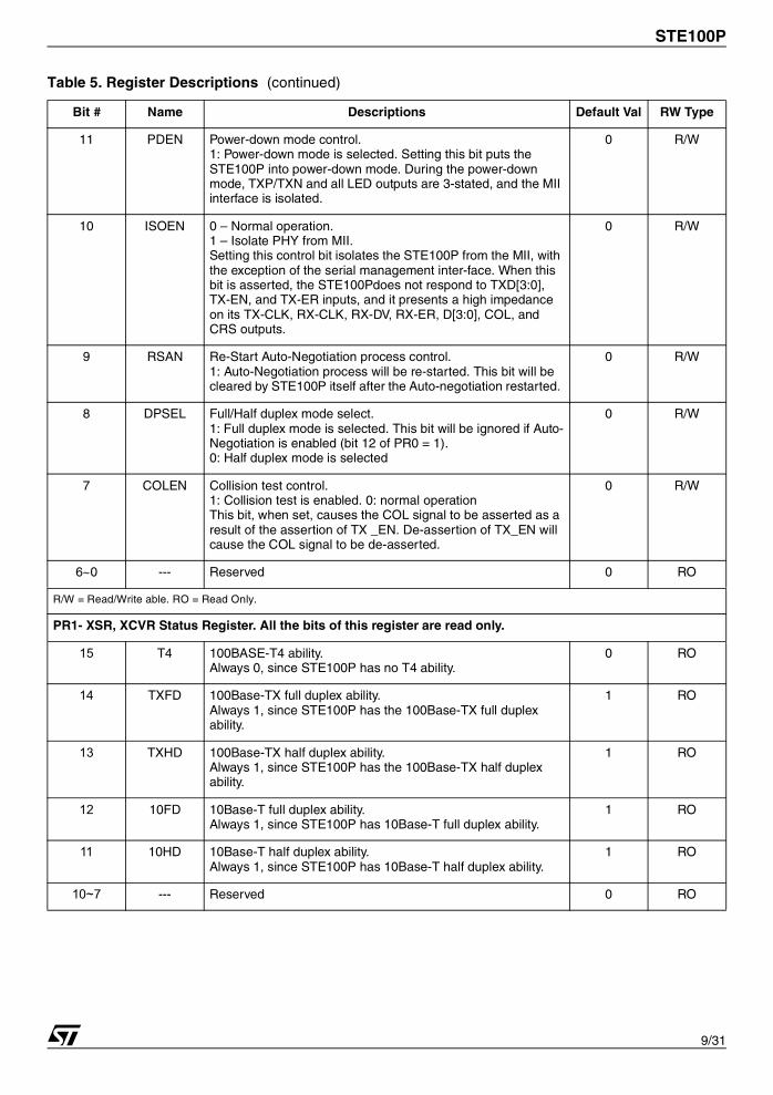
PR0- XCR, XCVR Control Register. The default values on power-up/reset are as listed below.
15 XRST Reset control. 1: Device will be reset. This bit will be cleared by STE100P itself after the reset is completed.
0 R/W
14 XLBEN Loop-back mode select. 1: Loop-back mode is selected.0: Normal mode
0 R/W
13 SPSEL Network Speed select. This bit’s selection will be ignored if Auto-Negotiation is enabled(bit 12 of PR0 = 1).1:100Mbps is selected. 0:10Mbps is selected.
1 R/W
12 ANEN Auto-Negotiation ability control. 1: Auto-Negotiation function is enabled. 0: Auto-Negotiation is disabled.
1 R/W
9/31
STE100P
11 PDEN Power-down mode control. 1: Power-down mode is selected. Setting this bit puts the STE100P into power-down mode. During the power-down mode, TXP/TXN and all LED outputs are 3-stated, and the MII interface is isolated.
0 R/W
10 ISOEN 0 – Normal operation.1 – Isolate PHY from MII.Setting this control bit isolates the STE100P from the MII, with the exception of the serial management inter-face. When this bit is asserted, the STE100Pdoes not respond to TXD[3:0], TX-EN, and TX-ER inputs, and it presents a high impedance on its TX-CLK, RX-CLK, RX-DV, RX-ER, D[3:0], COL, and CRS outputs.
0 R/W
9 RSAN Re-Start Auto-Negotiation process control. 1: Auto-Negotiation process will be re-started. This bit will be cleared by STE100P itself after the Auto-negotiation restarted.
0 R/W
8 DPSEL Full/Half duplex mode select. 1: Full duplex mode is selected. This bit will be ignored if Auto-Negotiation is enabled (bit 12 of PR0 = 1).0: Half duplex mode is selected
0 R/W
7 COLEN Collision test control. 1: Collision test is enabled. 0: normal operationThis bit, when set, causes the COL signal to be asserted as a result of the assertion of TX _EN. De-assertion of TX_EN will cause the COL signal to be de-asserted.
0 R/W
6~0 --- Reserved 0 RO
R/W = Read/Write able. RO = Read Only.
PR1- XSR, XCVR Status Register. All the bits of this register are read only.
15 T4 100BASE-T4 ability. Always 0, since STE100P has no T4 ability.
0 RO
14 TXFD 100Base-TX full duplex ability. Always 1, since STE100P has the 100Base-TX full duplex ability.
1 RO
13 TXHD 100Base-TX half duplex ability. Always 1, since STE100P has the 100Base-TX half duplex ability.
1 RO
12 10FD 10Base-T full duplex ability. Always 1, since STE100P has 10Base-T full duplex ability.
1 RO
11 10HD 10Base-T half duplex ability. Always 1, since STE100P has 10Base-T half duplex ability.
1 RO
10~7 --- Reserved 0 RO
Table 5. Register Descriptions (continued)
Bit # Name Descriptions Default Val RW Type
STE100P
10/31
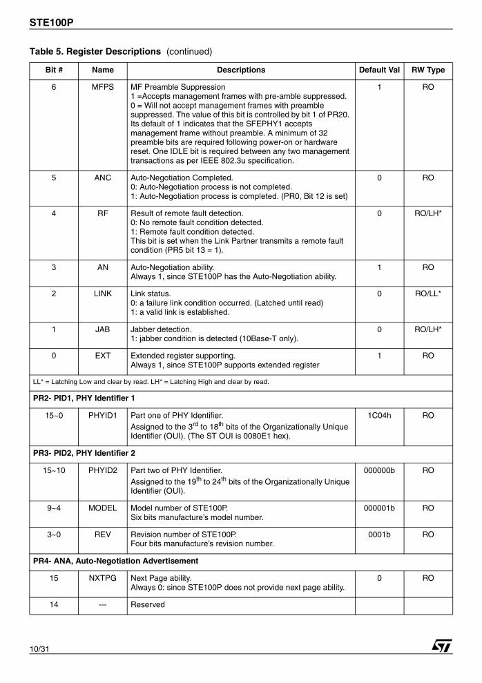
6 MFPS MF Preamble Suppression 1 =Accepts management frames with pre-amble suppressed. 0 = Will not accept management frames with preamble suppressed. The value of this bit is controlled by bit 1 of PR20. Its default of 1 indicates that the SFEPHY1 accepts management frame without preamble. A minimum of 32 preamble bits are required following power-on or hardware reset. One IDLE bit is required between any two management transactions as per IEEE 802.3u specification.
1 RO
5 ANC Auto-Negotiation Completed. 0: Auto-Negotiation process is not completed.1: Auto-Negotiation process is completed. (PR0, Bit 12 is set)
0 RO
4 RF Result of remote fault detection. 0: No remote fault condition detected.1: Remote fault condition detected. This bit is set when the Link Partner transmits a remote fault condition (PR5 bit 13 = 1).
0 RO/LH*
3 AN Auto-Negotiation ability. Always 1, since STE100P has the Auto-Negotiation ability.
1 RO
2 LINK Link status. 0: a failure link condition occurred. (Latched until read)1: a valid link is established.
LL* = Latching Low and clear by read. LH* = Latching High and clear by read.
PR2- PID1, PHY Identifier 1
15~0 PHYID1 Part one of PHY Identifier. Assigned to the 3rd to 18th bits of the Organizationally Unique Identifier (OUI). (The ST OUI is 0080E1 hex).
1C04h RO
PR3- PID2, PHY Identifier 2
15~10 PHYID2 Part two of PHY Identifier. Assigned to the 19th to 24th bits of the Organizationally Unique Identifier (OUI).
000000b RO
9~4 MODEL Model number of STE100P. Six bits manufacture’s model number.
000001b RO
3~0 REV Revision number of STE100P. Four bits manufacture’s revision number.
0001b RO
PR4- ANA, Auto-Negotiation Advertisement
15 NXTPG Next Page ability. Always 0: since STE100P does not provide next page ability.
0 RO
14 --- Reserved
Table 5. Register Descriptions (continued)
Bit # Name Descriptions Default Val RW Type
11/31
STE100P
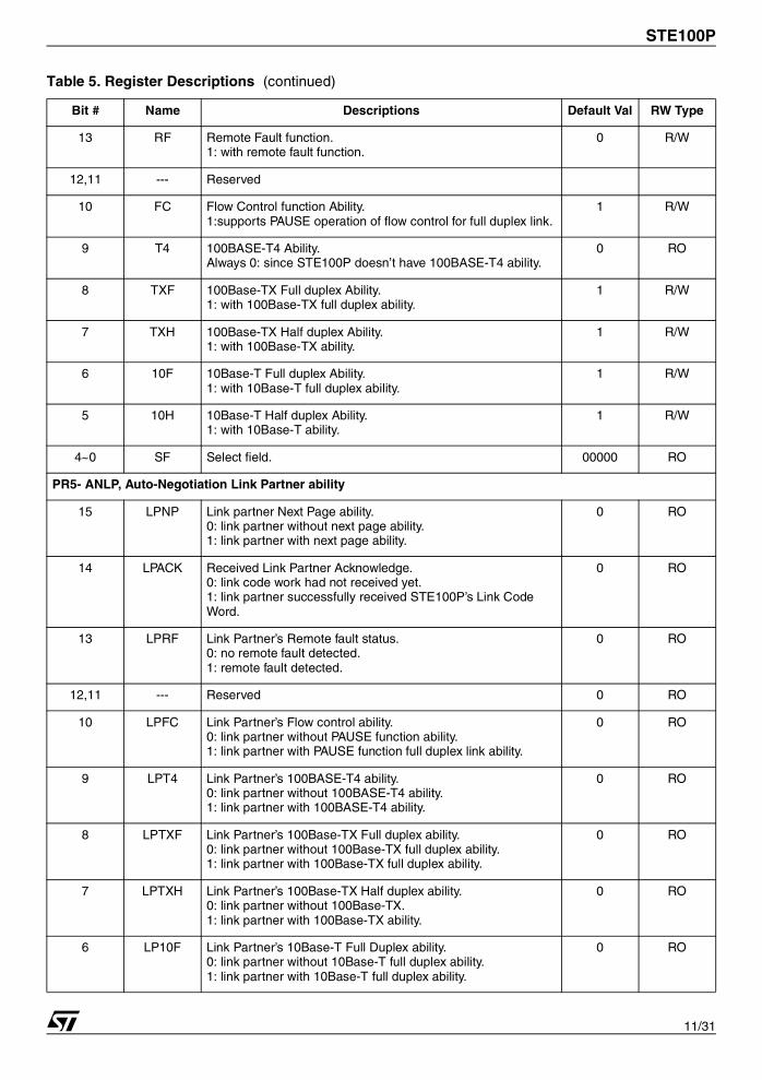
13 RF Remote Fault function. 1: with remote fault function.
0 R/W
12,11 --- Reserved
10 FC Flow Control function Ability. 1:supports PAUSE operation of flow control for full duplex link.
1 R/W
9 T4 100BASE-T4 Ability. Always 0: since STE100P doesn’t have 100BASE-T4 ability.
0 RO
8 TXF 100Base-TX Full duplex Ability. 1: with 100Base-TX full duplex ability.
1 R/W
7 TXH 100Base-TX Half duplex Ability. 1: with 100Base-TX ability.
1 R/W
6 10F 10Base-T Full duplex Ability. 1: with 10Base-T full duplex ability.
1 R/W
5 10H 10Base-T Half duplex Ability. 1: with 10Base-T ability.
1 R/W
4~0 SF Select field. 00000 RO
PR5- ANLP, Auto-Negotiation Link Partner ability
15 LPNP Link partner Next Page ability. 0: link partner without next page ability.1: link partner with next page ability.
0 RO
14 LPACK Received Link Partner Acknowledge. 0: link code work had not received yet.1: link partner successfully received STE100P’s Link Code Word.
0 RO
13 LPRF Link Partner’s Remote fault status. 0: no remote fault detected.1: remote fault detected.
0 RO
12,11 --- Reserved 0 RO
10 LPFC Link Partner’s Flow control ability. 0: link partner without PAUSE function ability.1: link partner with PAUSE function full duplex link ability.
0 RO
9 LPT4 Link Partner’s 100BASE-T4 ability. 0: link partner without 100BASE-T4 ability.1: link partner with 100BASE-T4 ability.
0 RO
8 LPTXF Link Partner’s 100Base-TX Full duplex ability. 0: link partner without 100Base-TX full duplex ability.1: link partner with 100Base-TX full duplex ability.
0 RO
7 LPTXH Link Partner’s 100Base-TX Half duplex ability. 0: link partner without 100Base-TX.1: link partner with 100Base-TX ability.
0 RO
6 LP10F Link Partner’s 10Base-T Full Duplex ability.0: link partner without 10Base-T full duplex ability. 1: link partner with 10Base-T full duplex ability.
0 RO
Table 5. Register Descriptions (continued)
Bit # Name Descriptions Default Val RW Type
STE100P
12/31
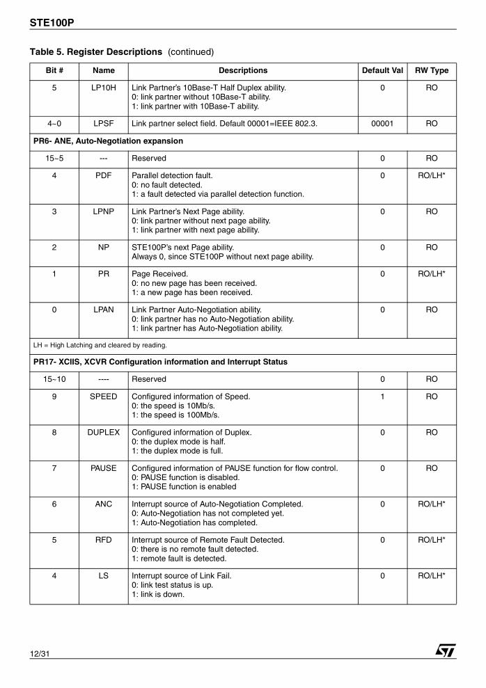
5 LP10H Link Partner’s 10Base-T Half Duplex ability. 0: link partner without 10Base-T ability.1: link partner with 10Base-T ability.
4 PDF Parallel detection fault. 0: no fault detected. 1: a fault detected via parallel detection function.
0 RO/LH*
3 LPNP Link Partner’s Next Page ability.0: link partner without next page ability. 1: link partner with next page ability.
0 RO
2 NP STE100P’s next Page ability. Always 0, since STE100P without next page ability.
0 RO
1 PR Page Received. 0: no new page has been received.1: a new page has been received.
0 RO/LH*
0 LPAN Link Partner Auto-Negotiation ability. 0: link partner has no Auto-Negotiation ability.1: link partner has Auto-Negotiation ability.
0 RO
LH = High Latching and cleared by reading.
PR17- XCIIS, XCVR Configuration information and Interrupt Status
15~10 ---- Reserved 0 RO
9 SPEED Configured information of Speed. 0: the speed is 10Mb/s. 1: the speed is 100Mb/s.
1 RO
8 DUPLEX Configured information of Duplex. 0: the duplex mode is half.1: the duplex mode is full.
0 RO
7 PAUSE Configured information of PAUSE function for flow control. 0: PAUSE function is disabled.1: PAUSE function is enabled
0 RO
6 ANC Interrupt source of Auto-Negotiation Completed. 0: Auto-Negotiation has not completed yet.1: Auto-Negotiation has completed.
0 RO/LH*
5 RFD Interrupt source of Remote Fault Detected.0: there is no remote fault detected. 1: remote fault is detected.
0 RO/LH*
4 LS Interrupt source of Link Fail.0: link test status is up. 1: link is down.
0 RO/LH*
Table 5. Register Descriptions (continued)
Bit # Name Descriptions Default Val RW Type
13/31
STE100P
3 ANAR Interrupt source of Auto-Negotiation Acknowledge Received.0: there is no link code word received.1: link code word is receive from link partner.
0 RO/LH*
2 PDF Interrupt source of Parallel Detection Fault. 0: there is no parallel detection fault.1: parallel detection is fault.
0 RO/LH*
1 ANPR Interrupt source of Auto-Negotiation Page Received.0: there is no Auto-Negotiation page received.1: auto-negotiation page is received.
0 RO/LH*
0 REF Interrupt source of Receive Error full. 0: the receive error number is less than 64.1: 64 error packets are received.
1 ANPE Auto-Negotiation Page Received interrupt Enable. 0: disable Auto-Negotiation page received interrupt.1: enable Auto-Negotiation page received interrupt.
0 R/W
0 REFE RX_ERR full interrupt Enable. 0: disable rx_err full interrupt.1: enable more than 64 time rx_err interrupt,
0 R/W
PR19- 100CTR, 100Base-TX Control Register
15,14 --- reserved
13 DISRER Disable the RX_ERR counter.0: the receive error counter - RX_ERR is enabled. 1: the receive error counter - RX_ERR is disabled.
0 R/W
12 ANC Auto-Negotiation completed. This bit is the same as PR1:5. 0: the Auto-Negotiation process has not completed yet. 1: the Auto-Negotiation process has completed.
8 ENDCR Enable DC restoration. 0: disable DC restoration.1: enable DC restoration.
1 R/W
7 ENRZI Enable the conversions between NRZ and NRZI. 0: disable the data conversion between NRZ and NRZI.1: enable the data conversion of NRZI to NRZ in receiving and NRZ to NRZI in transmitting.
1 R/W
6 EN4B5B Enable 4B/5B encoder and decoder0: the 4B/5B encoder and decoder are bypassed1: the 4B/5B encoder and decoder are enabled..
1 R/W
5 ISOTX Transmit Isolation. When 1, isolate from MII and tx+/-. The bit will be set to one if the PHY address is set to 00000 at power-up/reset This bit must be 0 for normal operation
0 R/W
4~2 CMODE Reporting of current operation mode of transceiver. 000: in auto-negotiation 001: 10Base-T half duplex 010: 100Base-TX half duplex 011: reserved 100: reserved 101: 10Base-T full duplex 110: 100Base-TX full duplex 111: isolation, auto-negotiation disable
000 RO
1 DISMLT Disable MLT3. 0: the MLT3 encoder and decoder are enabled.1: the MLT3 encoder and decoder are bypassed.
0 R/W
0 DISCRM Disable Scramble. 0: the scrambler and de-scrambler is enabled.1: the scrambler and de-scrambler are disabled.
0 R/W
PR20- XMC, XCVR Mode control
15~12 --- Reserved 0 RO
11 LD Long Distance mode of 10Base-T. 0: normal squelch level. 1: reduces 10Base-T squelch level for extended cable length.As the length of the cable increases, so does the current.
0 R/W
10~8 --- Reserved 0 RO
Table 5. Register Descriptions (continued)
Bit # Name Descriptions Default Val RW Type
15/31
STE100P
7 DEVICE OPERATION The STE100P integrates the IEEE802.3u compliant functions of PCS (Physical Coding Sub-layer), PMA(Physical Medium Attachment), and PMD(Physical Medium Dependent) for 100Base-TX, and theIEEE802.3 compliant functions of Manchester encoding/decoding and transceiver for 10Base-T. All thefunctions and operation schemes are described in the following sections.
7.1 100Base-TX Transmit OperationRegarding the 100Base-TX transmission, the device provides the transmission functions of PCS, PMA,and PMD for encoding of MII data nibbles to five-bit code-groups (4B/5B), scrambling, serialization ofscrambled code-groups, converting the serial NRZ code into NRZI code, converting the NRZI code intoMLT3 code, and then driving the MLT3 code into the category 5 Unshielded Twisted Pair cable throughan isolation transformer with the turns ratio of 1:1.
Data code-groups Encoder: In normal MII mode application, the device receives nibble type 4B data viathe TxD0~3 inputs of the MII. These inputs are sampled by the device on the rising edge of Tx-clk andpassed to the 4B/5B encoder to generate the 5B code-group used by 100Base-TX.
Idle code-groups: In order to establish and maintain the clock synchronization, the device needs to keeptransmitting signals to the medium. The device will generate Idle code-groups for transmission when thereis no real data want to be sent by MAC.
Start-of-Stream Delimiter-SSD (/J/K/): In a transmission stream, the first 16 nibbles are MAC preamble.In order to let partner delineate the boundary of a data transmission sequence and to authenticate carrierevents, the device will replace the first 2 nibbles of the MAC preamble with /J/K/ code-groups.
End-of-Stream Delimiter-ESD (/T/R/): In order to indicate the termination of the normal data transmis-sions, the device will insert 2 nibbles of /T/R/ code-group after the last nibble of FCS.
Scrambling: All the encoded data(including the idle, SSD, and ESD code-groups) is passed to the datascrambler to reduce the EMI and spread the power spectrum using a 10-bit scrambler seed loaded at thebeginning.
7~3 PAD4:0 PHY Address [4:0]:The values of the PAD[4:0] pins are latched to this register at power-up/reset. The first PHY address bit transmitted or received is the MSB of the address (bit 4). A station management entity connected to multiple PHY entities must know the appropriate address of each PHY. A PHY address of <00000> that is latched in to the part at power-up/reset will cause the Isolate bit of the PR0 (bit 10, register address 00h) to be set. After power up/reset the only way to enable or disable isolate mode is to set or clear the Isolate bit (bit 10) PR0. After power up/reset writing <00000> to bits [4:0] of this register will not cause the part to enter isolate mode.
[00001] Strap,R/W
2 --- reserved 0 RO
1 MFPSE MF Preamble Suppression Enable1 = Accept management frames with pre-amble suppressed. 0 = Do not accept management frames with preamble suppressed.This bit also controls the value of bit 6 in PR1 (MFPS).
1 R/W
0 --- reserved 0 RO
Table 5. Register Descriptions (continued)
Bit # Name Descriptions Default Val RW Type
STE100P
16/31
Data conversion of Parallel to Serial, NRZ to NRZI, NRZI to MLT3: After scrambled, the transmissiondata with 5B type in 25MHz will be converted to serial bit stream in 125MHz by the parallel to serial func-tion. After serialized, the transmission serial bit stream will be further converted from NRZ to NRZI format.This NRZI conversion function can be bypassed, if the bit 7 of PR19 register is cleared as 0. After NRZIconverted, the NRZI bit stream is passed through MLT3 encoder to generate the TP-PMD specified MLT3code. With this MLT3 code, it lowers the frequency and reduces the energy of the transmission signal inthe UTP cable and also makes the system easily to meet the FCC specification of EMI.
Wave-Shaper and Media Signal Driver: In order to reduce the energy of the harmonic frequency of trans-mission signals, the device provides the wave-shaper prior to the line driver to smooth but keep symmetricthe rising/falling edge of transmission signals. The wave-shaped signals include the 100Base-TX and10Base-T both are passed to the same media signal driver. This design can simplify the external magneticconnection with single one.
7.2 100Base-TX Receive OperationRegarding the 100Base-TX receiving operation, the device provides the receiving functions of PMD, PMA,and PCS for receiving incoming data signals through category 5 UTP cable and an isolation transformerwith turns ratio of 1: 1. It includes the adaptive equalizer and baseline wander, data conversions of MLT3to NRZI, NRZI to NRZ and serial to parallel, the PLL for clock and data recovery, the de-scrambler, andthe decoder of 5B/4B.
Adaptive Equalizer and Baseline Wander: Since the high speed signals over the unshielded (or shield-ed) twisted Pair cable will induce the amplitude attenuation and phase shifting. Furthermore, these effectsare depends on the signal frequency, cable type, cable length and the connectors of the cabling. So a re-liable adaptive equalizer and baseline wander to compensate all the amplitude attenuation and phase shift-ing are necessary. In the transceiver, it provides the robust circuits to perform these functions.
MLT3 to NRZI Decoder and PLL for Data Recovery: After receiving the proper MLT3 signals, the deviceconverts the MLT3 to NRZI code for further processing. After adaptive equalizer, baseline wander, andMLT3 to NRZI decoder, the compensated signals with NRZI type in 125MHz are passed to the Phase LockLoop circuits to extract out the original data and synchronous clock.
Data Conversions of NRZI to NRZ and Serial to Parallel: After data is recovered, the signals will bepassed to the NRZI to NRZ converter to generate the 125 MHz serial bit stream. This serial bit stream willbe packed to parallel 5B type for further processing. The NRZI to NRZ conversion can be bypassed, if thebit 7 of PR19 register is cleared as 0.
De-scrambling and Decoding of 5B/4B: The parallel 5B type data is passed to de-scrambler and 5B/4Bdecoder to return their original MII nibble type data.
Carrier sensing: Carrier Sense(CRS) signal is asserted when the STE100P detects any 2 non-contiguouszeros within any 10 bit boundary of the receiving bit stream. CRS is de-asserted when ESD code-group orIdle code-group is detected. In half duplex mode, CRS is asserted during packet transmission or receive.But in full duplex mode, CRS is asserted only during packet reception.
7.3 10Base-T Transmit OperationThis includes the parallel to serial converter, Manchester Encoder, Link test function, Jabber function andthe transmit wave-shaper and line driver described in the section of “Wave-Shaper and Media Signal Driv-er” of “100BASE-T Transmission Operation”. It also provides Collision detection and SQE test for half du-plex application.
7.4 10Base-T Receive Operation This includes the carrier sense function, receiving filter, PLL for clock and data recovering, Manchesterdecoder, and serial to parallel converter.
17/31
STE100P
7.5 Loop-back Operation The STE100P provides internal loop-back option for both the 100Base-TX and 10Base-T operations. Set-ting bit 14 of PR0 register to 1 can enable the loop-back option. In this loop-back operation, the txp/txnand rxp/rxn lines are isolated from the media. The STE100P also provides remote loop-back operation for100Base-TX operation. Setting bit 9 of PR19 register to 1 enables the remote loop-back operation.
In the 100Base-TX internal loop-back operation, the data comes from the transmit output of NRZ to NRZIconverter then loop-back to the receive path into the input of NRZI to NRZ converter.
In the 100Base-TX remote loop-back operation, the data is received from rxp/rxn pins through receivepath to the output of data and clock recover and then loop-back to the input of NRZI to MLT3 converter oftransmit path then transmit out to the medium via the transmit line drivers.
In the 10Base-T loop-back operation, the data is through transmit path and loop-back from the output ofthe Manchester encoder into the input of Phase Lock Loop circuit of receive path.
7.6 Full Duplex and Half Duplex Operation The STE100P can operate for either full duplex or half duplex network application. In full duplex, bothtransmit and receive can be operated simultaneously. Under full duplex mode, collision(COL) signal is ig-nored and carrier sense(CRS) signal is asserted only when the STE100P is receiving.
In half duplex mode, either transmit or receive can be operated at one time. Under half duplex mode, col-lision signal is asserted when transmit and receive signals collided and carrier sense asserted duringtransmission and reception.
7.7 Auto-Negotiation OperationThe Auto-Negotiation function is designed to provide the means to exchange information between theSTE100P and the network partner to automatically configure both to take maximum advantage of theirabilities, and both are setup accordingly. The Auto-Negotiation function can be controlled through ANE,bit 12 of the PR0 register, or the MF0 pin 5.
Auto-Negotiation exchanges information with the network partner using the Fast Link Pulses(FLPs) - aburst of link pulses. There are 16 bits of signaling information contained in the burst pulses to advertise allremote partner’s capabilities which are determined by the register of PR4. According to this informationthey find out their highest common capability by following the priority sequence as below:
1. 100Base-TX full duplex
2. 100Base-TX half duplex
3. 10Base-T full duplex
4. 10Base-T half duplex During power-up or reset, if Auto-Negotiation is found enabled then FLPs will be transmitted and the Auto-Negotiation function will proceed. Otherwise, the Auto-Negotiation will not occur until the bit 12 of PR0 reg-ister is set to 1. When Auto-Negotiation is disabled, then the Network Speed and Duplex Mode are select-ed by programming PR0 register.
7.8 Power Down OperationTo reduce the power consumption, the STE100P is designed with a power down feature, which can savethe power consumption significantly. Since the power supply of the 100Base-TX and 10Base-T circuitsare separated, the STE100P can turn off the circuit of either the 100Base-TX or 10Base-T when the otherone of them is operating. There is also a Power Down mode which can be selected by PDEN in registerPR0 bit 11. During the Power Down mode, TXP/TXN outputs and all LED outputs are 3-stated, and theMII interface is isolated. During Power Down mode the MII management interface is still available for read-ing and writing device registers. Power Down mode can be exited by clearing bit 11 of register PR0 or bya hardware or software reset (setting PR0:15=1).
STE100P
18/31
7.9 LED Display OperationThe STE100P provides 5 LED pins, the detail descriptions about the operation are described in the PINDescription section, and as follows.
Speed LED: 100Mbps(on) or 10Mbps(off)
Receive LED: Blinks at 10Hz when receiving, but not colliding
Transmit LED: Blinks at 10Hz when transmitting, but not colliding
Link LED: On when 100M or 10M link ok
Collision LED: Blinks at 20Hz to indicate a collision
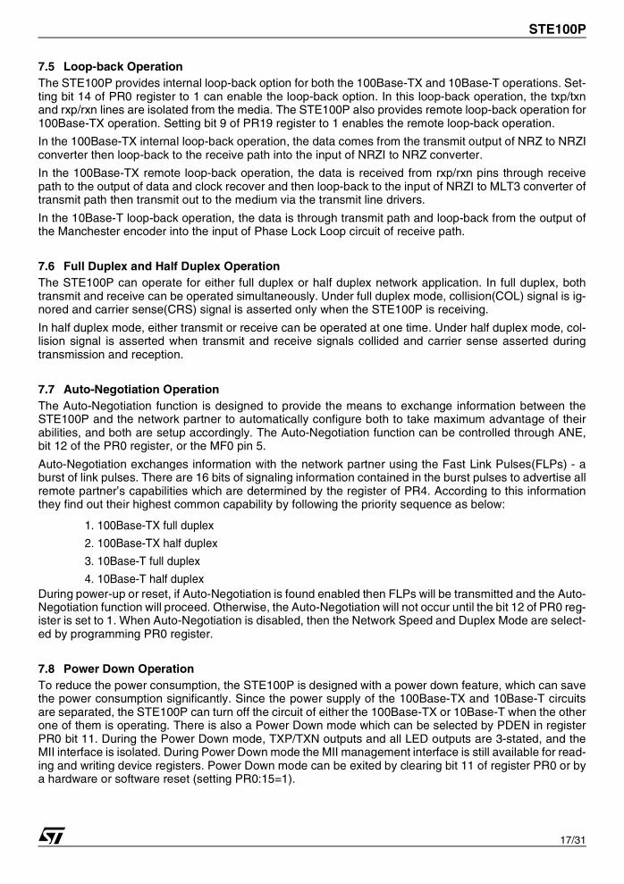
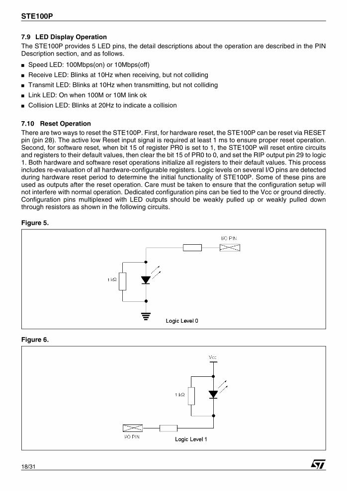
7.10 Reset OperationThere are two ways to reset the STE100P. First, for hardware reset, the STE100P can be reset via RESETpin (pin 28). The active low Reset input signal is required at least 1 ms to ensure proper reset operation.Second, for software reset, when bit 15 of register PR0 is set to 1, the STE100P will reset entire circuitsand registers to their default values, then clear the bit 15 of PR0 to 0, and set the RIP output pin 29 to logic1. Both hardware and software reset operations initialize all registers to their default values. This processincludes re-evaluation of all hardware-configurable registers. Logic levels on several I/O pins are detectedduring hardware reset period to determine the initial functionality of STE100P. Some of these pins areused as outputs after the reset operation. Care must be taken to ensure that the configuration setup willnot interfere with normal operation. Dedicated configuration pins can be tied to the Vcc or ground directly.Configuration pins multiplexed with LED outputs should be weakly pulled up or weakly pulled downthrough resistors as shown in the following circuits.
Figure 5.
Figure 6.
19/31
STE100P
Note:
The above LED connections are recommended for setting a Logic Level 1 or Logic Level 0 on theSTE100P LED/PHY Address pins, for determining PHY address.
7.11 Preamble SuppressionPreamble suppression mode in the STEPHY1 is indicated by a one in bit six of the PR1 Register. If it isdetermined that all PHY devices in the system support preamble suppression, then a preamble is not nec-essary for each management transaction. The first transaction following power-up/hardware reset re-quires 32 bits of preamble. The full 32 bit preamble is not required for each additional transaction. TheSTEPHY1 will respond to management accesses without preamble, but a minimum of one idle bit betweenmanagement transactions is required as specified in IEEE 802.3u.
7.12 Remote FaultThe remote fault function indicates to a link partner that a fault condition has occurred by using the RemoteFault bit, which is encoded in bit 13 of the Link Code Word. A local device indicates to its link partner thatit has found a fault by setting the Remote Fault bit in the Auto-Negotiation register to logic one and rene-gotiating with the link partner. The Remote Fault bit remains at logic one until successful negotiation withthe Link Code Word occurs. The bit will then return to 0. When the message is sent that the Remote Faultbit is set to logic one, the device will set the Remote Fault bit in the MII to logic one if the managementfunction is present.
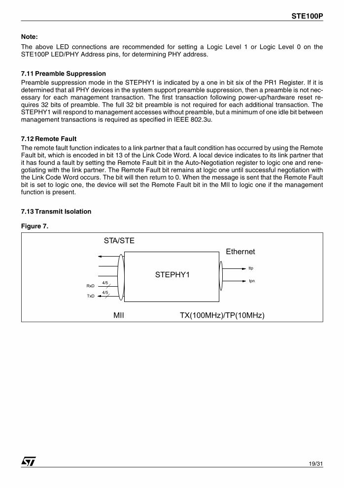
7.13 Transmit Isolation
Figure 7.
STA/STE
TxD
RxD
4/5
4/5
STEPHY1ttp
MII
tpn
TX(100MHz)/TP(10MHz)
Ethernet
STE100P
20/31
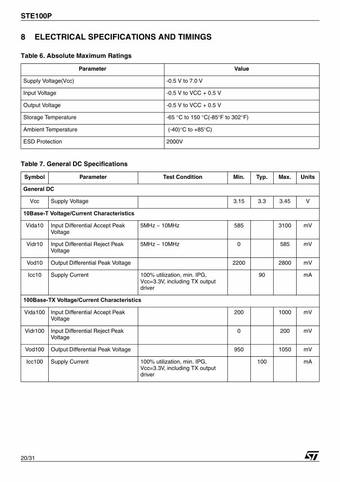
8 ELECTRICAL SPECIFICATIONS AND TIMINGS
Table 6. Absolute Maximum Ratings
Parameter Value
Supply Voltage(Vcc) -0.5 V to 7.0 V
Input Voltage -0.5 V to VCC + 0.5 V
Output Voltage -0.5 V to VCC + 0.5 V
Storage Temperature -65 °C to 150 °C(-85°F to 302°F)
Ambient Temperature (-40)°C to +85°C)
ESD Protection 2000V
Table 7. General DC Specifications
Symbol Parameter Test Condition Min. Typ. Max. Units
General DC
Vcc Supply Voltage 3.15 3.3 3.45 V
10Base-T Voltage/Current Characteristics
Vida10 Input Differential Accept Peak Voltage
5MHz ~ 10MHz 585 3100 mV
Vidr10 Input Differential Reject Peak Voltage
5MHz ~ 10MHz 0 585 mV
Vod10 Output Differential Peak Voltage 2200 2800 mV
Icc10 Supply Current 100% utilization, min. IPG, Vcc=3.3V, including TX outputdriver
90 mA
100Base-TX Voltage/Current Characteristics
Vida100 Input Differential Accept Peak Voltage
200 1000 mV
Vidr100 Input Differential Reject Peak Voltage
0 200 mV
Vod100 Output Differential Peak Voltage 950 1050 mV
Icc100 Supply Current 100% utilization, min. IPG, Vcc=3.3V, including TX outputdriver
100 mA
21/31
STE100P
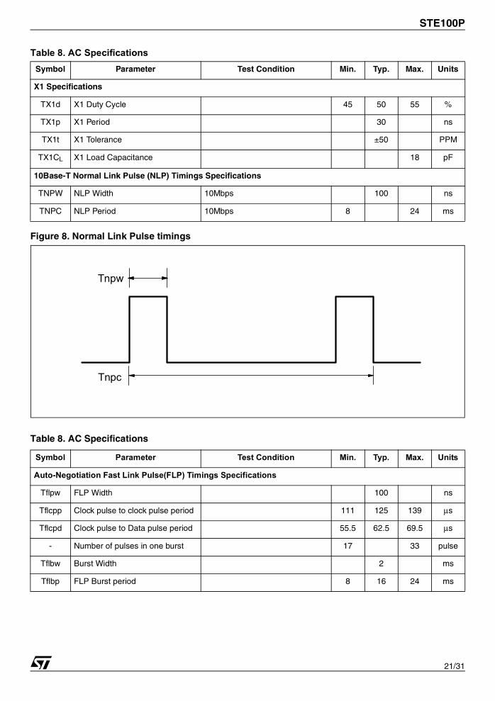
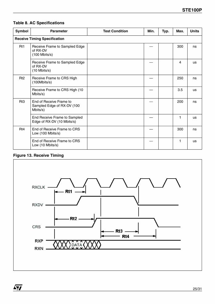
Table 8. AC Specifications
Figure 8. Normal Link Pulse timings
Symbol Parameter Test Condition Min. Typ. Max. Units
X1 Specifications
TX1d X1 Duty Cycle 45 50 55 %
TX1p X1 Period 30 ns
TX1t X1 Tolerance ±50 PPM
TX1CL X1 Load Capacitance 18 pF
10Base-T Normal Link Pulse (NLP) Timings Specifications
TNPW NLP Width 10Mbps 100 ns
TNPC NLP Period 10Mbps 8 24 ms
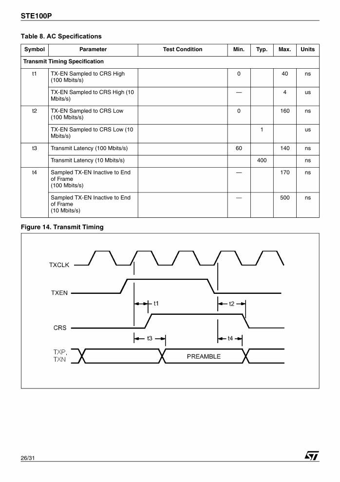
Table 8. AC Specifications
Symbol Parameter Test Condition Min. Typ. Max. Units
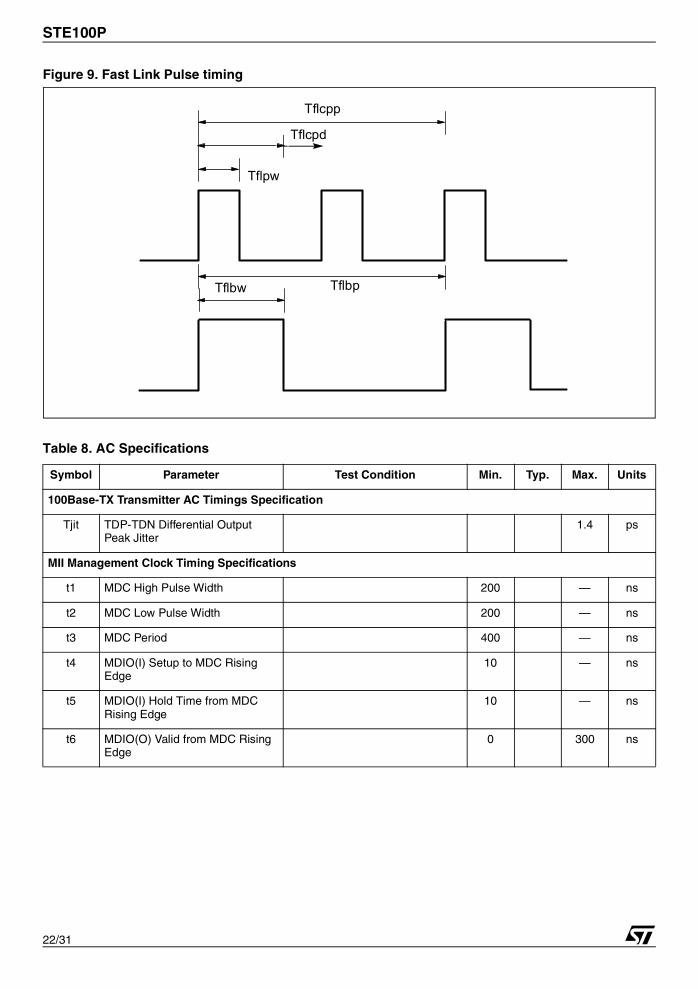
Auto-Negotiation Fast Link Pulse(FLP) Timings Specifications
Tflpw FLP Width 100 ns
Tflcpp Clock pulse to clock pulse period 111 125 139 µs
Tflcpd Clock pulse to Data pulse period 55.5 62.5 69.5 µs
- Number of pulses in one burst 17 33 pulse
Tflbw Burst Width 2 ms
Tflbp FLP Burst period 8 16 24 ms
Tnpw
Tnpc
STE100P
22/31
Figure 9. Fast Link Pulse timing
Table 8. AC Specifications
Symbol Parameter Test Condition Min. Typ. Max. Units
100Base-TX Transmitter AC Timings Specification
Tjit TDP-TDN Differential Output Peak Jitter
1.4 ps
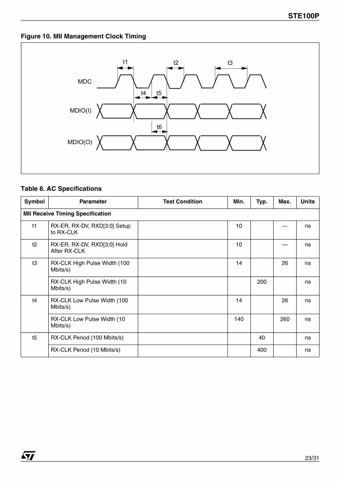
MII Management Clock Timing Specifications
t1 MDC High Pulse Width 200 — ns
t2 MDC Low Pulse Width 200 — ns
t3 MDC Period 400 — ns
t4 MDIO(I) Setup to MDC Rising Edge
10 — ns
t5 MDIO(I) Hold Time from MDC Rising Edge
10 — ns
t6 MDIO(O) Valid from MDC Rising Edge
0 300 ns
Tflpw
Tflbw Tflbp
Tflcpp
Tflcpd
23/31
STE100P
Figure 10. MII Management Clock Timing
Table 8. AC Specifications
Symbol Parameter Test Condition Min. Typ. Max. Units
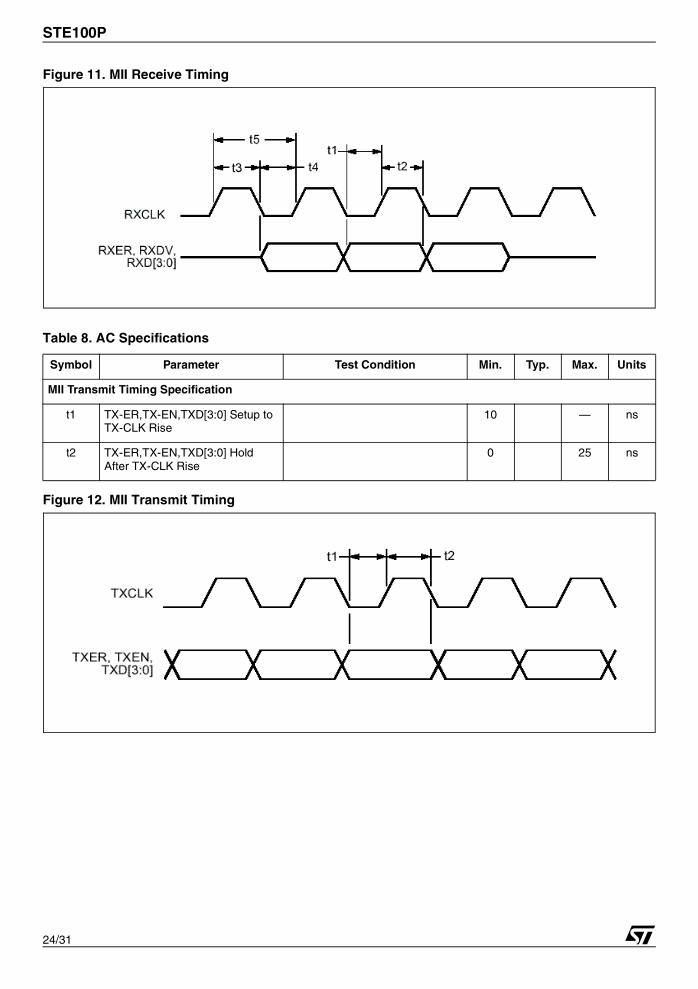
MII Receive Timing Specification
t1 RX-ER, RX-DV, RXD[3:0] Setup to RX-CLK
10 — ns
t2 RX-ER, RX-DV, RXD[3:0] Hold After RX-CLK
10 — ns
t3 RX-CLK High Pulse Width (100 Mbits/s)
14 26 ns
RX-CLK High Pulse Width (10 Mbits/s)
200 ns
t4 RX-CLK Low Pulse Width (100 Mbits/s)
14 26 ns
RX-CLK Low Pulse Width (10 Mbits/s)
140 260 ns
t5 RX-CLK Period (100 Mbits/s) 40 ns
RX-CLK Period (10 Mbits/s) 400 ns
MDC
MDIO(O)
MDIO(I)
t1 t2 t3
t4 t5
t6
STE100P
24/31
Figure 11. MII Receive Timing
Figure 12. MII Transmit Timing
Table 8. AC Specifications
Symbol Parameter Test Condition Min. Typ. Max. Units
MII Transmit Timing Specification
t1 TX-ER,TX-EN,TXD[3:0] Setup to TX-CLK Rise
10 — ns
t2 TX-ER,TX-EN,TXD[3:0] Hold After TX-CLK Rise
0 25 ns
25/31
STE100P
Table 8. AC Specifications
Figure 13. Receive Timing
Symbol Parameter Test Condition Min. Typ. Max. Units
Receive Timing Specification
Rt1 Receive Frame to Sampled Edge of RX-DV(100 Mbits/s)
— 300 ns
Receive Frame to Sampled Edge of RX-DV(10 Mbits/s)
— 4 us
Rt2 Receive Frame to CRS High (100Mbits/s)
— 250 ns
Receive Frame to CRS High (10 Mbits/s)
— 3.5 us
Rt3 End of Receive Frame to Sampled Edge of RX-DV (100 Mbits/s)
— 200 ns
End Receive Frame to Sampled Edge of RX-DV (10 Mbits/s)
— 1 us
Rt4 End of Receive Frame to CRS Low (100 Mbits/s)
— 300 ns
End of Receive Frame to CRS Low (10 Mbits/s)
— 1 us
STE100P
26/31
Table 8. AC Specifications
Figure 14. Transmit Timing
Symbol Parameter Test Condition Min. Typ. Max. Units
Transmit Timing Specification
t1 TX-EN Sampled to CRS High (100 Mbits/s)
0 40 ns
TX-EN Sampled to CRS High (10 Mbits/s)
— 4 us
t2 TX-EN Sampled to CRS Low (100 Mbits/s)
0 160 ns
TX-EN Sampled to CRS Low (10 Mbits/s)
1 us
t3 Transmit Latency (100 Mbits/s) 60 140 ns
Transmit Latency (10 Mbits/s) 400 ns
t4 Sampled TX-EN Inactive to End of Frame(100 Mbits/s)
— 170 ns
Sampled TX-EN Inactive to End of Frame (10 Mbits/s)
— 500 ns
27/31
STE100P
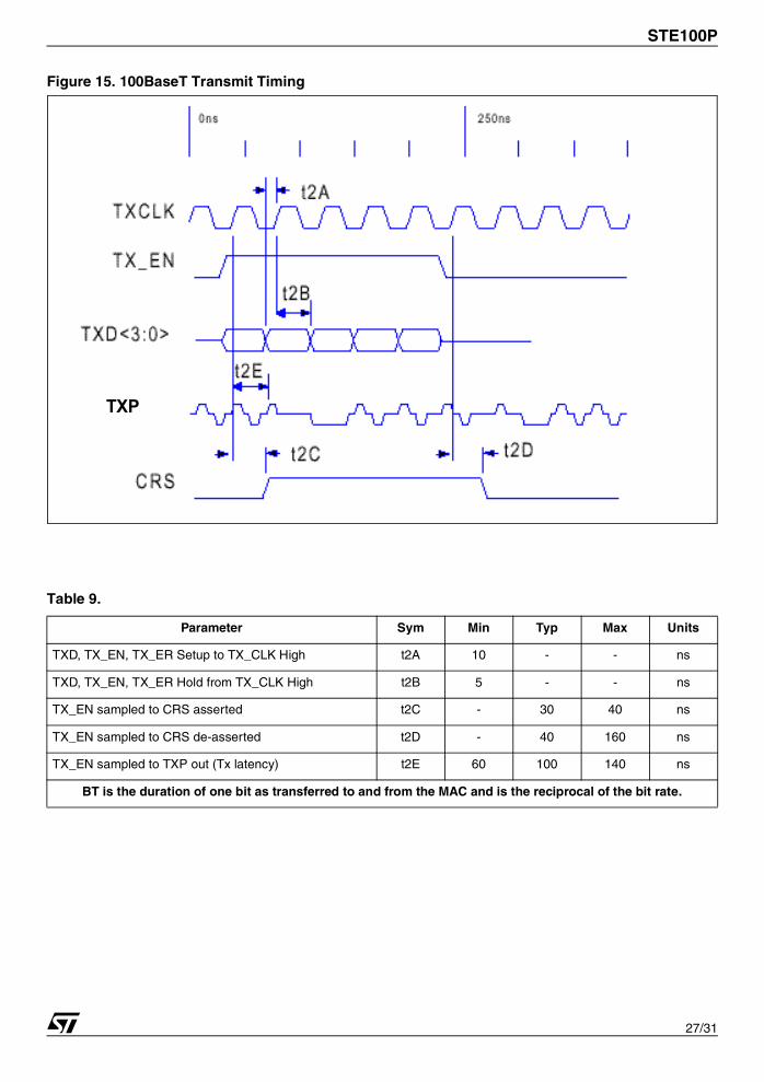
Figure 15. 100BaseT Transmit Timing
Table 9.
Parameter Sym Min Typ Max Units
TXD, TX_EN, TX_ER Setup to TX_CLK High t2A 10 - - ns
TXD, TX_EN, TX_ER Hold from TX_CLK High t2B 5 - - ns
TX_EN sampled to CRS asserted t2C - 30 40 ns
TX_EN sampled to CRS de-asserted t2D - 40 160 ns
TX_EN sampled to TXP out (Tx latency) t2E 60 100 140 ns
BT is the duration of one bit as transferred to and from the MAC and is the reciprocal of the bit rate.
TXP
STE100P
28/31
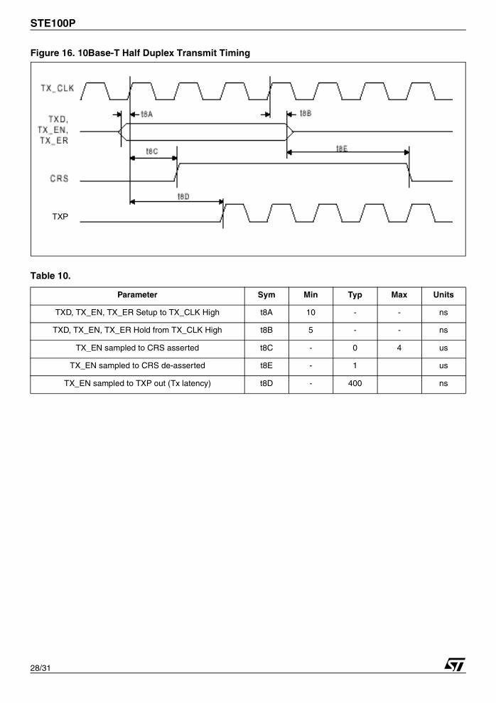
Figure 16. 10Base-T Half Duplex Transmit Timing
Table 10.
Parameter Sym Min Typ Max Units
TXD, TX_EN, TX_ER Setup to TX_CLK High t8A 10 - - ns
TXD, TX_EN, TX_ER Hold from TX_CLK High t8B 5 - - ns
TX_EN sampled to CRS asserted t8C - 0 4 us
TX_EN sampled to CRS de-asserted t8E - 1 us
TX_EN sampled to TXP out (Tx latency) t8D - 400 ns
TXP
29/31
STE100P
9 PACKAGE INFORMATIONIn order to meet environmental requirements, ST offers these devices in ECOPACK® packages. Thesepackages have a Lead-free second level interconnect. The category of second Level Interconnect ismarked on the package and on the inner box label, in compliance with JEDEC Standard JESD97.
The maximum ratings related to soldering conditions are also marked on the inner box label.ECOPACK is an ST trademark. ECOPACK specifications are available at: www.st.com.
Figure 17. TQFP64 (10x10x1.4mm) Mechanical Data & Package Dimensions
OUTLINE ANDMECHANICAL DATA
A
A2A1
B
C16
17
32
334849
64
E3
D3
E1 E
D1
D
e
1
K
B
TQFP64
L
L1
Seating Plane
0.08mm
DIM.mm inch
MIN. TYP. MAX. MIN. TYP. MAX.
A 1.60 0.063
A1 0.05 0.15 0.002 0.006
A2 1.35 1.40 1.45 0.053 0.055 0.057
B 0.17 0.22 0.27 0.0066 0.0086 0.0106
C 0.09 0.0035
D 11.80 12.00 12.20 0.464 0.472 0.480
D1 9.80 10.00 10.20 0.386 0.394 0.401
D3 7.50 0.295
e 0.50 0.0197
E 11.80 12.00 12.20 0.464 0.472 0.480
E1 9.80 10.00 10.20 0.386 0.394 0.401
E3 7.50 0.295
L 0.45 0.60 0.75 0.0177 0.0236 0.0295
L1 1.00 0.0393
K 0˚ (min.), 3.5˚ (min.), 7˚(max.)
ccc 0.080 0.0031
TQFP64 (10 x 10 x 1.4mm)
0051434 E
ccc
STE100P
30/31
Table 11. Revision History
Date Revision Description of Changes
January 2004 15 Rev. A12 June 2003 has been migrated from ST-PRESS to EDOCS.
June 2004 16 Changed the Style-sheet on the Rev. A13.
August 2004 17 Wrong package corrected.
September 2004 18 Due to Rev. 17 content was partially wrong. Now fixed.
February 2005 19 Added part number “E-STE100P” (ECOPACK).
Information furnished is believed to be accurate and reliable. However, STMicroelectronics assumes no responsibility for the consequencesof use of such information nor for any infringement of patents or other rights of third parties which may result from its use. No license is grantedby implication or otherwise under any patent or patent rights of STMicroelectronics. Specifications mentioned in this publication are subjectto change without notice. This publication supersedes and replaces all information previously supplied. STMicroelectronics products are notauthorized for use as critical components in life support devices or systems without express written approval of STMicroelectronics.
The ST logo is a registered trademark of STMicroelectronics.All other names are the property of their respective owners
STMicroelectronics group of companiesAustralia - Belgium - Brazil - Canada - China - Czech Republic - Finland - France - Germany - Hong Kong - India - Israel - Italy - Japan -
Malaysia - Malta - Morocco - Singapore - Spain - Sweden - Switzerland - United Kingdom - United States of Americawww.st.com