• Quiet-Wire® technology to reduce line emissions and enhance immunity
• Ultra-Deep Sleep standby mode
• AEC-Q100 Grade 2 Automotive Qualified
Target Applications
• Industrial Control
• Vehicle On-Board Diagnostics (OBD)
• Automotive Gateways
• Camera and Sensor Networking
• Infotainment
Key Benefits
• Quiet-Wire Programmable EMI Filter
• RMII Interface with MDC/MDIO Management Interface for Register Configuration
• On-Chip Termination Resistors for Differential Pairs
• LinkMD®+ Receive Signal Quality Indicator
• Fast Start-Up and Link
• Ultra Deep Sleep Standby Mode; CPU or Signal Detect Activated
• Loopback Modes for Diagnostics
• Programmable Interrupt Output
2016-2018 Microchip Technology Inc. DS00002197E-page 1
KSZ8061RNB/RND
TO OUR VALUED CUSTOMERS
It is our intention to provide our valued customers with the best documentation possible to ensure successful use of your Microchipproducts. To this end, we will continue to improve our publications to better suit your needs. Our publications will be refined andenhanced as new volumes and updates are introduced.
If you have any questions or comments regarding this publication, please contact the Marketing Communications Department viaE-mail at [email protected]. We welcome your feedback.
Most Current Data SheetTo obtain the most up-to-date version of this data sheet, please register at our Worldwide Web site at:
http://www.microchip.com
You can determine the version of a data sheet by examining its literature number found on the bottom outside corner of any page. The last character of the literature number is the version number, (e.g., DS30000000A is version A of document DS30000000).
ErrataAn errata sheet, describing minor operational differences from the data sheet and recommended workarounds, may exist for cur-rent devices. As device/documentation issues become known to us, we will publish an errata sheet. The errata will specify therevision of silicon and revision of document to which it applies.
To determine if an errata sheet exists for a particular device, please check with one of the following:• Microchip’s Worldwide Web site; http://www.microchip.com• Your local Microchip sales office (see last page)
When contacting a sales office, please specify which device, revision of silicon and data sheet (include -literature number) you areusing.
Customer Notification SystemRegister on our web site at www.microchip.com to receive the most current information on all of our products.
DS00002197E-page 2 2016-2018 Microchip Technology Inc.
2016-2018 Microchip Technology Inc. DS00002197E-page 3
KSZ8061RNB/RND
Table of Contents
1.0 Introduction ..................................................................................................................................................................................... 42.0 Pin Description and Configuration .................................................................................................................................................. 53.0 Functional Description .................................................................................................................................................................... 94.0 Register Map ................................................................................................................................................................................. 255.0 Operational Characteristics ........................................................................................................................................................... 386.0 Electrical Characteristics ............................................................................................................................................................... 397.0 Timing Diagrams ........................................................................................................................................................................... 428.0 Reset Circuit ................................................................................................................................................................................. 469.0 Reference Clock Connection and Selection - KSZ8061RNB ........................................................................................................ 4710.0 Reference Clock Connection - KSZ8061RND ............................................................................................................................ 4811.0 Package Outlines ........................................................................................................................................................................ 49Appendix A: Data Sheet Revision History ........................................................................................................................................... 51The Microchip Web Site ...................................................................................................................................................................... 52Customer Change Notification Service ............................................................................................................................................... 52Customer Support ............................................................................................................................................................................... 52Product Identification System ............................................................................................................................................................. 53
KSZ8061RNB/RND
DS00002197E-page 4 2016-2018 Microchip Technology Inc.
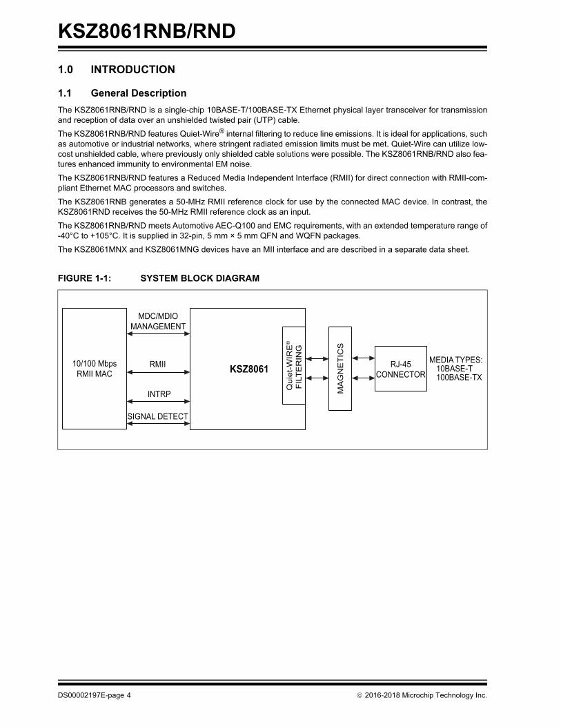
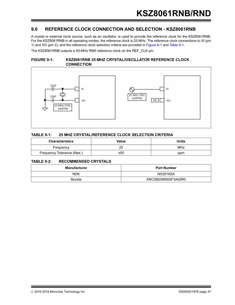
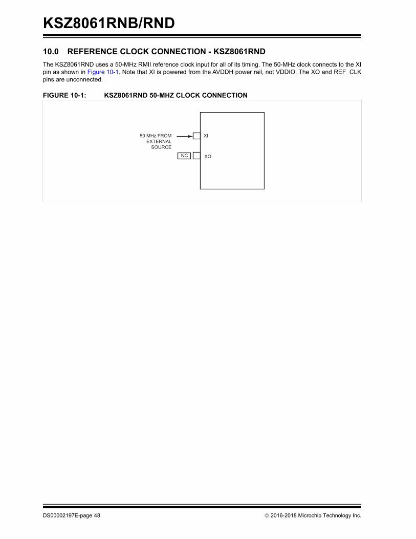
1.0 INTRODUCTION
1.1 General Description
The KSZ8061RNB/RND is a single-chip 10BASE-T/100BASE-TX Ethernet physical layer transceiver for transmissionand reception of data over an unshielded twisted pair (UTP) cable.
The KSZ8061RNB/RND features Quiet-Wire® internal filtering to reduce line emissions. It is ideal for applications, suchas automotive or industrial networks, where stringent radiated emission limits must be met. Quiet-Wire can utilize low-cost unshielded cable, where previously only shielded cable solutions were possible. The KSZ8061RNB/RND also fea-tures enhanced immunity to environmental EM noise.
The KSZ8061RNB/RND features a Reduced Media Independent Interface (RMII) for direct connection with RMII-com-pliant Ethernet MAC processors and switches.
The KSZ8061RNB generates a 50-MHz RMII reference clock for use by the connected MAC device. In contrast, theKSZ8061RND receives the 50-MHz RMII reference clock as an input.
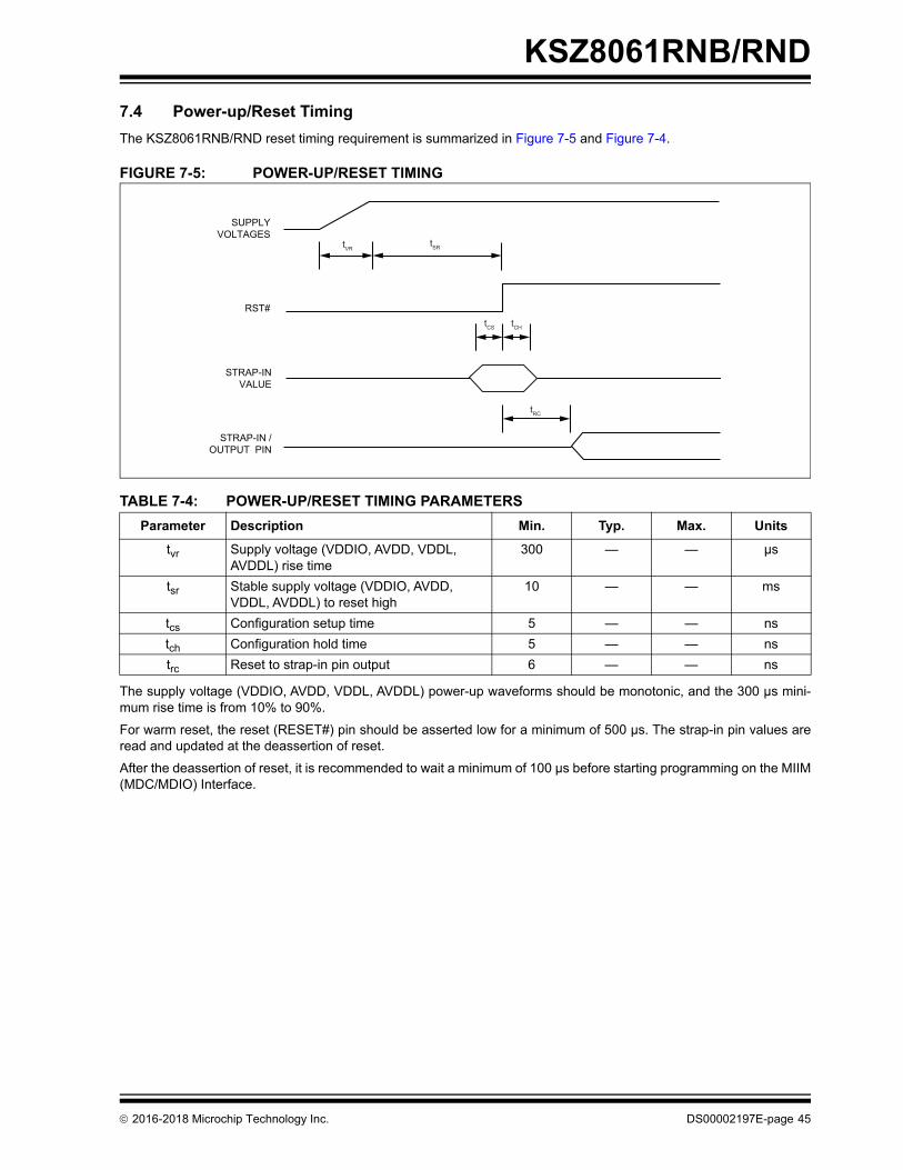
The KSZ8061RNB/RND meets Automotive AEC-Q100 and EMC requirements, with an extended temperature range of-40°C to +105°C. It is supplied in 32-pin, 5 mm × 5 mm QFN and WQFN packages.
The KSZ8061MNX and KSZ8061MNG devices have an MII interface and are described in a separate data sheet.
FIGURE 1-1: SYSTEM BLOCK DIAGRAMQ
uiet
-WIR
E®
FIL
TE
RIN
G
KSZ8061
MA
GN
ET
ICS
RJ-45CONNECTOR
MEDIA TYPES: 10BASE-T 100BASE-TX
10/100 MbpsRMII MAC
RMII
MDC/MDIOMANAGEMENT
INTRP
SIGNAL DETECT
KSZ8061RNB/RND
2.0 PIN DESCRIPTION AND CONFIGURATION
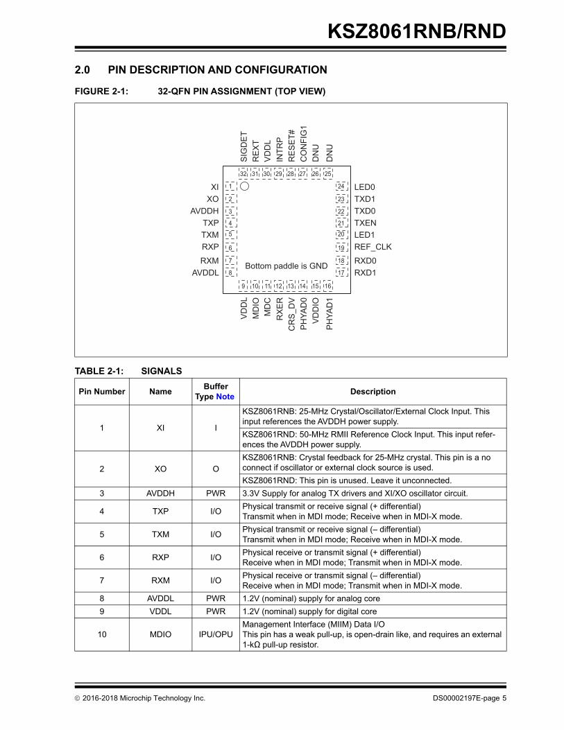
FIGURE 2-1: 32-QFN PIN ASSIGNMENT (TOP VIEW)
TABLE 2-1: SIGNALS
Pin Number NameBuffer
Type NoteDescription
1 XI I
KSZ8061RNB: 25-MHz Crystal/Oscillator/External Clock Input. This input references the AVDDH power supply.
KSZ8061RND: 50-MHz RMII Reference Clock Input. This input refer-ences the AVDDH power supply.
2 XO OKSZ8061RNB: Crystal feedback for 25-MHz crystal. This pin is a no connect if oscillator or external clock source is used.
KSZ8061RND: This pin is unused. Leave it unconnected.
3 AVDDH PWR 3.3V Supply for analog TX drivers and XI/XO oscillator circuit.
4 TXP I/OPhysical transmit or receive signal (+ differential)Transmit when in MDI mode; Receive when in MDI-X mode.
5 TXM I/OPhysical transmit or receive signal (– differential)Transmit when in MDI mode; Receive when in MDI-X mode.
6 RXP I/OPhysical receive or transmit signal (+ differential)Receive when in MDI mode; Transmit when in MDI-X mode.
7 RXM I/OPhysical receive or transmit signal (‒ differential)Receive when in MDI mode; Transmit when in MDI-X mode.
8 AVDDL PWR 1.2V (nominal) supply for analog core
9 VDDL PWR 1.2V (nominal) supply for digital core
10 MDIO IPU/OPUManagement Interface (MIIM) Data I/OThis pin has a weak pull-up, is open-drain like, and requires an external 1-kΩ pull-up resistor.
XIXO
AVDDHTXPTXMRXP
RXMAVDDL
CR
S_D
VR
XE
RM
DC
MD
IOV
DD
L
PH
YAD
0V
DD
IO
PH
YAD
1
Bottom paddle is GND
1
2
3
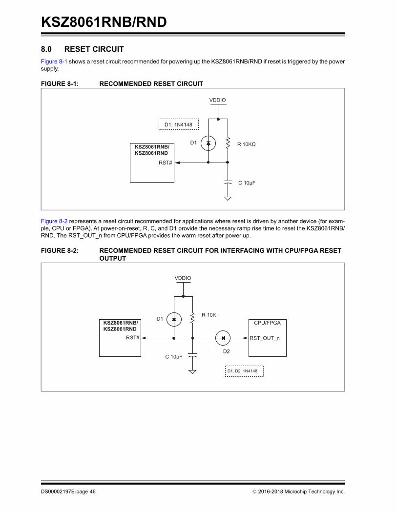
4
5
6
7
8
9 10 11 12 13 14 15 16
24
23
22
21
20
19
18
17
32 31 30 29 28 27 26 25
LED0TXD1TXD0TXENLED1REF_CLK
RXD0RXD1
RE
SE
T#IN
TRP
VD
DL
RE
XT
SIG
DE
T
CO
NFI
G1
DN
U
DN
U
2016-2018 Microchip Technology Inc. DS00002197E-page 5
KSZ8061RNB/RND
11 MDC IPUManagement Interface (MIIM) Clock InputThis clock pin is synchronous to the MDIO data pin.
12 RXER / QWF IPD/ORMII Receive Error OutputConfig Mode: The pull-up or pull-down value is latched as QWF at the deassertion of reset. See Table 2-2, "Strap-in Options" for details.
13CRS_DV / CONFIG2
IPD/ORMII Carrier Sense/Receive Data Valid OutputConfig Mode: The pull-up or pull-down value is latched as CONFIG2 at the deassertion of reset. See Table 2-2, "Strap-in Options" for details.
14 PHYAD0 IPU/ONo function during normal operationConfig Mode: The pull-up or pull-down value is latched as PHYADDR[0] at the deassertion of reset. See Table 2-2, "Strap-in Options" for details.
15 VDDIO PWR 3.3V or 2.5V supply for digital I/O
16 PHYAD1 IPD/ONo function during normal operationConfig Mode: The pull-up or pull-down value is latched as PHYADDR[1] at the deassertion of reset. See Table 2-2, "Strap-in Options" for details.
17RXD1 /
PHYAD2IPD/O
RMII Receive Data Output[1] (Note 2-2) Config Mode: The pull-up or pull-down value is latched as PHYADDR[2] at the deassertion of reset. See Table 2-2, "Strap-in Options" for details.
18RXD0 /
AUTONEGIPU/O
RMII Receive Data Output[0] (Note 2-2)Config Mode: The pull-up or pull-down value is latched as AUTONEG at the deassertion of reset. See Table 2-2, "Strap-in Options" for details.
19REF_CLK / CONFIG0
IPD/O
KSZ8061RNB: RMII 50-MHz Reference Clock Output to the MACConfig Mode: The pull-up or pull-down value is latched as CONFIG0 at the deassertion of reset. See Table 2-2, "Strap-in Options" for details.
KSZ8061RND: This pin is unused during normal operation. Leave it unconnected except as required for Config Mode.Config Mode: The pull-up or pull-down value is latched as CONFIG0 at the deassertion of reset. See Table 2-2, "Strap-in Options" for details.
20 LED1 OLED1 OutputActive low. Its function is programmable; by default it indicates link speed.
21 TXEN I PMII Transmit Enable Input
22 TXD0 I RMII Transmit Data Input[0 (Note 2-3)
23 TXD1 I RMII Transmit Data Input[1] (Note 2-3)
24 LED0 IPD/OLED0 OutputActive low. Its function is programmable; by default it indicates link/activity.
25 DNU I Do Not Use. This unused input must be pulled to a logic-low level.
26 DNU I Do Not Use. This unused input should be pulled to a logic-low level.
27 CONFIG1 IPD/ONo function during normal operationConfig Mode: The pull-up or pull-down value is latched as CONFIG1 at the deassertion of reset. See Table 2-2, "Strap-in Options" for details.
28 RESET# IPU Chip Reset (active-low)
29INTRP /
NAND_TREE#IPU/O
Programmable Interrupt Output (active-low [default] or active-high)This pin has a weak pull-up, is open-drain like, and requires an external 1.0-kΩ pull-up resistor.Config Mode: The pull-up or pull-down value is latched as NAND_Tree# at the deassertion of reset. See Table 2-2, "Strap-in Options" for details.
30 VDDL PWR 1.2V (nominal) supply for digital (and analog)
TABLE 2-1: SIGNALS (CONTINUED)
Pin Number NameBuffer
Type NoteDescription
DS00002197E-page 6 2016-2018 Microchip Technology Inc.
KSZ8061RNB/RND
Note 2-1 Pwr = Power supplyGnd = GroundI = InputO = OutputI/O = Bi-directionalIpu = Input with internal pull-up (see Electrical Characteristics for value)Ipd = Input with internal pull-down (see Electrical Characteristics for value)Ipu/O = Input with internal pull-up (see Electrical Characteristics for value) during power-up or reset;output pin otherwise.Ipd/O = Input with internal pull-down (see Electrical Characteristics for value) during power-up orreset; output pin otherwise.Ipu/Opu = Input and output with internal pull-up (see Electrical Characteristics for value)
Note 2-2 RMII Mode: The RXD[3:0] bits are synchronous with RXC. When RXDV is asserted, RXD[3:0]presents valid data to the MAC device.
Note 2-3 RMII Mode: The TXD[3:0] bits are synchronous with TXC. When TXEN is asserted, TXD[3:0] acceptsvalid data from the MAC device.
31 REXT ISet PHY transmit output current.Connect a 6.04Ω 1% resistor from this pin to ground.
32 SIGDET O Signal Detect, active-high
Bottom Paddle GND GND Ground. Bottom paddle.
TABLE 2-1: SIGNALS (CONTINUED)
Pin Number NameBuffer
Type NoteDescription
2016-2018 Microchip Technology Inc. DS00002197E-page 7
KSZ8061RNB/RND
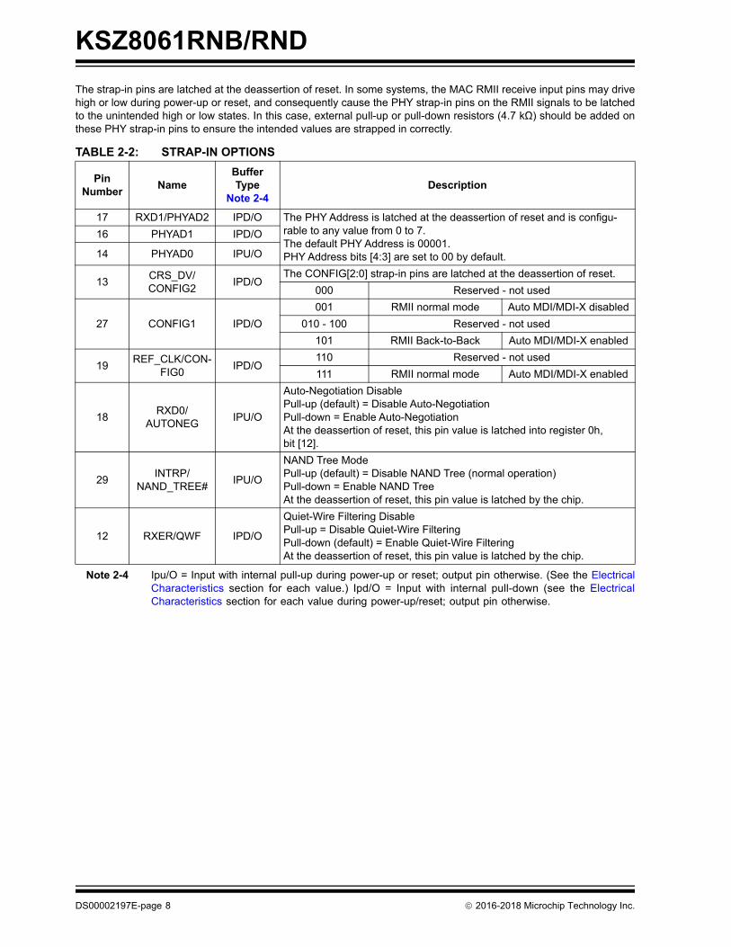
The strap-in pins are latched at the deassertion of reset. In some systems, the MAC RMII receive input pins may drivehigh or low during power-up or reset, and consequently cause the PHY strap-in pins on the RMII signals to be latchedto the unintended high or low states. In this case, external pull-up or pull-down resistors (4.7 kΩ) should be added onthese PHY strap-in pins to ensure the intended values are strapped in correctly.
Note 2-4 Ipu/O = Input with internal pull-up during power-up or reset; output pin otherwise. (See the ElectricalCharacteristics section for each value.) Ipd/O = Input with internal pull-down (see the ElectricalCharacteristics section for each value during power-up/reset; output pin otherwise.
TABLE 2-2: STRAP-IN OPTIONS
Pin Number
NameBuffer Type
Note 2-4Description
17 RXD1/PHYAD2 IPD/O The PHY Address is latched at the deassertion of reset and is configu-rable to any value from 0 to 7.The default PHY Address is 00001.PHY Address bits [4:3] are set to 00 by default.
16 PHYAD1 IPD/O
14 PHYAD0 IPU/O
13CRS_DV/CONFIG2
IPD/OThe CONFIG[2:0] strap-in pins are latched at the deassertion of reset.
000 Reserved - not used
27 CONFIG1 IPD/O
001 RMII normal mode Auto MDI/MDI-X disabled
010 - 100 Reserved - not used
101 RMII Back-to-Back Auto MDI/MDI-X enabled
19REF_CLK/CON-
FIG0IPD/O
110 Reserved - not used
111 RMII normal mode Auto MDI/MDI-X enabled
18RXD0/
AUTONEGIPU/O
Auto-Negotiation DisablePull-up (default) = Disable Auto-NegotiationPull-down = Enable Auto-NegotiationAt the deassertion of reset, this pin value is latched into register 0h, bit [12].
29INTRP/
NAND_TREE#IPU/O
NAND Tree ModePull-up (default) = Disable NAND Tree (normal operation)Pull-down = Enable NAND TreeAt the deassertion of reset, this pin value is latched by the chip.
12 RXER/QWF IPD/O
Quiet-Wire Filtering DisablePull-up = Disable Quiet-Wire FilteringPull-down (default) = Enable Quiet-Wire FilteringAt the deassertion of reset, this pin value is latched by the chip.
DS00002197E-page 8 2016-2018 Microchip Technology Inc.
KSZ8061RNB/RND
3.0 FUNCTIONAL DESCRIPTION
The KSZ8061RNB/RND is an integrated Fast Ethernet transceiver that features Quiet-Wire internal filtering to reduceline emissions. When Quiet-Wire filtering is disabled, it is fully compliant with the IEEE 802.3 specification. TheKSZ8061RNB/RND also has a high noise immunity.
On the copper media side, the KSZ8061RNB/RND supports 10BASE-T and 100BASE-TX for transmission and recep-tion of data over a standard CAT-5 or a similar unshielded twisted pair (UTP) cable, and HP Auto MDI/MDI-X for reliabledetection of and correction for straight-through and crossover cables.
On the MAC processor side, the KSZ8061RNB/RND offers the Reduced Media Independent Interface (RMII) for directconnection with RMII-compliant Ethernet MAC processors and switches.
The RMII management bus gives the MAC processor complete access to the KSZ8061RNB/RND control and statusregisters. Additionally, an interrupt pin eliminates the need for the processor to poll for PHY status change.
Auto-negotiation and Auto MDI/MDIX can be disabled at power-on to significantly reduce initial time to link up.
A signal detect pin (SIGDET) is available to indicate when the link partner is inactive. An option is available for theKSZ8061RNB/RND to automatically enter Ultra-Deep Sleep mode when SIGDET is deasserted. Ultra-Deep Sleepmode may also be entered by command of the MAC processor. Additional low power modes are available.
3.1 10BASE-T/100BASE-TX Transceiver
3.1.1 100BASE-TX TRANSMIT
The 100BASE-TX transmit function performs parallel-to-serial conversion, 4B/5B encoding, scrambling, NRZ-to-NRZIconversion, and MLT3 encoding and transmission.
The circuitry starts with a parallel-to-serial conversion, which converts the RMII data from the MAC into a 125-MHz serialbit stream. The data and control stream is then converted into 4B/5B coding and followed by a scrambler. The serializeddata is further converted from NRZ-to-NRZI format, and then transmitted in MLT3 current output. The output current isset by a precision external resistor on REXT for the 1:1 transformer ratio.
The output signal has a typical rise or fall time of 4 ns and complies with the ANSI TP-PMD standard regarding amplitudebalance, overshoot, and timing jitter. The wave-shaped 10BASE-T output is also incorporated into the 100BASE-TXtransmitter.
3.1.2 100BASE-TX RECEIVE
The 100BASE-TX receiver function performs adaptive equalization, DC restoration, MLT3-to-NRZI conversion, data andclock recovery, NRZI-to-NRZ conversion, descrambling, 4B/5B decoding, and serial-to-parallel conversion.
The receiving side starts with the equalization filter to compensate for inter-symbol interference (ISI) over the twistedpair cable. Because the amplitude loss and phase distortion is a function of the cable length, the equalizer must adjustits characteristics to optimize performance. In this design, the variable equalizer makes an initial estimation based oncomparisons of incoming signal strength against some known cable characteristics, and then tunes itself for optimiza-tion. This is an ongoing process and self-adjusts against environmental changes, such as temperature variations.
Next, the equalized signal goes through a DC restoration and data conversion block. The DC restoration circuit is usedto compensate for the effect of baseline wander and to improve the dynamic range. The differential data conversioncircuit converts the MLT3 format back to NRZI. The slicing threshold is also adaptive.
The clock recovery circuit extracts the 125-MHz clock from the edges of the NRZI signal. This recovered clock is thenused to convert the NRZI signal into the NRZ format. This signal is sent through the descrambler followed by the 4B/5Bdecoder. Finally, the NRZ serial data is converted to the RMII format and provided as the input data to the MAC.
3.1.3 SCRAMBLER/DE-SCRAMBLER (100BASE-TX ONLY)
The scrambler is used to spread the power spectrum of the transmitted signal to reduce EMI and baseline wander. Thedescrambler is needed to recover the scrambled signal.
3.1.4 10BASE-T TRANSMIT
The 10BASE-T drivers are incorporated with the 100BASE-TX drivers to allow for transmission using the same mag-netic. The drivers perform internal wave-shaping and pre-emphasis, then output 10BASE-T signals with a typical ampli-tude of 2.5V peak. The 10BASE-T signals have harmonic contents that are at least 27 dB below the fundamentalfrequency when driven by an all-ones Manchester-encoded signal.
2016-2018 Microchip Technology Inc. DS00002197E-page 9
KSZ8061RNB/RND
3.1.5 10BASE-T RECEIVE
On the receive side, input buffer and level detecting squelch circuits are employed. A differential input receiver circuitand a PLL performs the decoding function. The Manchester-encoded data stream is separated into clock signal andNRZ data. A squelch circuit rejects signals with levels less than 400 mV or with short pulse widths to prevent noise atthe RXP and RXM inputs from falsely triggering the decoder. When the input exceeds the squelch limit, the PLL locksonto the incoming signal and the KSZ8061RNB/RND decodes a data frame. The receive clock is kept active during idleperiods in between data reception.
3.1.6 PLL CLOCK SYNTHESIZER
The KSZ8061RNB/RND generates all internal clocks and all external clocks for system timing from the clock receivedat the XI pin. For the KSZ8061RNB, this is an external 25-MHz crystal, oscillator, or reference clock. For theKSZ8061RND, this is the externally supplied RMII 50-MHz reference clock.
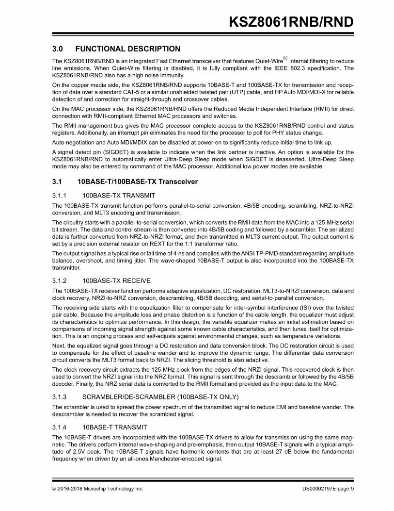
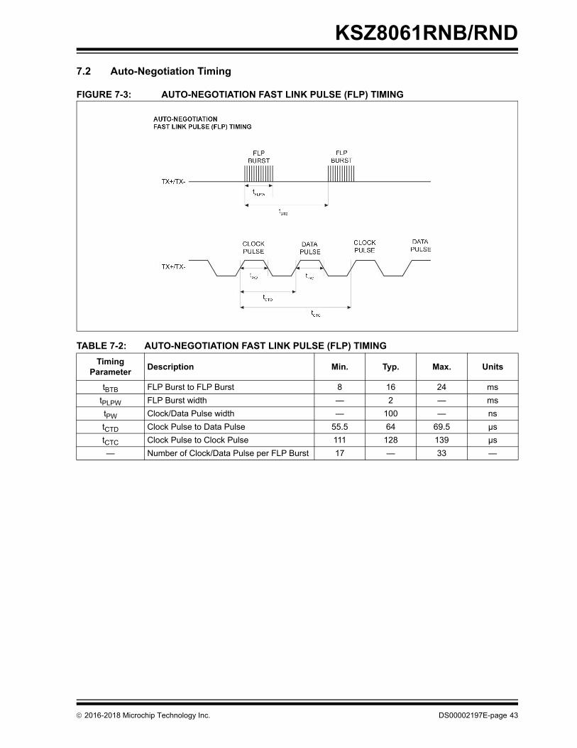
3.1.7 AUTO-NEGOTIATION
The KSZ8061RNB/RND conforms to the auto-negotiation protocol, defined in Clause 28 of the IEEE 802.3 Specifica-tion.
Auto-negotiation allows unshielded twisted pair (UTP) link partners to select the highest common mode of operation.
During auto-negotiation, link partners advertise capabilities across the UTP link to each other, and then compare theirown capabilities with those they received from their link partners. The highest speed and duplex setting that is commonto the two link partners is selected as the mode of operation.
The following list shows the speed and duplex operation mode from highest to lowest priority:
• Priority 1: 100BASE-TX, full-duplex
• Priority 2: 100BASE-TX, half-duplex
• Priority 3: 10BASE-T, full-duplex
• Priority 4: 10BASE-T, half-duplex
If the KSZ8061RNB/RND is using auto-negotiation, but its link partner is not, then the KSZ8061RNB/RND sets its oper-ating speed by observing the signal at its receiver. This is known as parallel detection, and allows the KSZ8061RNB/RND to establish a link by listening for a fixed signal protocol in the absence of auto-negotiation advertisement protocol.Duplex is set by register 0h, bit [8] because the KSZ8061RNB/RND cannot determine duplex by parallel detection.
If auto-negotiation is disabled, the speed is set by register 0h, bit [13], and the duplex is set by register 0h, bit [8]. Thedefault is 100BASE-TX, full-duplex.
Auto-negotiation is enabled or disabled by hardware pin strapping (AUTONEG) and by software (register 0h, bit [12]).By default, auto-negotiation is disabled after power-up or hardware reset, but it may be enabled by pulling the RXD0 pinlow at that time. Afterwards, auto-negotiation can be enabled or disabled by register 0h, bit [12].
When the link is 10BASE-T or the link partner is using auto-negotiation and the Ultra-Deep Sleep mode is used, thenthe Signal Detect assertion timing delay bit, register 14h bit [1], must be set.
The auto-negotiation link-up process is shown in Figure 3-1.
DS00002197E-page 10 2016-2018 Microchip Technology Inc.
KSZ8061RNB/RND
FIGURE 3-1: AUTO-NEGOTIATION FLOW CHART
3.2 Quiet-Wire® Filtering
Quiet-Wire is a feature to enhance 100BASE-TX EMC performance by reducing both conducted and radiated emissionsfrom the TXP/M signal pair. It can be used either to reduce absolute emissions or to enable replacement of shieldedcable with unshielded cable, all while maintaining interoperability with standard 100BASE-TX devices.
Quiet-Wire filtering is implemented internally, with no additional external components required. It is enabled or disabledat power-up and reset by a strapping option on the RXER pin. Once the KSZ8061 is powered up, Quiet-Wire filteringcan be disabled by writing to register 16h, bit [12]. Note that Quiet-Wire cannot be enabled via this register bit.
The default setting for Quiet-Wire reduces emissions primarily above 60 MHz, with less reduction at lower frequencies.Several dB of reduction is possible. Signal attenuation is approximately equivalent to increasing the cable length by 10to 20 meters, thus reducing cable reach by that amount. For applications needing more modest improvement in emis-sions, the level of filtering can be reduced by writing a series of registers.
3.3 Fast Link-Up
Link-up time is normally determined by the time it takes to complete auto-negotiation. Additional time may be added bythe auto MDI/MDI-X feature. The total link-up time from power-up or cable connect is typically a second or more.
Fast Link-up mode significantly reduces 100BASE-TX link-up time by disabling both auto-negotiation and auto MDI/MDI-X, and fixing the TX and RX channels. This is done via the CONFIG[2:0] and AUTONEG strapping options.Because these are strapping options, fast link-up is available immediately upon power-up. Fast Link-up is available onlyfor 100BASE-TX link speed. To force the link speed to 10BASE-TX requires a register write.
Fast Link-up mode is intended for specialized applications where both link partners are known in advance. The link mustalso be known so that the fixed transmit channel of one device connects to the fixed receive channel of the other device,and vice versa.
If a device in Fast Link-up mode is connected to a normal device (auto-negotiate and auto-MDI/MDI-X), there are noproblems linking, but the speed advantage of Fast Link-up is realized only on one end.
2016-2018 Microchip Technology Inc. DS00002197E-page 11
KSZ8061RNB/RND
3.4 Internal and External RX Termination
By default, the RX differential pair is internally terminated. This minimizes the board component count by eliminating allcomponents between the KSZ8061RNB/RND and the magnetics (transformer and common mode choke). TheKSZ8061RNB/RND has the option to turn off the internal termination, to allow the use of external termination. Externaltermination does increase the external component count, but these external components can be of tighter tolerance thanthe internal termination resistors. Enabling or disabling of the internal RX termination is controlled by register 14h, bit [2].
If external termination is used in place of the internal termination, it should consist of two 50Ω resistors in series betweenRXP and RXM, with a 0.1 μF to 1 μF capacitor from the midpoint of the two resistors to ground.
3.5 RMII Interface
The Reduced Media Independent Interface (RMII) specifies a low pin count Media Independent Interface. It provides acommon interface between RMII PHYs and MACs and has the following key characteristics:
• Pin count is 8 pins (3 pins for data transmission, 4 pins for data reception, and 1 pin for the 50-MHz reference clock).
• 10-Mbps and 100-Mbps data rates are supported at both half- and full-duplex.
• Data transmission and reception are independent and belong to separate signal groups.
• Transmit data and receive data are each 2-bit wide, a di-bit.
3.6 RMII Signal Definition
Table 3-1 describes the RMII signals. Refer to RMII Specification v1.2 for detailed information.
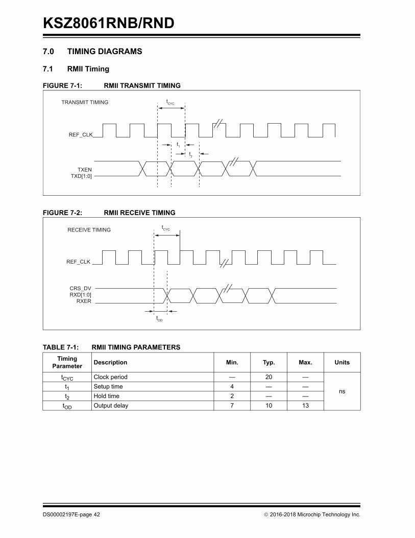
3.6.1 REFERENCE CLOCK (REF_CLK)
REF_CLK is a continuous 50-MHz clock that provides the timing reference for TXEN, TXD[1:0], CRS_DV, RXD[1:0],and RXER. The KSZ8061RNB generates and outputs the 50-MHz RMII REF_CLK to the MAC device at REF_CLK (pin19). The KSZ8061RND receives the 50-MHz RMII REF_CLK from the MAC or system board at XI (pin 1), and leavesthe REF_CLK (pin 19) as no connect.
3.6.2 TRANSMIT ENABLE (TXEN)
TXEN indicates the MAC is presenting di-bits on TXD[1:0] for transmission. It is asserted synchronously with the firstdi-bit of the preamble and remains asserted while all di-bits to be transmitted are presented on the RMII. It is negatedprior to the first REF_CLK following the final di-bit of a frame.
TXEN transitions synchronously with respect to REF_CLK.
3.6.3 TRANSMIT DATA [1:0] (TXD[1:0])
When TXEN is asserted, the PHY accepts TXD[1:0] for transmission. When TXEN is deasserted, the MAC drivesTXD[1:0] to 00 for the idle state.
TXD[1:0] transitions synchronously with respect to REF_CLK.
TABLE 3-1: RMII SIGNAL DEFINITION
RMII Signal Name
KSZ8061RNB/RND Signal and Direction
Direction(with respect to
MAC device)Description
REF_CLK KSZ8061RNB REF_CLK, Output Input Synchronous 50-MHz reference clock for receive, transmit, and control interfaceKSZ8061RND XI, Input Input or Output
TX_EN TXEN, Input Output Transmit Enable
TXD[1:0] TXD[1:0], Input Output Transmit Enable
CRS_DV CRS_DV, Output Input Carrier Sense/Receive Data Valid
RXD[1:0] RXD[1:0], Output Input Receive Data [1:0]
RX_ER RXER, Output Input Receive Error
DS00002197E-page 12 2016-2018 Microchip Technology Inc.
KSZ8061RNB/RND
3.6.4 CARRIER SENSE/RECEIVE DATA VALID (CRS_DV)
The PHY asserts CRS_DV when the receive medium is non-idle. It is asserted asynchronously when a carrier isdetected. This happens when squelch is passed in 10 Mbps mode and when two non-contiguous 0s in 10 bits aredetected in 100 Mbps mode. Loss of carrier results in the deassertion of CRS_DV.
While carrier detection criteria are met, CRS_DV remains asserted continuously from the first recovered di-bit of theframe though the final recovered di-bit. It is negated before the first REF_CLK that follows the final di-bit. The data onRXD[1:0] is considered valid after CRS_DV is asserted. However, because the assertion of CRS_DV is asynchronousrelative to REF_CLK, the data on RXD[1:0] is 00 until receive signals are properly decoded.
3.6.5 RECEIVE DATA[1:0] (RXD[1:0])
For each clock period in which CRS_DV is asserted, RXD[1:0] transfers a di-bit of recovered data from the PHY. WhenCRS_DV is deasserted, the PHY drives RXD[1:0] to 00 for the idle state.
RXD[1:0] transitions synchronously with respect to REF_CLK.
3.6.6 RECEIVE ERROR (RXER)
When CRS_DV is asserted, RXER is asserted for one or more REF_CLK periods to indicate that a symbol error (forexample, a coding error that a PHY can detect that may otherwise be undetectable by the MAC sub-layer) is detectedsomewhere in the frame that is being transferred from the PHY to the MAC.
RXER transitions synchronously with respect to REF_CLK.
3.6.7 RMII SIGNAL DIAGRAMS
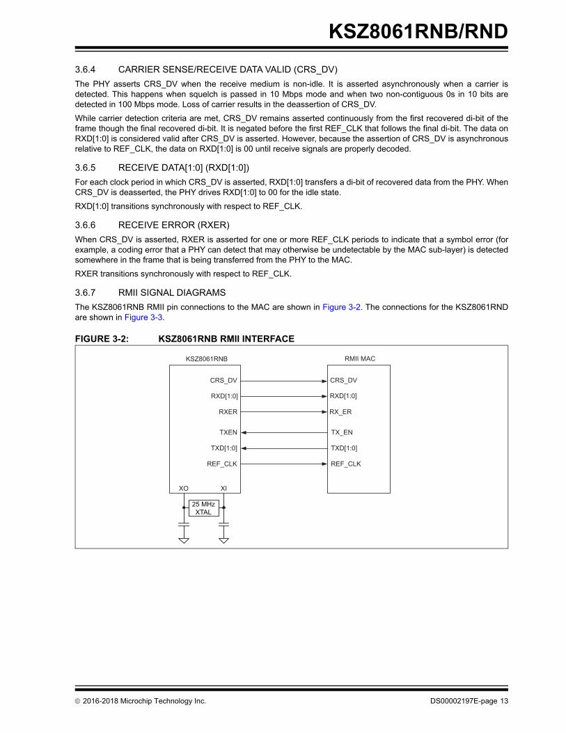
The KSZ8061RNB RMII pin connections to the MAC are shown in Figure 3-2. The connections for the KSZ8061RNDare shown in Figure 3-3.
FIGURE 3-2: KSZ8061RNB RMII INTERFACE
KSZ8061RNB
CRS_DV
RXD[1:0]
RXER
TXEN
RMII MAC
CRS_DV
RXD[1:0]
RX_ER
TX_EN
TXD[1:0] TXD[1:0]
REF_CLK REF_CLK
XO XI
25 MHzXTAL
2016-2018 Microchip Technology Inc. DS00002197E-page 13
KSZ8061RNB/RND
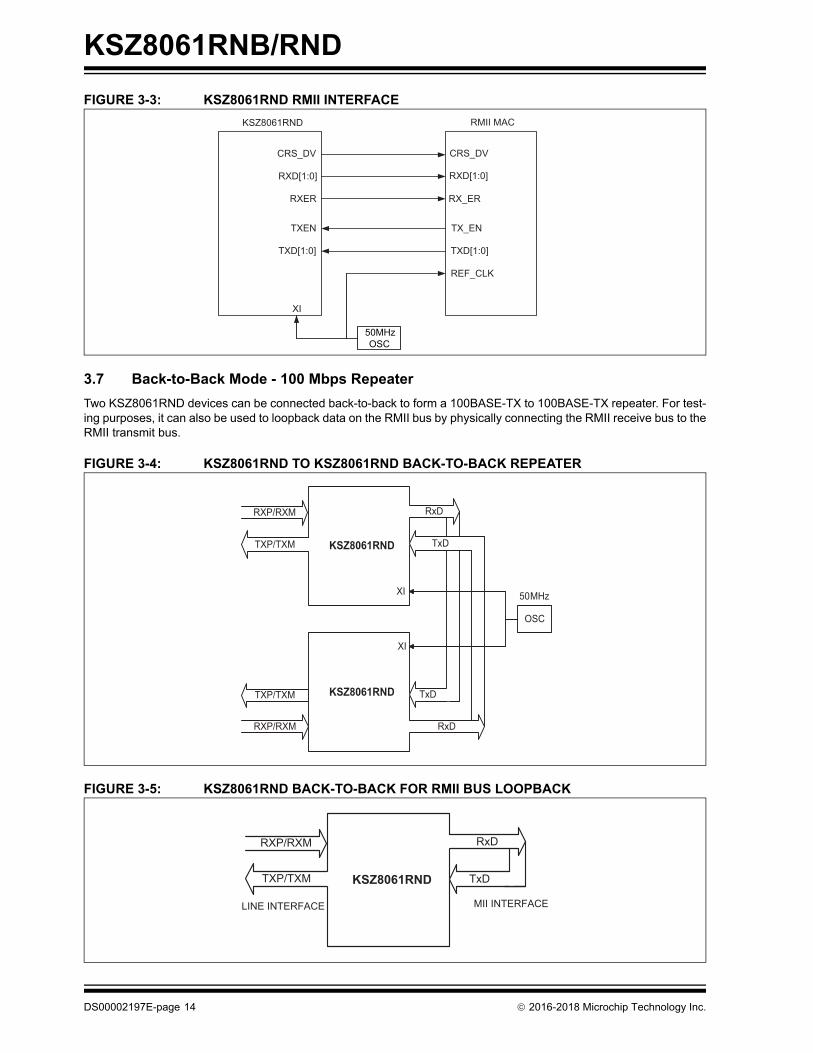
FIGURE 3-3: KSZ8061RND RMII INTERFACE
3.7 Back-to-Back Mode - 100 Mbps Repeater
Two KSZ8061RND devices can be connected back-to-back to form a 100BASE-TX to 100BASE-TX repeater. For test-ing purposes, it can also be used to loopback data on the RMII bus by physically connecting the RMII receive bus to theRMII transmit bus.
FIGURE 3-4: KSZ8061RND TO KSZ8061RND BACK-TO-BACK REPEATER
FIGURE 3-5: KSZ8061RND BACK-TO-BACK FOR RMII BUS LOOPBACK
KSZ8061RND
CRS_DV
RXD[1:0]
RXER
TXEN
RMII MAC
CRS_DV
RXD[1:0]
RX_ER
TX_EN
TXD[1:0] TXD[1:0]
REF_CLK
XI
50MHzOSC
KSZ8061RND
RXP/RXM
TXP/TXM
TXP/TXM
RXP/RXM
KSZ8061RND
RxD
TxD
RxD
TxD
OSC
XI
XI
50MHz
KSZ8061RND
RXP/RXM
TXP/TXM
RxD
TxD
MII INTERFACELINE INTERFACE
DS00002197E-page 14 2016-2018 Microchip Technology Inc.
KSZ8061RNB/RND
3.8 RMII Back-to-Back Mode
In RMII back-to-back mode, a KSZ8061RND interfaces with another KSZ8061RND to provide a complete 100-Mbpsrepeater solution.
The KSZ8061RND devices are configured to RMII Back-to-Back mode after power-up or reset with the following:
• Strapping pin CONFIG[2:0] set to ‘101’
• A common 50-MHz reference clock connected to XI of both KSZ8061RND devices
• RMII signals connected as shown in Table 3-2
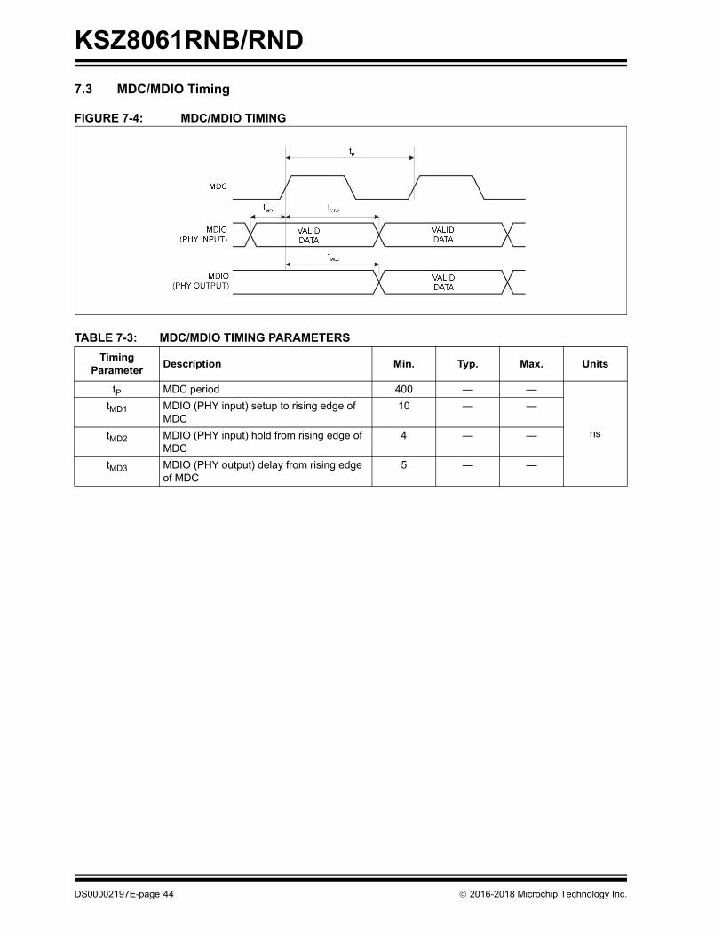
3.9 MII Management (MIIM) Interface
The KSZ8061RNB/RND supports the IEEE 802.3 MII Management Interface, also known as the Management DataInput/Output (MDIO) Interface. This interface enables an upper-layer device, like a MAC processor, to monitor and con-trol the state of the KSZ8061RNB/RND. An external device with MIIM capability is used to read the PHY status, or toconfigure the PHY settings, or both. Further details on the MIIM interface can be found in Clause 22.2.4 of the IEEE802.3 Specification.
The MIIM interface consists of the following:
• A physical connection that incorporates the clock line (MDC) and the data line (MDIO).
• A specific protocol that operates across the aforementioned physical connection that allows the external controller to communicate with one or more PHY devices.
• A set of 16-bit MDIO registers. Supported registers [0:8] are standard registers, and their functions are defined per the IEEE 802.3 specification. The additional registers are provided for expanded functionality. See “Register Map” section for details.
The KSZ8061RNB/RND supports unique PHY addresses 1 to 7, and broadcast PHY address 0. The broadcast addressis defined per the IEEE 802.3 specification, and can be used to write to multiple KSZ8061RNB/RND devices simultane-ously.
The PHYAD[2:0] strapping pins are used to assign a unique PHY address between 1 and 7 to each KSZ8061RNB/RNDdevice.
Table 3-3 shows the MII Management frame format.
3.10 LED Output Pins
The LED0 and LED1 pins indicate link status and is intended for driving LEDs. They are active low and can sink currentdirectly from the LEDs. By default, LED0 indicates Link/Activity, and LED1 indicates Link Speed. Bits [5:4] in register1Fh allow the definition of these pins to be changed to Link Status and Activity, respectively.
TABLE 3-2: RMII SIGNAL CONNECTION FOR RMII BACK-TO-BACK MODE
KSZ8061RND (100BASE-TX)[Device 1]
KSZ8061RND (100BASE-TX)[Device 1 or 2]
Pin Name Pin Type Pin Name Pin Type
CRS_DV OUTPUT TXEN INPUT
RXD1 OUTPUT TXD1 INPUT
RXD0 OUTPUT TXD0 INPUT
TXEN INPUT CRS_DV OUTPUT
TXD1 INPUT RXD1 OUTPUT
TXD0 INPUT RXD0 OUTPUT
TABLE 3-3: MII MANAGEMENT FRAME FORMAT
PreambleStart of Frame
Read/Write OP Code
PHY Address Bits [4:0]
REG Address Bits [4:0]
TAData
Bits [15:0]Idle
Read 32 1’s 01 10 00AAA RRRRR Z0 DDDDDDDD_DDDDDDDD Z
Write 32 1’s 01 01 00AAA RRRRR 10 DDDDDDDD_DDDDDDDD Z
2016-2018 Microchip Technology Inc. DS00002197E-page 15
KSZ8061RNB/RND
• Link Status: The LED indicates that the serial link is up.
• Link/Activity: When the link is up, but there is no traffic, the LED is on. When packets are being received or trans-mitted, the LED blinks.
• Activity: The LED blinks when packets are received or transmitted. It is off when there is no activity.
• Speed: When the link is up, the LED is on to indicate a 100BASE-TX link and is off to indicate a 10BASE-T link.
3.11 Interrupt (INTRP)
INTRP is an interrupt output signal that may be used to inform the external controller that there has been a status updateto the KSZ8061RNB/RND PHY register. This eliminates the need for the processor to poll the PHY for status changessuch as link up or down.
Register 1Bh, bits [15:8] are the interrupt control bits to enable and disable the conditions for asserting the INTRP signal.Register 1Bh, bits [7:0] are the interrupt status bits to indicate which interrupt conditions have occurred. The interruptstatus bits are cleared after reading register 1Bh.
Register 1Fh, bit [9] sets the interrupt level to active-high or active-low. The default is active-low.
3.12 HP Auto MDI/MDI-X
HP Auto MDI/MDI-X configuration eliminates the confusion of whether to use a straight cable or a crossover cablebetween the KSZ8061RNB/RND and its link partner. This feature allows the KSZ8061RNB/RND to use either type ofcable to connect with a link partner that is in either MDI or MDI-X mode. The auto-sense function detects transmit andreceive pairs from the link partner and then assigns transmit and receive pairs of the KSZ8061RNB/RND accordingly.
Auto MDI/MDI-X is initially enabled or disabled at hardware reset by hardware pin strapping (CONFIG[2:0]). Afterwards,it can be enabled or disabled by register 1Fh, bit [13]. When Auto MDI/MDI-X is disabled, serial data is normally trans-mitted on the pin pair TXP/TXM, and data is received on RXP/RXM. However, this may be reversed by writing to register1Fh, bit [14].
An isolation transformer with symmetrical transmit and receive data paths is recommended to support Auto MDI/MDI-X.
Table 3-4 illustrates how the IEEE 802.3 Standard defines MDI and MDI-X.
3.13 Straight Cable
A straight cable connects an MDI device to an MDI-X device, or an MDI-X device to an MDI device. Figure 3-6 depictsa typical straight cable connection between a NIC card (MDI device) and a switch, or hub (MDI-X device).
TABLE 3-4: MDI/MDI-X PIN DEFINITION
MDI MDI-X
RJ-45 Pin Signal RJ-45 Pin Signal
1 TX+ 1 RX+
2 TX– 2 RX–
3 RX+ 3 TX+
6 RX– 6 TX–
DS00002197E-page 16 2016-2018 Microchip Technology Inc.
KSZ8061RNB/RND
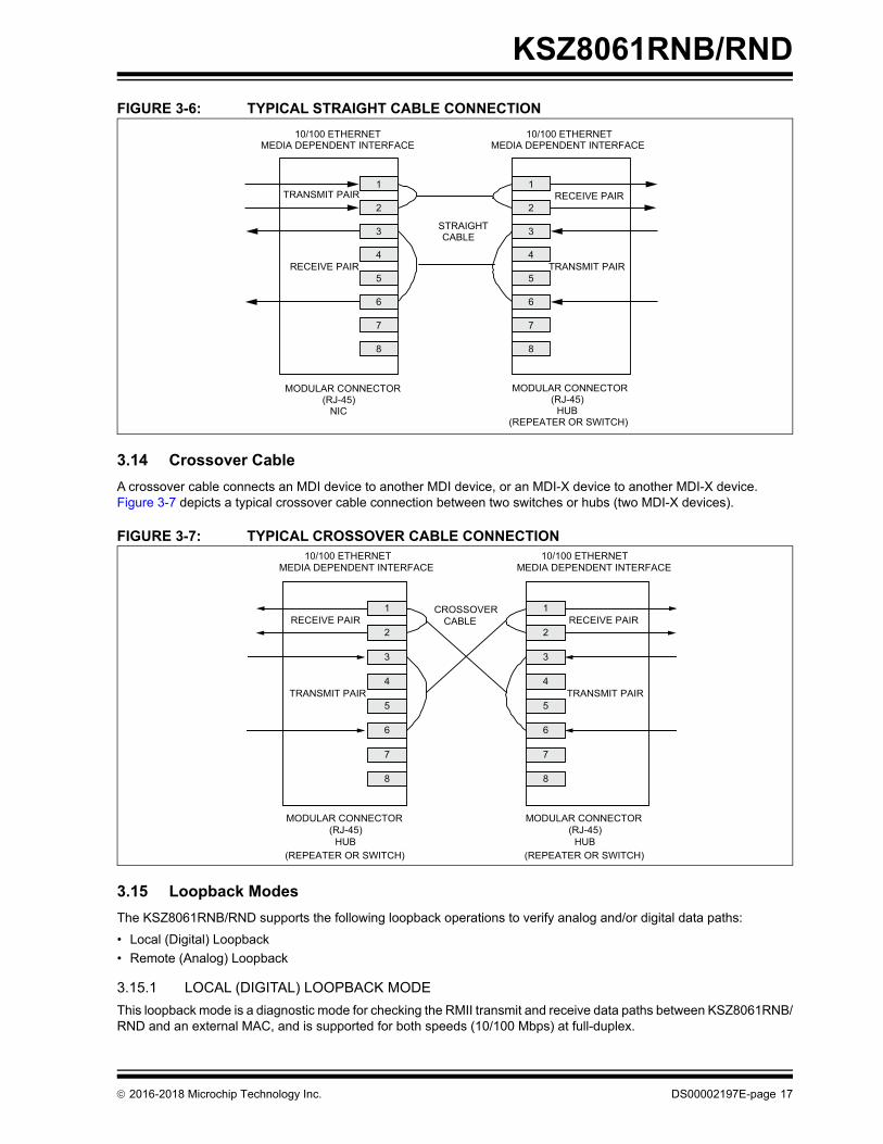
FIGURE 3-6: TYPICAL STRAIGHT CABLE CONNECTION
3.14 Crossover Cable
A crossover cable connects an MDI device to another MDI device, or an MDI-X device to another MDI-X device. Figure 3-7 depicts a typical crossover cable connection between two switches or hubs (two MDI-X devices).
FIGURE 3-7: TYPICAL CROSSOVER CABLE CONNECTION
3.15 Loopback Modes
The KSZ8061RNB/RND supports the following loopback operations to verify analog and/or digital data paths:
• Local (Digital) Loopback
• Remote (Analog) Loopback
3.15.1 LOCAL (DIGITAL) LOOPBACK MODE
This loopback mode is a diagnostic mode for checking the RMII transmit and receive data paths between KSZ8061RNB/RND and an external MAC, and is supported for both speeds (10/100 Mbps) at full-duplex.
RECEIVE PAIR TRANSMIT PAIR
RECEIVE PAIR
1
2
3
4
5
6
7
8
1 2 3 4 5 6 7 8
TRANSMIT PAIR
MODULAR CONNECTOR (RJ-45)
NIC
STRAIGHT CABLE
10/100 ETHERNET MEDIA DEPENDENT INTERFACE
10/100 ETHERNET MEDIA DEPENDENT INTERFACE
MODULAR CONNECTOR (RJ-45)
HUB(REPEATER OR SWITCH)
RECEIVE PAIR RECEIVE PAIR
TRANSMIT PAIR
1
2
3
4
5
6
7
8
1
2
3
4
5
6
7
8
TRANSMIT PAIR
10/100 ETHERNETMEDIA DEPENDENT INTERFACE
10/100 ETHERNETMEDIA DEPENDENT INTERFACE
MODULAR CONNECTOR (RJ-45)
HUB(REPEATER OR SWITCH)
CROSSOVERCABLE
MODULAR CONNECTOR (RJ-45)
HUB(REPEATER OR SWITCH)
2016-2018 Microchip Technology Inc. DS00002197E-page 17
KSZ8061RNB/RND
The loopback data path is shown in Figure 3-8.
1. RMII MAC transmits frames to KSZ8061RNB/RND.
2. Frames are wrapped around inside KSZ8061RNB/RND.
3. KSZ8061RNB/RND transmits frames back to RMII MAC.
FIGURE 3-8: LOCAL (DIGITAL) LOOPBACK
The following programming steps and register settings are used for Local Loopback mode.
This loopback mode checks the line (differential pairs, transformer, RJ-45 connector, Ethernet cable) transmit andreceive data paths between KSZ8061RNB/RND and its link partner, and is supported for 100BASE-TX full-duplex modeonly.
The loopback data path is shown in Figure 3-9.
• Fast Ethernet (100BASE-TX) PHY link partner transmits frames to KSZ8061RNB/RND.
• Frames are wrapped around inside KSZ8061RNB/RND.
• KSZ8061RNB/RND transmits frames back to fast Ethernet (100BASE-TX) PHY link partner.
RMIIMACRMII
PCS
(DIGITAL)
AFE
(ANALOG)
KSZ8061RNB/RND
DS00002197E-page 18 2016-2018 Microchip Technology Inc.
KSZ8061RNB/RND
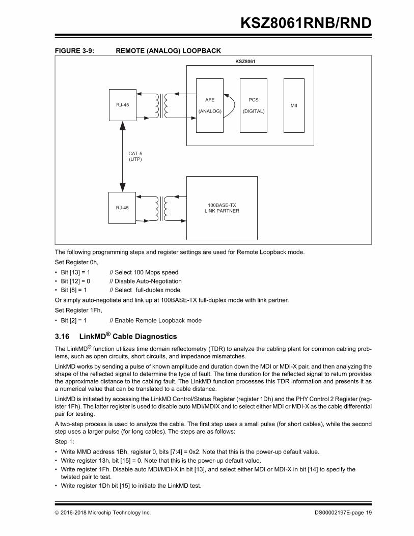
FIGURE 3-9: REMOTE (ANALOG) LOOPBACK
The following programming steps and register settings are used for Remote Loopback mode.
Set Register 0h,
• Bit [13] = 1 // Select 100 Mbps speed
• Bit [12] = 0 // Disable Auto-Negotiation
• Bit [8] = 1 // Select full-duplex mode
Or simply auto-negotiate and link up at 100BASE-TX full-duplex mode with link partner.
Set Register 1Fh,
• Bit [2] = 1 // Enable Remote Loopback mode
3.16 LinkMD® Cable Diagnostics
The LinkMD® function utilizes time domain reflectometry (TDR) to analyze the cabling plant for common cabling prob-lems, such as open circuits, short circuits, and impedance mismatches.
LinkMD works by sending a pulse of known amplitude and duration down the MDI or MDI-X pair, and then analyzing theshape of the reflected signal to determine the type of fault. The time duration for the reflected signal to return providesthe approximate distance to the cabling fault. The LinkMD function processes this TDR information and presents it asa numerical value that can be translated to a cable distance.
LinkMD is initiated by accessing the LinkMD Control/Status Register (register 1Dh) and the PHY Control 2 Register (reg-ister 1Fh). The latter register is used to disable auto MDI/MDIX and to select either MDI or MDI-X as the cable differentialpair for testing.
A two-step process is used to analyze the cable. The first step uses a small pulse (for short cables), while the secondstep uses a larger pulse (for long cables). The steps are as follows:
Step 1:
• Write MMD address 1Bh, register 0, bits [7:4] = 0x2. Note that this is the power-up default value.
• Write register 13h, bit [15] = 0. Note that this is the power-up default value.
• Write register 1Fh. Disable auto MDI/MDI-X in bit [13], and select either MDI or MDI-X in bit [14] to specify the twisted pair to test.
• Write register 1Dh bit [15] to initiate the LinkMD test.
RJ-45 MIIPCS
(DIGITAL)
AFE
(ANALOG)
KSZ8061
CAT-5(UTP)
RJ-45 100BASE-TXLINK PARTNER
2016-2018 Microchip Technology Inc. DS00002197E-page 19
KSZ8061RNB/RND
• Read register 1Dh to determine the result of the first step. Bit [15] = 0 indicates that the test is complete. After that, the result is read in bits [14:12]. Remember the result.
• Write register 1Dh bit [15] to initiate the LinkMD test.
• Read register 1Dh to determine the result of the first step. Bit [15] = 0 indicates that the test is complete. After that, the result is read in bits [14:12].
• If either step reveals a short, then there is a short. If either step reveals an open, then there is an open. If both tests indicate normal, then the cable is normal.
3.17 LinkMD®+ Enhanced Diagnostics: Receive Signal Quality Indicator
The KSZ8061RN provides a receive Signal Quality Indicator (SQI) feature, which indicates the relative quality of the100BASE-TX receive signal. It approximates a signal-to-noise ratio, and is affected by cable length, cable quality, andcoupled of environmental noise.
The raw SQI value is available for reading at any time from indirect register: MMD 1Ch, register ACh, bits [14:8]. A lowervalue indicates better signal quality, while a higher value indicates worse signal quality. Even in a stable configurationin a low-noise environment, the value read from this register may vary. The value should therefore be averaged by takingmultiple readings. The update interval of the SQI register is 2 µs, so measurements taken more frequently than 2 µs areredundant. In a quiet environment, 6 to 10 readings are suggested for averaging. In a noisy environment, individualreadings are unreliable, so a minimum of 30 readings are suggested for averaging. The SQI circuit does not include anyhysteresis.
Table 3-5 lists typical SQI values for various CAT5 cable lengths when linked to a typical 100BASE-TX device in a quietenvironment. In a noisy environment or during immunity testing, the SQI value increases.
3.18 NAND Tree Support
The KSZ8061RNB/RND provides parametric NAND tree support for fault detection between chip I/Os and board. TheNAND tree is a chain of nested NAND gates in which each KSZ8061RNB/RND digital I/O (NAND tree input) pin is aninput to one NAND gate along the chain. At the end of the chain, the CONFIG1 pin provides the output for the next NANDgates.
The NAND tree test process includes:
• Enabling NAND tree mode
• Pulling all NAND tree input pins high
• Driving low each NAND tree input pin sequentially per the NAND tree pin order
• Checking the NAND tree output to ensure there is a toggle high-to-low or low-to-high for each NAND tree input driven low
DS00002197E-page 20 2016-2018 Microchip Technology Inc.
KSZ8061RNB/RND
Table 3-6 lists the NAND tree pin order.
3.19 NAND Tree I/O Testing
The following procedure can be used to check for faults on the KSZ8061RNB/RND digital I/O pin connections to theboard:
1. Enable NAND tree mode by INTRP pin strapping option.
2. Use board logic to drive all KSZ8061RNB/RND NAND tree input pins high.
3. Use board logic to drive each NAND tree input pin, per KSZ8061RNB/RND NAND Tree pin order, as follows:
a) Toggle the first pin (MDIO) from high to low, and verify the CONFIG1 pin switch from high to low to indicatethat the first pin is connected properly.
b) Leave the first pin (MDIO) low.
c) Toggle the second pin (MDC) from high to low, and verify the CONFIG1 pin switch from low to high to indicatethat the second pin is connected properly.
d) Leave the first pin (MDIO) and the second pin (MDC) low.
e) Toggle the third pin (RXER) from high to low, and verify the CONFIG1 pin switch from high to low to indicatethat the third pin is connected properly.
f) Continue with this sequence until all KSZ8061RNB/RND NAND tree input pins have been toggled.
Each KSZ8061RNB/RND NAND tree input pin must cause the CONFIG1 output pin to toggle high-to-low or low-to-highto indicate a good connection. If the CONFIG1 pin fails to toggle when the KSZ8061RNB/RND input pin toggles fromhigh to low, the input pin has a fault.
TABLE 3-6: KSZ8061RNB/RNDNAND TREE TEST PIN ORDER
Pin Number Pin Name NAND Tree Description
10 MDIO INPUT
11 MDC INPUT
12 RXER INPUT
13 CRS_DV INPUT
14 PHYAD0 INPUT
16 PHYAD1 INPUT
17 RXD1 INPUT
18 RXD0 INPUT
19 REF_CLK INPUT
20 DNU INPUT
21 TXEN INPUT
22 TXD0 INPUT
23 TXD1 INPUT
24 LED0 INPUT
25 DNU INPUT
26 DNU INPUT
29 INTRP INPUT
27 CONFIG OUTPUT
2016-2018 Microchip Technology Inc. DS00002197E-page 21
KSZ8061RNB/RND
3.20 Power Management
The KSZ8061RNB/RND offers the following power management modes which are enabled and disabled by registercontrol.
3.20.1 POWER SAVING MODE
Power Saving mode is used to reduce the transceiver power consumption when the cable is unplugged. This mode doesnot interfere with normal device operation. It is enabled by writing a one to register 1Fh, bit [10], and is in effect whenauto-negotiation mode is enabled and the cable is disconnected (no link). In this mode, the KSZ8061RNB/RND shutsdown all transceiver blocks except for the transmitter, energy detect, and PLL circuits. By default, Power Saving modeis disabled after power-up.
3.20.2 ENERGY-DETECT POWER-DOWN MODE
Energy-Detect Power-Down (EDPD) mode is used to further reduce the transceiver power consumption when the cableis unplugged, relative to Power Saving mode. This mode does not interfere with normal device operation. It is enabledby writing a zero to register 18h, bit [11], and is in effect when auto-negotiation mode is enabled and cable is discon-nected (no link).
EDPD mode can be optionally enhanced with a PLL Off feature, which turns off all KSZ8061RNB/RND transceiverblocks, except for transmitter and energy detect circuits. PLL Off is set by writing a one to register 10h, bit [4].
Further power reduction is achieved by extending the time interval in between transmissions of link pulses while in thismode. The periodic transmission of link pulses is needed to ensure two link partners in the same low powered state withauto MDI/MDI-X disabled can wake up when the cable is connected between them.
By default, EDPD mode is disabled after power-up.
3.20.3 POWER-DOWN MODE
Power-Down mode is used to power down the KSZ8061RNB/RND when it is not in use after power-up. It is enabled bywriting a one to register 0h, bit [11].
In this mode, the KSZ8061RNB/RND disables all internal functions except the MII management interface. TheKSZ8061RNB/RND exits (disables) the Power-Down mode after register 0h, bit [11] is set back to zero.
3.20.4 SLOW OSCILLATOR MODE
Slow Oscillator mode is used to disconnect the input reference crystal/clock on XI (pin 1) and select the on-chip slowoscillator when the KSZ8061RNB/RND is not in use after power-up. It is enabled by writing a one to register 11h, bit [6].
Slow Oscillator mode works in conjunction with Power-Down mode to put the KSZ8061RNB/RND into a lower powerstate with all internal functions disabled, except for the MII management interface. To properly exit this mode and returnto normal PHY operation, use the following programming sequence:
1. Disable Slow Oscillator mode by writing a zero to register 11h, bit [6].
2. Disable Power-Down mode by writing a zero to register 0h, bit [11].
3. Initiate software reset by writing a one to register 0h, bit [15].
3.20.5 ULTRA-DEEP SLEEP MODE
Ultra-Deep Sleep mode is used to achieve the lowest possible power consumption while retaining the ability to detectactivity on the Tx/Rx cable pairs, and is intended for achieving negligible battery drain during long periods of inactivity.It is controlled by several register bits, and Ultra-Deep Sleep mode may be entered by writing to a register, or it may beinitiated automatically when Signal Detect (SIGDET) is deasserted. Details are given in the Signal Detect (SIGDET) andUltra-Deep Sleep mode section.
In Ultra-Deep Sleep mode, the KSZ8061RNB/RND disables all internal functions and I/Os except for the ultra-low powersignal detect circuit and the Signal Detect pin (SIGDET), which are powered from VDDIO. For lowest power consump-tion, the 1.2V supply (VDDL and AVDDL) may be turned off externally. Hardware reset is required to exit Ultra-DeepSleep mode.
DS00002197E-page 22 2016-2018 Microchip Technology Inc.
KSZ8061RNB/RND
3.20.6 NON-VOLATILE REGISTERS
Most of the logic circuitry of the KSZ8061RNB/RND, including the status and control registers, is powered by the 1.2Vsupply. When the 1.2V supply is turned off in Ultra-Deep Sleep mode, the content of the registers is lost. Because of theimportance of register 14h and bit [0] of register 13h, which control the various power modes, these bits are duplicatedin a logic block powered by the 3.3V supply. These register bits are therefore “non-volatile” while in Ultra-Deep Sleepmode.
To access the non-volatile (3.3V) registers, bit [4] of register 14h must first be set. Otherwise, writes to these registersmodify only the volatile versions of these registers, and not the non-volatile versions.
3.21 Signal Detect (SIGDET) and Ultra-Deep Sleep Mode
SIGDET is an output signal which may be used for power reduction, either by directly turning off selected power or bysignaling to a host controller when no signal is detected on the line interface. It is asserted when sufficient energy isdetected on either of the differential pairs, and is deasserted when cable energy is not detected. The signal detectioncircuit consumes almost no power from the VDDIO supply, and does not use the 1.2V supply at all.
Ultra-Deep Sleep mode may be entered either automatically in unison with the Signal Detect signal (Automatic method),or manually by setting a register bit (CPU Control method).
The signal detect feature and Ultra-Deep Sleep mode are controlled via multiple bits in register 14h:
• Register 14h, bit [6] Ultra-Deep Sleep method: either Automatic or CPU Control
• Register 14h, bit [5] Manually enter Ultra Deep Sleep mode when CPU Control method is selected
• Register 14h, bit [4] Enable R/W access to non-volatile versions of register 14h and bits [9:8] and [1:0] ofregister 13h. Set this bit when bit [3] is set.
• Register 14h, bit [3] Enable Ultra Deep Sleep Mode and SIGDET
• Register 14h, bit [1] Extend timing for SIGDET deassertion and entry into Ultra-Deep Sleep mode
• Register 14h, bit [0] SIGDET output polarity
3.21.1 CPU CONTROL METHOD (MIIM INTERFACE)
• KSZ8061RNB/RND drives SIGDET signal to the CPU.
• SIGDET defaults to force high, to not interfere with PHY initialization by the CPU. At power-on, the KSZ8061RNB/RND drives SIGDET high, without consideration of cable energy level.
• During initialization, the CPU writes data 0x0058 to register 14h.
- Bit [4] enables access to the non-volatile copy of register 14h.
- Enable Ultra-Deep Sleep mode and SIGDET by setting register 14h, bit [3].
- Automatic Ultra-Deep Sleep functionality is disabled by setting register 14h, bit [6].
• SIGDET is now enabled and changes state as cable energy changes.
• In response to the deassertion of SIGDET, the CPU puts KSZ8061RNB/RND into Ultra-Deep Sleep mode by set-ting register 14h, bit [5]. To further reduce power, the CPU may disable the 1.2V supply to the KSZ8061RNB/RND.
• The KSZ8061RNB/RND asserts SIGDET when energy is detected on the cable.
• To activate the KSZ8061RNB/RND, the CPU enables the 1.2V supply and asserts hardware reset (RESET#) to the KSZ8061RNB/RND. Because the KSZ8061RNB/RND is completely reset, the registers must be re-initialized.
• Alternately, it is possible to maintain register access during Ultra-Deep Sleep mode by preserving the 1.2V power supply and setting register 13h, bit [0] to enable slow oscillator mode. Ultra-Deep Sleep mode can then be exited by writing to register 14h. The 1.2V supply results in increased power consumption.
3.21.2 AUTOMATIC STANDBY METHOD
• The board may be designed such that the KSZ8061RNB/RND SIGDET signal enables the 1.2V power supply to KSZ8061RNB/RND.
• At power-on, the KSZ8061RNB/RND drives SIGDET high, without consideration of cable energy level.
• During initialization, CPU writes data 0x001A or 0x0018 to register 14h.
- Bit [4] enables access to the non-volatile copy of register 14h.
- Enable Ultra-Deep Sleep mode and SIGDET by setting register 14h, bit [3].
- Automatic Ultra-Deep Sleep functionality is enabled by clearing register 14h, bit [6].
- SIGDET timing bit [1] must be set unless the link partner is not using auto-negotiation, auto-MDI/MDI-X is dis-
2016-2018 Microchip Technology Inc. DS00002197E-page 23
KSZ8061RNB/RND
abled, and link is at 100 Mbps.
• When the KSZ8061RNB/RND detects signal loss, it automatically enters Ultra-Deep Sleep mode and deasserts SIGDET. SIGDET may be used to disable the 1.2V supply.
• When the KSZ8061RNB/RND detects a signal, it asserts SIGDET (which enables the 1.2V supply) and automati-cally wakes up. SIGDET may be used to wake up the CPU, which then re-initializes the KSZ8061RNB/RND.
• Alternatively, a hardware reset (RESET#) brings the KSZ8061RNB/RND out of Ultra-Deep Sleep mode.
• The contents of register 14h and bits [9:8] and [1:0] of register 13h are preserved during Ultra-Deep Sleep mode, but are lost during hardware reset.
DS00002197E-page 24 2016-2018 Microchip Technology Inc.
KSZ8061RNB/RND
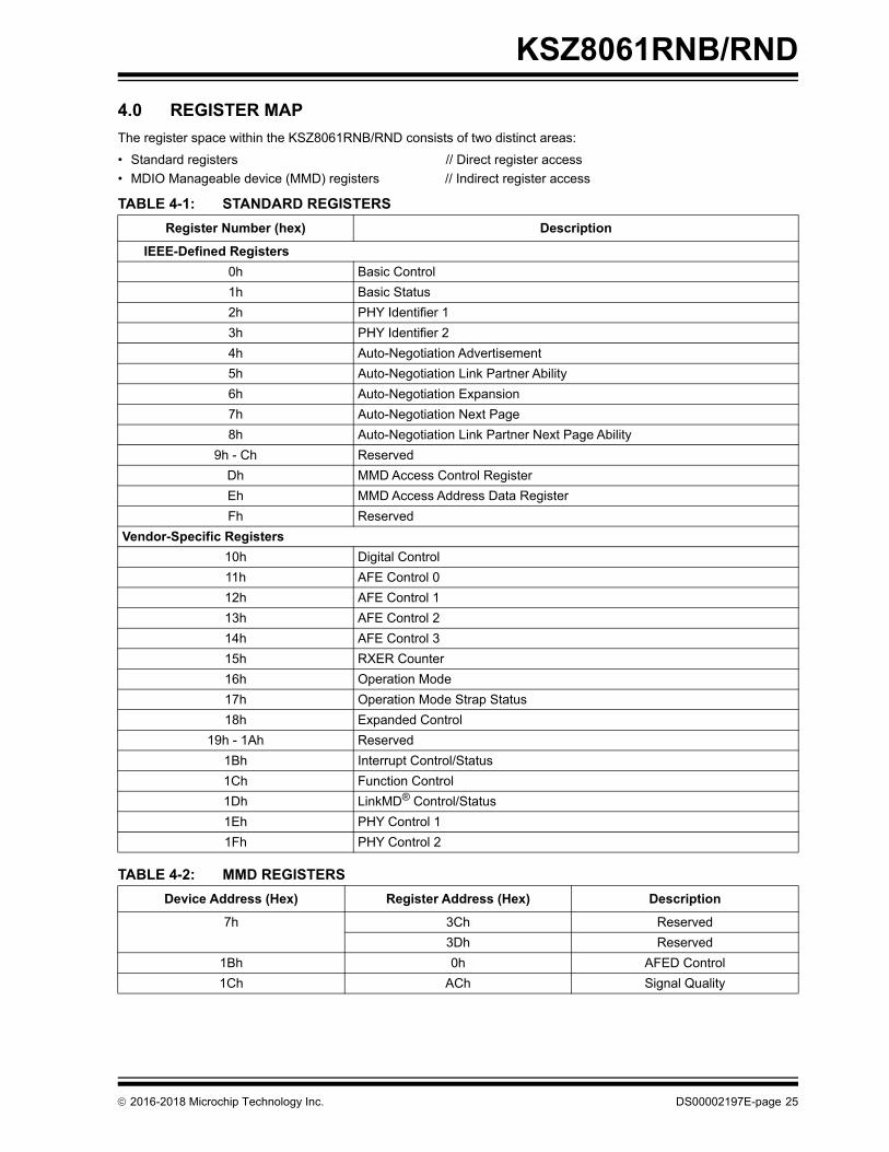
4.0 REGISTER MAP
The register space within the KSZ8061RNB/RND consists of two distinct areas:
2016-2018 Microchip Technology Inc. DS00002197E-page 25
KSZ8061RNB/RND
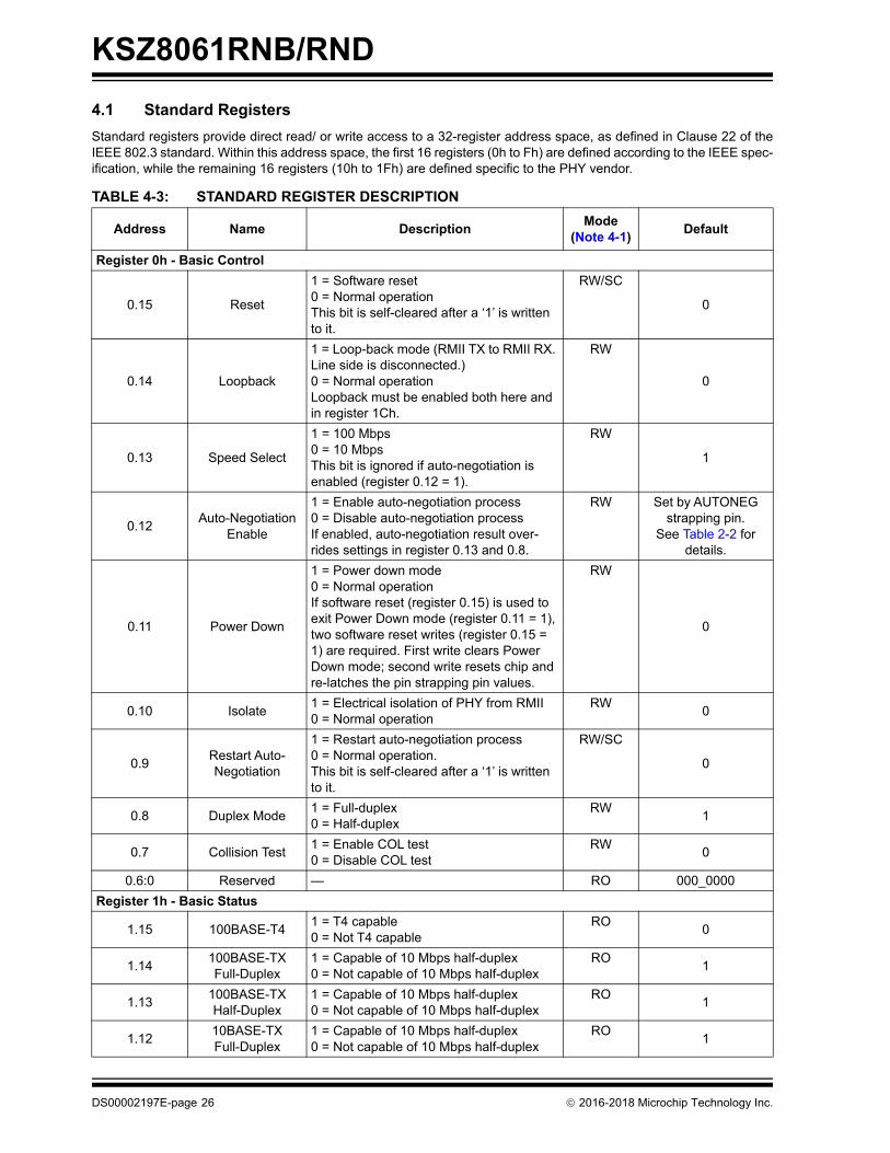
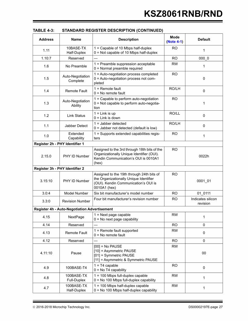
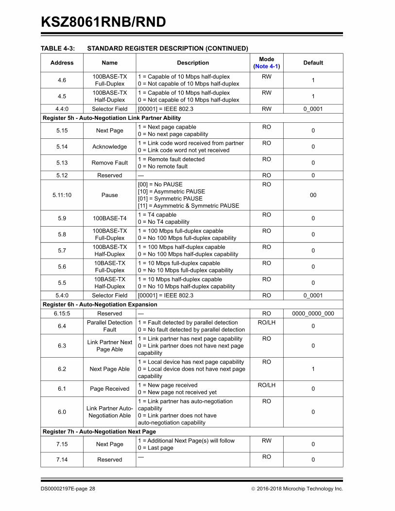
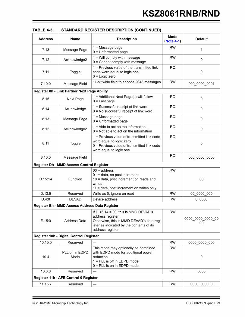
4.1 Standard Registers
Standard registers provide direct read/ or write access to a 32-register address space, as defined in Clause 22 of theIEEE 802.3 standard. Within this address space, the first 16 registers (0h to Fh) are defined according to the IEEE spec-ification, while the remaining 16 registers (10h to 1Fh) are defined specific to the PHY vendor.
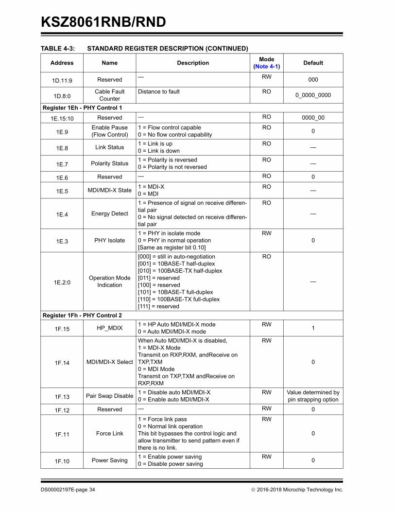
TABLE 4-3: STANDARD REGISTER DESCRIPTION
Address Name DescriptionMode
(Note 4-1)Default
Register 0h - Basic Control
0.15 Reset
1 = Software reset0 = Normal operationThis bit is self-cleared after a ‘1’ is written to it.
RW/SC
0
0.14 Loopback
1 = Loop-back mode (RMII TX to RMII RX. Line side is disconnected.)0 = Normal operationLoopback must be enabled both here and in register 1Ch.
RW
0
0.13 Speed Select
1 = 100 Mbps0 = 10 MbpsThis bit is ignored if auto-negotiation is enabled (register 0.12 = 1).
RW
1
0.12Auto-Negotiation
Enable
1 = Enable auto-negotiation process0 = Disable auto-negotiation processIf enabled, auto-negotiation result over-rides settings in register 0.13 and 0.8.
RW Set by AUTONEG strapping pin.
See Table 2-2 for details.
0.11 Power Down
1 = Power down mode0 = Normal operationIf software reset (register 0.15) is used to exit Power Down mode (register 0.11 = 1), two software reset writes (register 0.15 = 1) are required. First write clears Power Down mode; second write resets chip and re-latches the pin strapping pin values.
RW
0
0.10 Isolate1 = Electrical isolation of PHY from RMII0 = Normal operation
RW0
0.9Restart Auto-Negotiation
1 = Restart auto-negotiation process0 = Normal operation.This bit is self-cleared after a ‘1’ is written to it.
RW/SC
0
0.8 Duplex Mode1 = Full-duplex0 = Half-duplex
RW1
0.7 Collision Test1 = Enable COL test0 = Disable COL test
RW0
0.6:0 Reserved — RO 000_0000
Register 1h - Basic Status
1.15 100BASE-T41 = T4 capable0 = Not T4 capable
RO0
1.14100BASE-TX Full-Duplex
1 = Capable of 10 Mbps half-duplex0 = Not capable of 10 Mbps half-duplex
RO1
1.13100BASE-TX Half-Duplex
1 = Capable of 10 Mbps half-duplex0 = Not capable of 10 Mbps half-duplex
RO1
1.1210BASE-TX Full-Duplex
1 = Capable of 10 Mbps half-duplex0 = Not capable of 10 Mbps half-duplex
RO1
DS00002197E-page 26 2016-2018 Microchip Technology Inc.
KSZ8061RNB/RND
1.1110BASE-TX Half-Duplex
1 = Capable of 10 Mbps half-duplex0 = Not capable of 10 Mbps half-duplex
RO1
1.10:7 Reserved — RO 000_0
1.6 No Preamble1 = Preamble suppression acceptable0 = Normal preamble required
RW1
1.5Auto-Negotiation
Complete
1 = Auto-negotiation process completed0 = Auto-negotiation process not com-pleted
RO0
1.4 Remote Fault1 = Remote fault0 = No remote fault
RO/LH0
1.3Auto-Negotiation
Ability
1 = Capable to perform auto-negotiation0 = Not capable to perform auto-negotia-tion
RO1
1.2 Link Status1 = Link is up0 = Link is down
RO/LL0
1.1 Jabber Detect1 = Jabber detected0 = Jabber not detected (default is low)
RO/LH0
1.0Extended Capability
1 = Supports extended capabilities regis-ters
RO1
Register 2h - PHY Identifier 1
2.15.0 PHY ID Number
Assigned to the 3rd through 18th bits of the Organizationally Unique Identifier (OUI). Kendin Communication’s OUI is 0010A1 (hex)
RO
0022h
Register 3h - PHY Identifier 2
3.15:10 PHY ID Number
Assigned to the 19th through 24th bits of the Organizationally Unique Identifier (OUI). Kendin Communication’s OUI is 0010A1 (hex)
RO
0001_01
3.0:4 Model Number Six bit manufacturer’s model number RO 01_0111
3.3:0 Revision NumberFour bit manufacturer’s revision number RO Indicates silicon
revision
Register 4h - Auto-Negotiation Advertisement
4.15 NextPage1 = Next page capable0 = No next page capability
8.12 Acknowledge21 = Able to act on the information0 = Not able to act on the information
RO0
8.11 Toggle
1 = Previous value of transmitted link code word equal to logic zero0 = Previous value of transmitted link code word equal to logic one
RO
0
8.10:0 Message Field — RO 000_0000_0000
Register Dh - MMD Access Control Register
D.15:14 Function
00 = address01 = data, no post increment10 = data, post increment on reads and writes11 = data, post increment on writes only
RW
00
D.13:5 Reserved Write as 0, ignore on read RW 00_0000_000
D.4:0 DEVAD Device address RW 0_0000
Register Eh - MMD Access Address Data Register
E.15:0 Address Data
If D.15:14 = 00, this is MMD DEVAD’s address register.Otherwise, this is MMD DEVAD’s data reg-ister as indicated by the contents of its address register.
RW
0000_0000_0000_0000
Register 10h - Digital Control Register
10.15:5 Reserved — RW 0000_0000_000
10.4PLL off in EDPD
Mode
This mode may optionally be combined with EDPD mode for additional power reduction.1 = PLL is off in EDPD mode0 = PLL is on in EDPD mode
RW
0
10.3:0 Reserved — RW 0000
Register 11h - AFE Control 0 Register
11.15:7 Reserved — RW 0000_0000_0
TABLE 4-3: STANDARD REGISTER DESCRIPTION (CONTINUED)
Address Name DescriptionMode
(Note 4-1)Default
2016-2018 Microchip Technology Inc. DS00002197E-page 29
KSZ8061RNB/RND
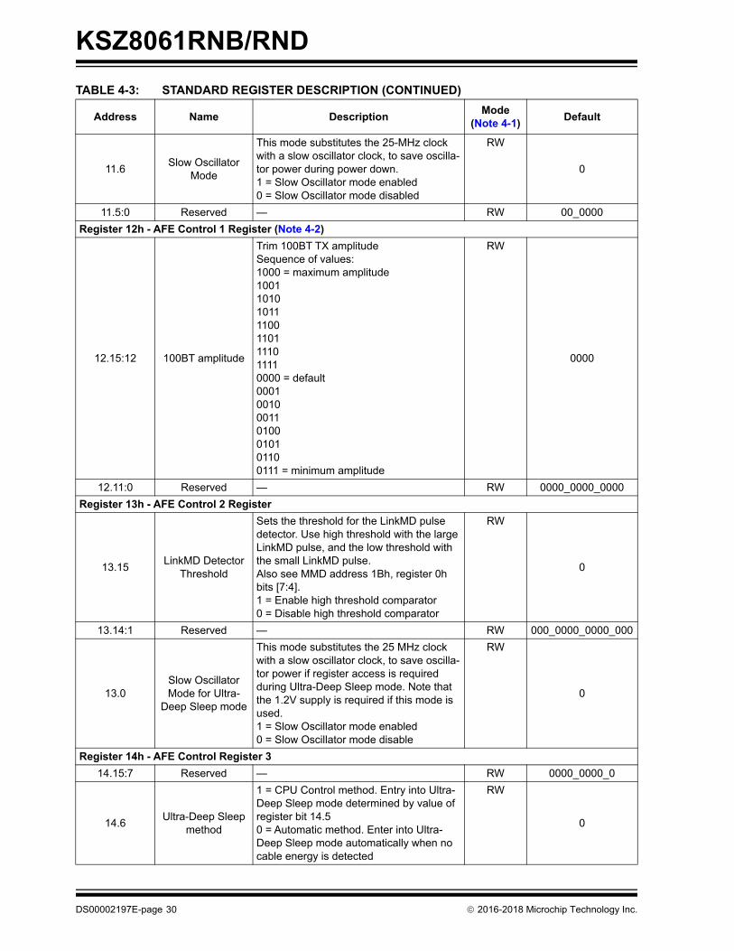
11.6Slow Oscillator
Mode
This mode substitutes the 25-MHz clock with a slow oscillator clock, to save oscilla-tor power during power down.1 = Slow Oscillator mode enabled0 = Slow Oscillator mode disabled
RW
0
11.5:0 Reserved — RW 00_0000
Register 12h - AFE Control 1 Register (Note 4-2)
12.15:12 100BT amplitude
Trim 100BT TX amplitudeSequence of values:1000 = maximum amplitude10011010101111001101111011110000 = default0001001000110100010101100111 = minimum amplitude
RW
0000
12.11:0 Reserved — RW 0000_0000_0000
Register 13h - AFE Control 2 Register
13.15LinkMD Detector
Threshold
Sets the threshold for the LinkMD pulse detector. Use high threshold with the large LinkMD pulse, and the low threshold with the small LinkMD pulse.Also see MMD address 1Bh, register 0h bits [7:4].1 = Enable high threshold comparator0 = Disable high threshold comparator
RW
0
13.14:1 Reserved — RW 000_0000_0000_000
13.0Slow Oscillator Mode for Ultra-
Deep Sleep mode
This mode substitutes the 25 MHz clock with a slow oscillator clock, to save oscilla-tor power if register access is required during Ultra-Deep Sleep mode. Note that the 1.2V supply is required if this mode is used.1 = Slow Oscillator mode enabled0 = Slow Oscillator mode disable
RW
0
Register 14h - AFE Control Register 3
14.15:7 Reserved — RW 0000_0000_0
14.6Ultra-Deep Sleep
method
1 = CPU Control method. Entry into Ultra-Deep Sleep mode determined by value of register bit 14.50 = Automatic method. Enter into Ultra-Deep Sleep mode automatically when no cable energy is detected
RW
0
TABLE 4-3: STANDARD REGISTER DESCRIPTION (CONTINUED)
Address Name DescriptionMode
(Note 4-1)Default
DS00002197E-page 30 2016-2018 Microchip Technology Inc.
KSZ8061RNB/RND
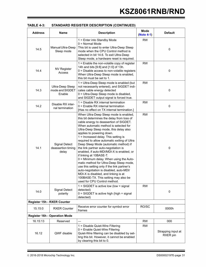
14.5Manual Ultra-Deep
Sleep mode
1 = Enter into Standby Mode0 = Normal ModeThis bit is used to enter Ultra-Deep Sleep mode when the CPU Control method is selected in bit 14.6. To exit Ultra-Deep Sleep mode, a hardware reset is required.
RW
0
14.4NV Register
Access
1 = Enable the non-volatile copy of register 14h and bits [9:8] and [1:0] of 13h.0 = Disable access to non-volatile registersWhen Ultra-Deep Sleep mode is enabled, this bit must be set to 1.
RW
0
14.3Ultra-Deep Sleep
mode and SIGDET Enable
1 = Ultra-Deep Sleep mode is enabled (but not necessarily entered), and SIGDET indi-cates cable energy detected0 = Ultra-Deep Sleep mode is disabled, and SIGDET output signal is forced true.
RW
0
14.2Disable RX inter-nal termination
1 = Disable RX internal termination0 = Enable RX internal termination[Has no effect on TX internal termination.]
RW0
14.1Signal Detect
deassertion timing delay
When Ultra-Deep Sleep mode is enabled, this bit determines the delay from loss of cable energy to deassertion of SIGDET. When automatic method is selected for Ultra-Deep Sleep mode, this delay also applies to powering down.1 = Increased delay. This setting is required to allow automatic exiting of Ultra Deep Sleep Mode (automatic method) if the link partner auto-negotiation is enabled, if auto-MDI/MDI-X is enabled, or if linking at 10BASE-T.0 = Minimum delay. When using the Auto-matic method for Ultra-Deep Sleep mode, use this setting only if the link partner’s auto-negotiation is disabled, auto-MDI/MDI-X is disabled, and linking is at 100BASE-TX. This setting may also be used for CPU Control method.
RW
0
14.0Signal Detect
polarity
1 = SIGDET is active low (low = signal detected)0 = SIGDET is active high (high = signal detected)
RW
0
Register 15h - RXER Counter
15.15:0 RXER CounterReceive error counter for symbol error frames
RO/SC0000h
Register 16h - Operation Mode
16.15:13 Reserved — RW 000
16.12 QWF disable
1 = Disable Quiet-Wire Filtering0 = Enable Quiet-Wire FilteringQuiet-Wire filtering can be disabled by set-ting this bit. However, it cannot be enabled by clearing this bit to 0.
RW
Strapping input at RXER pin
TABLE 4-3: STANDARD REGISTER DESCRIPTION (CONTINUED)
Address Name DescriptionMode
(Note 4-1)Default
2016-2018 Microchip Technology Inc. DS00002197E-page 31
KSZ8061RNB/RND
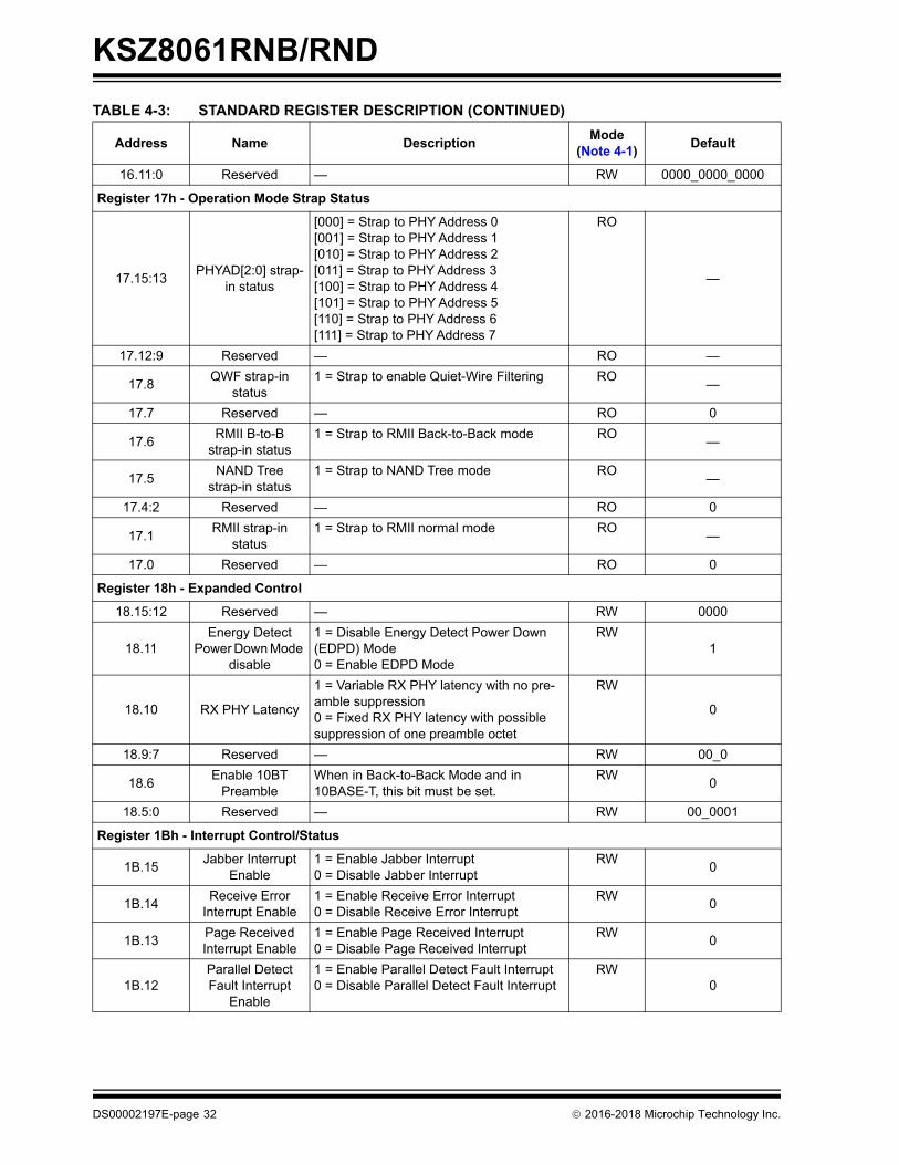
16.11:0 Reserved — RW 0000_0000_0000
Register 17h - Operation Mode Strap Status
17.15:13PHYAD[2:0] strap-
in status
[000] = Strap to PHY Address 0[001] = Strap to PHY Address 1[010] = Strap to PHY Address 2[011] = Strap to PHY Address 3[100] = Strap to PHY Address 4[101] = Strap to PHY Address 5[110] = Strap to PHY Address 6[111] = Strap to PHY Address 7
RO
—
17.12:9 Reserved — RO —
17.8QWF strap-in
status1 = Strap to enable Quiet-Wire Filtering RO
—
17.7 Reserved — RO 0
17.6RMII B-to-B
strap-in status1 = Strap to RMII Back-to-Back mode RO
—
17.5NAND Tree
strap-in status1 = Strap to NAND Tree mode RO
—
17.4:2 Reserved — RO 0
17.1RMII strap-in
status1 = Strap to RMII normal mode RO
—
17.0 Reserved — RO 0
Register 18h - Expanded Control
18.15:12 Reserved — RW 0000
18.11Energy Detect
Power Down Mode disable
1 = Disable Energy Detect Power Down (EDPD) Mode0 = Enable EDPD Mode
RW1
18.10 RX PHY Latency
1 = Variable RX PHY latency with no pre-amble suppression0 = Fixed RX PHY latency with possible suppression of one preamble octet
RW
0
18.9:7 Reserved — RW 00_0
18.6Enable 10BT
PreambleWhen in Back-to-Back Mode and in 10BASE-T, this bit must be set.
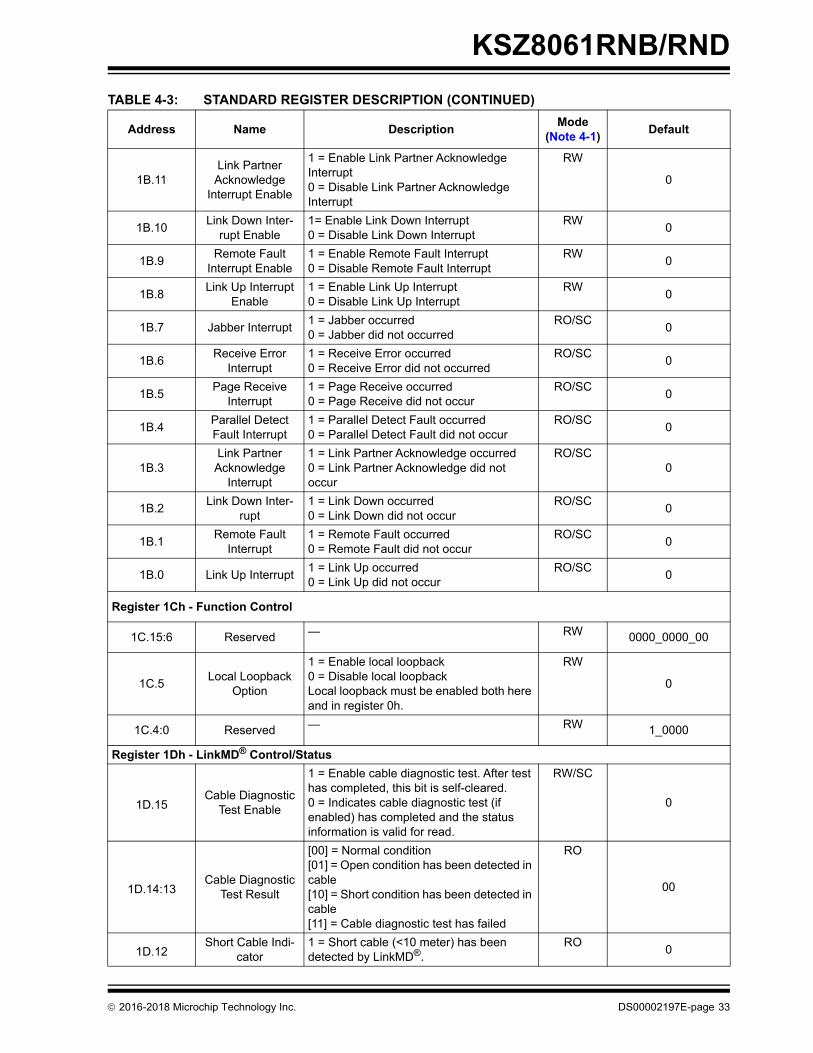
Enable1 = Enable Link Up Interrupt0 = Disable Link Up Interrupt
RW0
1B.7 Jabber Interrupt1 = Jabber occurred0 = Jabber did not occurred
RO/SC0
1B.6Receive Error
Interrupt1 = Receive Error occurred0 = Receive Error did not occurred
RO/SC0
1B.5Page Receive
Interrupt1 = Page Receive occurred0 = Page Receive did not occur
RO/SC0
1B.4Parallel Detect Fault Interrupt
1 = Parallel Detect Fault occurred0 = Parallel Detect Fault did not occur
RO/SC0
1B.3Link Partner Acknowledge
Interrupt
1 = Link Partner Acknowledge occurred0 = Link Partner Acknowledge did not occur
RO/SC0
1B.2Link Down Inter-
rupt1 = Link Down occurred0 = Link Down did not occur
RO/SC0
1B.1Remote Fault
Interrupt1 = Remote Fault occurred0 = Remote Fault did not occur
RO/SC0
1B.0 Link Up Interrupt1 = Link Up occurred0 = Link Up did not occur
RO/SC0
Register 1Ch - Function Control
1C.15:6 Reserved — RW 0000_0000_00
1C.5Local Loopback
Option
1 = Enable local loopback0 = Disable local loopbackLocal loopback must be enabled both here and in register 0h.
RW
0
1C.4:0 Reserved — RW 1_0000
Register 1Dh - LinkMD® Control/Status
1D.15Cable Diagnostic
Test Enable
1 = Enable cable diagnostic test. After test has completed, this bit is self-cleared.0 = Indicates cable diagnostic test (if enabled) has completed and the status information is valid for read.
RW/SC
0
1D.14:13Cable Diagnostic
Test Result
[00] = Normal condition[01] = Open condition has been detected in cable[10] = Short condition has been detected in cable[11] = Cable diagnostic test has failed
RO
00
1D.12Short Cable Indi-
cator1 = Short cable (<10 meter) has been detected by LinkMD®.
RO0
TABLE 4-3: STANDARD REGISTER DESCRIPTION (CONTINUED)
Address Name DescriptionMode
(Note 4-1)Default
2016-2018 Microchip Technology Inc. DS00002197E-page 33
KSZ8061RNB/RND
1D.11:9 Reserved — RW 000
1D.8:0Cable Fault
CounterDistance to fault RO
0_0000_0000
Register 1Eh - PHY Control 1
1E.15:10 Reserved — RO 0000_00
1E.9Enable Pause (Flow Control)
1 = Flow control capable0 = No flow control capability
RO0
1E.8 Link Status1 = Link is up0 = Link is down
RO—
1E.7 Polarity Status1 = Polarity is reversed0 = Polarity is not reversed
RO—
1E.6 Reserved — RO 0
1E.5 MDI/MDI-X State1 = MDI-X0 = MDI
RO—
1E.4 Energy Detect
1 = Presence of signal on receive differen-tial pair0 = No signal detected on receive differen-tial pair
RO
—
1E.3 PHY Isolate1 = PHY in isolate mode0 = PHY in normal operation[Same as register bit 0.10]
1F.15 HP_MDIX1 = HP Auto MDI/MDI-X mode0 = Auto MDI/MDI-X mode
RW1
1F.14 MDI/MDI-X Select
When Auto MDI/MDI-X is disabled,1 = MDI-X ModeTransmit on RXP,RXM, andReceive on TXP,TXM 0 = MDI ModeTransmit on TXP,TXM andReceive on RXP,RXM
RW
0
1F.13 Pair Swap Disable1 = Disable auto MDI/MDI-X0 = Enable auto MDI/MDI-X
RW Value determined by pin strapping option
1F.12 Reserved — RW 0
1F.11 Force Link
1 = Force link pass0 = Normal link operationThis bit bypasses the control logic and allow transmitter to send pattern even if there is no link.
RW
0
1F.10 Power Saving1 = Enable power saving 0 = Disable power saving
RW0
TABLE 4-3: STANDARD REGISTER DESCRIPTION (CONTINUED)
Address Name DescriptionMode
(Note 4-1)Default
DS00002197E-page 34 2016-2018 Microchip Technology Inc.
KSZ8061RNB/RND
4.2 MMD Registers
MMD registers provide indirect read/write access to up to 32 MMD Device Addresses with each device supporting upto 65,536 16-bit registers, as defined in clause 22 of the IEEE 802.3 specification. The KSZ8061RNB/RND, however,uses only a small fraction of the available registers. See Register Map for a list of supported MMD device addressesand their associated register addresses.
The following two standard registers serve as the portal registers to access the indirect MMD registers.
• Standard register Dh - MMD Access - Control
• Standard register Eh - MMD Access - Register/Data
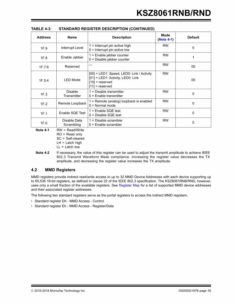
1F.9 Interrupt Level1 = Interrupt pin active high0 = Interrupt pin active low
Note 4-2 If necessary, the value of this register can be used to adjust the transmit amplitude to achieve IEEE802.3 Transmit Waveform Mask compliance. Increasing the register value decreases the TXamplitude, and decreasing the register value increases the TX amplitude.
TABLE 4-3: STANDARD REGISTER DESCRIPTION (CONTINUED)
Address Name DescriptionMode
(Note 4-1)Default
2016-2018 Microchip Technology Inc. DS00002197E-page 35
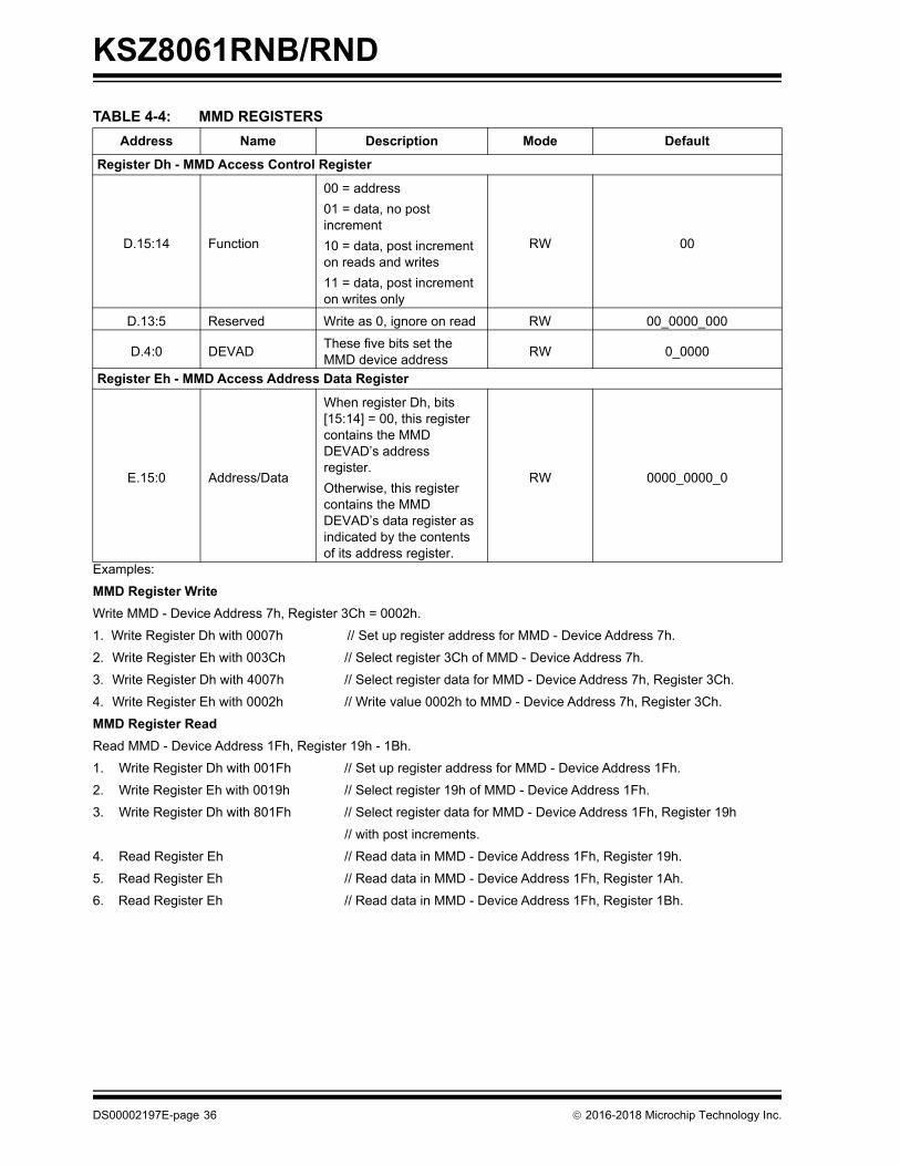
1. Write Register Dh with 001Fh // Set up register address for MMD - Device Address 1Fh.
2. Write Register Eh with 0019h // Select register 19h of MMD - Device Address 1Fh.
3. Write Register Dh with 801Fh // Select register data for MMD - Device Address 1Fh, Register 19h
// with post increments.
4. Read Register Eh // Read data in MMD - Device Address 1Fh, Register 19h.
5. Read Register Eh // Read data in MMD - Device Address 1Fh, Register 1Ah.
6. Read Register Eh // Read data in MMD - Device Address 1Fh, Register 1Bh.
TABLE 4-4: MMD REGISTERS
Address Name Description Mode Default
Register Dh - MMD Access Control Register
D.15:14 Function
00 = address
01 = data, no post increment
10 = data, post increment on reads and writes
11 = data, post increment on writes only
RW 00
D.13:5 Reserved Write as 0, ignore on read RW 00_0000_000
D.4:0 DEVADThese five bits set the MMD device address
RW 0_0000
Register Eh - MMD Access Address Data Register
E.15:0 Address/Data
When register Dh, bits [15:14] = 00, this register contains the MMD DEVAD’s address register.
Otherwise, this register contains the MMD DEVAD’s data register as indicated by the contents of its address register.
RW 0000_0000_0
DS00002197E-page 36 2016-2018 Microchip Technology Inc.
KSZ8061RNB/RND
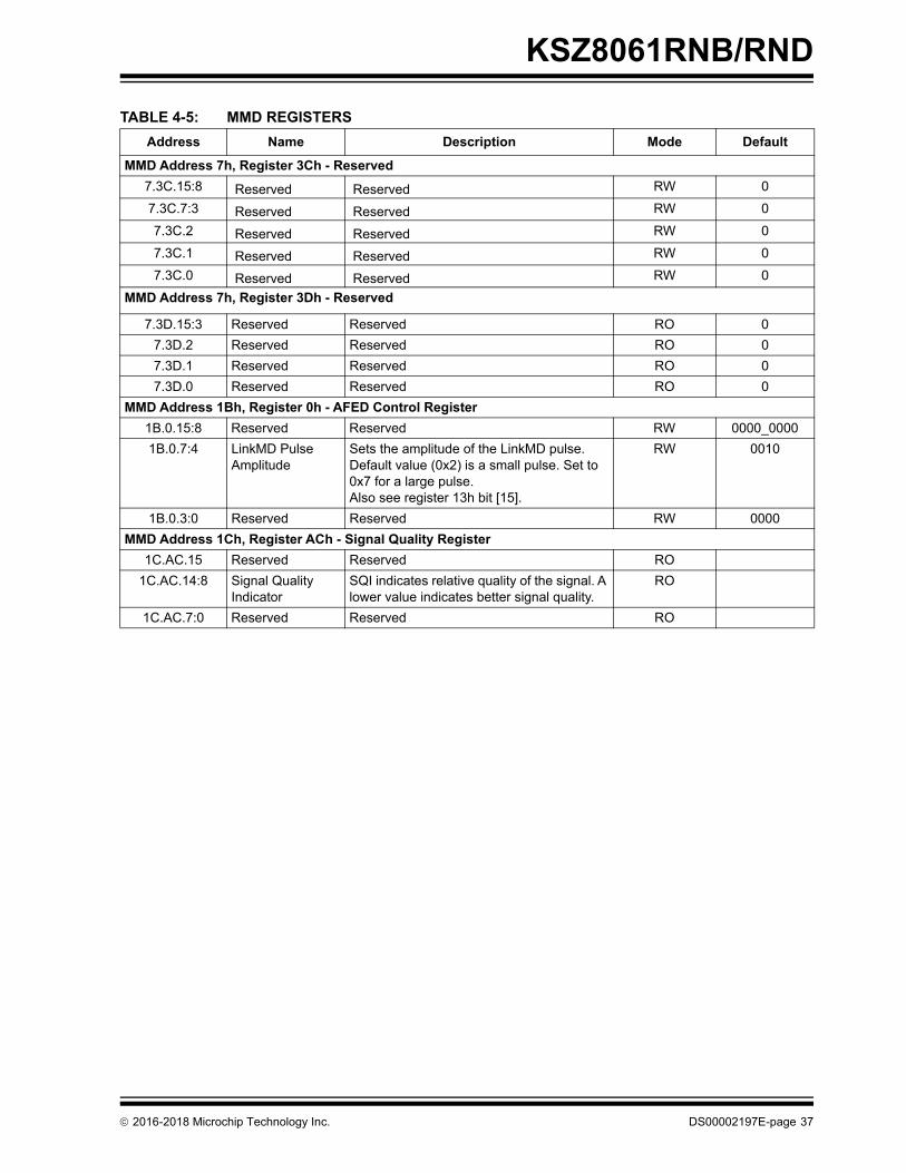
TABLE 4-5: MMD REGISTERS
Address Name Description Mode Default
MMD Address 7h, Register 3Ch - Reserved
7.3C.15:8 Reserved Reserved RW 0
7.3C.7:3 Reserved Reserved RW 0
7.3C.2 Reserved Reserved RW 0
7.3C.1 Reserved Reserved RW 0
7.3C.0 Reserved Reserved RW 0
MMD Address 7h, Register 3Dh - Reserved
7.3D.15:3 Reserved Reserved RO 0
7.3D.2 Reserved Reserved RO 0
7.3D.1 Reserved Reserved RO 0
7.3D.0 Reserved Reserved RO 0
MMD Address 1Bh, Register 0h - AFED Control Register
1B.0.15:8 Reserved Reserved RW 0000_0000
1B.0.7:4 LinkMD Pulse Amplitude
Sets the amplitude of the LinkMD pulse. Default value (0x2) is a small pulse. Set to 0x7 for a large pulse. Also see register 13h bit [15].
RW 0010
1B.0.3:0 Reserved Reserved RW 0000
MMD Address 1Ch, Register ACh - Signal Quality Register
1C.AC.15 Reserved Reserved RO
1C.AC.14:8 Signal Quality Indicator
SQI indicates relative quality of the signal. A lower value indicates better signal quality.
RO
1C.AC.7:0 Reserved Reserved RO
2016-2018 Microchip Technology Inc. DS00002197E-page 37
KSZ8061RNB/RND
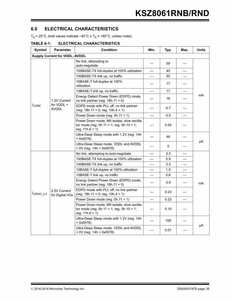
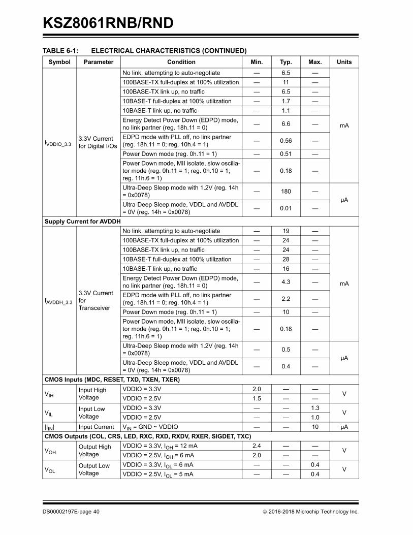
5.0 OPERATIONAL CHARACTERISTICS
5.1 Absolute Maximum Ratings*
Supply Voltage (VDDIO, AVDDH) ............................................................................................................. –0.5V to +5.0V
(VDDL, AVDDL)................................................................................................................ –0.5V to +1.8V
Input Voltage (all inputs)............................................................................................................................ –0.5V to +5.0V
Output Voltage (all inputs) ......................................................................................................................... –0.5V to +5.0V
Lead Temperature (soldering, 10sec.)...................................................................................................................+260°C
Storage Temperature (TS) ..................................................................................................................... .–55°C to +150°C
Lead Temperature Range............................................................................................Refer to JEDEC Spec. J-STD-020
* Exceeding the absolute maximum rating may damage the device. Stresses greater than the absolute maximum ratingmay cause permanent damage to the device. Operation of the device at these or any other conditions above those spec-ified in the operating sections of this specification is not implied. Maximum conditions for extended periods may affectreliability.
5.2 Operating Conditions**
Supply Voltage
(AVDDH @ 3.3V)................................................................................................................ +3.135V to +3.465V
(VDDIO @ 3.3V)................................................................................................................. +3.135V to +3.465V
(VDDIO @ 2.5V)................................................................................................................. +2.375V to +2.625V
(VDDL, AVDDL) ...................................................................................................................... +1.14V to +1.26V
Ambient Temperature
(TA, Extended) .........................................................................................................................–40°C to +105°C
Maximum Junction Temperature (TJ max) ..............................................................................................+125°C
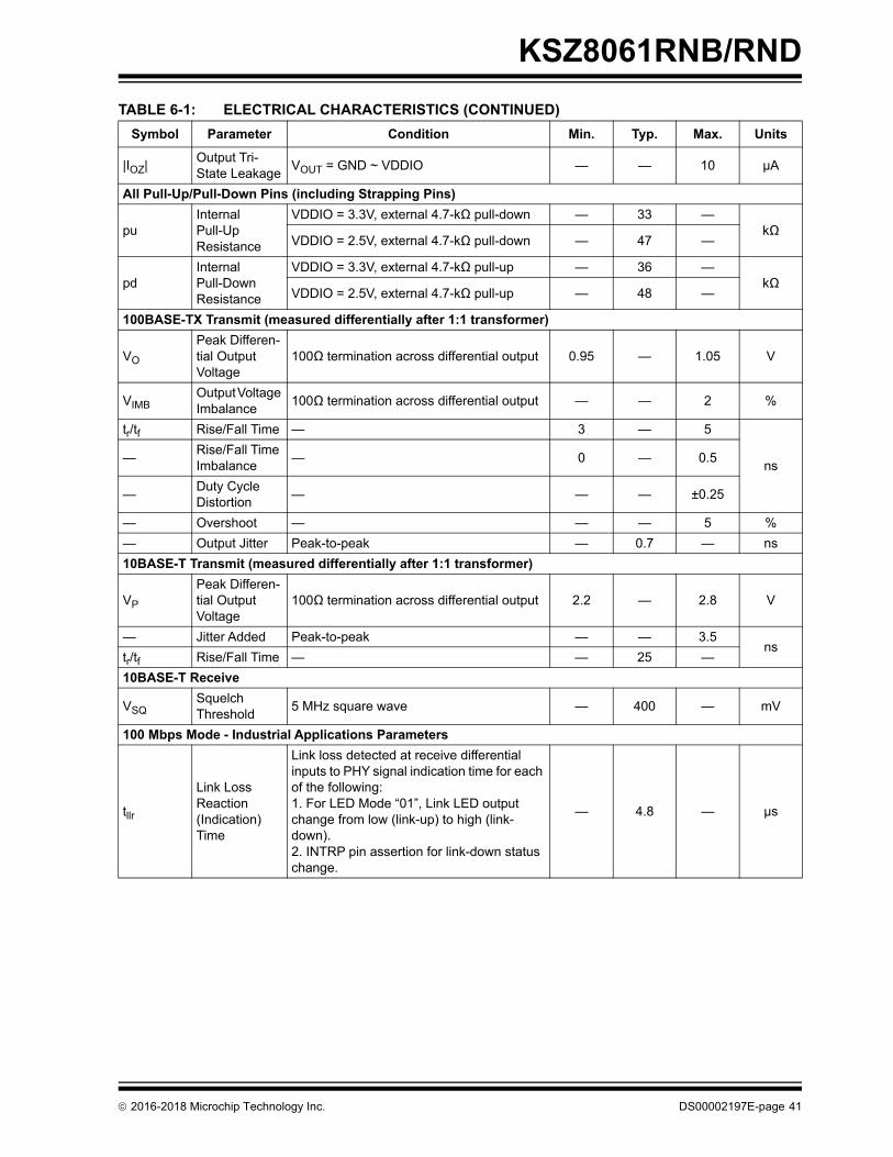
Link loss detected at receive differential inputs to PHY signal indication time for each of the following:1. For LED Mode “01”, Link LED output change from low (link-up) to high (link-down).2. INTRP pin assertion for link-down status change.
— 4.8 — µs
TABLE 6-1: ELECTRICAL CHARACTERISTICS (CONTINUED)
Symbol Parameter Condition Min. Typ. Max. Units
2016-2018 Microchip Technology Inc. DS00002197E-page 41
KSZ8061RNB/RND
7.0 TIMING DIAGRAMS
7.1 RMII Timing
FIGURE 7-1: RMII TRANSMIT TIMING
FIGURE 7-2: RMII RECEIVE TIMING
TABLE 7-1: RMII TIMING PARAMETERS
Timing Parameter
Description Min. Typ. Max. Units
tCYC Clock period — 20 —
nst1 Setup time 4 — —
t2 Hold time 2 — —
tOD Output delay 7 10 13
tCYC
REF_CLK
TXENTXD[1:0]
t1
t2
TRANSMIT TIMING
tCYC
REF_CLK
CRS_DVRXD[1:0]
RXER
tOD
RECEIVE TIMING
DS00002197E-page 42 2016-2018 Microchip Technology Inc.
KSZ8061RNB/RND
7.2 Auto-Negotiation Timing
FIGURE 7-3: AUTO-NEGOTIATION FAST LINK PULSE (FLP) TIMING
TABLE 7-2: AUTO-NEGOTIATION FAST LINK PULSE (FLP) TIMING
Timing Parameter
Description Min. Typ. Max. Units
tBTB FLP Burst to FLP Burst 8 16 24 ms
tPLPW FLP Burst width — 2 — ms
tPW Clock/Data Pulse width — 100 — ns
tCTD Clock Pulse to Data Pulse 55.5 64 69.5 µs
tCTC Clock Pulse to Clock Pulse 111 128 139 µs
— Number of Clock/Data Pulse per FLP Burst 17 — 33 —
2016-2018 Microchip Technology Inc. DS00002197E-page 43
KSZ8061RNB/RND
7.3 MDC/MDIO Timing
FIGURE 7-4: MDC/MDIO TIMING
TABLE 7-3: MDC/MDIO TIMING PARAMETERS
Timing Parameter
Description Min. Typ. Max. Units
tP MDC period 400 — —
ns
tMD1 MDIO (PHY input) setup to rising edge of MDC
10 — —
tMD2 MDIO (PHY input) hold from rising edge of MDC
4 — —
tMD3 MDIO (PHY output) delay from rising edge of MDC
5 — —
DS00002197E-page 44 2016-2018 Microchip Technology Inc.
KSZ8061RNB/RND
7.4 Power-up/Reset Timing
The KSZ8061RNB/RND reset timing requirement is summarized in Figure 7-5 and Figure 7-4.
FIGURE 7-5: POWER-UP/RESET TIMING
The supply voltage (VDDIO, AVDD, VDDL, AVDDL) power-up waveforms should be monotonic, and the 300 µs mini-mum rise time is from 10% to 90%.
For warm reset, the reset (RESET#) pin should be asserted low for a minimum of 500 µs. The strap-in pin values areread and updated at the deassertion of reset.
After the deassertion of reset, it is recommended to wait a minimum of 100 µs before starting programming on the MIIM(MDC/MDIO) Interface.
TABLE 7-4: POWER-UP/RESET TIMING PARAMETERS
Parameter Description Min. Typ. Max. Units
tvr Supply voltage (VDDIO, AVDD, VDDL, AVDDL) rise time
300 — — µs
tsr Stable supply voltage (VDDIO, AVDD, VDDL, AVDDL) to reset high
10 — — ms
tcs Configuration setup time 5 — — ns
tch Configuration hold time 5 — — ns
trc Reset to strap-in pin output 6 — — ns
SUPPLYVOLTAGES
RST#
STRAP-INVALUE
STRAP-IN /OUTPUT PIN
tVRtSR
tCS tCH
tRC
2016-2018 Microchip Technology Inc. DS00002197E-page 45
KSZ8061RNB/RND
8.0 RESET CIRCUIT
Figure 8-1 shows a reset circuit recommended for powering up the KSZ8061RNB/RND if reset is triggered by the powersupply.
FIGURE 8-1: RECOMMENDED RESET CIRCUIT
Figure 8-2 represents a reset circuit recommended for applications where reset is driven by another device (for exam-ple, CPU or FPGA). At power-on-reset, R, C, and D1 provide the necessary ramp rise time to reset the KSZ8061RNB/RND. The RST_OUT_n from CPU/FPGA provides the warm reset after power up.
FIGURE 8-2: RECOMMENDED RESET CIRCUIT FOR INTERFACING WITH CPU/FPGA RESET OUTPUT
VDDIO
D1: 1N4148
D1 R 10KΩKSZ8061RNB/KSZ8061RND
RST#
C 10μF
VDDIO
KSZ8061RNB/KSZ8061RND
D1R 10K
RST#
C 10μFD2
CPU/FPGA
RST_OUT_n
D1, D2: 1N4148
DS00002197E-page 46 2016-2018 Microchip Technology Inc.
KSZ8061RNB/RND
9.0 REFERENCE CLOCK CONNECTION AND SELECTION - KSZ8061RNB
A crystal or external clock source, such as an oscillator, is used to provide the reference clock for the KSZ8061RNB.For the KSZ8061RNB in all operating modes, the reference clock is 25 MHz. The reference clock connections to XI (pin1) and XO (pin 2), and the reference clock selection criteria are provided in Figure 9-1 and Table 9-1.
The KSZ8061RNB outputs a 50-MHz RMII reference clock on the REF_CLK pin.
2016-2018 Microchip Technology Inc. DS00002197E-page 47
KSZ8061RNB/RND
10.0 REFERENCE CLOCK CONNECTION - KSZ8061RND
The KSZ8061RND uses a 50-MHz RMII reference clock input for all of its timing. The 50-MHz clock connects to the XIpin as shown in Figure 10-1. Note that XI is powered from the AVDDH power rail, not VDDIO. The XO and REF_CLKpins are unconnected.
FIGURE 10-1: KSZ8061RND 50-MHZ CLOCK CONNECTION
NC
XI
XO
50 MHz FROMEXTERNAL
SOURCE
DS00002197E-page 48 2016-2018 Microchip Technology Inc.
KSZ8061RNB/RND
11.0 PACKAGE OUTLINES
Note: For the most current package drawings, please see the Microchip Packaging Specification located at http://www.microchip.com/packaging
FIGURE 11-1: 32-PIN 5MM × 5MM WQFN PACKAGE OUTLINE AND RECOMMENDED LAND PATTERN
2016-2018 Microchip Technology Inc. DS00002197E-page 49
All Sales listing and cover pages updated. Minor text changes throughout.
Highlights on page 1 Added this section.
Table 2-2, “Strap-in Options,” on page 8
CONFIG[2:0] 101 and 111 descriptions updated (Auto-MDI/MDI-X enabled).
Product Identification System on page 53
PIS ordering code temperature descriptions corrected. Removed note.
Table 4-1, “Standard Registers,” on page 25 and Table 4-3, “Standard Reg-ister Description,” on page 26
AFE Control 1 register information added.
Table 6-1, “Electrical Characteristics,” on page 39
Removed IVDDIO_1.8 section.
DS00002197A(08-08-16)
Whole Document Conversion of Micrel KSZ8061RNB/KSZ8061RND/KSZ8061RNB/KSZ8061RND datasheet into Microchip DS00002197E. Minor text changes throughout.
KSZ8061RNB/RND
DS00002197E-page 52 2016-2018 Microchip Technology Inc.
THE MICROCHIP WEB SITE
Microchip provides online support via our WWW site at www.microchip.com. This web site is used as a means to makefiles and information easily available to customers. Accessible by using your favorite Internet browser, the web sitecontains the following information:
• Product Support – Data sheets and errata, application notes and sample programs, design resources, user’s guides and hardware support documents, latest software releases and archived software
• General Technical Support – Frequently Asked Questions (FAQ), technical support requests, online discussion groups, Microchip consultant program member listing
• Business of Microchip – Product selector and ordering guides, latest Microchip press releases, listing of seminars and events, listings of Microchip sales offices, distributors and factory representatives
CUSTOMER CHANGE NOTIFICATION SERVICE
Microchip’s customer notification service helps keep customers current on Microchip products. Subscribers will receivee-mail notification whenever there are changes, updates, revisions or errata related to a specified product family ordevelopment tool of interest.
To register, access the Microchip web site at www.microchip.com. Under “Support”, click on “Customer Change Notifi-cation” and follow the registration instructions.
CUSTOMER SUPPORT
Users of Microchip products can receive assistance through several channels:
• Distributor or Representative
• Local Sales Office
• Field Application Engineer (FAE)
• Technical Support
Customers should contact their distributor, representative or Field Application Engineer (FAE) for support. Local salesoffices are also available to help customers. A listing of sales offices and locations is included in the back of thisdocument.
Technical support is available through the web site at: http://microchip.com/support
2016-2018 Microchip Technology Inc. DS00002197E-page 53
KSZ8061RNB/RND
NOTES:
DS00002197E-page 54 2016-2018 Microchip Technology Inc.
2016-2018 Microchip Technology Inc. DS00002197E-page 55
KSZ8061RNB/RND
Information contained in this publication regarding device applications and the like is provided only for your convenience and may besuperseded by updates. It is your responsibility to ensure that your application meets with your specifications. MICROCHIP MAKES NOREPRESENTATIONS OR WARRANTIES OF ANY KIND WHETHER EXPRESS OR IMPLIED, WRITTEN OR ORAL, STATUTORY OROTHERWISE, RELATED TO THE INFORMATION, INCLUDING BUT NOT LIMITED TO ITS CONDITION, QUALITY, PERFORMANCE,MERCHANTABILITY OR FITNESS FOR PURPOSE. Microchip disclaims all liability arising from this information and its use. Use of Micro-chip devices in life support and/or safety applications is entirely at the buyer’s risk, and the buyer agrees to defend, indemnify and holdharmless Microchip from any and all damages, claims, suits, or expenses resulting from such use. No licenses are conveyed, implicitly orotherwise, under any Microchip intellectual property rights unless otherwise stated.
Trademarks
The Microchip name and logo, the Microchip logo, AnyRate, AVR, AVR logo, AVR Freaks, BeaconThings, BitCloud, CryptoMemory, CryptoRF, dsPIC, FlashFlex, flexPWR, Heldo, JukeBlox, KEELOQ, KEELOQ logo, Kleer, LANCheck, LINK MD, maXStylus, maXTouch, MediaLB, megaAVR, MOST, MOST logo, MPLAB, OptoLyzer, PIC, picoPower, PICSTART, PIC32 logo, Prochip Designer, QTouch, RightTouch, SAM-BA, SpyNIC, SST, SST Logo, SuperFlash, tinyAVR, UNI/O, and XMEGA are registered trademarks of Microchip Technology Incorporated in the U.S.A. and other countries.
ClockWorks, The Embedded Control Solutions Company, EtherSynch, Hyper Speed Control, HyperLight Load, IntelliMOS, mTouch, Precision Edge, and Quiet-Wire are registered trademarks of Microchip Technology Incorporated in the U.S.A.
Adjacent Key Suppression, AKS, Analog-for-the-Digital Age, Any Capacitor, AnyIn, AnyOut, BodyCom, chipKIT, chipKIT logo, CodeGuard, CryptoAuthentication, CryptoCompanion, CryptoController, dsPICDEM, dsPICDEM.net, Dynamic Average Matching, DAM, ECAN, EtherGREEN, In-Circuit Serial Programming, ICSP, Inter-Chip Connectivity, JitterBlocker, KleerNet, KleerNet logo, Mindi, MiWi, motorBench, MPASM, MPF, MPLAB Certified logo, MPLIB, MPLINK, MultiTRAK, NetDetach, Omniscient Code Generation, PICDEM, PICDEM.net, PICkit, PICtail, PureSilicon, QMatrix, RightTouch logo, REAL ICE, Ripple Blocker, SAM-ICE, Serial Quad I/O, SMART-I.S., SQI, SuperSwitcher, SuperSwitcher II, Total Endurance, TSHARC, USBCheck, VariSense, ViewSpan, WiperLock, Wireless DNA, and ZENA are trademarks of Microchip Technology Incorporated in the U.S.A. and other countries.
SQTP is a service mark of Microchip Technology Incorporated in the U.S.A.
Silicon Storage Technology is a registered trademark of Microchip Technology Inc. in other countries.
GestIC is a registered trademark of Microchip Technology Germany II GmbH & Co. KG, a subsidiary of Microchip Technology Inc., in other countries.
All other trademarks mentioned herein are property of their respective companies.
Note the following details of the code protection feature on Microchip devices:
• Microchip products meet the specification contained in their particular Microchip Data Sheet.
• Microchip believes that its family of products is one of the most secure families of its kind on the market today, when used in the intended manner and under normal conditions.
• There are dishonest and possibly illegal methods used to breach the code protection feature. All of these methods, to our knowledge, require using the Microchip products in a manner outside the operating specifications contained in Microchip’s Data Sheets. Most likely, the person doing so is engaged in theft of intellectual property.
• Microchip is willing to work with the customer who is concerned about the integrity of their code.
• Neither Microchip nor any other semiconductor manufacturer can guarantee the security of their code. Code protection does not mean that we are guaranteeing the product as “unbreakable.”
Code protection is constantly evolving. We at Microchip are committed to continuously improving the code protection features of ourproducts. Attempts to break Microchip’s code protection feature may be a violation of the Digital Millennium Copyright Act. If such actsallow unauthorized access to your software or other copyrighted work, you may have a right to sue for relief under that Act.
Microchip received ISO/TS-16949:2009 certification for its worldwide headquarters, design and wafer fabrication facilities in Chandler and Tempe, Arizona; Gresham, Oregon and design centers in California and India. The Company’s quality system processes and procedures are for its PIC® MCUs and dsPIC® DSCs, KEELOQ® code hopping devices, Serial EEPROMs, microperipherals, nonvolatile memory and analog products. In addition, Microchip’s quality system for the design and manufacture of development systems is ISO 9001:2000 certified.
QUALITYMANAGEMENTSYSTEMCERTIFIEDBYDNV
== ISO/TS16949==
DS00002197E-page 56 2016-2018 Microchip Technology Inc.
AMERICASCorporate Office2355 West Chandler Blvd.Chandler, AZ 85224-6199Tel: 480-792-7200 Fax: 480-792-7277Technical Support: http://www.microchip.com/supportWeb Address: www.microchip.com
AtlantaDuluth, GA Tel: 678-957-9614 Fax: 678-957-1455
Austin, TXTel: 512-257-3370
BostonWestborough, MA Tel: 774-760-0087 Fax: 774-760-0088
ChicagoItasca, IL Tel: 630-285-0071 Fax: 630-285-0075