1328 IEEE JOURNAL OF SOLID-STATE CIRCUITS, VOL. 42, NO. 6, JUNE 2007
A CDMA Dual-Band Zero-IF ReceiverWith Integrated LNAs and VCOs in an
Advanced SiGe BiCMOS ProcessDavid Simmonds, Member, IEEE, Raymond T. Cheung, Taoling Fu, Peter Borowitz, Richard Schwab,
Robert Ruth, Per Karlsen, and Klaas van Zalinge, Member, IEEE
Abstract—This paper describes one of the first dual PCS- andCEL-band CDMA receivers that includes LNAs and VCOs ona single die. The PCS-band LNA achieves a noise figure (NF) of1.5 dB and IP3 of+7.5 dBm at 16-dB gain. The PCS demodulatingmixer achieves an NF of 5 dB, IP3 of +5 dBm and uncalibratedIP2 of+60 dBm. The PCS VCO is capable of 134 dBc/Hz phasenoise at 3.9 GHz and 1.25-MHz offset. A copper BiCMOS processwas chosen for both performance and cost benefits, comparedwith lower geometry CMOS.
Index Terms—CDMA, direct conversion, low-noise amplifiers(LNAs), receivers, voltage-controlled oscillators (VCOs).
I. INTRODUCTION
THERE is a clear trend towards CMOS for RFICs due tocost benefits of reduced digital block size and the desire
for single-chip integration [1]–[3]. However, most RFIC de-signers in industry, if given a choice between BiCMOS andCMOS, would choose BiCMOS due to better RF performanceand design flexibility. Although the performance gap betweenBiCMOS and CMOS RF is shrinking, the reduced voltage ca-pability of thin-oxide CMOS devices makes circuit design morechallenging and can give increased current consumption wherefolding becomes necessary.
This paper describes a high-performance CDMA receiver ICdesigned to be compatible with both legacy and future basebandASICs, where the legacy analog-to-digital converters (ADCs)are only 6 b. This means that the analog baseband chain musthave a wide dynamic range and circuit blocks are consequentlyphysically large. Advanced CMOS processes m arepresently expensive per square millimeter of die area and alsoin nonreturnable expenditure (NRE). In this application, thelarge ratio of analog-to-digital block area means that 0.25- mBiCMOS is cheaper than the 0.12- m CMOS, which would
Manuscript received September 10, 2006; revised January 10, 2007.D. Simmonds was with Nokia, San Diego, CA 92131 USA. He is now with
Musicians Institute, Hollywood, CA 90028 USA (e-mail: [email protected]).
R. T. Cheung was with Nokia, San Diego, CA 92131 USA. He is now withGeneral Atomics, San Diego, CA 92121 USA.
T. Fu, R. Schwab, and P. Karlsen were with Nokia, San Diego, CA 92131USA. They are now with ST Microelectronics, San Diego, CA 92121 USA.
P. Borowitz was with ST Microelectronics, San Diego, CA 92121 USA.R. Ruth was with Nokia, San Diego, CA 92131 USA. He is now retired.K. van Zalinge was with Nokia, San Diego, CA 92131 USA. He is now with
Qualcomm Inc., San Diego, CA 92121 USA.Digital Object Identifier 10.1109/JSSC.2007.897154
TABLE IMINIMUM AND TARGET SYSTEM PERFORMANCE
have been required for similar performance. IC process choiceand system partitioning are strongly interdependent and requirea thorough evaluation at the start of a project.
II. SYSTEM REQUIREMENTS
Minimum CDMA system requirements are given in ANSI/TIA/EIA-98-D [4] and are summarized in Table I. Target designspecifications at room temperature were generally 3 dB tougherthan those given by EIA-98-D, to give competitive advantageand customer satisfaction.
Designing a receiver for the CDMA standard is more awk-ward than designing one for GSM or WCDMA, due to specifi-cations related to single-tone desensitization (STD) [5], [6] andtwo-tone blocking. STD can be system-partitioned into blockspecifications for LNA IP3 and VCO phase noise. In this case,the LNA IIP3 requirement was 7 dBm and VCO phasenoise 128 dBc/Hz at 900-kHz offset from a 3.5-GHz carrierin the CEL band. Two-tone blocking is specified by phone-car-rier compliance testing and in this IC leads to requirement onmixer IP2 to be 55 dBm.
SIMMONDS et al.: CDMA DUAL-BAND ZERO-IF RECEIVER WITH INTEGRATED LNAs AND VCOs IN AN ADVANCED SiGe BICMOS PROCESS 1329
Challenging system requirements, together with toughmarket forces, help explain why there are relatively few CDMAchipset providers.
III. DUAL-BAND RECEIVER CONFIGURATION
LNAs for CDMA CEL and PCS bands have three gain stepsto optimize dynamic range and coincide with EIA-98-D inter-modulation testing at three input levels. A fixed-gain GPS LNAis also included, for use with a GPS module. CDMA LNA out-puts connect to an off-chip dual-band SAW filter that attenuatesTX signals and provides single-ended-to-balanced conversionfor input to demodulating mixers. Outputs of the two mixersare connected together via MOS switches and then to basebandamplifier input. The baseband amplifier has unity DC gain andselectable 15- or 9-dB gain with a 400-Hz high-pass charac-teristic set by two external capacitors. The unity-gain low-passfilter provides 615-kHz CDMA bandwidth definition and 65-dBattenuation at 900 kHz by means of a seventh-order elliptic re-sponse. A variable gain amplifier (VGA) provides up to 72-dBgain in 3-dB steps with DC compensation and a 400-Hz high-pass response set with two external capacitors. An output 7-bDAC provides compensation for static DC offsets in 2.5-mVsteps.
The LO is synthesized by an integer-N-type phase-lockedloop (PLL) and includes calibration circuitry for the VCOtuning. The VCO contains two cores, optimized for each band,that operate at 3.5 and 3.9 GHz to reduce leakage in the RXband and allow digital LO dividers for IQ phase accuracy.Power is supplied direct from the battery via on-chip lowdrop-out voltage regulators (LDOs), and one of these has verylow noise for use with VCO. Voltage regulators take 3.1–5.4-Vinput and produce an output of 2.7 V for block use. The chipis controlled by a three-wire serial bus and serial input–output(SIO) logic is distributed into three blocks to reduce bussinglayout area, with some lines gated to reduce interference.
A common bias block provides various output currents forall analog blocks, except for the VCO, which needed very lownoise bias. An external trimmed 1.35-V reference was availablefrom the baseband ASIC, so this was used instead of an internalbandgap to reduce bias variation and layout area. Accurate con-stants with temperature currents were made with 1.35-V refer-ence and an external 1% 27 k resistor by op-amp and mirrorconfiguration. PTAT currents were generated, with a delta VBEcircuit and an external 1% 2k7 resistor, to generate a 25- Aunit current. The bias block also generates some currents pro-portional to internal resistor types, so that process variation iscancelled to first order, for example, in LO voltage swing andbaseband IQ output DC offset DACs.
Most blocks have two separate bias registers, each with twocontrol bits, to allow for current versus performance optimiza-tion and fast switching between “Normal” and “Economy”mode bias settings. Mode switching between Normal andEconomy modes is dependent on gain setting and mode controlbits are located in the gain control register to minimize DSPoverhead. Normal-mode current consumption is 70 mA andEconomy-mode consumption is 55 mA.
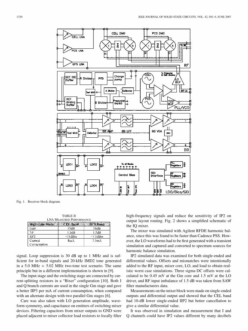
The die size is 10.9 mm and the die is packaged in an 81-ball5 5 mm BGA. The BGA package was chosen for lower cost
and higher pin count, compared with QFN. Fig. 1 shows thereceiver block diagram.
IV. BLOCK DESIGN AND MEASUREMENTS
A. LNAs
The three-gain CDMA LNA topology used here is verysimilar to that well described in [6] and was optimized for ICprocess change from BiCMOS6G to BiCMOS7RF. Three npntransistors with different degeneration are connected at theircollectors to provide gain switching, and a low-frequency inputtrap improves IIP3.
Maximum current was increased to allow higher IIP3, andthe process change meant that the PCS band could now be in-tegrated. PCS LNA gain was increased by double bonding theemitter with 90 bond wires connected to adjacent edges of thepackage to reduce mutual inductance.
A package model for LNA package pins and BGA substratewas extracted by EM simulation with Ansoft Q3D software.LNA simulations were done with Agilent RFDE Harmonic Bal-ance, which allows native support of distributed, frequency-dis-persive, printed wiring board (PWB) line features.
Table II summarizes CDMA LNA performance in high gainmode for both bands.
B. Mixers
The previous generation to this IC used an IP2 tuning schemedescribed in [6] and this had some weakness with temperaturesensitivity and LO leakage from DC offset LO waveforms.
After much simulation and test chip investigation of differenttopologies, it became clear that the basic Gilbert Mixer IIP2could not be tuned or made sufficiently good with precise layoutand that an alternative approach was required. Differential IIP2depends on both single-ended output IIP2 and balance cancel-lation. It may be supposed that very good layout matching of1% could give 40-dB cancellation of IMD2 products; however,simulation showed that, with worst case RF, LO, and device mis-matches, the Intermod products themselves were unbalanced inboth amplitude and phase by greater than 1-dB amplitude and10 phase, so that significantly less cancellation is realizable.This means that it is necessary to reduce or filter the IMD2product before it appears at the output.
The main contribution to IP2 occurs at the Gm input stagedue to second-order intermodulation-generating low-frequencyIMD2 products, not in the switching mixer stage or due to self-mixing [7], [8]. In general, input stage nonlinearity generatescommon-mode IMD2 products and LO switching asymmetrygenerates differential-mode IMD2 products.
The two generic ways to prevent IMD2 products reaching theoutput are by feedback or high-pass filtering. Filtering by ACcoupling the Gm stage to switching stage is very effective, pro-vided high-impedance current sources are used to prevent IMD2voltages appearing as currents, but gives increased current con-sumption and noise.
This design reduces IMD2 products by a common-modefeedback loop around the Gm stage bias and functions becauseIMD2 tone at this point is predominantly a common-mode
1330 IEEE JOURNAL OF SOLID-STATE CIRCUITS, VOL. 42, NO. 6, JUNE 2007
Fig. 1. Receiver block diagram.
TABLE IILNA MEASURED PERFORMANCE
signal. Loop suppression is 30 dB up to 1 MHz and is suf-ficient for in-band signals and 20-kHz IMD2 tone generatedin a 5.0 MHz 5.02 MHz two-tone test scenario. The sameprinciple but in a different implementation is shown in [9].
The input stage and the switching stage are connected by cur-rent-splitting resistors in a “Bixer” configuration [10]. Both Iand Q branch currents are used in the single Gm stage and gavea better IIP3 per mA of current consumption, when comparedwith an alternate design with two parallel Gm stages [6].
Care was also taken with LO generation amplitude, wave-form symmetry, and capacitance on emitters of switching mixerdevices. Filtering capacitors from mixer outputs to GND wereplaced adjacent to mixer collector load resistors to locally filter
high-frequency signals and reduce the sensitivity of IP2 onoutput layout routing. Fig. 2 shows a simplified schematic ofthe IQ mixer.
The mixer was simulated with Agilent RFDE harmonic bal-ance, since this was found to be faster than Cadence PSS. How-ever, the LO waveforms had to be first generated with a transientsimulation and captured and converted to spectrum sources forharmonic balance simulation.
IP2 simulated data was examined for both single-ended anddifferential values. Offsets and mismatches were intentionallyadded to the RF input, mixer core, LO, and load to obtain real-istic worst case simulations. Three sigma DC offsets were cal-culated to be 0.45 mV at the Gm core and 1.5 mV at the LOdriver, and RF input imbalance of 1.5 dB was taken from SAWfilter manufacturers data.
Measurements on the mixer block were made on single-endedoutputs and differential output and showed that the CEL bandhad 10-dB lower single-ended IIP2 but better cancellation togive a similar differential value.
It was observed in simulation and measurement that I andQ channels could have IP2 values different by many decibels
SIMMONDS et al.: CDMA DUAL-BAND ZERO-IF RECEIVER WITH INTEGRATED LNAs AND VCOs IN AN ADVANCED SiGe BICMOS PROCESS 1331
Fig. 2. Mixer schematic.
TABLE IIIDEMODULATING MIXER MEASURED PERFORMANCE
and that system performance really depends on the sum of in-terfering energies, so that an “ ” IIP2 metric is a goodperformance representation, as shown in
IIPIIP IIP
(1)
This effectively relaxes IIP2 specification in cases where onechannel is close to limit, but other channel IIP2 is much higher.Table III summarizes the measured mixer performance for bothbands.
C. Baseband
The baseband amplifier provides low-noise 0–18-dB gain in3-dB steps, although optimized phone AGC just uses 15- and9-dB settings. The amplifier has unity DC gain, and the high-pass corner is set to 400 Hz by two external 1- F capacitors;these capacitors have a high value because the impedance level
is made low for noise reasons. The supply current of the base-band amplifier was set to minimize the degradation of the RXchain values for IIP3 and IIP2 when compared with raw demod-ulating mixer performance.
To meet the requirements of 65-dB attenuation at 900 kHzand 0.5-dB attenuation at 615 kHz, a seventh-order ellipticfilter with a Chebychev passband is used, with one notch fallingclose to 900 kHz. The filter has 5-b tuning with switched re-sistors to cover the worst case process. A calibration tone of640 kHz is generated from 19.2-MHz crystal input frequency
1332 IEEE JOURNAL OF SOLID-STATE CIRCUITS, VOL. 42, NO. 6, JUNE 2007
Fig. 4. VGA block diagram.
by a divide-by-30 circuit and a DSP algorithm sets the level ofthe calibration tone to be between 3 and 6 dB down comparedwith a wide tuned response. To reduce temperature variation ofthe corner frequency, two types of poly resistors with oppositetemperature coefficients were scaled to give first-order cancel-lation, and this reduced corner frequency variation to approxi-mately 5 kHz. Resistor temperature coefficients were found tobe dependent on exact resistor geometry and a little differentfrom design kit values, so some empirical optimization of theresistor ratio was required.
Fig. 3 shows a plot of the temperature-compensated passbandresponse for three devices, measured with the whole RX chainat 30, 25, and 85 c.
The baseband VGA provides up to 72-dB gain in 3-dB stepsand consists of three main stages where VGA1 has 0-, 15-, and30-dB steps, VGA2 has 0-, 6-, 9-, and 12-dB steps, and Outputstage has 0-, 15-, and 30-dB steps. Miller compensation capaci-tors are switched in value as gain is switched to maintain op-ampphase margins. DC compensation is provided with aid of twoexternal 220-nF capacitors which set the high-pass corner to bebelow 400 Hz. DC offset is sensed at the capacitor nodes byadditional op-amps and subtracted from the input response, toimprove DC rejection by over 40 dB. The VGA was designedto handle a maximum 20-mV input DC offset and, with a worstcase gain step, this gives a 640-mV peak output offset and a5-ms settling time. However, measured worst case input offsetwas approximately 5 mV and a software controlled switch isused to speed up capacitor charge/discharge at gain step where
offset voltage step is worst case, so measured settling times wereless than 1 ms.
A low value of the high-pass corner was found to be necessaryfor good additive white Gaussian noise (AWGN) performance inmeasurements and systems simulation, even though a fractionalCDMA bandwidth calculation would suggest a few KHz shouldbe sufficient.
A 7-b DAC is connected to feedback resistors of VGA outputstage and provides static DC compensation in 2.5-mV steps.Phone software runs a compensation algorithm periodically totune DAC and so corrects errors over temperature and in Base-band ASIC input.
Fig. 4 shows a VGA block diagram.A wideband peak level detector is connected to demodulating
mixer output and was originally intended to detect strong inter-fering signal and swap the baseband amplifier and VGA gainsby 6 dB to improve linearity. However, it was also beneficial inthe AGC to set conditional LNA gain modes and improve lin-earity in a two-tone test.
Table IV summarizes mixer input to baseband output chainmeasured performance for both bands.
D. VCOs
Optimum Inductor choice is crucial to good VCO design,with consideration to Q, tuning range, and impedance levelwith respect to active devices. The inductance of 1 nH inthe CEL band and 1.1 nH in PCS was chosen to maximizethe voltage swing to 4 V peak-to-peak differential, without
SIMMONDS et al.: CDMA DUAL-BAND ZERO-IF RECEIVER WITH INTEGRATED LNAs AND VCOs IN AN ADVANCED SiGe BICMOS PROCESS 1333
TABLE IVMIXER TO BASEBAND CHAIN MEASURED PERFORMANCE
saturating the oscillator core or exceeding reliability limits andto give a roughly equal noise contribution as the core-collectorcurrent shot noise. The inductor width of 40 m was chosento optimize Q at an operating frequency to 25, without addingtoo much parasitic capacitance. The inductors were availableas standard parameterized cells in Design Kit library and areconstructed with thick Copper octagonal metallization andgrounded patterned polysilicon shield.
Phase noise is very dependent on Kvco and RF voltage acrossVaractors, but it is also necessary to guarantee a tuning rangeover IC process corners, and this means that switched tuningis required. A MathCAD sheet was used to calculate Varactor,MIM, and switched capacitance from required tuning range anddesired Varactor/MIM voltage ratio.
Total tank Q is the reciprocal sum of individual componentQ’s, so the Q of each component must be optimized, and greatcare is needed with layout component placements and intercon-nect traces to minimize additional routing resistance.
Several small MIM capacitors are used in parallel, to increasecapacitor Q to around 200 and to get around IC process restric-tions on the number of vias per capacitor. The Varactor was a PNjunction type, rather than a MOS type, and the finger width wassized as a compromise between Q and parasitic capacitance.
Three pairs of switched capacitors are binary weighted to giveeight tuning steps. nMOS switch devices use 0.25 m minimumgate length and widths are binary scaled. Absolute nMOS sizesare a compromise between ON-resistance and parasitic capaci-tance (tuning range). MOS switches connect capacitors directly,rather than via GND, and logic inverters provide gate–sourceoverdrive voltage to ensure that switches are maximally ON orOFF [11].
If a positive frequency versus tune voltage is desired, then theVaractor needs a method for GND bias, and this is awkward in adifferential circuit. Some papers have shown resistive bias, butthis adds noise and degrades tank Q [12]. The alternative, as wasdone here, was to inductively choke the RF with two low-areainductors. Choke inductance was optimally set at ten times thetank inductance, and the width was scaled for best overall tankQ. The Varactor GND return tracking was separated and takento the star point at the VCO GND bond pad to prevent VCOblock noise from modulating the varactor. The choke inductorsadd layout area and some parasitic capacitance but provide a netimprovement in phase noise.
Total tank Q is around 18 at mid tuning and degrades slightlywhen all MOS switches are turned ON. Equivalent series resis-tance of the tank is about 1.3 , and this low value emphasizes
the need for great layout care. The VCO layout was also de-signed to ensure that there were no parasitic metal loops aroundinductor, for example in guard bands, since these would act asa magnetic shorted turn and severely degrade Q.
The VCO core features a common mode feedback loop whichdecreases low-frequency impedance at tail, helps to set optimumbias point, modifies current pulse shape and improves phasenoise around 2 dB.
The core’s nMOS current source was scaled with a relativelysmall ratio to minimize 4 KT noise and an RF de-coupling capacitor was placed on its drain. It should be notedthat using a large ratio will give large Gm and large noise,which can then be inductively filtered as in [13]. The 1-pF ca-pacitor on current source drain reduces RF swing at this node,shapes current pulses, and was found to improve phase noisearound 2 dB.
Although there have been some papers published with verygood phase-noise CMOS core oscillators [14], this designerfound that best performance at 4 GHz was achievable, in thisIC process, with a bipolar core due to lower transistor noise.However, the bipolar core suffers from a potential problemover process and temperature, where increasing current givestransistor saturation, causing phase noise to degrade drastically.To prevent saturation and set the optimum operating point, anautomatic level control (ALC) is used [12]. An ALC feedbackloop detects tank voltage and controls current through theoscillator core. Level detection is done by a differential peakdetector does, where voltage on capacitor is a rectified andsmoothed version of input waveform [15].
To reduce noise, the peak detector is embedded in an oper-ational transconductance amplifier (OTA) and resistors replacecurrent sources. The input AC level is tapped down by a capac-itive divider to prevent reverse-biasing detector transistors oninput peaks. DC reference of OTA comes direct from the VCObandgap, and the DC-bias-to-AC-detector leg is a selectable re-sistively scaled version of bandgap voltage. NPN devices andbias resistors are matched so that ALC-controlled tank voltageis approximately process-independent [16].
A capacitor to GND on the gate of the current source sets thedominant pole of the ALC loop and filters noise from the ALC.
It should be noted that, although Leeson’s equation has pro-portionality to Q squared, in an ALC voltage-limited system,doubling Q only gives a 3-dB, not a 6-dB, noise benefit becausecurrent is halved to maintain same voltage swing.
Fig. 5 shows the VCO core and ALC simplified schematic.A bandgap reference operating at 0.5 mA provides two low-
noise reference voltages needed by the ALC, and this is basedon Brokaw topology [17]. The Brokaw topology has reasonablenoise performance because NPN devices are resistively degen-erated; also, it is not susceptible to base current errors and gen-erates both Vbe and within the same two-transistor cell.
The VCO bias block also provides IC process-compensatedbias currents to buffer blocks, so that de-generation voltages areconstant, and this avoids risk of up-converted bias noise fromoverdriven buffers. Bias currents of buffers can be halved foreconomy mode savings.
Cadence SpectreRF was used for VCO simulation andits PNOISE analysis includes linear additive noise, mixing
1334 IEEE JOURNAL OF SOLID-STATE CIRCUITS, VOL. 42, NO. 6, JUNE 2007
Fig. 5. VCO core and ALC schematic.
Fig. 6. Measured PCS-band phase noise.
multiplicative noise, and nonlinear time-variant mechanisms.Cadence PNOISE summary was used to examine the top-per-centage noise contributors and optimize design. Linear ACanalysis and calculator functions for bandwidth and imagi-nary/real definitions of Q were used to optimize tank Q.
Fig. 6 shows PCS band noise to be 134 dBc/Hz at 1.25-MHzoffset and 3.9 GHz. The VCO core current was about 6 mA andgives a phase-noise figure of merit (FOM) for the CEL band of
189 and 192 for the PCS band, which compares well to the bestpublished values [14]. Phase noise is about 3 dB better than thatreported for a similar CDMA CMOS VCO, allowing for centerfrequency [1]. In fact, the phase noise was sufficiently withinspecifications that the ALC setting could be reduced and currentsaved.
VCO performance with a PLL is summarized for both bandsin Table V.
SIMMONDS et al.: CDMA DUAL-BAND ZERO-IF RECEIVER WITH INTEGRATED LNAs AND VCOs IN AN ADVANCED SiGe BICMOS PROCESS 1335
TABLE VVCO WITH PLL MEASURED PERFORMANCE
E. PLL
The settling time requirement for a CDMA PLL is 2.5 ms,which is relatively slow compared with GSM, and this meansthat an integer-N PLL with 3-kHz bandwidth is adequate.In-band phase noise (1–615 kHz) sets the ultimate RX signalto noise obtainable, and 24 dBc at an LO frequency wasdeemed to be adequate for evolution-data-optimized (EV-DO)application. It should be noted that tougher in-band phase noisewould have required a fractional-N PLL.
Although there have been several papers promoting a phase-switching-type prescaler, it can have problems with waveformasymmetry causing subharmonic reference spurs on the VCOspectrum [18]. In this design, a conventional 64/65 prescalerwith a synchronous 4/5 bipolar core was used and was optimizedfor current consumption with the aid of an internal DC feedbackloop to give constant voltage swings. It should be noted thatthe 4/5 divider core has four potential outputs, each separatedby 90 , but only one of these will give the minimum clock-to-modulus control delay when connected to A and B counters; thisissue can cause a PLL to fail at certain channels but is rarelymentioned in the literature.
Counters for R, A, and B dividers, as shown in Fig. 1, weredesigned to be pseudosynchronous with resynchronization tominimize current consumption and accumulated phase noise.The duty cycle was also made low to reduce high-frequencyenergy for spur reduction reasons.
The VCO design required a low Kvco for phase-noise rea-sons and, to guarantee tuning range over worst case processand conditions, a high-voltage charge-pump was required. Thecharge-pump was designed with high-voltage bipolar devices,incorporated beta compensation, and provided 10% mismatchwithin 0.5–4.1-V output range. The reference spur level wasbelow 55 dBc.
Charge-pump current is 1.0 mA in the CEL band and 1.33 mAin the PCS band to compensate for differences in N and give thesame loop bandwidth in both bands; Kvco is same for CEL andPCS VCOs.
The PLL includes calibration circuitry to set VCO 3-b tuningat each requested channel change. In this scheme, the loop filteris precharged to the middle voltage of frequency versus Vtunecharacteristic and tuning CAL bits are set to mid values. A phasecomparator measures if the main divider output is high or low
with respect to the reference divider, and a successive approx-imation register (SAR) halves the CAL bit count at each com-parison frequency interval to find the correct 3-b CAL code infour reference frequency periods. After calibration, the loop isclosed and the PLL locks quickly since the tune voltage is ef-fectively precharged. Requirements for this scheme are that thereference divider, main divider, and PFD must be reset and thatVCO tuning curves must overlap.
V. TOP-LEVEL VERIFICATION AND IC TESTABILITY
The IC was verified to be functionally correct from SIO pro-gramming to the baseband output at the top level, in externalLO mode, using HSIM transient simulation. Digital logic wasrepresented at full transistor level, but simulator accuracy wasset more loosely for those blocks. RF signals were applied afterprogramming and DC stabilization to optimize simulation time,and useful data were obtainable overnight. Cadence Spectre DCand transient analysis was also used at the top level, but withvoltage source representation of internal logic lines. With thesesimulation tools, it was possible to catch two previously unseenpower-up and oscillation problems before GDSII tapeout.
A mass-production IC needs to be thoroughly testable forboth performance at the development stage and for manufac-turing defects at the production stage. Testability needs to bedesigned in at the start to avoid costly redesign, and, in this case,the following features were included; pin access to mixer out-puts and baseband inputs, baseband chain multiplex switching,PLL divider test output, external LO input, LDO Kelvin access,VCO test buffer output, and IC version number readable via se-rial input–output interface. Test features were also verified bysimulation to be functionally correct.
Total device cost can be partitioned approximately equallybetween die size, package, and testing, so that it is necessary tominimize test time while still providing adequate test coverage.Adding test pins, test modes, read-back registers, and designingout calibrations speeds up test time and eases the bench test.
VI. BICMOS7RF PROCESS
This IC was fabricated on STMicroelectronics’ BiCMOS7RFprocess, which contains many state-of-the-art performance fea-tures. Very low noise, 60-GHz Ft carbon-doped SiGe NPN tran-sistors are available, which benefited every block, particularlyLNAs, VCOs, and mixers, and enabled integration of the PCS-band LNA. High-voltage (5-V) variants of this device were alsoused, for example, in the PLL charge-pump.
Digital library with 0.25- m geometry CMOS enabledshrinking of digital control blocks and PLL dividers from pre-vious-generation ICs described in [6]. A 0.35- m low-leakagedigital library was also available and used in analog blocks.
Top-layer 4- m-thick Copper with 5-m /sq resistivity wasused for inductors, RF, and supply routing. This layer had afactor of 10 less resistivity than the M2–M4 layers and allowschoices of high Q or low-area inductors and low resistance orthinner routing.
High-Q MIM capacitors at the M4–M5 levels provide5-fF/ m density and are stackable above other devices, as inthe LPF.
1336 IEEE JOURNAL OF SOLID-STATE CIRCUITS, VOL. 42, NO. 6, JUNE 2007
Fig. 7. Phone sensitivity with and without prescaler spurs.
Deep trench isolation (DTI) was used at both the device levelfor reduced capacitance and at the block level for isolation. LOleakage is critical in direct conversion, and DTI helped makeleakage 20 dB better than specifications. It was also crucial inreducing system problems, as described in Section VII.
VII. SYSTEM INTERFERENCE ISSUES AND ESD
The first version of this IC had a problem where PLLout-of-band phase noise could increase up to 6 dB, dependingon CDMA input and gain levels, due to coupling from basebandblocks to VCO. To fix this, a DTI/GND/DTI sandwich wasplaced around the VCO, with GND taken to a dedicated pin.There was a cut in isolating GND to prevent a metal ring, givinga shorted turn degradation of the VCO inductor Q. With thissecond full-mask iteration, measured phase-noise degradationbecame less than 0.2 dB over the whole CDMA dynamic range.
Another system-type problem was found later after an all-channel sensitivity sweep, where spurs generated by the PLLprescaler fell into the CEL RF band and desensitized the receiverby up to 2.0 dB. Spurs were synchronous with modulus con-trol signal and generated 120-kHz comb at the CEL band whichgave, depending on the RF channel number, 30- or 60-kHz base-band spurs, with every fourth channel clean. RF spurs werepicked up in the LNA and mixer, but the VCO spectrum wasclean. To fix this problem, several steps were taken; a second iso-lating buffer was added to the prescaler input, substrate couplingwas reduced with a DTI/GND/DTI sandwich added around thePLL with continuous GND to short the magnetic field, big fil-tering capacitors (BFCs) and 10- series resistors were addedto analog and digital prescaler supplies to make high-frequencycurrent circulate locally rather than through bond wires. Withthis third full-mask iteration, the spur level measured at the base-band output was reduced 15 dB, and no receiver desensitiza-tion was measurable in phone. Fig. 7 shows measured sensitivityplots for three phones with B-version ICs and then remeasuredwith final C-version ICs.
The first version of this IC was found to have some ESDweakness, and it became apparent that device voltage limits forthe more modern IC process had decreased but ESD pad designand choice had not kept track. Voltage transients on each pad
TABLE VIMEASURED SYSTEM PERFORMANCE
Fig. 8. Die microphotograph.
type were simulated with a representation of the human bodymodel (HBM), and then all unique current paths were analyzedto determine the total voltage that would be seen by a deviceconnected to pad; these voltages were then compared with de-vice maximum ratings. To reduce ESD transient voltages, moreclamps were added around the ring to reduce IR drops, addi-tional series resistance was added to some MOS gate connec-tions, and some pads were changed with a number of posi-tive supply diodes set as the best compromise between ESDperformance and false power-up/leakage scenarios. After thesechanges, a 1-kV HBM rating was obtainable.
VIII. CONCLUSION
This paper describes one of the first mass production dualCEL–PCS-band CDMA receiver ICs with integrated LNAs and
SIMMONDS et al.: CDMA DUAL-BAND ZERO-IF RECEIVER WITH INTEGRATED LNAs AND VCOs IN AN ADVANCED SiGe BICMOS PROCESS 1337
VCOs. Previously published CDMA receivers have been eitherCEL-band only or required an external LO signal.
The IC uses circuit topology enhancements for mixer, VCO,and VGA blocks and utilizes the advantages of an advancedBiCMOS process to meet tough performance requirements.
The measured system performance is summarized in Table VIand shows good margin to EIA-98-D.
System interference problems, which are a risk with increasedintegration levels, were found and were overcome with layoutfeatures and circuit changes.
ESD problems, which are a risk with IC-process feature-sizereduction, were found and were overcome with pad and circuitchanges.
Also, supply current reduction, through the use of “Normal”and “Economy” modes, have contributed to an outstandingphone standby time of 13 days.
Fig. 8 shows a microphotograph of the die in a wafer.
ACKNOWLEDGMENT
The authors would like to thank C. Wakeham, Y. Rasse,and J.-C. Grasset for realizing the JDC and its management,E. Reynaud, D. Banh, and J. Mjelde for layout efforts, andL. Pan and J. Kiraly for project support. The authors would liketo acknowledge Q. Gu for RF system design and support andH. Toscano and R. Chen for ATE development and measure-ments. This IC was designed as part of a Joint DevelopmentCentre (JDC) between Nokia and ST Microelectronics inSan Diego, and some blocks were made by specialized teamsin Grenoble. Thanks also to ST Microelectronics in Grenoblefor fabrication, test and project support.
REFERENCES
[1] V. Aparin, K. NamSoo, G. Brown, W. Yue, A. Cicalini, S. Kwok,and C. Persico, “A fully-integrated highly linear zero-IF CMOS cel-lular CDMA receiver,” in IEEE ISSCC Dig. Tech. Papers, 2005, pp.324–325.
[2] G. Gramegna, P. G. Mattos, M. Losi, S. Das, M. Franciotta, N. G. Bel-lantone, M. Vaiana, V. Mandara, and M. Paparo, “A 56-mW 23-mmsq single-chip 180-nm CMOS GPS receiver with 27.2-mW 4.1-mm sqradio,” IEEE J. Solid-State Circuits, vol. 41, no. 3, pp. 540–551, Mar.2006.
[3] Y. H. Hsieh, W. Y. Hu, S. M. Lin, C. L. Chen, W. K. Li, S. J. Chen,and D. J. Chen, “An auto-I/Q calibrated CMOS transceiver for 802.11g,” IEEE J. Solid-State Circuits, vol. 40, no. 11, pp. 2187–2192, Nov.2005.
[4] Recommended Minimum Performance Standards for CDMA 2000Spread Spectrum Mobile Stations, ANSI/TIA/EIA-98-D Standard,Jun. 2001.
[5] B. Ko, D. Cheon, S. Kim, J. Ko, J. Kim, and B. Park, “A nightmare forCDMA RF receiver: The cross modulation,” in Proc. 1st Asia-PacificConf. ASICS, Seoul, Korea, Aug. 1999, pp. 400–402.
[6] M. Hafizi, S. Feng, T. Fu, K. Schulze, R. Ruth, R. Schwab, P. Karlsen,D. Simmonds, and Q. Gu, “RF front-end of direct conversion receiverRFIC for CDMA-2000,” IEEE J. Solid-State Circuits, vol. 39, no. 10,pp. 1622–1632, Oct. 2004.
[7] D. Manstretta, M. Brandolini, and F. Svelto, “Second-order intermod-ulation mechanisms in CMOS downconverters,” IEEE J. Solid-StateCircuits, vol. 38, no. 3, pp. 394–406, Mar. 2003.
[8] D. Coffing and E. Main, “Effects of offsets on bipolar integrated circuitmixer even-order distortion terms,” IEEE Trans. Microw. Theory Tech.,vol. 49, no. 1, pp. 23–30, Jan. 2001.
[9] M. W. Hwang, S. Y. Yoo, J. C. Lee, J. Lee, and G. H. Cho, “A High IIP2direct-conversion mixer using an even harmonic reduction techniquefor cellular CDMA/PCS/GPS applications,” in IEEE RFIC Symp. Dig.,Jun. 2004, pp. 39–42.
[10] H. Waite, P. Ta, J. Chen, H. Li, M. Gao, C. S. Chang, W.Redman-White, O. Charlon, Y. Fan, R. Perkins, D. Brunel, E.Soudee, N. Lecacheur, and S. Clamagirand, “A CDMA 2000 zero-IFreceiver with low-leakage integrated front end,” IEEE J. Solid-StateCircuits, vol. 39, no. 7, pp. 1175–1179, Jul. 2004.
[11] H. Sjoland, “Improved switched tuning of differential CMOS VCOs,”IEEE Trans. Circuits Syst. II, Analog Digit. Signal Process., vol. 49,no. 5, pp. 352–355, May 2002.
[12] A. Zanchi, C. Samori, S. Levantino, and A. L. Lacaita, “A 2-V 2.5-GHz-104-dBc/Hz at 100 kHz fully integrated VCO with wideband low-noise automatic amplitude control loop,” IEEE J. Solid-State Circuits,vol. 36, no. 4, pp. 611–619, Apr. 2001.
[13] P. Andreani and H. Sjoland, “Tail current noise suppression in RFCMOS VCOs,” IEEE J. Solid-State Circuits, vol. 37, no. 3, pp.342–348, Mar. 2002.
[14] E. Hegazi, H. Sjoland, and A. A. Abidi, “A filtering technique to lowerLC oscillator phase noise,” IEEE J. Solid-State Circuits, vol. 36, no.12, pp. 1921–1930, Dec. 2001.
[15] R. G. Meyer, “Low-power monolithic RF peak detector analysis,” IEEEJ. Solid-State Circuits, vol. 30, no. 1, pp. 65–67, Jan. 1995.
[16] M. A. Margarit, J. L Tham, R. G. Meyer, and M. J. Deen, “A low-noise, low-power VCO with automatic amplitude control for wirelessapplications,” IEEE J. Solid-State Circuits, vol. 34, no. 6, pp. 761–771,Jun. 1999.
[17] A. P. Brokaw, “A simple three-terminal IC bandgap reference,” IEEEJ. Solid-State Circuits, vol. SSC-9, no. 12, pp. 388–393, Dec. 1974.
[18] J. Craninckx and M. S. J. Steyaert, “A 1.75-GHz/3-V dual-modulusdivide-by-128/129 prescaler in 0.7- �m CMOS,” IEEE J. Solid-StateCircuits, vol. 31, no. 7, pp. 890–897, Jul. 1996.
David Simmonds (M’02) was born in Bristol, U.K.,in 1965. He received the B.Sc. (Hons.) degree inphysics from Imperial College, London University,London, U.K., in 1986.
From 1986 to 1992, he was with The BritishBroadcasting Corporation, initially as a RadioEngineer with the Broadcasting House and then asa Radio Frequency Designer with the Design andEquipment Department. In 1992, he joined Nokia,San Diego, CA, where he was involved with mobilephone RF design for the first four years and RFIC
design until 2006. His last position with Nokia included VCO and top-leveldesign of a highly integrated CDMA receiver IC. He is now with the MusiciansInstitute, Hollywood, CA.
Raymond T. Cheung received the Higher Diplomain electronic engineering from the Hong KongPolytechnic, Hong Kong, in 1987, the B.S. degree inelectrical engineering from Polytechnic University,Brooklyn, NY, in 1997, and the M.S. degree inelectrical engineering from Virginia PolytechnicUniversity, Blacksburg, in 1998.
He joined Nokia, San Diego, CA, in 1999, wherehe was involved with RF circuit design for CDMAhandsets. He is currently with General Atomics, SanDiego, CA.
Taoling Fu received the B.Eng. (Hons.) degree inelectronic engineering from Hong Kong Polytechnic,Hong Kong, in 1991, and the M.S.E.E. degree fromNortheastern University, Boston, MA, in 1995.
He joined Nokia Mobile Phones, San Diego, CA,in 1995 as an RF Engineer and subsequently joinedthe RFIC Design Group in 2000. He is currently withST Microelectronics, San Diego, as an RFIC DesignEngineer with the Advanced Radio ArchitectureGroup.
1338 IEEE JOURNAL OF SOLID-STATE CIRCUITS, VOL. 42, NO. 6, JUNE 2007
Peter Borowitz, photograph and biography not available at the time ofpublication.
Richard Schwab received the B.S.E.E. degree fromSan Diego State University, San Diego, CA, in 1994.
He was with Triquint Semiconductor in GaAs PAdesign before joining the IC Design Group, NokiaMobile Phones, San Diego, CA, in 1998. He is cur-rently with STMicroelectronics, San Diego.
Robert Ruth received the B.S.E.E. degree from SanDiego State University, San Diego, CA, in 1973.
He has designed memories and mixed-signalICs using both CMOS and bipolar technology.Between 1994 and 2005, he was with Nokia MobilePhones, San Diego, CA, where he was involvedwith developing CDMA receiver designs in bothsuper-heterodyne and direction-conversion architec-tures. He is now retired.
Per Karlsen received the M.S.E.E. degree from theTechnical University of Denmark, Copenhagen, in1994.
In 1994, he became a Research Engineer withthe Center for Broadband Telecommunications,Technical University of Denmark, where he wasinvolved with developing GaAs front-end ICs foroptical communications. From 1995 to 2006, he wasinvolved with GSM and CDMA chipset develop-ment with Nokia Mobile Phones in Copenhagen andSan Diego, CA. Since 2006, he has been with the
Advanced Radio Architecture Group, STMicroelectronics, San Diego.
Klaas van Zalinge (M’93) was born in Amsterdam,The Netherlands, in 1956. He received the M.Sc. de-gree in electrical engineering from Delft Universityof Technology, Delft, The Netherlands, in 1983.
From 1992 to December 1997, he was withSTMicroelectronics, France, where he was involvedwith analog IC design for consumer products. InJanuary 1998, he joined Nokia, San Diego, CA,where he was involved with analog circuits forCDMA transmitters and receivers. Since November2006, he has been with Qualcomm Inc., San Diego,
working on RF CMOS designs for cellular applications. His research interestsare in RF analog CMOS circuits and systems for wireless communications.