apm6668 Wi-Fi 802.11 b/g/n & Dual mode BLE Dual Radio Module Pre-Production Information Data Sheet ` Page 1 of 35 apm Communication, Inc. – TEL: 886-3-666-1188 – FAX: 886-3-666-8033 Website: http://www.apmcomm.com – E-mail: [email protected]apmcomm Proprietary and Confidential – Product information is subject to change without notice.–Jul. 9.2015 apm6668 Wi-Fi 802.11 b/g/n & Dual Mode BLE Dual Radio Module DESCRIPTION With a small form factor of 9×11×1.55mm max., the apm6668 is a full-featured WiFi 802.11b/g/n & Dual mode Bluetooth low energy Dual mode module that simultaneously provides WiFi and Bluetooth connections. By providing flexible host interfaces combined with support for embedded operating systems, the apm6668 enables rapid integration of WiFi and Bluetooth technology into a variety of host devices. The pre-tested and pre-certified module eliminates the need to create custom designs, resulting in greatly reduced development risk, costs, and time-to-market. GENERAL FEATURES Small footprint: 9×11×1.55 mm max Support for state-of-the-art WiFi-Bluetooth co-existence and VoIP optimizations Support for single antenna configuration for WiFi and Bluetooth EEPROM and full RF front-end integrated for WiFi and Bluetooth External clock sharing for WiFi and Bluetooth Excellent GSM/GPRS/DCS/PCS/WCDMA/GPS radio coexistence Support for drivers on embedded OS RoHS compliant WIFI FEATURES IEEE 802.11b/g/n compliant Host interface: SDIO 1-bit, SDIO 4-bit, SDIO SPI Support for WAPI security Supports Access Point tethering functionality (Soft AP for Linux and Android ) Designed for Wi-Fi Direct™ Hardware encryption support for WEP40/64, WEP104/128, TKIP, CCMP (AES) and BIP provides functionality for WPA, WPA2, IEEE 802.11i, IEEE 802.11w BLUETOOTH FEATURES Dual-mode Bluetooth®/Bluetooth low energy radio Fully qualifiable Bluetooth v4.0 IC Can be used as part of a Bluetooth v4.0 + HS system High-speed UART port (up to 4Mbps) APPLICATIONS Smart phone / PDA / PDA phone / WiFi phone / DSC / DVC with both WiFi and Bluetooth connectivity APPEARANCE
Transcript
apm6668 Wi-Fi 802.11 b/g/n & Dual mode BLE Dual Radio Module Pre-Production Information Data Sheet
` Page 1 of 35 apm Communication, Inc. – TEL: 886-3-666-1188 – FAX: 886-3-666-8033 Website: http://www.apmcomm.com – E-mail: [email protected] apmcomm Proprietary and Confidential – Product information is subject to change without notice.–Jul. 9.2015
apm6668 Wi-Fi 802.11 b/g/n & Dual Mode BLE Dual Radio Module DESCRIPTION
With a small form factor of 9×11×1.55mm max.,
the apm6668 is a full-featured WiFi 802.11b/g/n & Dual
mode Bluetooth low energy Dual mode module that
simultaneously provides WiFi and Bluetooth
connections.
By providing flexible host interfaces combined
with support for embedded operating systems, the
apm6668 enables rapid integration of WiFi and
Bluetooth technology into a variety of host devices. The
pre-tested and pre-certified module eliminates the need
to create custom designs, resulting in greatly reduced
development risk, costs, and time-to-market.
GENERAL FEATURES
Small footprint: 9×11×1.55 mm max
Support for state-of-the-art WiFi-Bluetooth
co-existence and VoIP optimizations
Support for single antenna configuration for WiFi and
Bluetooth
EEPROM and full RF front-end integrated for WiFi
and Bluetooth
External clock sharing for WiFi and Bluetooth
Excellent GSM/GPRS/DCS/PCS/WCDMA/GPS
radio coexistence
Support for drivers on embedded OS
RoHS compliant
WIFI FEATURES
IEEE 802.11b/g/n compliant
Host interface: SDIO 1-bit, SDIO 4-bit, SDIO SPI
Support for WAPI security
Supports Access Point tethering functionality
(Soft AP for Linux and Android ) Designed for Wi-Fi Direct™
Hardware encryption support for WEP40/64,
WEP104/128, TKIP, CCMP (AES) and BIP
provides functionality for WPA, WPA2, IEEE
802.11i, IEEE 802.11w
BLUETOOTH FEATURES
Dual-mode Bluetooth®/Bluetooth low energy radio
Fully qualifiable Bluetooth v4.0 IC
Can be used as part of a Bluetooth v4.0 + HS system
High-speed UART port (up to 4Mbps)
APPLICATIONS
Smart phone / PDA / PDA phone / WiFi phone / DSC
/ DVC with both WiFi and Bluetooth connectivity
APPEARANCE
apm6668 Wi-Fi 802.11 b/g/n & Dual mode BLE Dual Radio Module Pre-Production Information Data Sheet
` Page 2 of 35 apm Communication, Inc. – TEL: 886-3-666-1188 – FAX: 886-3-666-8033 Website: http://www.apmcomm.com – E-mail: [email protected] apmcomm Proprietary and Confidential – Product information is subject to change without notice.–Jul. 9.2015
REVISION HISTORY
Date Release Author Description 2014.10.14 0.1 Ryan Initial release
2015.05.19 0.2 Ryan Changed BT transmit power
2015.07.09 1.0 Ryan
Updated the Product appearance & Modify
Pre-condition test condition 168 hrs &
add IEEE Specification RX sensitivity(6Mbps,
54Mbps,MCS7)
apm6668 Wi-Fi 802.11 b/g/n & Dual mode BLE Dual Radio Module Pre-Production Information Data Sheet
` Page 3 of 35 apm Communication, Inc. – TEL: 886-3-666-1188 – FAX: 886-3-666-8033 Website: http://www.apmcomm.com – E-mail: [email protected] apmcomm Proprietary and Confidential – Product information is subject to change without notice.–Jul. 9.2015
1-1 GENERAL SPECIFICATION....................................................................................................................................... 5
1-3-4 PIO Pins........................................................................................................................................................ 12
1-3-6 Power Pins .................................................................................................................................................... 13
1-4 BLUETOOTH PINS .................................................................................................................................................. 13
1-4-4 PIO Pins........................................................................................................................................................ 15
1-4-5 Power Pins .................................................................................................................................................... 15
1-5 EXTERNAL VOLTAGE SOURCE .............................................................................................................................. 15
1-5-2 Bluetooth Reset ............................................................................................................................................. 16
1-6-1 Absolute Maximum Rating........................................................................................................................... 19
1-7 CURRENT CONSUMPTION ..................................................................................................................................... 20
1-7-1 WLAN Current Consumption....................................................................................................................... 20
1-7-2 Bluetooth Current Consumption.................................................................................................................. 21
apm6668 Wi-Fi 802.11 b/g/n & Dual mode BLE Dual Radio Module Pre-Production Information Data Sheet
` Page 4 of 35 apm Communication, Inc. – TEL: 886-3-666-1188 – FAX: 886-3-666-8033 Website: http://www.apmcomm.com – E-mail: [email protected] apmcomm Proprietary and Confidential – Product information is subject to change without notice.–Jul. 9.2015
1-8-2 Bluetooth RF Specification .......................................................................................................................... 24
2-1-1 OS Support & Available Drivers................................................................................................................... 30
2-1-2 Security Features Supported ........................................................................................................................ 30
2-1-3 Other Features .............................................................................................................................................. 30
2-2 BLUETOOTH SOFTWARE STACKS.......................................................................................................................... 31
4-1 RECOMMENDED MOUNTING PAD DESIGN (TOP VIEW) ....................................................................................... 33
4-2 RECOMMENDATION FOR STENCIL APERTURE IN SMT PROCESS ........................................................................ 33
4-3 BAKING CONDITION RECOMMENDATION BEFORE IR REFLOW............................................................................ 35
4-4 RECOMMENDATION FOR REFLOW PROFILE ........................................................................................................ 35
apm6668 Wi-Fi 802.11 b/g/n & Dual mode BLE Dual Radio Module Pre-Production Information Data Sheet
` Page 5 of 35 apm Communication, Inc. – TEL: 886-3-666-1188 – FAX: 886-3-666-8033 Website: http://www.apmcomm.com – E-mail: [email protected] apmcomm Proprietary and Confidential – Product information is subject to change without notice.–Jul. 9.2015
Antenna External single antenna support. The output impedance is 50Ω.
apm6668 Wi-Fi 802.11 b/g/n & Dual mode BLE Dual Radio Module Pre-Production Information Data Sheet
` Page 6 of 35 apm Communication, Inc. – TEL: 886-3-666-1188 – FAX: 886-3-666-8033 Website: http://www.apmcomm.com – E-mail: [email protected] apmcomm Proprietary and Confidential – Product information is subject to change without notice.–Jul. 9.2015
1-1-1 Block Diagram
PIO
EEPROM
Matching
PIO
SDIO/SDIO SPI
HCI (UART)& audio PCM interface
Coexistence
BPF Debug SPI
Debug SPI
Bluetooth SOC
(ROM HCI Firmware)
Clock
FEM WiFi SOC
1.8V3.3V
Circuit
apm6668 Wi-Fi 802.11 b/g/n & Dual mode BLE Dual Radio Module Pre-Production Information Data Sheet
` Page 7 of 35 apm Communication, Inc. – TEL: 886-3-666-1188 – FAX: 886-3-666-8033 Website: http://www.apmcomm.com – E-mail: [email protected] apmcomm Proprietary and Confidential – Product information is subject to change without notice.–Jul. 9.2015
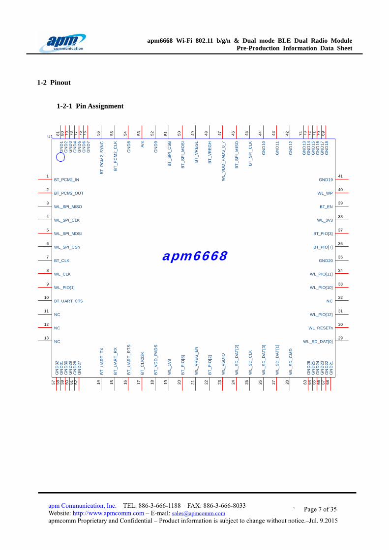
1-2 Pinout
1-2-1 Pin Assignment
apm6656
U1
WL_3V338
WL_SPI_CSn6
WL_
SD
_DA
T[1
]27
BT_CLK7
BT_PIO[3]37
GND2035
BT
_VD
D_P
AD
S18
WL_PIO[11]34
BT_EN39
GND1941
WL_SPI_CLK4
GN
D10
44
WL_
SD
_CLK
25
BT_V
RE
GH
48
BT_PCM2_OUT2
BT
_CLK
32K
17
WL_SPI_MISO3
NC32
WL_
1V8
19
WL_WP40
WL_SPI_MOSI5
BT
_PIO
[8]
20
BT
_UA
RT
_RX
15
BT
_PIO
[2]
22
GN
D11
43
BT_PCM2_IN1
BT_
SPI
_CS
B51
BT
_UA
RT
_TX
14
GN
D9
52
WL_SD_DAT[0]29
WL_
VDD
_PAD
S_0_
747
WL_
VSD
IO23
WL_
SD
_DA
T[2
]24
WL_CLK8
WL_RESETn30
BT_S
PI_
MIS
O46
Ant
53
WL_
VR
EG
_EN
21
NC12
BT
_UA
RT
_RT
S16
BT_UART_CTS10
NC11
BT
_PC
M2_
CLK
55
BT_PIO[7]36
NC13
WL_
SD
_CM
D28
BT_V
RE
GL
49
BT
_SP
I_C
LK45
GN
D8
54
BT_S
PI_
MO
SI
50
BT_P
CM
2_SY
NC
56
WL_PIO[1]9
WL_
SD
_DA
T[3
]26
WL_PIO[12]31
WL_PIO[10]33
GN
D12
42
GN
D32
57
GN
D31
58
GN
D30
59
GN
D29
60
GN
D28
61
GN
D27
62
GN
D26
63
GN
D25
64
GN
D24
65
GN
D23
66
GN
D18
69G
ND
1770
GN
D16
71G
ND
1572
GN
D14
73
GN
D22
67
GN
D21
68
GN
D13
74
GN
D7
75G
ND
676
GN
D5
77G
ND
478
GN
D3
79G
ND
280
GN
D1
81
apm6668
apm6668 Wi-Fi 802.11 b/g/n & Dual mode BLE Dual Radio Module Pre-Production Information Data Sheet
` Page 8 of 35 apm Communication, Inc. – TEL: 886-3-666-1188 – FAX: 886-3-666-8033 Website: http://www.apmcomm.com – E-mail: [email protected] apmcomm Proprietary and Confidential – Product information is subject to change without notice.–Jul. 9.2015
1-2-2 Pin Description
* I/O: Digital Input/Output, I: Digital Input, O: Digital Output, A: Analog, PU: Pull-up, PD: Pull-down
# Name I/O Pin Status on Reset Supply Domain Description
1 BT_PCM2_IN I PD BT_VDD_PADS Synchronous data input
2 BT_PCM2_OUT O PD BT_VDD_PADS Synchronous data output
3 WL_SPI_MISO O PD WL_VDD_PADS_0_7 Debug SPI data output
4 WL_SPI_CLK I PD WL_VDD_PADS_0_7 Debug SPI clock
5 WL_SPI_MOSI I PD WL_VDD_PADS_0_7 Debug SPI data input
6 WL_SPI_CSn I PU WL_VDD_PADS_0_7 Debug SPI chip select, active low
23 WL_VSDIO Power - - Positive supply for SDIO interface
24 WL_SD_DAT[2] I/O PU WL_VSDIO SDIO bidirectional data line (not used in CSPI mode)
25 WL_SD_CLK I PU WL_VSDIO SDIO or CSPI clock line
26 WL_SD_DAT[3] I/O PU WL_VSDIO SDIO bidirectional data line or CSPI chip select
apm6668 Wi-Fi 802.11 b/g/n & Dual mode BLE Dual Radio Module Pre-Production Information Data Sheet
` Page 9 of 35 apm Communication, Inc. – TEL: 886-3-666-1188 – FAX: 886-3-666-8033 Website: http://www.apmcomm.com – E-mail: [email protected] apmcomm Proprietary and Confidential – Product information is subject to change without notice.–Jul. 9.2015
# Name I/O Pin Status on Reset Supply Domain Description
27 WL_SD_DAT[1] I/O PU WL_VSDIO SDIO bidirectional data line or CSPI interrupt
28 WL_SD_CMD I PU WL_VSDIO SDIO bidirectional command line or CSPI MOSI
29 WL_SD_DAT[0] I/O PU WL_VSDIO SDIO bidirectional data line or CSPI MISO
38 WL_3V3 Power - - Positive supply for AIO[0]-AIO[3] , PIO[8]-PIO[15], and FEM
39 BT_EN I - BT_VDD_PADS Chip enable
40 WL_WP I - - Write protection for internal EEPROM
41 GND GND - - Ground
42 GND GND - - Ground
43 GND GND - - Ground
44 GND GND - - Ground
45 BT_SPI_CLK I PD BT_VDD_PADS SPI clock
46 BT_SPI_MISO O PD BT_VDD_PADS SPI data output
47 WL_VDD_PADS_0_7 Power - - Positive supply for Debug SPI, PIO[0]-PIO[7]
48 BT_VREGH Power - - High regulator input
49 BT_VREGL Power - - High regulator output and low regulator input
50 BT_SPI_MOSI I PD BT_VDD_PADS SPI data input
51 BT_SPI_CSB I PD BT_VDD_PADS Chip select for Serial Peripheral Interface, active low
52 GND GND - - Ground
53 ANT A - - RF input/output
54 GND GND - - Ground
55 BT_PCM2_CLK I/O PD BT_VDD_PADS Synchronous data clock
apm6668 Wi-Fi 802.11 b/g/n & Dual mode BLE Dual Radio Module Pre-Production Information Data Sheet
` Page 10 of 35 apm Communication, Inc. – TEL: 886-3-666-1188 – FAX: 886-3-666-8033 Website: http://www.apmcomm.com – E-mail: [email protected] apmcomm Proprietary and Confidential – Product information is subject to change without notice.–Jul. 9.2015
# Name I/O Pin Status on Reset Supply Domain Description
56 BT_PCM2_SYNC I/O PD BT_VDD_PADS Synchronous data sync
All the big pads on the bottom of the module should be tied to ground.
apm6668 Wi-Fi 802.11 b/g/n & Dual mode BLE Dual Radio Module Pre-Production Information Data Sheet
` Page 11 of 35 apm Communication, Inc. – TEL: 886-3-666-1188 – FAX: 886-3-666-8033 Website: http://www.apmcomm.com – E-mail: [email protected] apmcomm Proprietary and Confidential – Product information is subject to change without notice.–Jul. 9.2015
1-3 WiFi Pins
1-3-1 SDIO Pins
apm6668 supports a SDIO device interface that conforms to the industry standard SDIO Full-Speed card
specification and allows a host controller using the SDIO bus protocol to access apm6668.
The SDIO bus has weak internal pull up resistors on chip.
SDIO Bus Name Pin # Pin Name SD 1-bit Mode SD 4-bit Mode
DAT3 26 WL_SD_DAT[3] SD :Card detect DAT[3]/CD :Data line 1 or card detect
DAT2 24 WL_SD_DAT[2] RW: Read wait DAT[2]/RW :Data line 1 or read wait
DAT1 27 WL_SD_DAT[1] IRQ#: Interrupt DAT[1]/IRQ# :Data line 1 or interrupt
DAT0 29 WL_SD_DAT[0] DATA: Data line DAT[0]: Data line 0
CMD 28 WL_SD_CMD CMD: Command line CMD: Command line
CLK 25 WL_SD_CLK CLK: Clock CLK: Clock
1-3-2 CSPI Pins
While SDIO port is not available on host platform, apm6668 supports a SD-SPI device interface that connects to
Synchronous Serial Port (SSP) pins.
The SD-SPI bus has weak internal pull up resistors on chip.
SD-SPI Name Pin # Pin Name Description
CS 26 WL_SD_DAT[3] Card Select
IRQ 27 WL_SD_DAT[1] Interrupt
DO 29 WL_SD_DAT[0] MISO:Data output
DI 28 WL_SD_CMD MOSI:Data input
SCLK 25 WL_SD_CLK Clock
apm6668 Wi-Fi 802.11 b/g/n & Dual mode BLE Dual Radio Module Pre-Production Information Data Sheet
` Page 12 of 35 apm Communication, Inc. – TEL: 886-3-666-1188 – FAX: 886-3-666-8033 Website: http://www.apmcomm.com – E-mail: [email protected] apmcomm Proprietary and Confidential – Product information is subject to change without notice.–Jul. 9.2015
1-3-3 Debug SPI Pins
apm6668 has a SPI interface for test and debugging purposes. The lab tools, such as UniTest and UniPSUtil, can
communicate with apm6668 WiFi part using the SPI protocol over a connection to an LPT port.
Debug SPI Name Pin # Pin Name Description
MISO 3 WL_SPI_MISO Debug SPI data output
MOSI 5 WL_SPI_MOSI Debug SPI data input
CLK 4 WL_SPI_CLK Debug SPI clock
CSn 6 WL_SPI_CSn Debug SPI chip select, active low
VDDIO 47 WL_VDD_PADS_0_7 Serial I/O VDD
1-3-4 PIO Pins
The PIO pins are used to implement user defined input and output signals to and from the module such as external
interrupts, LED controlled outputs, and other user-defined I/Os. Each PIO can be independently controlled.
WL_PIO[1]: WiFi External clock request out Other PIOs: Reserved
1-3-5 WP Pin
WL_WP is write protection for internal EEPROM. The internal EEPROM stores calibration table, MAC address,
etc. for WiFi part. When the pin is pulled high, it protects the EEPROM content. If tied to VSS, normal memory
read/write operation is enabled.
The WiFi firmware does not incorporate any support for writing to the EEPROM during normal operation. This
significantly reduces the risk of spurious writes corrupting the contents of the EEPROM, and means it is not possible
to repair any damage that may occur. Hence, it is suggested that keep the pin, WL_WP, permanently pulled high to
minimize the risk of data corruption.
apm6668 Wi-Fi 802.11 b/g/n & Dual mode BLE Dual Radio Module Pre-Production Information Data Sheet
` Page 13 of 35 apm Communication, Inc. – TEL: 886-3-666-1188 – FAX: 886-3-666-8033 Website: http://www.apmcomm.com – E-mail: [email protected] apmcomm Proprietary and Confidential – Product information is subject to change without notice.–Jul. 9.2015
1-3-6 Power Pins
The following list shows the pins referenced to WL_VSDIO.
Pin # Pin name Pin # Pin name Pin # Pin name
24 WL_SD_DAT[2] 25 WL_SD_CLK 26 WL_SD_DAT[3]
27 WL_SD_DAT[1] 28 WL_SD_CMD 29 WL_SD_DAT[0]
The following list shows the pins referenced to WL_VDD_PADS_0_7.
Pin # Pin name Pin # Pin name Pin # Pin name
3 WL_SPI_MISO 4 WL_SPI_CLK 5 WL_SPI_MOSI
6 WL_SPI_CSn 30 WL_RESETn
The following list shows the pins referenced to WL_3V3.
Pin # Pin name Pin # Pin name Pin # Pin name
9 WL_PIO[1] 33 WL_PIO[10] 34 WL_PIO[11]
31 WL_PIO[12]
*WL_VDD_PADS_0_7 voltage power level must be the same as BT_VDD_PADS and the oscillator.
1-4 Bluetooth Pins
1-4-1 UART Pins
apm6668 supports a Universal Asynchronous Receiver Transmitter (UART) interface with programmable baud
rate up to 4Mbps. BlueCore Serial Protocol (BCSP), a proprietary alternative to the standard Bluetooth UART Host
Transport, is also supported.
UART Bus Name Pin # Pin Name Description
CTS 10 BT_UART_CTS UART clear to send active low
RTS 16 BT_UART_RTS UART request to send active low
TX 14 BT_UART_TX UART data output active high
RX 15 BT_UART_RX UART data input active high
VDDIO 18 BT_VDD_PADS Serial I/O VDD
apm6668 Wi-Fi 802.11 b/g/n & Dual mode BLE Dual Radio Module Pre-Production Information Data Sheet
` Page 14 of 35 apm Communication, Inc. – TEL: 886-3-666-1188 – FAX: 886-3-666-8033 Website: http://www.apmcomm.com – E-mail: [email protected] apmcomm Proprietary and Confidential – Product information is subject to change without notice.–Jul. 9.2015
1-4-2 PCM Pins
apm6668 audio Pulse Code Modulation (PCM) interface supports continuous transmission and reception of PCM
encoded audio data over Bluetooth. The Digital Audio Interface (I2S) shares the same pins as the PCM interface.
Bus Name Pin # Pin Name Description
SYNC 56 BT_PCM2_SYNC PCM: PCM2 Synchronous data sync I2S: I2S_WS
CLK 55 BT_PCM2_CLK PCM: PCM2 Synchronous data clock I2S: I2S_SCK
OUT 2 BT_PCM2_OUT PCM: PCM2 Synchronous data output I2S: I2S_OUT
IN 1 BT_PCM2_IN PCM: PCM2 Synchronous data input I2S: I2S_IN
VDDIO 18 BT_VDD_PADS Serial I/O VDD
PCM2/I2S interface mapping
1-4-3 Debug SPI Pins
apm6668 has a SPI interface for debug primarily. The lab tools, PSTOOL, can communicate with apm6668 BT
part using the SPI protocol over a connection to an LPT port.
Debug SPI Name Pin # Pin Name Description
MISO 46 BT_SPI_MISO Debug SPI data output
MOSI 50 BT_SPI_MOSI Debug SPI data input
CLK 45 BT_SPI_CLK Debug SPI clock
CS 51 BT_SPI_CSB Debug SPI chip select, active low
VDDIO 18 BT_VDD_PADS Serial I/O VDD
apm6668 Wi-Fi 802.11 b/g/n & Dual mode BLE Dual Radio Module Pre-Production Information Data Sheet
` Page 15 of 35 apm Communication, Inc. – TEL: 886-3-666-1188 – FAX: 886-3-666-8033 Website: http://www.apmcomm.com – E-mail: [email protected] apmcomm Proprietary and Confidential – Product information is subject to change without notice.–Jul. 9.2015
1-4-4 PIO Pins
The PIO pins are used to implement user defined input and output signals to and from the module such as external
interrupts, LED controlled output and other user-defined I/Os. Each PIO can be independently controlled.
BT_PIO[7]: LED Bluetooth TX activities. BT_PIO[2]: Bluetooth external clock request out.
BT_PIO[3]: Bluetooth external clock request in.
BT_PIO[8]: LED Bluetooth RX activities.
1-4-5 Power Pins
The following list shows the pins referenced to BT_VDD_PADS.
Pin # Pin name Pin # Pin name Pin # Pin name
1 BT_PCM2_IN 22 BT_PIO[2] 55 BT_PCM2_CLK
2 BT_PCM2_OUT 36 BT_PIO[7] 56 BT_PCM2_SYNC
10 BT_UART_CTS 37 BT_PIO[3]
14 BT_UART_TX 39 BT_EN
15 BT_UART_RX 45 BT_SPI_CLK
16 BT_UART_RTS 46 BT_SPI_MISO
17 BT_CLK32K 50 BT_SPI_MOSI
20 BT_PIO[8] 51 BT_SPI_CSB
*BT_VDD_PADS voltage power level must be the same as WL_VDD_PADS_0_7
1-5 External Voltage Source
The external supply rails to apm6668 should have less than 10mV rms noise levels between 0 to 10 MHz. Single
tone frequencies are also to be avoided.
Transient response of external regulators used should be <= 5us for WiFi and <= 20us for Bluetooth, respectively.
Supply voltage range
1.8V 1.8V+/- 5% (ripple Vpp<10mV rms)
3.3V 3.3V +/-5% (ripple Vpp<10mV rms)
apm6668 Wi-Fi 802.11 b/g/n & Dual mode BLE Dual Radio Module Pre-Production Information Data Sheet
` Page 16 of 35 apm Communication, Inc. – TEL: 886-3-666-1188 – FAX: 886-3-666-8033 Website: http://www.apmcomm.com – E-mail: [email protected] apmcomm Proprietary and Confidential – Product information is subject to change without notice.–Jul. 9.2015
1-5-1 WiFi Reset
WL_RESETn is an active low reset input that is internally filtered using the internal low frequency clock oscillator
to avoid spurious resets. A reset occurs after the signal has been asserted for between 250 and 375us. This pin may be
tied to WL_VDD_PADS_0_7 if unused; otherwise it should be asserted for at least 1ms to force a reset.
The power supply supervisor monitors WL_VDD_CORE (internal module voltage) to trigger a power-on-reset.
This occurs when the supply falls below 1.05V (typical) in normal operation or 0.825V (typical) in deep sleep, and ends
when the supply exceeds 1.10V (typical). Glitches of up to 30mV and 2.5us duration, which could be caused by large
load steps, will not trigger a reset.
Each of the internal processors has its own independent watchdog timer to detect and recover from erroneous
software operation. These are typically configured with a timeout of 1.5s, but this may be increased up to a maximum of
64s for reduced power consumption. The watchdogs are enabled at power-on and continue operating while WiFi is in
deep sleep.
During all forms of reset most digital I/O pins (including both bidirectional pins and dedicated inputs or outputs)
default to high impedance with weak internal pull-downs. The only exceptions are WL_RESETn and WL_SPI_CS
which both have pull-ups, and the SDIO/CSPI bus which is on an independent reset domain. The SDIO/CSPI host
interface is only fully reset by the WL_RESETn pin or the power supply supervisor.
Following a reset, WiFi automatically generates safe clocks for internal use. If an external reference clock is
connected to WL_CLK then this is assumed to be at the maximum supported frequency, otherwise the PLL free runs at
a nominal frequency. In either case the generated clock will be slower than in normal operation, but this is sufficient for
safely booting and configuring the IC.
Power-on Reset Min Typ Max Units
Reset release on WL_VDD_DIG rising (HI) 1.030 - 1.150 V
Reset assert on WL_VDD_DIG falling (LO) HI-0.060 - HI-0.045 V
Reset assert on WL_VDD_DIG falling
(Sleep mode) 0.770 0.785 0.800 V
1-5-2 Bluetooth Reset
The APM6668 the reset function is internally tied to the BT_EN pin. The BT_EN pin is an active low reset. To
ensure a full reset the reset signal should be asserted for a period greater than 5ms.
A warm reset function is also available under software control. After a warm reset the RAM data remains
available.
apm6668 Wi-Fi 802.11 b/g/n & Dual mode BLE Dual Radio Module Pre-Production Information Data Sheet
` Page 17 of 35 apm Communication, Inc. – TEL: 886-3-666-1188 – FAX: 886-3-666-8033 Website: http://www.apmcomm.com – E-mail: [email protected] apmcomm Proprietary and Confidential – Product information is subject to change without notice.–Jul. 9.2015
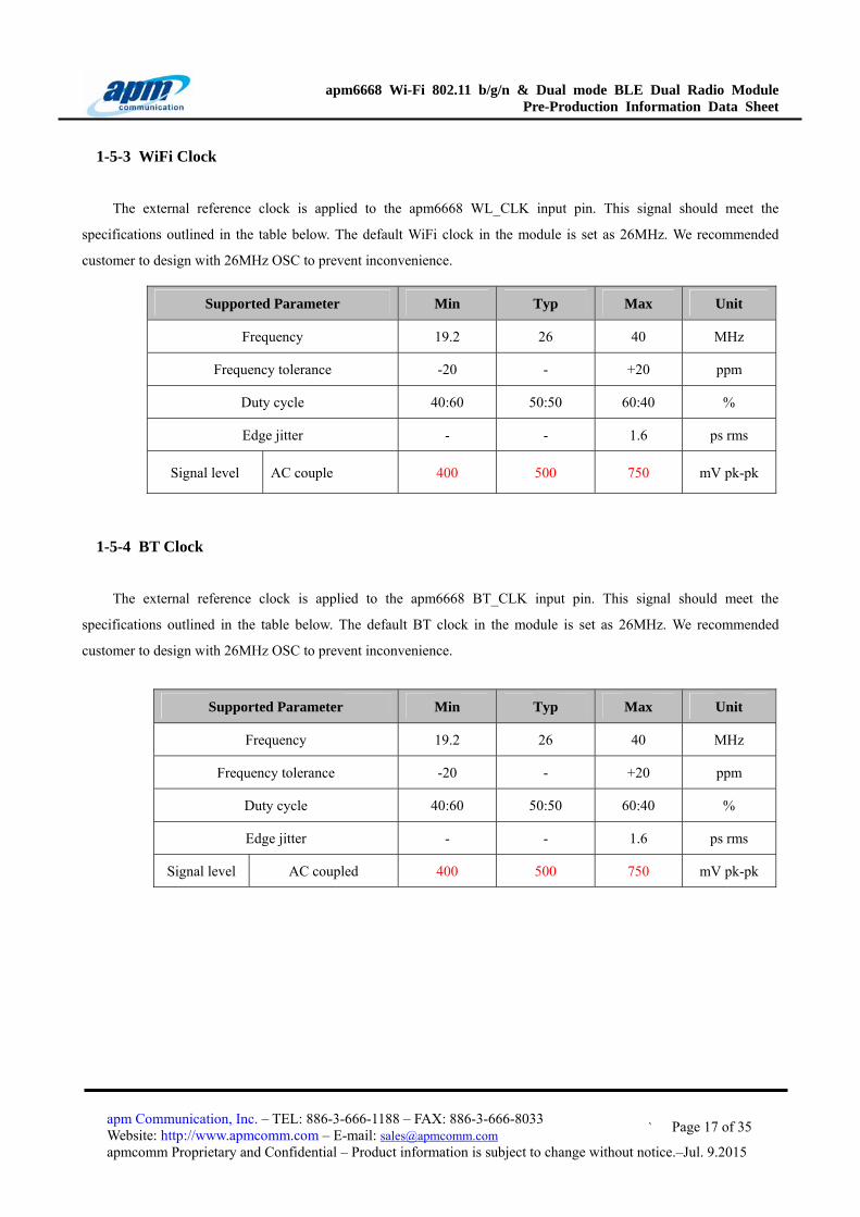
1-5-3 WiFi Clock
The external reference clock is applied to the apm6668 WL_CLK input pin. This signal should meet the
specifications outlined in the table below. The default WiFi clock in the module is set as 26MHz. We recommended
customer to design with 26MHz OSC to prevent inconvenience.
Supported Parameter Min Typ Max Unit
Frequency 19.2 26 40 MHz
Frequency tolerance -20 - +20 ppm
Duty cycle 40:60 50:50 60:40 %
Edge jitter - - 1.6 ps rms
Signal level AC couple 400 500 750 mV pk-pk
1-5-4 BT Clock
The external reference clock is applied to the apm6668 BT_CLK input pin. This signal should meet the
specifications outlined in the table below. The default BT clock in the module is set as 26MHz. We recommended
customer to design with 26MHz OSC to prevent inconvenience.
Supported Parameter Min Typ Max Unit
Frequency 19.2 26 40 MHz
Frequency tolerance -20 - +20 ppm
Duty cycle 40:60 50:50 60:40 %
Edge jitter - - 1.6 ps rms
Signal level AC coupled 400 500 750 mV pk-pk
apm6668 Wi-Fi 802.11 b/g/n & Dual mode BLE Dual Radio Module Pre-Production Information Data Sheet
` Page 18 of 35 apm Communication, Inc. – TEL: 886-3-666-1188 – FAX: 886-3-666-8033 Website: http://www.apmcomm.com – E-mail: [email protected] apmcomm Proprietary and Confidential – Product information is subject to change without notice.–Jul. 9.2015
1-5-5 BT Sleep Clock
The sleep clock is an external 32.768kHz clock for deep sleep and other low-power modes. This signal should
meet the specifications outlined in the table below.
Note:Sleep clock can be input on BT_CLK32K Pin.
Supported Parameter Min Typ Max Unit
Frequency 32.748 32.768 32.788 KHz
Frequency tolerance -25 - +25 ppm
Duty cycle 40:60 50:50 60:40 %
Edge jitter - - 10 ns rms
VIL -0.4 - +0.4
Signal level
VIH 0.8* BT_VDD_PADS - BT_VDD_PADS+0.3
V
apm6668 Wi-Fi 802.11 b/g/n & Dual mode BLE Dual Radio Module Pre-Production Information Data Sheet
` Page 19 of 35 apm Communication, Inc. – TEL: 886-3-666-1188 – FAX: 886-3-666-8033 Website: http://www.apmcomm.com – E-mail: [email protected] apmcomm Proprietary and Confidential – Product information is subject to change without notice.–Jul. 9.2015
1-6 Electrical Specifications
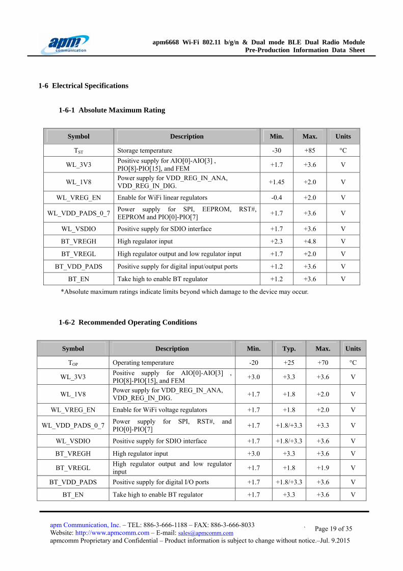
1-6-1 Absolute Maximum Rating
Symbol Description Min. Max. Units
TST Storage temperature -30 +85 °C
WL_3V3 Positive supply for AIO[0]-AIO[3] , PIO[8]-PIO[15], and FEM +1.7 +3.6 V
WL_1V8 Power supply for VDD_REG_IN_ANA, VDD_REG_IN_DIG. +1.45 +2.0 V
WL_VREG_EN Enable for WiFi linear regulators -0.4 +2.0 V
WL_VDD_PADS_0_7 Power supply for SPI, EEPROM, RST#, EEPROM and PIO[0]-PIO[7] +1.7 +3.6 V
WL_VSDIO Positive supply for SDIO interface +1.7 +3.6 V
BT_VREGH High regulator input +2.3 +4.8 V
BT_VREGL High regulator output and low regulator input +1.7 +2.0 V
BT_VDD_PADS Positive supply for digital input/output ports +1.2 +3.6 V
BT_EN Take high to enable BT regulator +1.2 +3.6 V
*Absolute maximum ratings indicate limits beyond which damage to the device may occur.
1-6-2 Recommended Operating Conditions
Symbol Description Min. Typ. Max. Units
TOP Operating temperature -20 +25 +70 °C
WL_3V3 Positive supply for AIO[0]-AIO[3] , PIO[8]-PIO[15], and FEM +3.0 +3.3 +3.6 V
WL_1V8 Power supply for VDD_REG_IN_ANA, VDD_REG_IN_DIG. +1.7 +1.8 +2.0 V
WL_VREG_EN Enable for WiFi voltage regulators +1.7 +1.8 +2.0 V
WL_VDD_PADS_0_7 Power supply for SPI, RST#, and PIO[0]-PIO[7] +1.7 +1.8/+3.3 +3.3 V
WL_VSDIO Positive supply for SDIO interface +1.7 +1.8/+3.3 +3.6 V
BT_VREGH High regulator input +3.0 +3.3 +3.6 V
BT_VREGL High regulator output and low regulator input +1.7 +1.8 +1.9 V
BT_VDD_PADS Positive supply for digital I/O ports +1.7 +1.8/+3.3 +3.6 V
BT_EN Take high to enable BT regulator +1.7 +3.3 +3.6 V
apm6668 Wi-Fi 802.11 b/g/n & Dual mode BLE Dual Radio Module Pre-Production Information Data Sheet
` Page 20 of 35 apm Communication, Inc. – TEL: 886-3-666-1188 – FAX: 886-3-666-8033 Website: http://www.apmcomm.com – E-mail: [email protected] apmcomm Proprietary and Confidential – Product information is subject to change without notice.–Jul. 9.2015
MCS7 transmit@+12dBm Continuous packet, PSDU length of
4096 Bytes mA -
121/ 3V3
132/ 1V8 -
MCS7 receive -68dBm. Continuous packet, PSDU
length of 4096 Bytes mA -
10/ 3V3
130/ 1V8 -
Listen Receive but no OFDM/CCK packet in
air mA -
10/3V3
140/1V8 -
Sleep Current Consumption
Deep sleep uA - 13/3V3
75/1V8 -
apm6668 Wi-Fi 802.11 b/g/n & Dual mode BLE Dual Radio Module Pre-Production Information Data Sheet
` Page 21 of 35 apm Communication, Inc. – TEL: 886-3-666-1188 – FAX: 886-3-666-8033 Website: http://www.apmcomm.com – E-mail: [email protected] apmcomm Proprietary and Confidential – Product information is subject to change without notice.–Jul. 9.2015
apm6668 Wi-Fi 802.11 b/g/n & Dual mode BLE Dual Radio Module Pre-Production Information Data Sheet
` Page 22 of 35 apm Communication, Inc. – TEL: 886-3-666-1188 – FAX: 886-3-666-8033 Website: http://www.apmcomm.com – E-mail: [email protected] apmcomm Proprietary and Confidential – Product information is subject to change without notice.–Jul. 9.2015
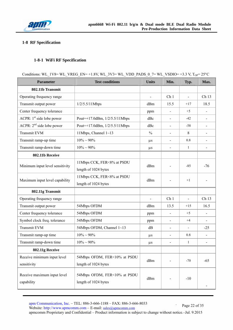
Transmit output power 1/2/5.5/11Mbps dBm 15.5 +17 18.5
Center frequency tolerance ppm - +5 -
ACPR: 1st side lobe power Pout=+17.0dBm, 1/2/5.5/11Mbps dBc - -42 -
ACPR: 2nd side lobe power Pout=+17.0dBm, 1/2/5.5/11Mbps dBc - -58 -
Transmit EVM 11Mbps, Channel 1~13 % - 8 -
Transmit ramp-up time 10% ~ 90% μs - 0.8 -
Transmit ramp-down time 10% ~ 90% μs - 1 -
802.11b Receive
Minimum input level sensitivity 11Mbps CCK, FER<8% at PSDU
length of 1024 bytes dBm - -85 -76
Maximum input level capability 11Mbps CCK, FER<8% at PSDU
length of 1024 bytes dBm - +1 -
802.11g Transmit
Operating frequency range - Ch 1 - Ch 13
Transmit output power 54Mbps OFDM dBm 13.5 +15 16.5
Center frequency tolerance 54Mbps OFDM ppm - +5 -
Symbol clock freq. tolerance 54Mbps OFDM ppm - +4 -
Transmit EVM 54Mbps OFDM, Channel 1~13 dB - - -25
Transmit ramp-up time 10% ~ 90% μs - 0.8 -
Transmit ramp-down time 10% ~ 90% μs - 1 -
802.11g Receive
Receive minimum input level
sensitivity
54Mbps OFDM, FER<10% at PSDU
length of 1024 bytes dBm - -70 -65
Receive maximum input level
capability
54Mbps OFDM, FER<10% at PSDU
length of 1024 bytes dBm - -10
-
apm6668 Wi-Fi 802.11 b/g/n & Dual mode BLE Dual Radio Module Pre-Production Information Data Sheet
` Page 23 of 35 apm Communication, Inc. – TEL: 886-3-666-1188 – FAX: 886-3-666-8033 Website: http://www.apmcomm.com – E-mail: [email protected] apmcomm Proprietary and Confidential – Product information is subject to change without notice.–Jul. 9.2015
apm6668 Wi-Fi 802.11 b/g/n & Dual mode BLE Dual Radio Module Pre-Production Information Data Sheet
` Page 24 of 35 apm Communication, Inc. – TEL: 886-3-666-1188 – FAX: 886-3-666-8033 Website: http://www.apmcomm.com – E-mail: [email protected] apmcomm Proprietary and Confidential – Product information is subject to change without notice.–Jul. 9.2015
apm6668 Wi-Fi 802.11 b/g/n & Dual mode BLE Dual Radio Module Pre-Production Information Data Sheet
` Page 25 of 35 apm Communication, Inc. – TEL: 886-3-666-1188 – FAX: 886-3-666-8033 Website: http://www.apmcomm.com – E-mail: [email protected] apmcomm Proprietary and Confidential – Product information is subject to change without notice.–Jul. 9.2015
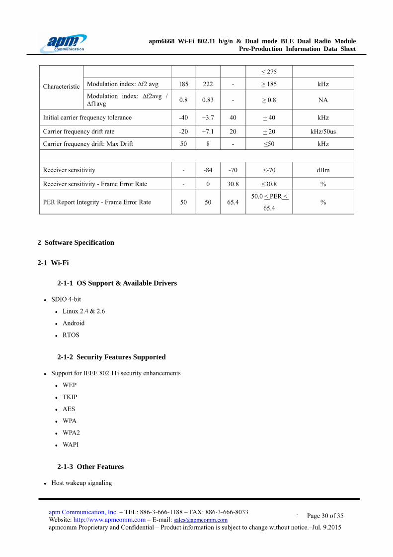
Initial carrier frequency tolerance -35 +9.1 35 + 35 kHz
Carrier frequency drift rate -20 -9. 20 + 20 kHz/50us
apm6668 Wi-Fi 802.11 b/g/n & Dual mode BLE Dual Radio Module Pre-Production Information Data Sheet
` Page 26 of 35 apm Communication, Inc. – TEL: 886-3-666-1188 – FAX: 886-3-666-8033 Website: http://www.apmcomm.com – E-mail: [email protected] apmcomm Proprietary and Confidential – Product information is subject to change without notice.–Jul. 9.2015
Parameter Min Typ Max Bluetooth Spec. Unit
Carrier frequency drift: one slot packet -25 -4.3 25 + 25 kHz
Carrier frequency drift: three slot packet -40 +6.6 40 + 40 kHz
Carrier frequency drift: five slot packet -40 -8.4 40 + 40 kHz
apm6668 Wi-Fi 802.11 b/g/n & Dual mode BLE Dual Radio Module Pre-Production Information Data Sheet
` Page 27 of 35 apm Communication, Inc. – TEL: 886-3-666-1188 – FAX: 886-3-666-8033 Website: http://www.apmcomm.com – E-mail: [email protected] apmcomm Proprietary and Confidential – Product information is subject to change without notice.–Jul. 9.2015
Parameter Min Typ Max Bluetooth Spec. Unit
BER 8 DPSK - -74 -70 <-70
EDR Floor Performance - 0 - 7.00E-006
1.00E-005
EDR MAX input power 0 1.00E-003
*(a) RF TX Power can be set by PSR setting.
Channel 78 (2480MHz)
Parameter Min Typ Max Bluetooth Spec. Unit
Basic Data Rate - Transmitter Test
Maximum RF transmit power *(a) -6 - +4 Class1: 0 to +20
apm6668 Wi-Fi 802.11 b/g/n & Dual mode BLE Dual Radio Module Pre-Production Information Data Sheet
` Page 28 of 35 apm Communication, Inc. – TEL: 886-3-666-1188 – FAX: 886-3-666-8033 Website: http://www.apmcomm.com – E-mail: [email protected] apmcomm Proprietary and Confidential – Product information is subject to change without notice.–Jul. 9.2015
Parameter Min Typ Max Bluetooth Spec. Unit
Max carrier frequency stability〡ωo+ωi〡 for all blocks
8 DPSK
Max carrier frequency stability ωi -75 +4.4 75
< +75
for all packets kHz
8 DPSK Max carrier frequency stability ωo
-10 -1.7 10 < +10
for all blocks kHz
8 DPSK
Max carrier frequency stability〡ωo+ωi〡 -75 +4.8 75
apm6668 Wi-Fi 802.11 b/g/n & Dual mode BLE Dual Radio Module Pre-Production Information Data Sheet
` Page 29 of 35 apm Communication, Inc. – TEL: 886-3-666-1188 – FAX: 886-3-666-8033 Website: http://www.apmcomm.com – E-mail: [email protected] apmcomm Proprietary and Confidential – Product information is subject to change without notice.–Jul. 9.2015
∆f1avg
Initial carrier frequency tolerance -40 +2.4 40 + 40 kHz
Carrier frequency drift rate -20 +7.3 20 + 20 kHz/50us
apm6668 Wi-Fi 802.11 b/g/n & Dual mode BLE Dual Radio Module Pre-Production Information Data Sheet
` Page 30 of 35 apm Communication, Inc. – TEL: 886-3-666-1188 – FAX: 886-3-666-8033 Website: http://www.apmcomm.com – E-mail: [email protected] apmcomm Proprietary and Confidential – Product information is subject to change without notice.–Jul. 9.2015
PER Report Integrity - Frame Error Rate 50 50 65.4 50.0 < PER <
65.4 %
2 Software Specification
2-1 Wi-Fi
2-1-1 OS Support & Available Drivers
SDIO 4-bit Linux 2.4 & 2.6 Android RTOS
2-1-2 Security Features Supported
Support for IEEE 802.11i security enhancements
WEP
TKIP
AES
WPA
WPA2
WAPI
2-1-3 Other Features
Host wakeup signaling
apm6668 Wi-Fi 802.11 b/g/n & Dual mode BLE Dual Radio Module Pre-Production Information Data Sheet
` Page 31 of 35 apm Communication, Inc. – TEL: 886-3-666-1188 – FAX: 886-3-666-8033 Website: http://www.apmcomm.com – E-mail: [email protected] apmcomm Proprietary and Confidential – Product information is subject to change without notice.–Jul. 9.2015
Soft AP (for Linux and Android)
WIFI Direct
2-2 Bluetooth Software Stacks
apm6668 is supplied with Bluetooth v4.0+EDR compliant stack firmware, which runs on internal RISC
microcontroller.
2-2-1 HCI Stack
All Bluetooth v2.1+EDR mandatory and optional features are supported. The firmware also extends the standard
Bluetooth functionality with numerous features. Please contact apmcomm FAE for details.
2-2-2 Host Software
BlueCore Embedded Host Software (BCHS). About the Host Software, please contact apmcomm FAE for details.
apm6668 Wi-Fi 802.11 b/g/n & Dual mode BLE Dual Radio Module Pre-Production Information Data Sheet
` Page 32 of 35 apm Communication, Inc. – TEL: 886-3-666-1188 – FAX: 886-3-666-8033 Website: http://www.apmcomm.com – E-mail: [email protected] apmcomm Proprietary and Confidential – Product information is subject to change without notice.–Jul. 9.2015
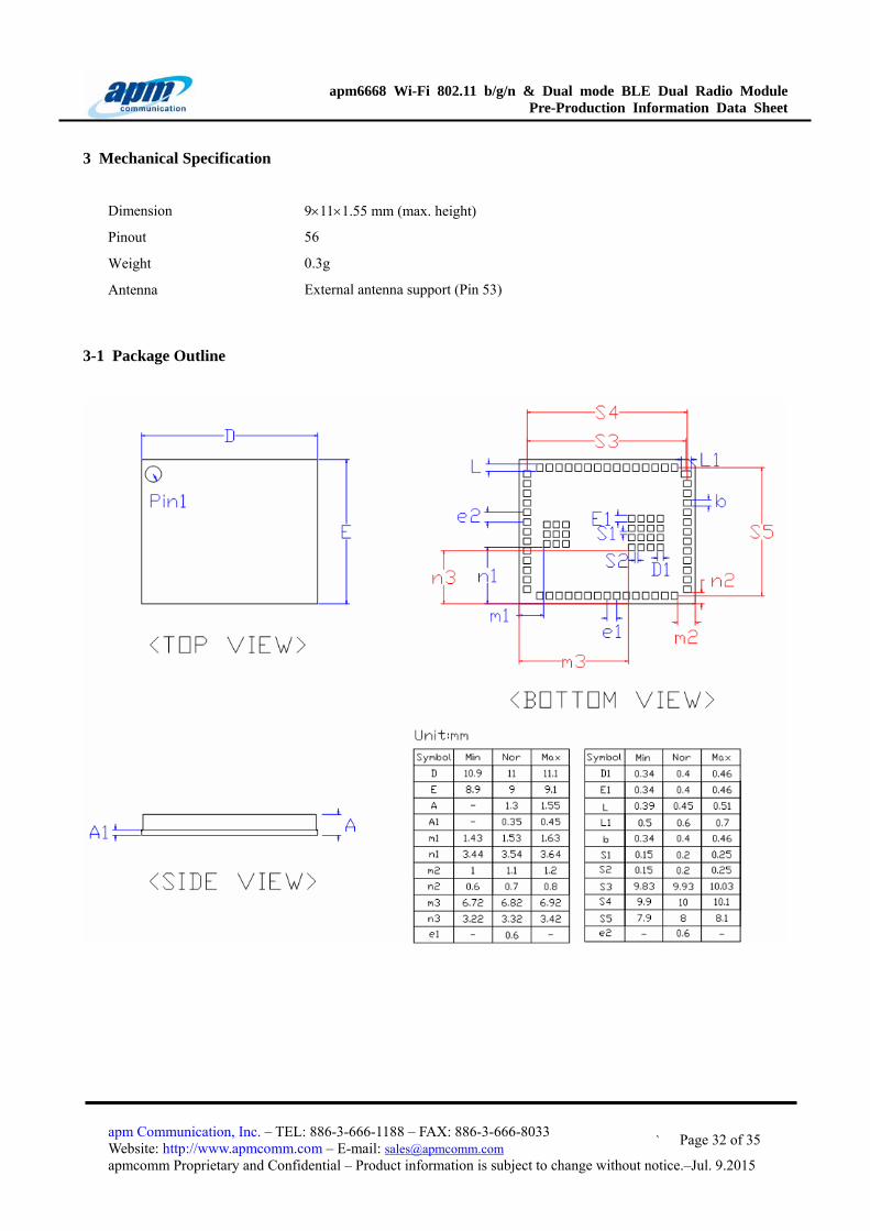
3 Mechanical Specification
Dimension 9×11×1.55 mm (max. height)
Pinout 56
Weight 0.3g
Antenna External antenna support (Pin 53)
3-1 Package Outline
apm6668 Wi-Fi 802.11 b/g/n & Dual mode BLE Dual Radio Module Pre-Production Information Data Sheet
` Page 33 of 35 apm Communication, Inc. – TEL: 886-3-666-1188 – FAX: 886-3-666-8033 Website: http://www.apmcomm.com – E-mail: [email protected] apmcomm Proprietary and Confidential – Product information is subject to change without notice.–Jul. 9.2015
4 Assembly Guideline
4-1 Recommended Mounting Pad Design (Top View)
The following figure illustrates the recommended mounting pad design for apm6668.
TOP VIEW (mm)
4-2 Recommendation for Stencil Aperture in SMT Process
Please follow general QFN stencil design guideline. Some rules of thumb are highlighted below.
‧ The LGA pads should NOT be flooded over with copper, they should be connected into the plane with a track
width of approx 50% of the pad width, this will mean more heat will be available at the joint. Track lengths should
obviously be minimized, we would generally use about 0.3mm on external layers.
apm6668 Wi-Fi 802.11 b/g/n & Dual mode BLE Dual Radio Module Pre-Production Information Data Sheet
` Page 34 of 35 apm Communication, Inc. – TEL: 886-3-666-1188 – FAX: 886-3-666-8033 Website: http://www.apmcomm.com – E-mail: [email protected] apmcomm Proprietary and Confidential – Product information is subject to change without notice.–Jul. 9.2015
‧ The solder paste pattern for the internal Tab pads could be split into 4 smaller segments for the 2 large pads, and
2 smaller segments for the smaller pads, this should have the effect of preventing the paste from pooling into one area,
and hence minimize the likelihood of the pads being held away from each other. We use a rule of thumb of 50% solder
paste area in relation to Tab copper area (this only applies to tab pads under the device – not the signal pads).
‧ The thickness of the solder paste stencil has implications on solder joint quality as well, we do not have the
knowledge on what stencil should be specified.
‧ Ensure they are using a good appropriate flux, and the correct reflow profile for unleaded (basically +20C above
leaded) which is also uniform in nature.
Violating the basic rules might cause problems. For example, if the stencil apertures of the internal ground planes
are improperly big, they would hold more solders in SMT process and may cause the module peripheral pads
un-contacted to the main board. To improve this situation, apmcomm suggests the stencil opening shown as follows.
Stencil Aperture (Top View)
apm6668 Wi-Fi 802.11 b/g/n & Dual mode BLE Dual Radio Module Pre-Production Information Data Sheet
` Page 35 of 35 apm Communication, Inc. – TEL: 886-3-666-1188 – FAX: 886-3-666-8033 Website: http://www.apmcomm.com – E-mail: [email protected] apmcomm Proprietary and Confidential – Product information is subject to change without notice.–Jul. 9.2015
4-3 Baking condition recommendation before IR reflow
Baking condition for apm6668 module:
I: 125°C/4 hrs baking is necessary for apm6668 module before SMT process. After baking treatment the modules
can be stored in the environment under 30°C and 60% RH for 168 hrs. If the storage time is over 168 hrs, the
modules need to be re-baked using the same condition again.
II: In the event that the sealed bag is damaged on receipt of the modules, the baking condition should be changed to 125°C/8 hrs.
4-4 Recommendation for Reflow Profile
Maximum reflow temperature is 250°C.
Preheat ramp-up rate 125°C to 180°C 1 to 3°C /sec.
Peak temperature 250°C max. Temperature maintained above 217°C 30 ~ 90 sec. Cooling ramp-down rate <2°C/sec. Maximum number of reflow cycles ≤3
Heating/Cooling Speed Pre-Heating Heating
ΔT1 ΔT2 ΔT3 Tp1−Tp2 tpre TMax tP3
1 to 3°C /sec. 1 to 3°C /sec. < 2°C /sec. 125 ~ 180°C 30 ~ 90 sec. 250°C max. 30 ~ 90 sec.