16-Bit, Voltage Output, Serial InputDIGITAL-TO-ANALOG CONVERTER
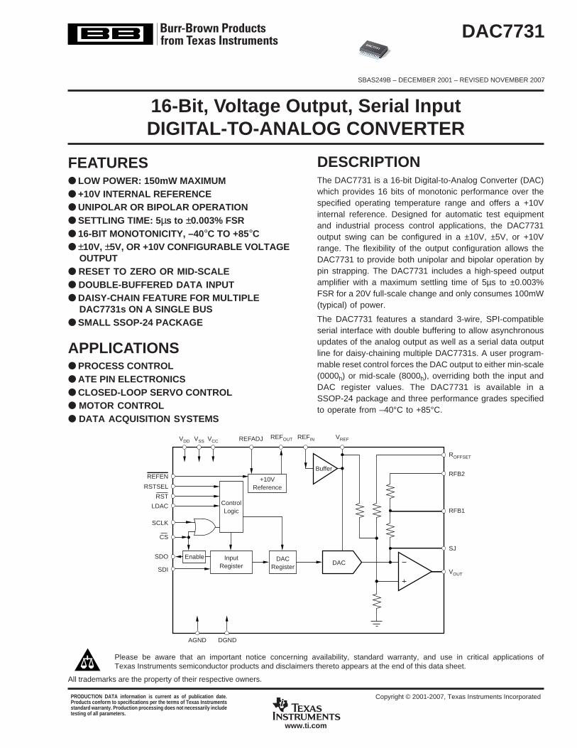
DESCRIPTIONThe DAC7731 is a 16-bit Digital-to-Analog Converter (DAC)which provides 16 bits of monotonic performance over thespecified operating temperature range and offers a +10Vinternal reference. Designed for automatic test equipmentand industrial process control applications, the DAC7731output swing can be configured in a ±10V, ±5V, or +10Vrange. The flexibility of the output configuration allows theDAC7731 to provide both unipolar and bipolar operation bypin strapping. The DAC7731 includes a high-speed outputamplifier with a maximum settling time of 5µs to ±0.003%FSR for a 20V full-scale change and only consumes 100mW(typical) of power.
The DAC7731 features a standard 3-wire, SPI-compatibleserial interface with double buffering to allow asynchronousupdates of the analog output as well as a serial data outputline for daisy-chaining multiple DAC7731s. A user program-mable reset control forces the DAC output to either min-scale(0000h) or mid-scale (8000h), overriding both the input andDAC register values. The DAC7731 is available in aSSOP-24 package and three performance grades specifiedto operate from –40°C to +85°C.
FEATURES LOW POWER: 150mW MAXIMUM +10V INTERNAL REFERENCE UNIPOLAR OR BIPOLAR OPERATION SETTLING TIME: 5µs to ±0.003% FSR 16-BIT MONOTONICITY, –40°C TO +85°C ±10V, ±5V, OR +10V CONFIGURABLE VOLTAGE
OUTPUT RESET TO ZERO OR MID-SCALE DOUBLE-BUFFERED DATA INPUT DAISY-CHAIN FEATURE FOR MULTIPLE
DAC7731s ON A SINGLE BUS SMALL SSOP-24 PACKAGE
APPLICATIONS PROCESS CONTROL ATE PIN ELECTRONICS CLOSED-LOOP SERVO CONTROL MOTOR CONTROL DATA ACQUISITION SYSTEMS
Please be aware that an important notice concerning availability, standard warranty, and use in critical applications ofTexas Instruments semiconductor products and disclaimers thereto appears at the end of this data sheet.
Buffer
+10VReference
ControlLogic
Enable InputRegister
DACRegister
DAC
REFEN
RSTSEL
RST
LDAC
SCLK
CS
SDO
SDI
VDD VSS VCC REFADJ REFOUT REFIN VREF
ROFFSET
RFB2
RFB1
SJ
VOUT
AGND DGND
DAC7731
PRODUCTION DATA information is current as of publication date.Products conform to specifications per the terms of Texas Instrumentsstandard warranty. Production processing does not necessarily includetesting of all parameters.
All trademarks are the property of their respective owners.
DAC77312SBAS249Bwww.ti.com
ABSOLUTE MAXIMUM RATINGS(1)
VCC to VSS ........................................................................... –0.3V to +32VVCC to AGND ...................................................................... –0.3V to +16VVSS to AGND ...................................................................... –16V to +0.3VAGND to DGND ................................................................... –0.3V to 0.3VREFIN to AGND .............................................................. 0V to VCC – 1.4VVDD to DGND ........................................................................ –0.3V to +6VDigital Input Voltage to DGND ................................. –0.3V to VDD + 0.3VDigital Output Voltage to DGND .............................. –0.3V to VDD + 0.3VOperating Temperature Range ........................................ –40°C to +85°CStorage Temperature Range ......................................... –65°C to +150°CJunction Temperature (TJ Max) .................................................... +150°C
NOTE: (1) Stresses above those listed under Absolute Maximum Ratings maycause permanent damage to the device. Exposure to absolute maximumconditions for extended periods may affect device reliability.
ELECTROSTATICDISCHARGE SENSITIVITY
This integrated circuit can be damaged by ESD. Texas Instru-ments recommends that all integrated circuits be handled withappropriate precautions. Failure to observe proper handlingand installation procedures can cause damage.
ESD damage can range from subtle performance degradationto complete device failure. Precision integrated circuits may bemore susceptible to damage because very small parametricchanges could cause the device not to meet its publishedspecifications.
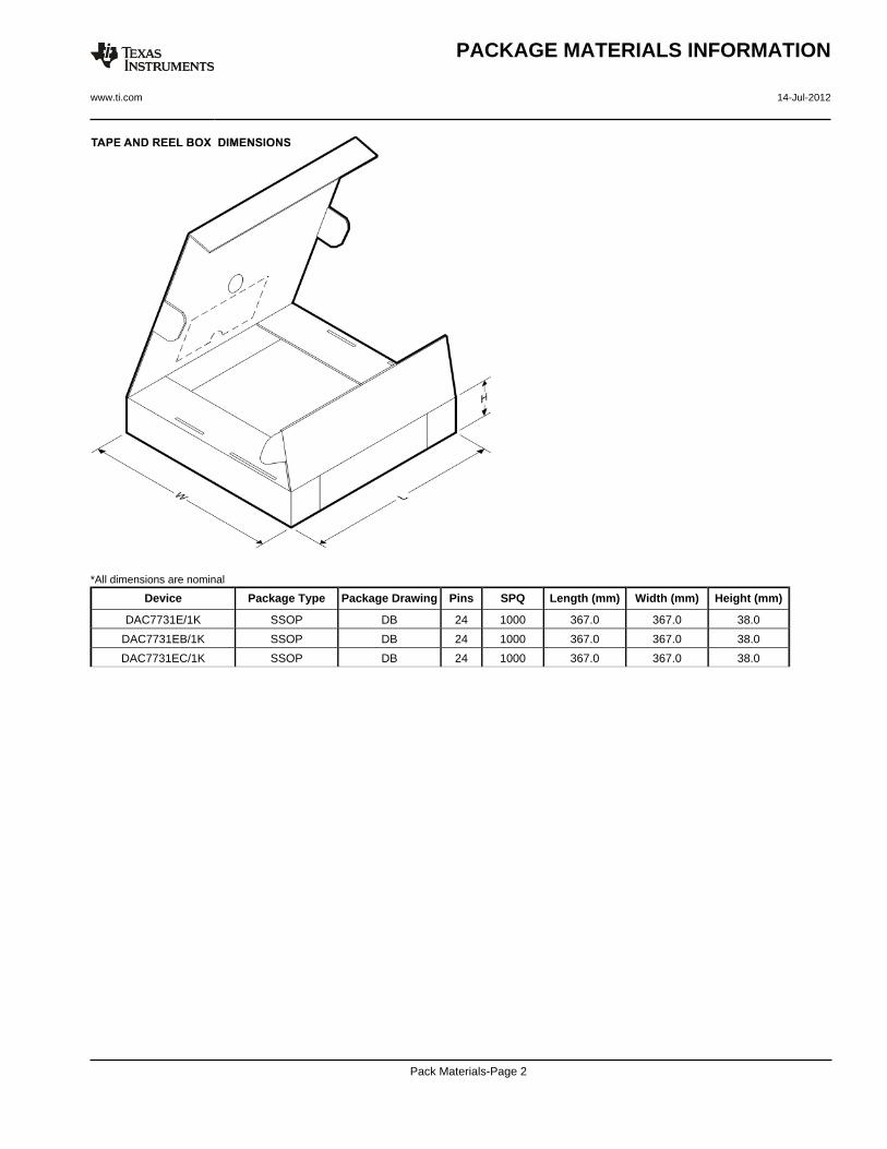
PACKAGE/ORDERING INFORMATION(1)
SPECIFIEDPACKAGE TEMPERATURE PACKAGE ORDERING TRANSPORT
PRODUCT PACKAGE-LEAD DESIGNATOR RANGE MARKING NUMBER(2) MEDIA, QUANTITY
DAC7731E SSOP-24 DB –40°C to +85°C DAC7731E DAC7731E Rails, 60" " " " " DAC7731E/1K Tape and Reel,1000
DAC7731EB SSOP-24 DB –40°C to +85°C DAC7731EB DAC7731EB Rails, 60" " " " " DAC7731EB/1K Tape and Reel, 1000
DAC7731EC SSOP-24 DB –40°C to +85°C DAC7731EC DAC7731EC Rails, 60" " " " " DAC7731EC/1K Tape and Reel, 1000
NOTE: (1) For the most current package ordering information, see the Package Option Addendum at the end of this data sheet, or see the TI web site at www.ti.com.
Top View SSOP
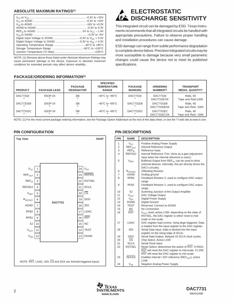
PIN CONFIGURATION
PIN NAME DESCRIPTION
1 VCC Positive Analog Power Supply2 REFOUT Internal Reference Output3 REFIN Reference Input4 REFADJ Internal Reference Trim. (Acts as a gain adjustment
input when the internal reference is used.)5 VREF Buffered Output from REFIN, can be used to drive
external devices. Internally, this pin directly drives theDAC's circuitry.
6 ROFFSET Offsetting Resistor7 AGND Analog ground8 RFB2 Feedback Resistor 2, used to configure DAC output
range.9 RFB1 Feedback Resistor 1, used to configure DAC output
range.10 SJ Summing Junction of the Output Amplifier11 VOUT DAC Voltage Output12 VDD Digital Power Supply13 DGND Digital Ground14 TEST Reserved, Connect to DGND15 NC No Connection16 RST VOUT reset; active LOW, depending on the state of
RSTSEL, the DAC register is either reset to mid-scale or min-scale.
17 LDAC DAC register load control, rising dege triggered. Datais loaded from the input register to the DAC register.
18 SDI Serial Data Input. Data is latched into the inputregister on the rising edge of SCLK.
19 SDO Serial Data Output, delayed 16 SCLK clock cycles.20 CS Chip Select, Active LOW21 SCLK Serial Clock Input22 RSTSEL Reset Select; determines the action of RST. If HIGH,
RST will reset the DAC register to mid-scale. If LOW,RST will reset the DAC register to min-scale.
NOTES: (1) With minimum VCC/VSS requirements, internal reference enabled.(2) Please refer to the Theory of Operation section for more information with respect to output voltage configurations.(3) See Figure 11 for gain and offset adjustment connection diagrams when using the internal reference.(4) The minimum value for REFIN must be equal to the greater of VSS +14V and +4.75V, where +4.75V is the minimum voltage allowed.(5) Reference low-pass filter values: 100kΩ, 1.0µF (see Figure 14).
ELECTRICAL CHARACTERISTICSAll specifications at TA = TMIN to TMAX, VCC = +15V, VSS = –15V, VDD = +5V, Internal refi⁄ence enabled, unless otherwise noted.
DAC77314SBAS249Bwww.ti.com
PARAMETER DESCRIPTION MIN TYP MAX UNITS
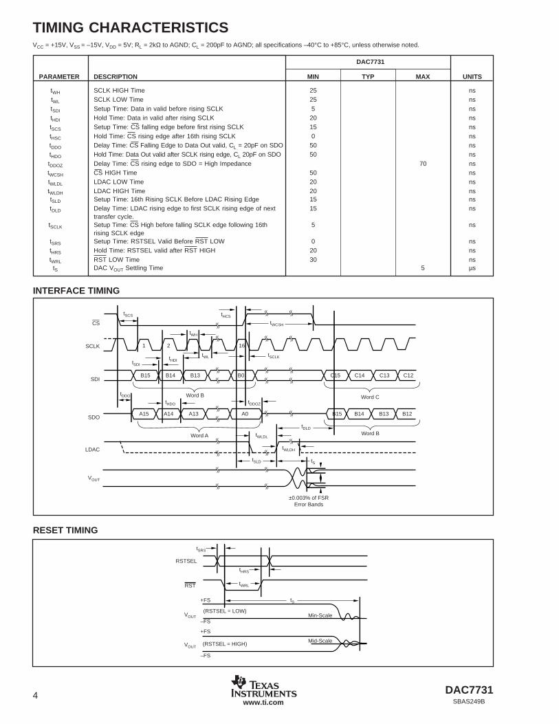
tWH SCLK HIGH Time 25 nstWL SCLK LOW Time 25 nstSDI Setup Time: Data in valid before rising SCLK 5 nstHDI Hold Time: Data in valid after rising SCLK 20 nstSCS Setup Time: CS falling edge before first rising SCLK 15 nstHSC Hold Time: CS rising edge after 16th rising SCLK 0 nstDDO Delay Time: CS Falling Edge to Data Out valid, CL = 20pF on SDO 50 nstHDO Hold Time: Data Out valid after SCLK rising edge, CL 20pF on SDO 50 nstDDOZ Delay Time: CS rising edge to SDO = High Impedance 70 nstWCSH CS HIGH Time 50 nstWLDL LDAC LOW Time 20 nstWLDH LDAC HIGH Time 20 nstSLD Setup Time: 16th Rising SCLK Before LDAC Rising Edge 15 nstDLD Delay Time: LDAC rising edge to first SCLK rising edge of next 15 ns
transfer cycle.tSCLK Setup Time: CS High before falling SCLK edge following 16th 5 ns
rising SCLK edgetSRS Setup Time: RSTSEL Valid Before RST LOW 0 nstHRS Hold Time: RSTSEL valid after RST HIGH 20 nstWRL RST LOW Time 30 nstS DAC VOUT Settling Time 5 µs
TIMING CHARACTERISTICSVCC = +15V, VSS = –15V, VDD = 5V; RL = 2kΩ to AGND; CL = 200pF to AGND; all specifications –40°C to +85°C, unless otherwise noted.
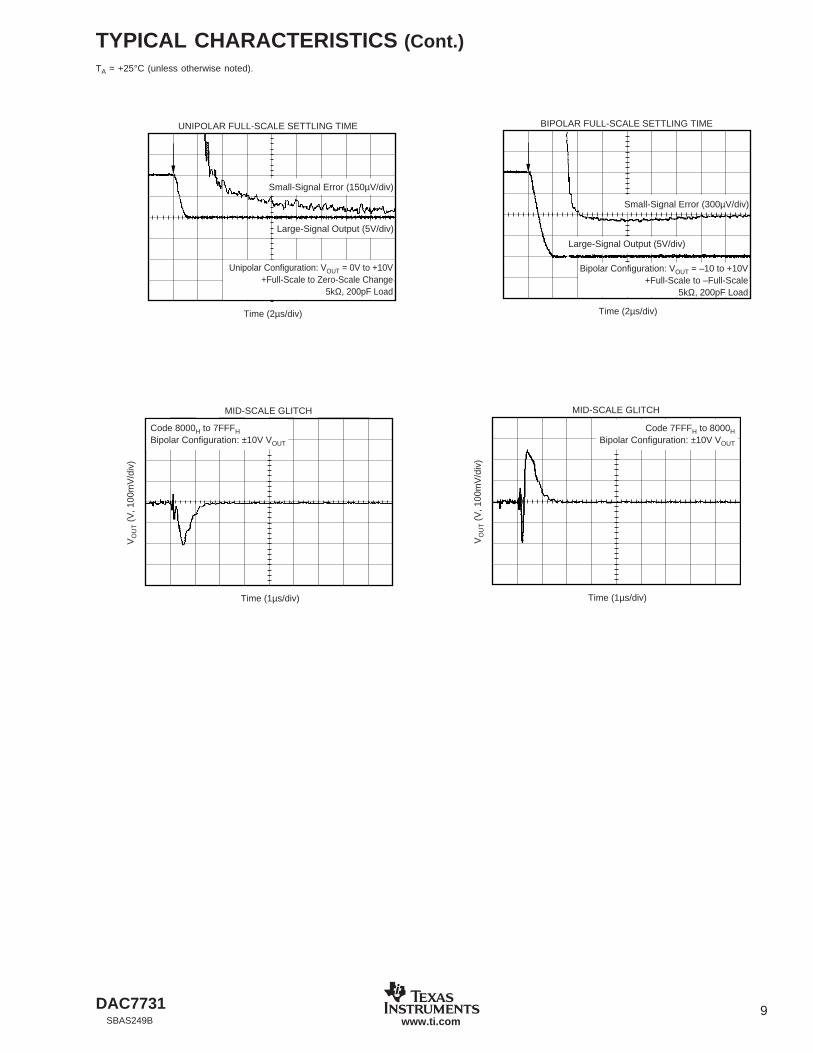
Unipolar Configuration: VOUT = 0V to +10V+Full-Scale to Zero-Scale Change
5kΩ, 200pF Load
Large-Signal Output (5V/div)
UNIPOLAR FULL-SCALE SETTLING TIME
Time (2µs/div)
Small-Signal Error (150µV/div)
Bipolar Configuration: VOUT = –10 to +10V+Full-Scale to –Full-Scale
5kΩ, 200pF Load
Large-Signal Output (5V/div)
BIPOLAR FULL-SCALE SETTLING TIME
Time (2µs/div)
Small-Signal Error (300µV/div)
Code 8000H to 7FFFHBipolar Configuration: ±10V VOUT
MID-SCALE GLITCH
Time (1µs/div)
VO
UT (
V, 1
00m
V/d
iv)
MID-SCALE GLITCH
Time (1µs/div)
VO
UT (
V, 1
00m
V/d
iv)
Code 7FFFH to 8000HBipolar Configuration: ±10V VOUT
DAC773110SBAS249Bwww.ti.com
VCC
REFOUT
REFIN
REFADJ
VREF
ROFFSET
AGND
RFB2
RFB1
SJ
VOUT
VDD
VSS
REFEN
RSTSEL
SCLK
CS
SDO
SDI
LDAC
RST
NC
TEST
DGND
1
2
3
4
5
6
7
8
9
10
11
12
24
23
22
21
20
19
18
17
16
15
14
13
DAC77311µF0.1µF
VCC
1µF0.1µF
VDD
Control/DataBus
1µF 0.1µF
VSS
(–5V to +5V)
FIGURE 3. Basic Operation: VOUT = –5V to +5V.
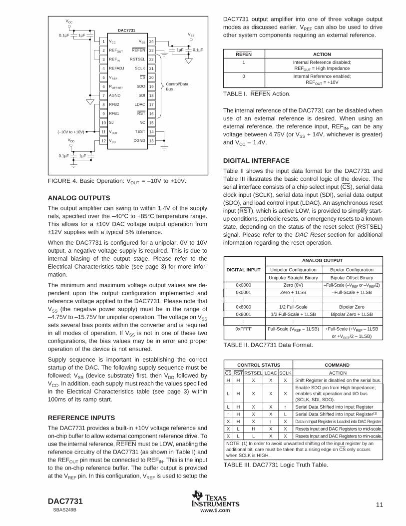
THEORY OF OPERATIONThe DAC7731 is a voltage output, 16-bit DAC with a +10Vbuilt-in internal reference. The architecture is an R-2R ladderconfiguration with the three MSBs segmented, followed byan operational amplifier that serves as a buffer, as shown inFigure 1. The output buffer is designed to allow user-configurable output adjustments giving the DAC7731 outputvoltage ranges of 0V to +10V, –5V to +5V, or –10V to +10V.Please refer to Figures 2, 3, and 4 for pin configurationinformation.
The digital input is a serial word made up of the DAC code(MSB first) and is loaded into the DAC register using theLDAC input pin. The converter can be powered from ±12Vto ±15V dual analog supplies and a +5V logic supply. Thedevice offers a reset function, which immediately sets theDAC output voltage and DAC register to min-scale (code0000H) or mid-scale (code 8000H). The data I/O and resetfunctions are discussed in more detail in the following sec-tions.
FIGURE 1. DAC7731 Architecture.
FIGURE 2. Basic Operation: VOUT = 0V to +10V.
2R2R 2R 2R 2R 2R 2R 2R 2R
R/4
R/2R/2 R/4
R/4
R
ROFFSET
RFB2
RFB1
SJ
VOUT
VREF
VREF
AGND
REFINREFADJ REFOUT
+10V InternalReference
Buffer
VCC
REFOUT
REFIN
REFADJ
VREF
ROFFSET
AGND
RFB2
RFB1
SJ
VOUT
VDD
VSS
REFEN
RSTSEL
SCLK
CS
SDO
SDI
LDAC
RST
NC
TEST
DGND
1
2
3
4
5
6
7
8
9
10
11
12
24
23
22
21
20
19
18
17
16
15
14
13
DAC7731
1µF0.1µF
VCC
1µF0.1µF
VDD
Control/DataBus
1µF 0.1µF
VSS
(0V to +10V)
DAC7731 11SBAS249B www.ti.com
VCC
REFOUT
REFIN
REFADJ
VREF
ROFFSET
AGND
RFB2
RFB1
SJ
VOUT
VDD
VSS
REFEN
RSTSEL
SCLK
CS
SDO
SDI
LDAC
RST
NC
TEST
DGND
1
2
3
4
5
6
7
8
9
10
11
12
24
23
22
21
20
19
18
17
16
15
14
13
DAC77311µF0.1µF
VCC
1µF0.1µF
VDD
Control/DataBus
1µF 0.1µF
VSS
(–10V to +10V)
FIGURE 4. Basic Operation: VOUT = –10V to +10V.
ANALOG OUTPUTS
The output amplifier can swing to within 1.4V of the supplyrails, specified over the –40°C to +85°C temperature range.This allows for a ±10V DAC voltage output operation from±12V supplies with a typical 5% tolerance.
When the DAC7731 is configured for a unipolar, 0V to 10Voutput, a negative voltage supply is required. This is due tointernal biasing of the output stage. Please refer to theElectrical Characteristics table (see page 3) for more infor-mation.
The minimum and maximum voltage output values are de-pendent upon the output configuration implemented andreference voltage applied to the DAC7731. Please note thatVSS (the negative power supply) must be in the range of–4.75V to –15.75V for unipolar operation. The voltage on VSS
sets several bias points within the converter and is requiredin all modes of operation. If VSS is not in one of these twoconfigurations, the bias values may be in error and properoperation of the device is not ensured.
Supply sequence is important in establishing the correctstartup of the DAC. The following supply sequence must befollowed: VSS (device substrate) first, then VDD followed byVCC. In addition, each supply must reach the values specifiedin the Electrical Characteristics table (see page 3) within100ms of its ramp start.
REFERENCE INPUTS
The DAC7731 provides a built-in +10V voltage reference andon-chip buffer to allow external component reference drive. Touse the internal reference, REFEN must be LOW, enabling thereference circuitry of the DAC7731 (as shown in Table I) andthe REFOUT pin must be connected to REFIN. This is the inputto the on-chip reference buffer. The buffer output is providedat the VREF pin. In this configuration, VREF is used to setup the
REFEN ACTION
1 Internal Reference disabled;REFOUT = High Impedance
0 Internal Reference enabled;REFOUT = +10V
TABLE I. REFEN Action.
The internal reference of the DAC7731 can be disabled whenuse of an external reference is desired. When using anexternal reference, the reference input, REFIN, can be anyvoltage between 4.75V (or VSS + 14V, whichever is greater)and VCC – 1.4V.
DIGITAL INTERFACE
Table II shows the input data format for the DAC7731 andTable III illustrates the basic control logic of the device. Theserial interface consists of a chip select input (CS), serial dataclock input (SCLK), serial data input (SDI), serial data output(SDO), and load control input (LDAC). An asynchronous resetinput (RST), which is active LOW, is provided to simplify start-up conditions, periodic resets, or emergency resets to a knownstate, depending on the status of the reset select (RSTSEL)signal. Please refer to the DAC Reset section for additionalinformation regarding the reset operation.
CONTROL STATUS COMMAND
CS RST RSTSEL LDAC SCLK ACTION
H H X X X Shift Register is disabled on the serial bus.
Enable SDO pin from High Impedance;L H X X X enables shift operation and I/O bus
(SCLK, SDI, SDO).
L H X X ↑ Serial Data Shifted into Input Register
↑ H X X L Serial Data Shifted into Input Register(1)
X H X ↑ X Data in Input Register is Loaded into DAC Register.
X L H X X Resets Input and DAC Registers to mid-scale.
X L L X X Resets Input and DAC Registers to min-scale.
NOTE: (1) In order to avoid unwanted shifting of the input register by anadditional bit, care must be taken that a rising edge on CS only occurswhen SCLK is HIGH.
TABLE III. DAC7731 Logic Truth Table.
ANALOG OUTPUT
TABLE II. DAC7731 Data Format.
DIGITAL INPUT Unipolar Configuration Bipolar Configuration
DAC7731 output amplifier into one of three voltage outputmodes as discussed earlier. VREF can also be used to driveother system components requiring an external reference.
DAC773112SBAS249Bwww.ti.com
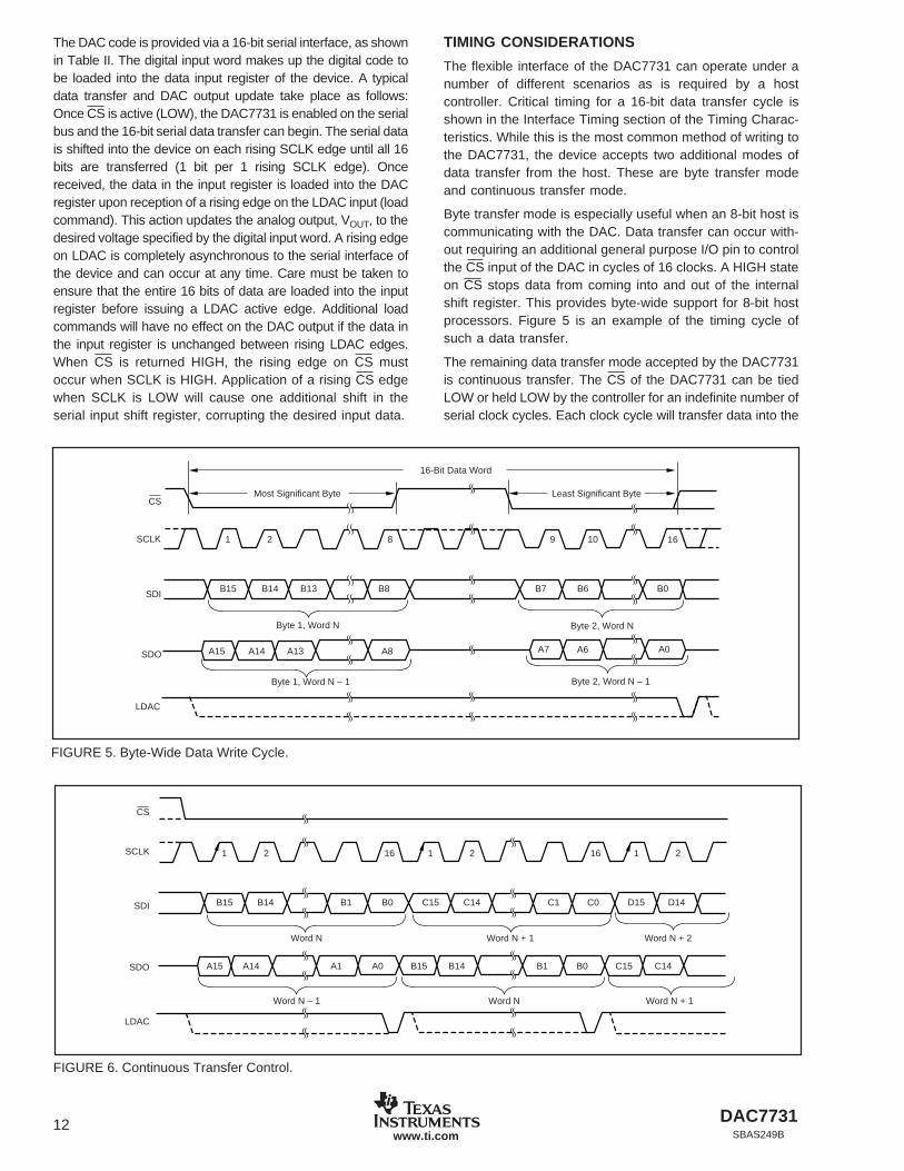
The DAC code is provided via a 16-bit serial interface, as shownin Table II. The digital input word makes up the digital code tobe loaded into the data input register of the device. A typicaldata transfer and DAC output update take place as follows:Once CS is active (LOW), the DAC7731 is enabled on the serialbus and the 16-bit serial data transfer can begin. The serial datais shifted into the device on each rising SCLK edge until all 16bits are transferred (1 bit per 1 rising SCLK edge). Oncereceived, the data in the input register is loaded into the DACregister upon reception of a rising edge on the LDAC input (loadcommand). This action updates the analog output, VOUT, to thedesired voltage specified by the digital input word. A rising edgeon LDAC is completely asynchronous to the serial interface ofthe device and can occur at any time. Care must be taken toensure that the entire 16 bits of data are loaded into the inputregister before issuing a LDAC active edge. Additional loadcommands will have no effect on the DAC output if the data inthe input register is unchanged between rising LDAC edges.When CS is returned HIGH, the rising edge on CS mustoccur when SCLK is HIGH. Application of a rising CS edgewhen SCLK is LOW will cause one additional shift in theserial input shift register, corrupting the desired input data.
TIMING CONSIDERATIONS
The flexible interface of the DAC7731 can operate under anumber of different scenarios as is required by a hostcontroller. Critical timing for a 16-bit data transfer cycle isshown in the Interface Timing section of the Timing Charac-teristics. While this is the most common method of writing tothe DAC7731, the device accepts two additional modes ofdata transfer from the host. These are byte transfer modeand continuous transfer mode.
Byte transfer mode is especially useful when an 8-bit host iscommunicating with the DAC. Data transfer can occur with-out requiring an additional general purpose I/O pin to controlthe CS input of the DAC in cycles of 16 clocks. A HIGH stateon CS stops data from coming into and out of the internalshift register. This provides byte-wide support for 8-bit hostprocessors. Figure 5 is an example of the timing cycle ofsuch a data transfer.
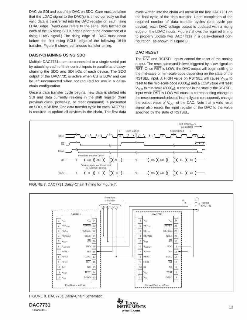
The remaining data transfer mode accepted by the DAC7731is continuous transfer. The CS of the DAC7731 can be tiedLOW or held LOW by the controller for an indefinite number ofserial clock cycles. Each clock cycle will transfer data into the
16-Bit Data Word
Most Significant Byte Least Significant Byte
Byte 1, Word N Byte 2, Word N
Byte 1, Word N – 1 Byte 2, Word N – 1
B15
A15 A14 A13 A8 A7 A6 A0
B14 B13 B8 B7 B6 B0
1 2 8 9 10 16
CS
SCLK
SDI
SDO
LDAC
1 2 16 1 2 16 1 2
B15 B14 B1 B0 C15 C14 C1 C0 D15 D14
C14C15B0B1B14B15A0A1A14A15
Word N Word N + 1 Word N + 2
Word N – 1 Word N Word N + 1
CS
SCLK
SDI
SDO
LDAC
FIGURE 6. Continuous Transfer Control.
FIGURE 5. Byte-Wide Data Write Cycle.
DAC7731 13SBAS249B www.ti.com
VCC
REFOUT
REFIN
REFADJ
VREF
ROFFSET
AGND
RFB2
RFB1
SJ
VOUT
VDD
VSS
REFEN
RSTSEL
SCLK
CS
SDO
SDI
LDAC
RST
NC
TEST
DGND
1
2
3
4
5
6
7
8
9
10
11
12
24
23
22
21
20
19
18
17
16
15
14
13
DAC7731
VCC
REFOUT
REFIN
REFADJ
VREF
ROFFSET
AGND
RFB2
RFB1
SJ
VOUT
VDD
VSS
REFEN
RSTSEL
SCLK
CS
SDO
SDI
LDAC
RST
NC
TEST
DGND
1
2
3
4
5
6
7
8
9
10
11
12
24
23
22
21
20
19
18
17
16
15
14
13
DAC7731
From HostController
To nextDAC7731
First Device in Chain Second Device in Chain
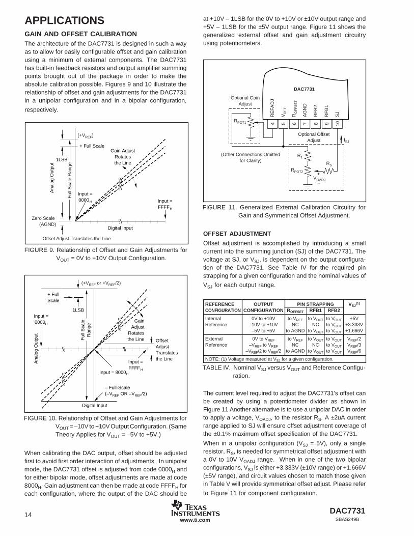
cycle written into the chain will arrive at the last DAC7731 onthe final cycle of the data transfer. Upon completion of therequired number of data transfer cycles (one cycle perdevice), each DAC voltage output is updated with a risingedge on the LDAC inputs. Figure 7 shows the required timingto properly update two DAC7731s in a daisy-chained con-figuration, as shown in Figure 8.
DAC RESET
The RST and RSTSEL inputs control the reset of the analogoutput. The reset command is level triggered by a low signal onRST. Once RST is LOW, the DAC output will begin settling tothe mid-scale or min-scale code depending on the state of theRSTSEL input. A HIGH value on RSTSEL will cause VOUT toreset to the mid-scale code (8000H) and a LOW value will resetVOUT to min-scale (8000H). A change in the state of the RSTSELinput while RST is LOW will cause a corresponding change inthe reset command selected internally and consequently changethe output value of VOUT of the DAC. Note that a valid resetsignal also resets the input register of the DAC to the valuespecified by the state of RSTSEL.
SCLK
CS
LDAC
SDI A15 A14 A0
X X XSDO
1 2 1 216 16
LSBs latched LSBs latched
Both DAC VOUT'sare updated
First Data Transfer Cycle
Previous cycle word from host(to DAC7731 B SDI)
B15 B14 B1 B0
A15 A14 A1 A0
FIGURE 7. DAC7731 Daisy-Chain Timing for Figure 7.
DAC via SDI and out of the DAC on SDO. Care must be takenthat the LDAC signal to the DAC(s) is timed correctly so thatvalid data is transferred into the DAC register on each risingLDAC edge. (Valid data refers to the serial data latched oneach of the 16 rising SCLK edges prior to the occurrence of arising LDAC signal.) The rising edge of LDAC must occurbefore the first rising SCLK edge of the following 16-bittransfer. Figure 6 shows continuous transfer timing.
DAISY-CHAINING USING SDO
Multiple DAC7731s can be connected to a single serial portby attaching each of their control inputs in parallel and daisy-chaining the SDO and SDI I/Os of each device. The SDOoutput of the DAC7731 is active when CS is LOW and canbe left unconnected when not required for use in a daisy-chain configuration.
Once a data transfer cycle begins, new data is shifted intoSDI and data currently residing in the shift register (fromprevious cycle, power-up, or reset command) is presentedon SDO, MSB first. One data transfer cycle for each DAC7731is required to update all devices in the chain. The first data
FIGURE 8. DAC7731 Daisy-Chain Schematic.
DAC773114SBAS249Bwww.ti.com
REFERENCE OUTPUT PIN STRAPPING VSJ(1)
CONFIGURATION CONFIGURATION ROFFSET RFB1 RFB2
Internal 0V to +10V to VREF to VOUT to VOUT +5VReference –10V to +10V NC NC to VOUT +3.333V
–5V to +5V to AGND to VOUT to VOUT +1.666V
External 0V to VREF to VREF to VOUT to VOUT VREF/2Reference –VREF to VREF NC NC to VOUT VREF/3
–VREF/2 to VREF/2 to AGND to VOUT to VOUT VREF/6
NOTE: (1) Voltage measured at VSJ for a given configuration.
APPLICATIONSGAIN AND OFFSET CALIBRATIONThe architecture of the DAC7731 is designed in such a wayas to allow for easily configurable offset and gain calibrationusing a minimum of external components. The DAC7731has built-in feedback resistors and output amplifier summingpoints brought out of the package in order to make theabsolute calibration possible. Figures 9 and 10 illustrate therelationship of offset and gain adjustments for the DAC7731in a unipolar configuration and in a bipolar configuration,
respectively.
at +10V – 1LSB for the 0V to +10V or ±10V output range and+5V – 1LSB for the ±5V output range. Figure 11 shows thegeneralized external offset and gain adjustment circuitryusing potentiometers.
FIGURE 9. Relationship of Offset and Gain Adjustments forVOUT = 0V to +10V Output Configuration.
Digital Input
H
Input =FFFF
H
Input =0000
Gain AdjustRotatesthe Line
1LSB
+ Full Scale
Ful
l Sca
le R
ange
Ana
log
Out
put
(+VREF)
Zero Scale (AGND)
Offset Adjust Translates the Line
FIGURE 10. Relationship of Offset and Gain Adjustments forVOUT = –10V to +10V Output Configuration. (SameTheory Applies for VOUT = –5V to +5V.)
Digital Input
Input =0000H
GainAdjust
Rotatesthe Line
1LSB
Ful
l Sca
leR
ange
+ FullScale
– Full-Scale(–VREF OR –VREF/2)
OffsetAdjustTranslatesthe Line
H
Input =FFFF
Input = 8000H
Ana
log
Out
put
(+VREF or +VREF/2)
When calibrating the DAC output, offset should be adjustedfirst to avoid first order interaction of adjustments. In unipolarmode, the DAC7731 offset is adjusted from code 0000H andfor either bipolar mode, offset adjustments are made at code8000H. Gain adjustment can then be made at code FFFFH foreach configuration, where the output of the DAC should be
Offset adjustment is accomplished by introducing a smallcurrent into the summing junction (SJ) of the DAC7731. Thevoltage at SJ, or VSJ, is dependent on the output configura-tion of the DAC7731. See Table IV for the required pinstrapping for a given configuration and the nominal values of
VSJ for each output range.
TABLE IV. Nominal VSJ versus VOUT and Reference Configu-ration.
The current level required to adjust the DAC7731’s offset canbe created by using a potentiometer divider as shown inFigure 11 Another alternative is to use a unipolar DAC in orderto apply a voltage, VOADJ, to the resistor RS. A ±2uA currentrange applied to SJ will ensure offset adjustment coverage ofthe ±0.1% maximum offset specification of the DAC7731.
When in a unipolar configuration (VSJ = 5V), only a singleresistor, RS, is needed for symmetrical offset adjustment witha 0V to 10V VOADJ range. When in one of the two bipolarconfigurations, VSJ is either +3.333V (±10V range) or +1.666V(±5V range), and circuit values chosen to match those givenin Table V will provide symmetrical offset adjust. Please refer
to Figure 11 for component configuration.
DAC7731 15SBAS249B www.ti.com
VCC
REFOUT
REFIN
REFADJ
VREF
ROFFSET
AGND
RFB2
RFB1
SJ
VOUT
VDD
VSS
REFEN
RSTSEL
SCLK
CS
SDO
SDI
LDAC
RST
NC
TEST
DGND
1
2
3
4
5
6
7
8
9
10
11
12
24
23
22
21
20
19
18
17
16
15
14
13
DAC7731
100kΩ1.0µF
(Other connections omitted for clarity.)
Low-Pass Reference Filter
FIGURE 14. Filtering the Internal Reference.
Figure 12 illustrates the typical minimum offset adjustmentranges provided by forcing a current at SJ for a given outputvoltage configuration.
OUTPUT RPOT2 R1 RS ISJ NOMINALCONFIGURATION RANGE OFFSET
ADJUSTMENT
0V to +10V 10K 0 2.5M ±2µA ±25mV–10V to +10V 10K 5K 1.5M ±2.2µA ±55mV–5V to +5V 10K 20K 1M ±1.7µA ±21mV
FIGURE 12. Offset Adjustment Transfer Characteristic.
GAIN ADJUSTMENTWhen using the internal reference of the DAC7731, gainadjustment is performed by adjusting the device’s internalreference voltage via the reference adjust pin, REFADJ. Theeffect of a reference voltage change on the gain of the DACoutput can be seen in the generic equation (for unipolarconfiguration):
VOUT = VREFIN • (N/65536)
Where N is represented in decimal format and ranges from0 to 65535.
REFADJ can be driven by a low impedance voltage sourcesuch as a unipolar, 0V to +10V DAC or a potentiometer (lessthan 100kΩ), see Figure 11. Since the input impedance ofREFADJ is typically 50kΩ, the smaller the resistance of thepotentiometer, the more linear the adjustment will be. A 10kΩpotentiometer is suggested if linearity of the reference adjust-ment is of concern.
When the DAC7731’s internal reference is not used, gainadjustments can be made via trimming the external refer-ence applied to the DAC at REFIN. This can be accomplishedthrough using a potentiometer, unipolar DAC, or other meansof precision voltage adjustment to control the voltage pre-sented to the DAC7731 by the external reference. Figure 13and Table VI summarize the range of adjustment of theinternal reference via REFADJ.
REFOUT ADJUST RANGE40
30
20
10
0
–10
–20
–30
–40
RE
FO
UT A
djus
tmen
t (m
V)
0 2 4 6 8 10
REFADJ (V)
Typical REFOUTAdjustment Range
Minimum REFOUTAdjustment Range
FIGURE 13. Internal Reference Adjustment Transfer Charac-teristic.
TABLE VI. Minimum Internal Reference Adjustment Range.
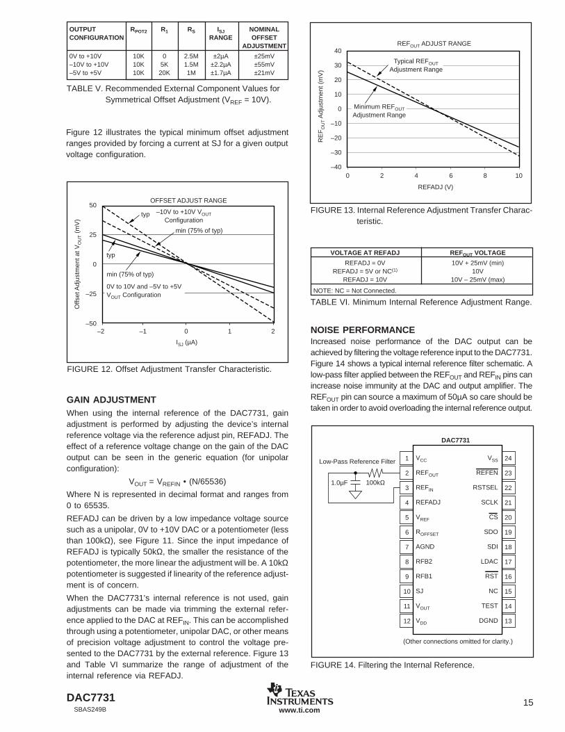
NOISE PERFORMANCEIncreased noise performance of the DAC output can beachieved by filtering the voltage reference input to the DAC7731.Figure 14 shows a typical internal reference filter schematic. Alow-pass filter applied between the REFOUT and REFIN pins canincrease noise immunity at the DAC and output amplifier. TheREFOUT pin can source a maximum of 50µA so care should betaken in order to avoid overloading the internal reference output.
DAC773116SBAS249Bwww.ti.com
LAYOUTA precision analog component requires careful layout, adequatebypassing, and clean, well-regulated power supplies. TheDAC7731 offers separate digital and analog supplies, as it willoften be used in close proximity with digital logic, microcontrollers,microprocessors, and digital signal processors. The more digitallogic present in the design and the higher the switching speed,the more important it will become to separate the analog anddigital ground and supply planes at the device.
Since the DAC7731 has both analog and digital ground pins,return currents can be better controlled and have less effecton the DAC output error. Ideally, AGND would be connecteddirectly to an analog ground plane and DGND to the digitalground plane. The analog ground plane would be separatefrom the ground connection for the digital components untilthey were connected at the power-entry point of the system.
The voltages applied to VCC and VSS should be well regulatedand low noise. Switching power supplies and DC/DC convert-ers will often have high-frequency glitches or spikes riding onthe output voltage. In addition, digital components can createsimilar high-frequency spikes as their internal logic switchesstates. This noise can easily couple into the DAC outputvoltage through various paths between the power connec-tions and analog output.
In addition, a 1µF to 10µF bypass capacitor in parallel with a0.1µF bypass capacitor is strongly recommended for eachsupply input. In some situations, additional bypassing may berequired, such as a 100µF electrolytic capacitor or even a Pifilter made up of inductors and capacitors–all designed toessentially low-pass filter the analog supplies, removing anyhigh frequency noise components.
PACKAGE OPTION ADDENDUM
www.ti.com 10-Jun-2014
Addendum-Page 1
PACKAGING INFORMATION
Orderable Device Status(1)
Package Type PackageDrawing
Pins PackageQty
Eco Plan(2)
Lead/Ball Finish(6)
MSL Peak Temp(3)
Op Temp (°C) Device Marking(4/5)
Samples
DAC7731E ACTIVE SSOP DB 24 60 Green (RoHS& no Sb/Br)
CU NIPDAU Level-3-260C-168 HR -40 to 85 DAC7731E
DAC7731E/1K ACTIVE SSOP DB 24 1000 Green (RoHS& no Sb/Br)
CU NIPDAU Level-3-260C-168 HR -40 to 85 DAC7731E
DAC7731EB ACTIVE SSOP DB 24 60 Green (RoHS& no Sb/Br)
CU NIPDAU Level-3-260C-168 HR -40 to 85 DAC7731EB
DAC7731EB/1K ACTIVE SSOP DB 24 1000 Green (RoHS& no Sb/Br)
CU NIPDAU Level-3-260C-168 HR -40 to 85 DAC7731EB
DAC7731EB/1KG4 ACTIVE SSOP DB 24 1000 Green (RoHS& no Sb/Br)
CU NIPDAU Level-3-260C-168 HR -40 to 85 DAC7731EB
DAC7731EBG4 ACTIVE SSOP DB 24 60 Green (RoHS& no Sb/Br)
CU NIPDAU Level-3-260C-168 HR -40 to 85 DAC7731EB
DAC7731EC ACTIVE SSOP DB 24 60 Green (RoHS& no Sb/Br)
CU NIPDAU Level-3-260C-168 HR -40 to 85 DAC7731EC
DAC7731EC/1K ACTIVE SSOP DB 24 1000 Green (RoHS& no Sb/Br)
CU NIPDAU Level-3-260C-168 HR -40 to 85 DAC7731EC
DAC7731ECG4 ACTIVE SSOP DB 24 60 Green (RoHS& no Sb/Br)
CU NIPDAU Level-3-260C-168 HR -40 to 85 DAC7731EC
DAC7731EG4 ACTIVE SSOP DB 24 60 Green (RoHS& no Sb/Br)
CU NIPDAU Level-3-260C-168 HR -40 to 85 DAC7731E
(1) The marketing status values are defined as follows:ACTIVE: Product device recommended for new designs.LIFEBUY: TI has announced that the device will be discontinued, and a lifetime-buy period is in effect.NRND: Not recommended for new designs. Device is in production to support existing customers, but TI does not recommend using this part in a new design.PREVIEW: Device has been announced but is not in production. Samples may or may not be available.OBSOLETE: TI has discontinued the production of the device.
(2) Eco Plan - The planned eco-friendly classification: Pb-Free (RoHS), Pb-Free (RoHS Exempt), or Green (RoHS & no Sb/Br) - please check http://www.ti.com/productcontent for the latest availabilityinformation and additional product content details.TBD: The Pb-Free/Green conversion plan has not been defined.Pb-Free (RoHS): TI's terms "Lead-Free" or "Pb-Free" mean semiconductor products that are compatible with the current RoHS requirements for all 6 substances, including the requirement thatlead not exceed 0.1% by weight in homogeneous materials. Where designed to be soldered at high temperatures, TI Pb-Free products are suitable for use in specified lead-free processes.Pb-Free (RoHS Exempt): This component has a RoHS exemption for either 1) lead-based flip-chip solder bumps used between the die and package, or 2) lead-based die adhesive used betweenthe die and leadframe. The component is otherwise considered Pb-Free (RoHS compatible) as defined above.Green (RoHS & no Sb/Br): TI defines "Green" to mean Pb-Free (RoHS compatible), and free of Bromine (Br) and Antimony (Sb) based flame retardants (Br or Sb do not exceed 0.1% by weightin homogeneous material)
(3) MSL, Peak Temp. - The Moisture Sensitivity Level rating according to the JEDEC industry standard classifications, and peak solder temperature.
(4) There may be additional marking, which relates to the logo, the lot trace code information, or the environmental category on the device.
(5) Multiple Device Markings will be inside parentheses. Only one Device Marking contained in parentheses and separated by a "~" will appear on a device. If a line is indented then it is a continuationof the previous line and the two combined represent the entire Device Marking for that device.
(6) Lead/Ball Finish - Orderable Devices may have multiple material finish options. Finish options are separated by a vertical ruled line. Lead/Ball Finish values may wrap to two lines if the finishvalue exceeds the maximum column width.
Important Information and Disclaimer:The information provided on this page represents TI's knowledge and belief as of the date that it is provided. TI bases its knowledge and belief on informationprovided by third parties, and makes no representation or warranty as to the accuracy of such information. Efforts are underway to better integrate information from third parties. TI has taken andcontinues to take reasonable steps to provide representative and accurate information but may not have conducted destructive testing or chemical analysis on incoming materials and chemicals.TI and TI suppliers consider certain information to be proprietary, and thus CAS numbers and other limited information may not be available for release.
In no event shall TI's liability arising out of such information exceed the total purchase price of the TI part(s) at issue in this document sold by TI to Customer on an annual basis.
NOTES: A. All linear dimensions are in millimeters.B. This drawing is subject to change without notice.C. Body dimensions do not include mold flash or protrusion not to exceed 0,15.D. Falls within JEDEC MO-150
IMPORTANT NOTICETexas Instruments Incorporated and its subsidiaries (TI) reserve the right to make corrections, enhancements, improvements and otherchanges to its semiconductor products and services per JESD46, latest issue, and to discontinue any product or service per JESD48, latestissue. Buyers should obtain the latest relevant information before placing orders and should verify that such information is current andcomplete. All semiconductor products (also referred to herein as “components”) are sold subject to TI’s terms and conditions of salesupplied at the time of order acknowledgment.TI warrants performance of its components to the specifications applicable at the time of sale, in accordance with the warranty in TI’s termsand conditions of sale of semiconductor products. Testing and other quality control techniques are used to the extent TI deems necessaryto support this warranty. Except where mandated by applicable law, testing of all parameters of each component is not necessarilyperformed.TI assumes no liability for applications assistance or the design of Buyers’ products. Buyers are responsible for their products andapplications using TI components. To minimize the risks associated with Buyers’ products and applications, Buyers should provideadequate design and operating safeguards.TI does not warrant or represent that any license, either express or implied, is granted under any patent right, copyright, mask work right, orother intellectual property right relating to any combination, machine, or process in which TI components or services are used. Informationpublished by TI regarding third-party products or services does not constitute a license to use such products or services or a warranty orendorsement thereof. Use of such information may require a license from a third party under the patents or other intellectual property of thethird party, or a license from TI under the patents or other intellectual property of TI.Reproduction of significant portions of TI information in TI data books or data sheets is permissible only if reproduction is without alterationand is accompanied by all associated warranties, conditions, limitations, and notices. TI is not responsible or liable for such altereddocumentation. Information of third parties may be subject to additional restrictions.Resale of TI components or services with statements different from or beyond the parameters stated by TI for that component or servicevoids all express and any implied warranties for the associated TI component or service and is an unfair and deceptive business practice.TI is not responsible or liable for any such statements.Buyer acknowledges and agrees that it is solely responsible for compliance with all legal, regulatory and safety-related requirementsconcerning its products, and any use of TI components in its applications, notwithstanding any applications-related information or supportthat may be provided by TI. Buyer represents and agrees that it has all the necessary expertise to create and implement safeguards whichanticipate dangerous consequences of failures, monitor failures and their consequences, lessen the likelihood of failures that might causeharm and take appropriate remedial actions. Buyer will fully indemnify TI and its representatives against any damages arising out of the useof any TI components in safety-critical applications.In some cases, TI components may be promoted specifically to facilitate safety-related applications. With such components, TI’s goal is tohelp enable customers to design and create their own end-product solutions that meet applicable functional safety standards andrequirements. Nonetheless, such components are subject to these terms.No TI components are authorized for use in FDA Class III (or similar life-critical medical equipment) unless authorized officers of the partieshave executed a special agreement specifically governing such use.Only those TI components which TI has specifically designated as military grade or “enhanced plastic” are designed and intended for use inmilitary/aerospace applications or environments. Buyer acknowledges and agrees that any military or aerospace use of TI componentswhich have not been so designated is solely at the Buyer's risk, and that Buyer is solely responsible for compliance with all legal andregulatory requirements in connection with such use.TI has specifically designated certain components as meeting ISO/TS16949 requirements, mainly for automotive use. In any case of use ofnon-designated products, TI will not be responsible for any failure to meet ISO/TS16949.Products ApplicationsAudio www.ti.com/audio Automotive and Transportation www.ti.com/automotiveAmplifiers amplifier.ti.com Communications and Telecom www.ti.com/communicationsData Converters dataconverter.ti.com Computers and Peripherals www.ti.com/computersDLP® Products www.dlp.com Consumer Electronics www.ti.com/consumer-appsDSP dsp.ti.com Energy and Lighting www.ti.com/energyClocks and Timers www.ti.com/clocks Industrial www.ti.com/industrialInterface interface.ti.com Medical www.ti.com/medicalLogic logic.ti.com Security www.ti.com/securityPower Mgmt power.ti.com Space, Avionics and Defense www.ti.com/space-avionics-defenseMicrocontrollers microcontroller.ti.com Video and Imaging www.ti.com/videoRFID www.ti-rfid.comOMAP Applications Processors www.ti.com/omap TI E2E Community e2e.ti.comWireless Connectivity www.ti.com/wirelessconnectivity