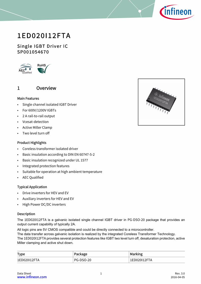
Data Sheet 1 Rev. 3.0 www.infineon.com 2016-04-05 1ED020I12FTA Single IGBT Driver IC SP001054670 1 Overview Main Features • Single channel isolated IGBT Driver • For 600V/1200V IGBTs • 2 A rail-to-rail output • Vcesat-detection • Active Miller Clamp • Two level turn off Product Highlights • Coreless transformer isolated driver • Basic insulation according to DIN EN 60747-5-2 • Basic insulation recognized under UL 1577 • Integrated protection features • Suitable for operation at high ambient temperature • AEC Qualified Typical Application • Drive inverters for HEV and EV • Auxiliary inverters for HEV and EV • High Power DC/DC inverters Description The 1ED020I12FTA is a galvanic isolated single channel IGBT driver in PG-DSO-20 package that provides an output current capability of typically 2A. All logic pins are 5V CMOS compatible and could be directly connected to a microcontroller. The data transfer across galvanic isolation is realized by the integrated Coreless Transformer Technology. The 1ED020I12FTA provides several protection features like IGBT two level turn off, desaturation protection, active Miller clamping and active shut down. Type Package Marking 1ED020I12FTA PG-DSO-20 1ED020I12FTA
Transcript
Data Sheet 1 Rev. 3.0www.infineon.com 2016-04-05
1ED020I12FTASingle IGBT Driver ICSP001054670
1 Overview
Main Features
• Single channel isolated IGBT Driver • For 600V/1200V IGBTs• 2 A rail-to-rail output• Vcesat-detection• Active Miller Clamp• Two level turn off
Product Highlights
• Coreless transformer isolated driver• Basic insulation according to DIN EN 60747-5-2• Basic insulation recognized under UL 1577• Integrated protection features• Suitable for operation at high ambient temperature• AEC Qualified
Typical Application
• Drive inverters for HEV and EV• Auxiliary inverters for HEV and EV• High Power DC/DC inverters
Description
The 1ED020I12FTA is a galvanic isolated single channel IGBT driver in PG-DSO-20 package that provides anoutput current capability of typically 2A.All logic pins are 5V CMOS compatible and could be directly connected to a microcontroller.The data transfer across galvanic isolation is realized by the integrated Coreless Transformer Technology.The 1ED020I12FTA provides several protection features like IGBT two level turn off, desaturation protection, activeMiller clamping and active shut down.
IN+ control signal for the driver output if IN- is set to low. (The IGBT is on if IN+ = high and IN- = low)A minimum pulse width is defined to make the IC robust against glitches at IN+. An internal Pull-Down-Resistorensures IGBT Off-State.
IN- Inverting Driver Input
IN- control signal for driver output if IN+ is set to high. (IGBT is on if IN- = low and IN+ = high)A minimum pulse width is defined to make the IC robust against glitches at IN-. An internal Pull-Up-Resistorensures IGBT Off-State.
/RST Reset Input
Function 1: Enable/shutdown of the input chip. (The IGBT is off if /RST = low). A minimum pulse width isdefined to make the IC robust against glitches at /RST.Function 2: Resets the DESAT-FAULT-state of the chip if /RST is low for a time TRST. An internal Pull-Up-Resistoris used to ensure /FLT status output.
/FLT Fault Output
Open-drain output to report a desaturation error of the IGBT (FLT is low if desaturation occurs)
RDY Ready Status
Open-drain output to report the correct operation of the device (RDY = high if both chips are above the UVLOlevel and the internal chip transmission is faultless).
VEE2
IN+
IN-
RDY
/RST
/FLT
VCC1
GND1
VCC2
OUT
GND2
CLAMP
DESAT
TLSET
VEE2
GND1VEE2
1
2
3
4
5
9
20
19
18
17
16
15
14
13
1211
GND1
GND1
10
7
8
6
VEE2
1ED020I12FTASingle IGBT Driver IC
Pin Configuration and Functionality
Data Sheet 9 Rev. 3.0 2016-04-05
VCC1
5 V power supply of the input chip
VEE2
Negative power supply pins of the output chip. If no negative supply voltage is available, all VEE2 pins have tobe connected to GND2.
DESAT Desaturation Detection Input
Monitoring of the IGBT saturation voltage (VCE) to detect desaturation caused by short circuits. If OUT is high,VCE is above a defined value and a certain blanking time has expired, the desaturation protection is activatedand the IGBT is switched off. The blanking time is adjustable by an external capacitor.
CLAMP Miller Clamping
Ties the gate voltage to ground after the IGBT has been switched off at a defined voltage to avoid a parasiticswitch-on of the IGBT.During turn-off, the gate voltage is monitored and the clamp output is activated whenthe gate voltage goes below 2 V below VEE2.
GND2 Reference Ground
Reference ground of the output chip.
OUT Driver Output
Output pin to drive an IGBT. The voltage is switched between VEE2 and VCC2. In normal operating mode Voutis controlled by IN+, IN- and /RST. During error mode (UVLO, internal error or DESAT) Vout is set to VEE2independent of the input control signals.
VCC2
Positive power supply pin of the output side.
TLSET Two Level Turn Off Adjust
Circuitry at TLSET adjust the two level turn off time with an external capacitor to GND2 and the two levelvoltage with an external Zener diode to GND2, for wave forms please see Figure 7-4.
1ED020I12FTASingle IGBT Driver IC
Functional Description
Data Sheet 10 Rev. 3.0 2016-04-05
4 Functional Description
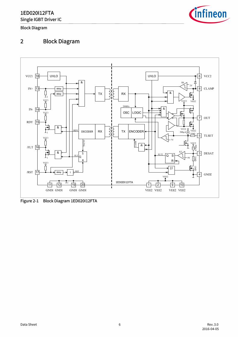
4.1 IntroductionThe 1ED020I12FTA is an advanced IGBT gate driver for motor drives typical greater 10 kW. Control andprotection functions are included to make possible the design of high reliability systems.The device consists of two galvanic separated parts. The input chip can be directly connected to a standard5 V DSP or microcontroller with CMOS in/output and the output chip is connected to the high voltage side.An effective active Miller clamp function avoids the need of negative gate driving in some applications andallows the use of a simple bootstrap supply for the high side driver.A rail-to-rail driver output enables the user to provide easy clamping of the IGBTs gate voltage during shortcircuit of the IGBT. So an increase of short circuit current due to the feedback via the Miller capacitance can beavoided. Further, a rail-to-rail output reduces power dissipation.The device also includes an IGBT desaturation protection with a FAULT status output.A two-level turn-off feature with adjustable delay protects against excessive overvoltage at turn-off in case ofovercurrent or short circuit condition. The same delay is applied at turn-on to prevent pulse width distortion.A READY status output reports if the device is supplied and operates correctly.
Figure 4-1 Application Example Bipolar Supply
4.2 SupplyThe driver 1ED020I12FTA is designed to support two different supply configurations, bipolar supply andunipolar supply.In bipolar supply the driver is typically supplied with a positive voltage of 15V at VCC2 and a negative voltageof -8V at VEE2, refer to Figure 4-1. Negative supply prevents a dynamic turn on due to the additional chargewhich is generated from IGBT input capacitance times negative supply voltage. If an appropriate negativesupply voltage is used, connecting CLAMPxx to IGBT gate is redundant and therefore typically not necessary.For unipolar supply configuration the driver is typically supplied with a positive voltage of 15V at VCC2.Erratically dynamic turn on of the IGBT could be prevented with active Miller clamp function, so CLAMP outputis directly connected to IGBT gate, refer to Figure 4-2.
GND1
IN+
IN-
RDY
/FLT
/RST
VCC1
OUT
VCC2
GND2
CLAMP
1ED020I12FTA
DESAT
+5V
VEE2
SGND
IN+
RDY
FLT
RST
+15V
-8V
TLSET
10R
1k10k
10k
10R
220p47p10V
1µ
1µ
100n
1ED020I12FTASingle IGBT Driver IC
Functional Description
Data Sheet 11 Rev. 3.0 2016-04-05
Figure 4-2 Application Example Unipolar Supply
4.3 Internal Protection Features
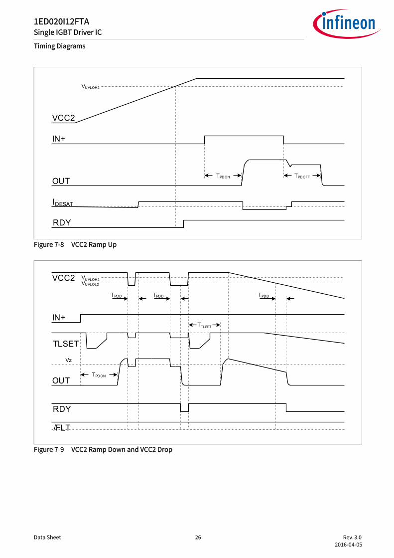
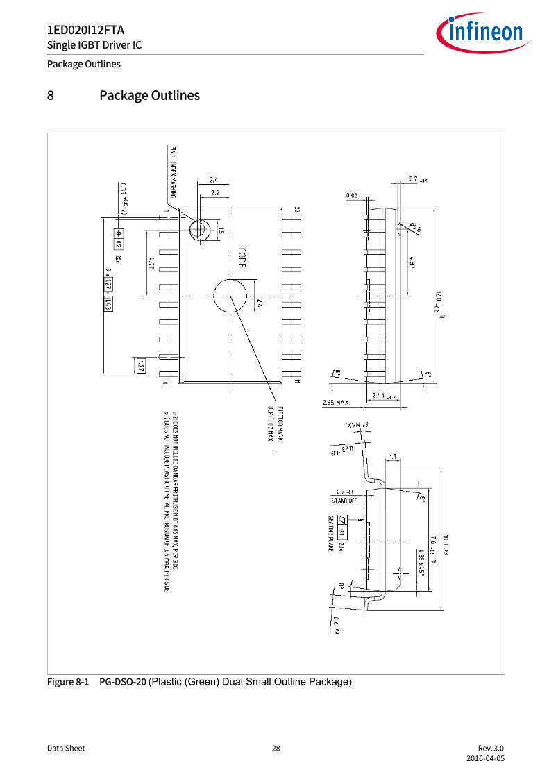
4.3.1 Undervoltage Lockout (UVLO)To ensure correct switching of IGBTs the device is equipped with an undervoltage lockout for both chips, referto Figure 7-8 and Figure 7-9.If the power supply voltage VVCC1 of the input chip drops below VUVLOL1 a turn-off signal is sent to the outputchip before power-down. The IGBT is switched off and the signals at IN+ and IN- are ignored as long as VVCC1reaches the power-up voltage VUVLOH1.If the power supply voltage VVCC2 of the output chip goes down below VUVLOL2 the IGBT is switched off andsignals from the input chip are ignored as long as VVCC2 reaches the power-up voltage VUVLOH2. VEE2 is notmonitored, otherwise negative supply voltage range from 0 V to -12 V would not be possible.
4.3.2 READY Status OutputThe READY output at pin /RDY shows the status of three internal protection features.• UVLO of the input chip• UVLO of the output chip after a short delay• Internal signal transmission after a short delayIt is not necessary to reset the READY signal since its state only depends on the status of the former mentionedprotection signals.
4.3.3 Watchdog TimerDuring normal operation the internal signal transmission is monitored by a watchdog timer. If thetransmission fails for a given time, the IGBT is switched off and the READY output reports an internal error.
4.3.4 Active Shut-DownThe Active Shut-Down feature ensures a safe IGBT off-state if the output chip is not connected to the powersupply, IGBT gate is clamped at OUT to VEE2.
GND1
IN+
IN-
RDY
/FLT
/RST
VCC1
OUT
VCC2
GND2
CLAMP
1ED020I12FTA
DESAT
+5V
VEE2
SGND
IN+
RDY
FLT
RST
+15V
TLSET
10R
1k10k
10k
10R
220p47p10V
1µ100n
1ED020I12FTASingle IGBT Driver IC
Functional Description
Data Sheet 12 Rev. 3.0 2016-04-05
4.4 Non-Inverting and Inverting InputsThere are two possible input modes to control the IGBT. At non-inverting mode IN+ controls the driver outputwhile IN- is set to low. At inverting mode IN- controls the driver output while IN+ is set to high, refer toFigure 7-2. A minimum input pulse width is defined to filter occasional glitches.
4.5 Driver OutputThe output driver section uses only MOSFETs to provide a rail-to-rail output. This feature permits that tightcontrol of gate voltage during on-state and short circuit can be maintained as long as the drivers supply isstable. Due to the low internal voltage drop, switching behaviour of the IGBT is predominantly governed bythe gate resistor. Furthermore, it reduces the power to be dissipated by the driver.
4.6 Two-Level Turn-OffThe Two-Level Turn-OFF introduces a second turn off voltage level at the driver output in between ON- andOFF-level, refer to Figure 7-3. This additional level ensures lower VCE overshoots at turn off by reducing gateemitter voltage of the IGBT at short circuits or over current events. The VGE level is adjusting the current of theIGBT at the end two level turn off interval, the required timing is depending on stray inductance and overcurrent at beginning of two level turn off interval.Reference voltage level and hold up time could be adjusted at TLSET pin. The reference voltage is set by therequired Zener diode connected between pin TLSET and GND2. The holdup time is set by the capacitorconnected to the same pin TLSET and GND2.The hold time can be adjusted during switch on using the whole capacitance connected at pin TLSET includingcapacitor, parasitic wiring capacitance and junction capacitance of Zener diode. When a switch on signal isgiven the IC starts to discharge CTLSET. Discharging CTLSET is stopped after 500 ns. Then Ctlset is charged withan internal charge current ITLSET. When the voltage of the capacitor CTLSET exceeds 7 V a second current sourcestarts charging CTLSET up to VZDIODE. At the end of this discharge-charge cycle the gate driver is switched on.The time between IN initiated switch-on signal (minus an internal propagation delay of approximately 200 ns)and switch-on of the gate drive is sampled and stored digitally. It represents the two level turn off set timeTTLSET during switch-off. Due to digitalization the tpdon time can vary in time steps of 50 ns.If switch off is initiated from IN+, IN- or /RST signal, the gate driver is switched off immediately after internalpropagation delay of approximately 200 ns and VOUT begins to decrease to the second gate voltage level. For switch off initiated by DESAT, the gate driver switch off is delayed by desaturation sense to OUT delay,afterwards VOUT begins to decrease to the second gate voltage level. For reaching second gate voltage level the output voltage VOUT is sensed and compared with the Zener voltageVZDIODE. When VOUT falls below the reference voltage VZDIODE of the Zener diode the switch off process isinterrupted and VOUT is adjusted to VZDIODE. OUT is switched to VEE2 after the holdup time has passed.The Two-Level Turn-OFF function cannot be disabled.
1ED020I12FTASingle IGBT Driver IC
Functional Description
Data Sheet 13 Rev. 3.0 2016-04-05
4.7 Minimal On Time / Off TimeThe 1ED020I12FTA driver requires minimal on and off time for proper operation in the application. Minimal ontime must be greater than the adjustable two level plateau time TTLSET, shorter on times will be suppressed bygenerating of the plateau time refer to Figure 7-5. Due to the short on time, the voltage at TLSET pin does notreach the comparator threshold; therefore the driver does not turn on. A similar principle takes place for offtime. Minimal off time must be greater than TTLSET; shorter off times will be suppressed, which means OUTstays on refer to Figure 7-6. A two level turn off plateau cannot be shortened by the driver. If the driver hasentered the turn off sequence it cannot switch off due to the fact, that the driver has already entered the shutoff mode. But if the driver input signal is turned on again, it will leave the lower level after TTLSET time byswitching OUT to high, refer to Figure 7-7.
4.8 External Protection Features
4.8.1 Desaturation ProtectionA desaturation protection ensures the protection of the IGBT at short circuit. When the DESAT voltage goes upand reaches 9 V, the output is driven low, refer to Figure 7-4. Further, the FAULT output is activated. Aprogrammable blanking time is used to allow enough time for IGBT saturation. Blanking time is provided by ahighly precise internal current source and an external capacitor.
4.8.2 Active Miller ClampIn a half bridge configuration the switched off IGBT tends to dynamically turn on during turn on phase of theopposite IGBT. A Miller clamp allows sinking the Miller current across a low impedance path in this high dV/dtsituation. Therefore in many applications, the use of a negative supply voltage can be avoided. During turn-off, the gate voltage is monitored and the clamp output is activated when the gate voltage goesbelow typical 2 V (related to VEE2). The clamp is designed for a Miller current up to 2 A.
4.8.3 Short Circuit ClampingDuring short circuit the IGBTs gate voltage tends to rise because of the feedback via the Miller capacitance. Anadditional protection circuit connected to OUT and CLAMP limits this voltage to a value slightly higher thanthe supply voltage. A current of maximum 500 mA for 10 μs may be fed back to the supply through one of thispaths. If higher currents are expected or a tighter clamping is desired external Schottky diodes may be added.
4.9 RESETThe reset input has two functions.Firstly, /RST is in charge of setting back the FAULT output. If /RST is low longer than a given time, /FLT will becleared at the rising edge of /RST, refer to Figure 7-4; otherwise, it will remain unchanged. Moreover, it worksas enable/shutdown of the input logic, refer to Figure 7-2.
1ED020I12FTASingle IGBT Driver IC
Electrical Parameters
Data Sheet 14 Rev. 3.0 2016-04-05
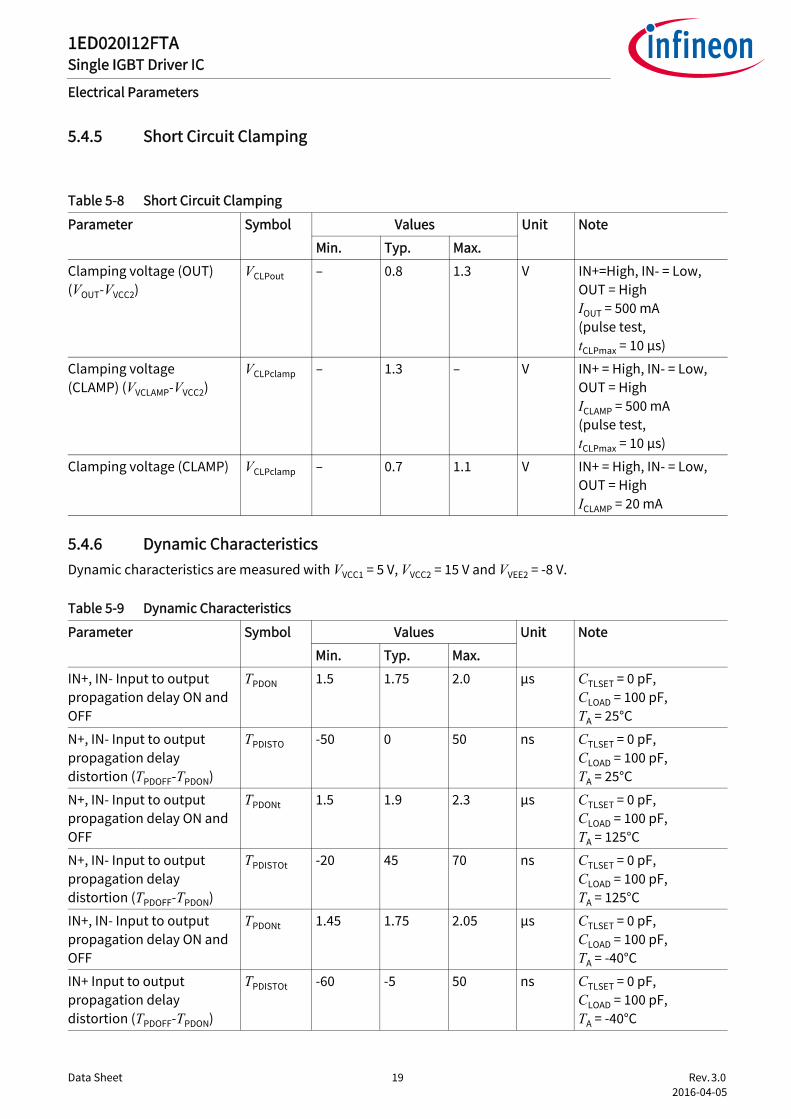
5 Electrical Parameters
5.1 Absolute Maximum Ratings
Note: Absolute maximum ratings are defined as ratings, which when being exceeded may lead to destruction of the integrated circuit. Unless otherwise noted all parameters refer to GND1.
Table 5-1 Absolute Maximum Ratings
Parameter Symbol Values Unit Note
Min. Max.
Positive power supply output side VVCC2 -0.3 20 V 1)
1) With respect to GND2.
Negative power supply output side VVEE2 -12 0.3 V 1)
Maximum power supply voltage output side(VVCC2 - VVEE2)
Vmax2 – 28 V –
Gate driver output VOUT VVEE2-0.3 VVCC2+0.3 V –
Gate driver high output maximum current IOUT – 2.4 A t = 2 µs
Gate & Clamp driver low output maximum current
IOUT – 2.4 A t = 2 µs
Maximum short circuit clamping time tCLP – 10 μs ICLAMP/OUT = 500 mA
Positive power supply input side VVCC1 -0.3 6.5 V –
Logic input voltages(IN+,IN-,RST)
VLogicIN -0.3 6.5 V –
Opendrain Logic output voltage (FLT) VFLT# -0.3 6.5 V –
Opendrain Logic output voltage (RDY) VRDY -0.3 6.5 V –
Opendrain Logic output current (FLT) IFLT# – 10 mA –
Opendrain Logic output current (RDY) IRDY – 10 mA –
Pin DESAT voltage VDESAT -0.3 VVCC2 +0.3 V 1)
Pin CLAMP voltage VCLAMP -0.3 VVCC2 +0.32)
2) May be exceeded during short circuit clamping.
V 3)
Junction temperature TJ -40 150 °C –
Storage temperature TS -55 150 °C –
Power dissipation, per input part PD, IN – 100 mW 4) @TA = 25°C
Power dissipation, per output part PD, OUT – 700 mW 4) @TA = 25°C
Note: Within the operating range the IC operates as described in the functional description. Unless otherwise noted all parameters refer to GND1.
5.3 Recommended Operating Parameters
Note: Unless otherwise noted all parameters refer to GND1.
3) With respect to VEE2.4) Output IC power dissipation is derated linearly at 8.5 mW/°C above 68°C. Input IC power dissipation does not require
derating. See Figure 9-1 for reference layouts for these thermal data. Thermal performance may change significantly with layout and heat dissipation of components in close proximity.
5) According to EIA/JESD22-A114-B (discharging a 100 pF capacitor through a 1.5 kΩ series resistor).
Table 5-2 Operating Parameters
Parameter Symbol Values Unit Note
Min. Max.
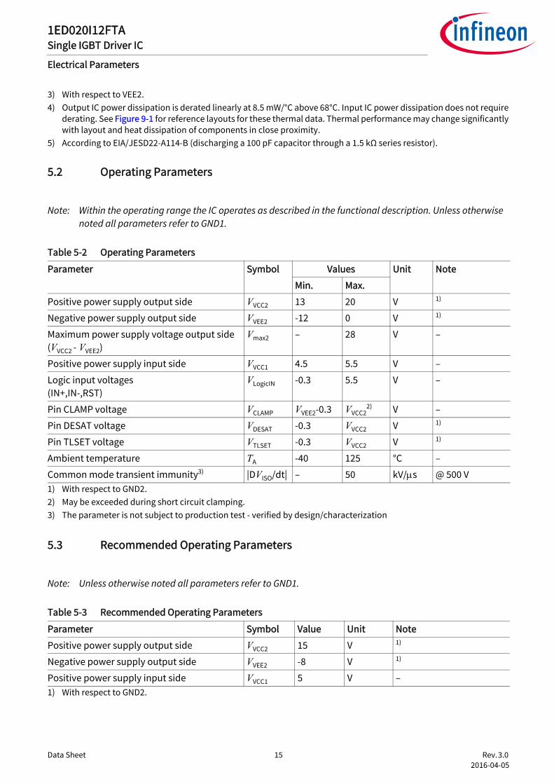
Positive power supply output side VVCC2 13 20 V 1)
1) With respect to GND2.
Negative power supply output side VVEE2 -12 0 V 1)
Maximum power supply voltage output side(VVCC2 - VVEE2)
Vmax2 – 28 V –
Positive power supply input side VVCC1 4.5 5.5 V –
Logic input voltages (IN+,IN-,RST)
VLogicIN -0.3 5.5 V –
Pin CLAMP voltage VCLAMP VVEE2-0.3 VVCC22)
2) May be exceeded during short circuit clamping.
V –
Pin DESAT voltage VDESAT -0.3 VVCC2 V 1)
Pin TLSET voltage VTLSET -0.3 VVCC2 V 1)
Ambient temperature TA -40 125 °C –
Common mode transient immunity3)
3) The parameter is not subject to production test - verified by design/characterization
|DVISO/dt| – 50 kV/μs @ 500 V
Table 5-3 Recommended Operating Parameters
Parameter Symbol Value Unit Note
Positive power supply output side VVCC2 15 V 1)
1) With respect to GND2.
Negative power supply output side VVEE2 -8 V 1)
Positive power supply input side VVCC1 5 V –
1ED020I12FTASingle IGBT Driver IC
Electrical Parameters
Data Sheet 16 Rev. 3.0 2016-04-05
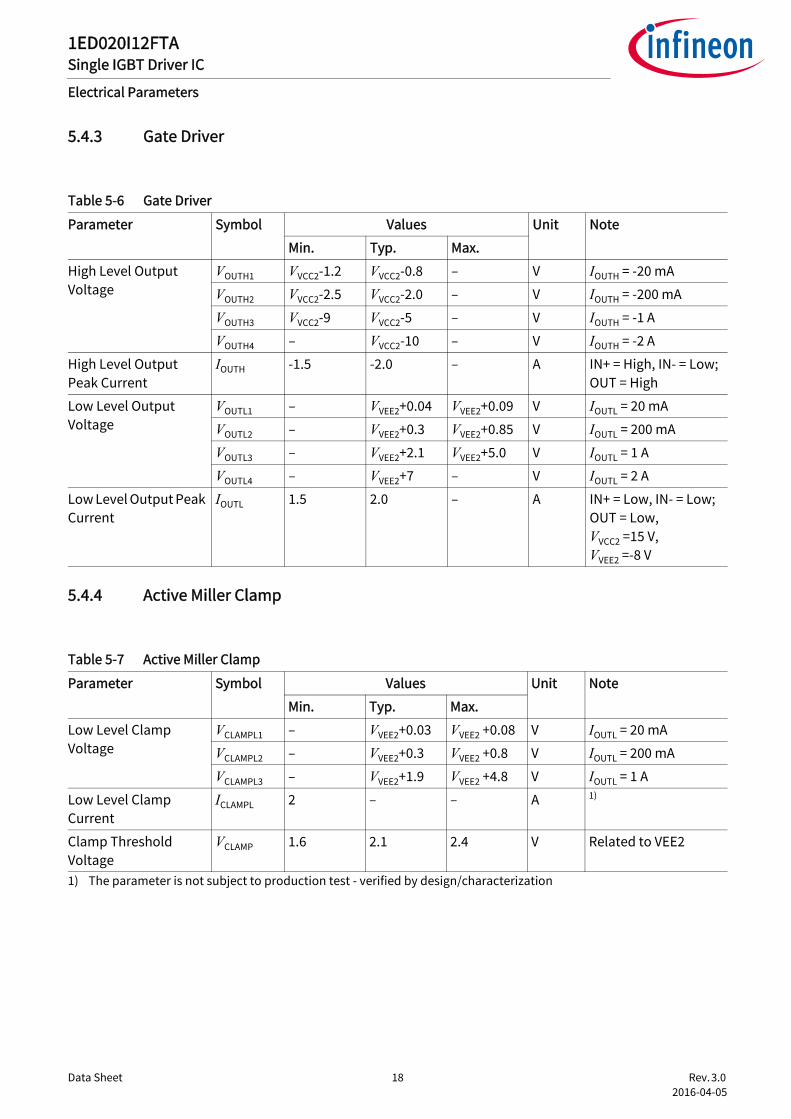
5.4 Electrical Characteristics
Note: The electrical characteristics include the spread of values in supply voltages, load and junction temperatures given below. Typical values represent the median values at TA = 25°C. Unless otherwise noted all voltages are given with respect to their respective GND (GND1 for pins 11 to 20, GND2 for pins 1 to 10).
5.4.1 Voltage Supply
Table 5-4 Voltage Supply
Parameter Symbol Values Unit Note
Min. Typ. Max.
UVLO Threshold Input Chip VUVLOH1 – 4.1 4.3 V –
VUVLOL1 3.5 3.8 – V –
UVLO Hysteresis Input Chip(VUVLOH1 - VUVLOL1)
VHYS1 0.15 – – V –
UVLO Threshold Output Chip VUVLOH2 – 12.0 12.6 V –
VUVLOL2 10.4 11.0 – V –
UVLO Hysteresis Output Chip(VUVLOH1 - VUVLOL1)
VHYS2 0.7 0.9 – V –
Quiescent Current Input Chip IQ1 – 7 9 mA VVCC1 =5 VIN+ = High,IN- = Low=>OUT = High,RDY = High,/FLT = High
Quiescent Current Output Chip
IQ2 – 4.5 6 mA VVCC2 =15 VVVEE2 =-8 VIN+ = High,IN- = Low=>OUT = High,RDY = High,/FLT = High
1ED020I12FTASingle IGBT Driver IC
Electrical Parameters
Data Sheet 17 Rev. 3.0 2016-04-05
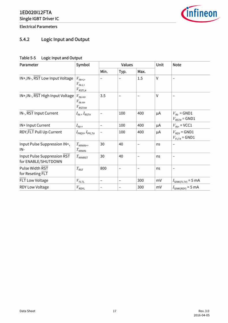
5.4.2 Logic Input and Output
Table 5-5 Logic Input and Output
Parameter Symbol Values Unit Note
Min. Typ. Max.
IN+,IN-, RST Low Input Voltage VIN+L,VIN-L,VRSTL#
– – 1.5 V –
IN+,IN-, RST High Input Voltage VIN+H,VIN-H,VRSTH#
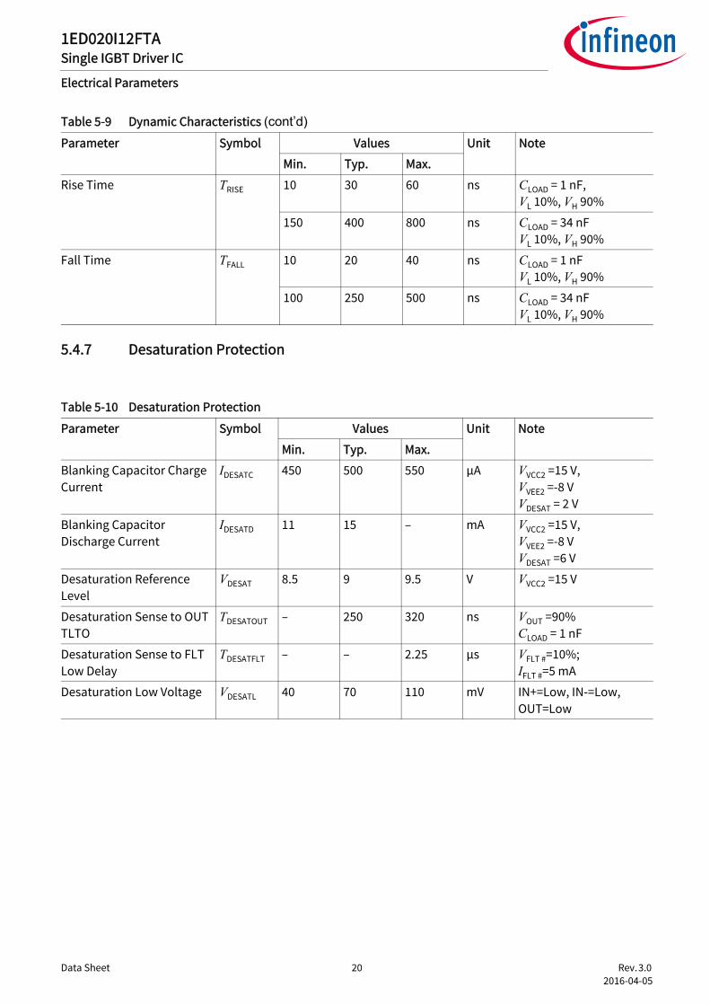
Table 5-9 Dynamic Characteristics (cont’d)Parameter Symbol Values Unit Note
Min. Typ. Max.
1ED020I12FTASingle IGBT Driver IC
Electrical Parameters
Data Sheet 21 Rev. 3.0 2016-04-05
5.4.8 Active Shut Down
5.4.9 Two-level Turn-off
Table 5-11 Active Shut Down
Parameter Symbol Values Unit Note
Min. Typ. Max.
Active Shut Down Voltage VACTSD1)
1) With reference to VEE2
– – 2.0 V IOUT = -200 mA,VCC2 open
Table 5-12 Two-level Turn-off
Parameter Symbol Values Unit Note
Min. Typ. Max.
External reference voltage range (Zener-Diode)
VZDIODE 7.5 – VCC2-0.5 V –
Reference Voltage for setting two-level delay time
VTLSET 6.6 7 7.3 V –
Current for setting two-level delay time and external reference voltage (Zener-Diode)
ITLSET 420 500 550 μA VTLSET = 10 V
External Capacitance Range CTLSET 0 – 220 pF –
1ED020I12FTASingle IGBT Driver IC
Insulation Characteristics
Data Sheet 22 Rev. 3.0 2016-04-05
6 Insulation CharacteristicsInsulation characteristics are guaranteed only within the safety maximum ratings which must be ensured byprotective circuits in application. Surface mount classification is class A in accordance with CECCOO802.This coupler is suitable for “basic insulation” only within the safety ratings. Compliance with the safety ratingsshall be ensured by means of suitable protective circuits.
6.1 Certified according to DIN EN 60747-5-2 (VDE 0884 Teil 2): 2003-01. Basic Insulation
6.2 Recognized under UL 1577
6.3 ReliabilityFor Qualification Report please contact your local Infineon Technologies office.
Table 6-1 Certified according to DIN EN 60747-5-2
Description Symbol Characteristic Unit
Installation classification per EN 60664-1, Table 1for rated mains voltage ≤ 150 VRMSfor rated mains voltage ≤ 300 VRMSfor rated mains voltage ≤ 600 VRMS
I-IVI-IIII-II
–
Climatic Classification 40/125/21 –
Pollution Degree (EN 60664-1) 2 –
Minimum External Clearance CLR 8 mm
Minimum External Creepage CPG 8 mm
Minimum Comparative Tracking Index CTI 175 –
Maximum Repetitive Insulation Voltage VIORM 1420 VPEAK
Highest Allowable Overvoltage VIOTM 6000 VPEAK
Maximum Surge Insulation Voltage VIOSM 6000 V
Table 6-2 Recognized under UL 1577
Description Symbol Characteristic Unit
Insulation Withstand Voltage / 1 min VISO 3750 Vrms
Insulation Test Voltage / 1 s VISO 4500 Vrms
1ED020I12FTASingle IGBT Driver IC
Timing Diagrams
Data Sheet 23 Rev. 3.0 2016-04-05
7 Timing DiagramsAll diagrams related to the Two-level switch-off feature
Figure 7-1 Propagation Delay, Rise and Fall Time
Figure 7-2 Principle Switching Behavior
Figure 7-3 Typical Switching Behavior
IN+
OUT
TPDON
50%
50%
TPDOFF
10%
90%
TRISE TFALL
OUT
/RST
IN+
IN-
OUT
TLSET
IN+
TPDONADJ
TADJ1
VZDIODE
VZDIODE
TTLSET
TPD
TTLFALL
TPD
TTLSET
VTLSET , typ. 7V
1ED020I12FTASingle IGBT Driver IC
Timing Diagrams
Data Sheet 24 Rev. 3.0 2016-04-05
Figure 7-4 DESAT Switch-OFF Behavior
Figure 7-5 Short Switch ON Pulses
VDESAT typ. 9V
>TRSTmin
OUT
DESAT
IN+
/FLT
/RST
TPDON
TDESATFLT TDESATFLT
TDESATOUT
TTLSET
TDESATOUT
TTLSET
OUT
TLSET
IN+
TPDON TPDOFF
TPDON
TPD
TTLSETTTLSET TTLSET
TPD
1ED020I12FTASingle IGBT Driver IC
Timing Diagrams
Data Sheet 25 Rev. 3.0 2016-04-05
Figure 7-6 Short Switch OFF Pulses
Figure 7-7 Short Switch OFF Pulses, Ringing Surpression
OUT
TLSET
IN+
TPDOFF TPDOFFTPDON
TPDTPD TPDON
TPDOFF
TTLSET TTLSET TTLSET
OUT
TLSET
IN+
TPDON TPDOFF
TPD
TPDOFF TPDOFF TPDON
TPD
forced turn off after three consecutive on -cycles
TTLSET TTLSET TTLSETTTLSET
1ED020I12FTASingle IGBT Driver IC
Timing Diagrams
Data Sheet 26 Rev. 3.0 2016-04-05
Figure 7-8 VCC2 Ramp Up
Figure 7-9 VCC2 Ramp Down and VCC2 Drop
OUT
IN+
VCC2
VUVLOH2
IDESAT
TPDON TPDOFF
RDY
Vz
OUT
TLSET
IN+
VCC2 VUVLOH2
RDY
/FLT
VUVLOL2
TTLSET
TPDON
TPDD TPDD TPDD
1ED020I12FTASingle IGBT Driver IC
Timing Diagrams
Data Sheet 27 Rev. 3.0 2016-04-05
Figure 7-10 Typical TTLSET Time over CTLSET Capacitance
5
4
3
2
1
T TLS
ET[u
sec]
50 100 150 200CTLSET [pF]
00
1ED020I12FTASingle IGBT Driver IC
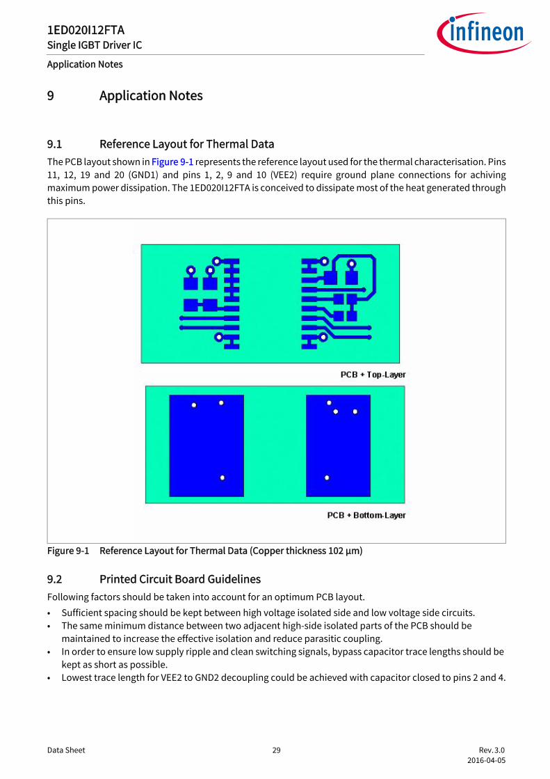
Package Outlines
Data Sheet 28 Rev. 3.0 2016-04-05
8 Package Outlines
Figure 8-1 PG-DSO-20 (Plastic (Green) Dual Small Outline Package)
1ED020I12FTASingle IGBT Driver IC
Application Notes
Data Sheet 29 Rev. 3.0 2016-04-05
9 Application Notes
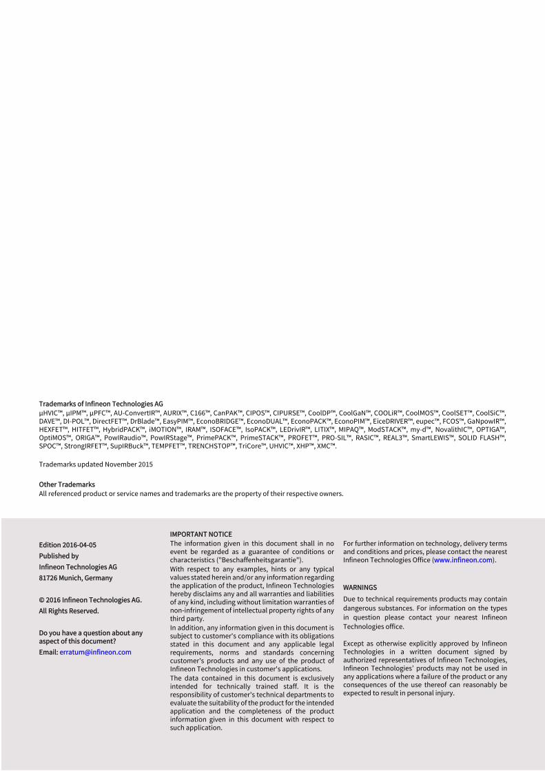
9.1 Reference Layout for Thermal DataThe PCB layout shown in Figure 9-1 represents the reference layout used for the thermal characterisation. Pins11, 12, 19 and 20 (GND1) and pins 1, 2, 9 and 10 (VEE2) require ground plane connections for achivingmaximum power dissipation. The 1ED020I12FTA is conceived to dissipate most of the heat generated throughthis pins.
Figure 9-1 Reference Layout for Thermal Data (Copper thickness 102 μm)
9.2 Printed Circuit Board GuidelinesFollowing factors should be taken into account for an optimum PCB layout.• Sufficient spacing should be kept between high voltage isolated side and low voltage side circuits.• The same minimum distance between two adjacent high-side isolated parts of the PCB should be
maintained to increase the effective isolation and reduce parasitic coupling.• In order to ensure low supply ripple and clean switching signals, bypass capacitor trace lengths should be
kept as short as possible.• Lowest trace length for VEE2 to GND2 decoupling could be achieved with capacitor closed to pins 2 and 4.
Do you have a question about any aspect of this document?Email: [email protected]
IMPORTANT NOTICEThe information given in this document shall in noevent be regarded as a guarantee of conditions orcharacteristics ("Beschaffenheitsgarantie"). With respect to any examples, hints or any typicalvalues stated herein and/or any information regardingthe application of the product, Infineon Technologieshereby disclaims any and all warranties and liabilitiesof any kind, including without limitation warranties ofnon-infringement of intellectual property rights of anythird party. In addition, any information given in this document issubject to customer's compliance with its obligationsstated in this document and any applicable legalrequirements, norms and standards concerningcustomer's products and any use of the product ofInfineon Technologies in customer's applications. The data contained in this document is exclusivelyintended for technically trained staff. It is theresponsibility of customer's technical departments toevaluate the suitability of the product for the intendedapplication and the completeness of the productinformation given in this document with respect tosuch application.
For further information on technology, delivery termsand conditions and prices, please contact the nearestInfineon Technologies Office (www.infineon.com).
WARNINGSDue to technical requirements products may containdangerous substances. For information on the typesin question please contact your nearest InfineonTechnologies office.
Except as otherwise explicitly approved by InfineonTechnologies in a written document signed byauthorized representatives of Infineon Technologies,Infineon Technologies’ products may not be used inany applications where a failure of the product or anyconsequences of the use thereof can reasonably beexpected to result in personal injury.
Please read the Important Notice and Warnings at the end of this document