www.ti.com SLOS242F –SEPTEMBER 2002–REVISED JANUARY 2010
2-GHz, LOW DISTORTION, DUAL CURRENT-FEEDBACK AMPLIFIERSCheck for Samples: THS3202
1FEATURES DESCRIPTION23• Unity-Gain Bandwidth: 2 GHz The THS3202 is a dual current-feedback amplifier
developed with BiCOM-II technology. Designed for• High Slew Rate: 9000 V/µslow distortion with a high slew rate of 9000 V/µs, the• High Output Current: ±115 mA into 20 Ω RL THS320x family is ideally suited for applications
• Power-Supply Voltage Range: 6.6 V to 15 V driving loads sensitive to distortion at highfrequencies.
APPLICATIONSThe THS3202 provides well-regulated ac
• High-Speed Signal Processing performance characteristics with power supplies• Test and Measurement Systems ranging from single-supply 6.6-V operation up to a• High-Voltage ADC Preamplifier 15-V supply. The high unity-gain bandwidth of up to
2 GHz is a major contributor to the excellent distortion• RF and IF Amplifier Stagesperformance. The THS3202 offers an output current• Professional Videodrive of ±115 mA and a low differential gain andphase error that make it suitable for applications suchas video line drivers.
The THS3202 is available in an SOIC-8, an MSOP-8,and an MSOP-8 with PowerPAD™ packages.
RELATED DEVICES AND DESCRIPTIONSTHS3001 ±15-V 420-MHz Low Distortion CFB Amplifier
Please be aware that an important notice concerning availability, standard warranty, and use in critical applications of TexasInstruments semiconductor products and disclaimers thereto appears at the end of this data sheet.
2PowerPAD is a trademark of Texas Instruments.3All other trademarks are the property of their respective owners.
SLOS242F –SEPTEMBER 2002–REVISED JANUARY 2010 www.ti.com
This integrated circuit can be damaged by ESD. Texas Instruments recommends that all integrated circuits be handled withappropriate precautions. Failure to observe proper handling and installation procedures can cause damage.
ESD damage can range from subtle performance degradation to complete device failure. Precision integrated circuits may be moresusceptible to damage because very small parametric changes could cause the device not to meet its published specifications.
(1) For the most current package and ordering information, see the Package Option Addendum at the end of this document, or see the TIweb site at www.ti.com.
(2) This package is available taped and reeled. To order this packaging option, add an R suffix to the part number (that is, THS3202DR).
ABSOLUTE MAXIMUM RATINGS (1)
Over operating free-air temperature range, unless otherwise noted.
UNIT
Supply voltage, VS 16.5 V
Input voltage, VI ±VS
Differential input voltage, VID ±3 V
Output current, IO(2) 175 mA
Continuous power dissipation See Package Dissipation Ratings Table
Maximum junction temperature, TJ(3) +150°C
Maximum junction temperature, continuous operation, long-term reliability, TJ(4) +125°C
Operating free-air temperature range, TA –40°C to +85°C
Storage temperature range, TSTG –65°C to +150°C
HBM 3000 V
ESD ratings: CDM 1500 V
MM 200 V
(1) The absolute maximum ratings under any condition is limited by the constraints of the silicon process. Stresses above these ratings maycause permanent damage. Exposure to absolute maximum conditions for extended periods may degrade device reliability. These arestress ratings only, and functional operation of the device at these or any other conditions beyond those specified is not implied.
(2) The THS3202 may incorporate a PowerPAD on the underside of the chip. This acts as a heat sink and must be connected to athermally dissipative plane for proper power dissipation. Failure to do so may result in exceeding the maximum junction temperaturewhich could permanently damage the device. See TI technical briefs SLMA002 and SLMA004 for more information about using thePowerPAD thermally-enhanced package.
(3) The absolute maximum temperature under any condition is limited by the constraints of the silicon process.(4) The maximum junction temperature for continuous operation is limited by package constraints. Operation above this temperature may
result in reduced reliability and/or lifetime of the device.
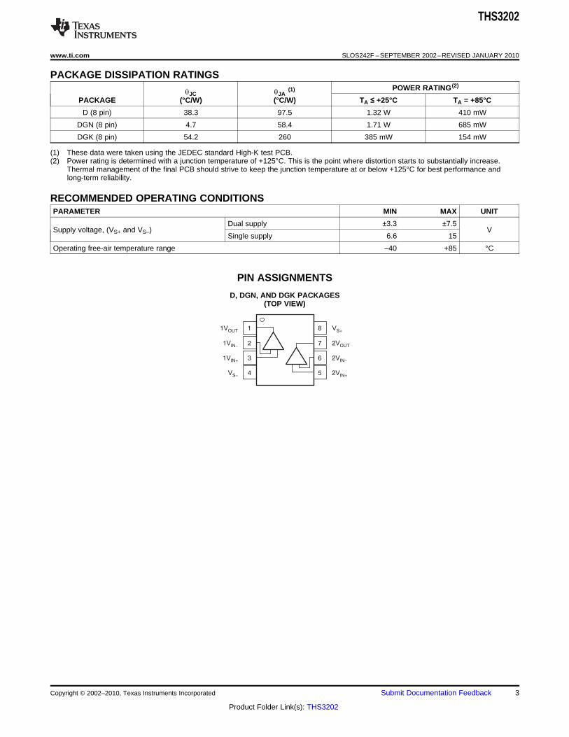
www.ti.com SLOS242F –SEPTEMBER 2002–REVISED JANUARY 2010
PACKAGE DISSIPATION RATINGSPOWER RATING (2)
qJC qJA(1)
PACKAGE (°C/W) (°C/W) TA ≤ +25°C TA = +85°C
D (8 pin) 38.3 97.5 1.32 W 410 mW
DGN (8 pin) 4.7 58.4 1.71 W 685 mW
DGK (8 pin) 54.2 260 385 mW 154 mW
(1) These data were taken using the JEDEC standard High-K test PCB.(2) Power rating is determined with a junction temperature of +125°C. This is the point where distortion starts to substantially increase.
Thermal management of the final PCB should strive to keep the junction temperature at or below +125°C for best performance andlong-term reliability.
RECOMMENDED OPERATING CONDITIONSPARAMETER MIN MAX UNIT
Dual supply ±3.3 ±7.5Supply voltage, (VS+ and VS–) V
www.ti.com SLOS242F –SEPTEMBER 2002–REVISED JANUARY 2010
APPLICATION INFORMATION
INTRODUCTION
The THS3202 is a high-speed, operational amplifier configured in a current-feedback architecture. The device isbuilt using Texas Instruments BiCOM-II process, a 15-V, dielectrically isolated, complementary bipolar processwith NPN and PNP transistors possessing fTs of several GHz. This configuration implements an exceptionallyhigh-performance amplifier that has a wide bandwidth, high slew rate, fast settling time, and low distortion.
RECOMMENDED FEEDBACK AND GAIN RESISTOR VALUES
As with all current-feedback amplifiers, the bandwidth of the THS3202 is an inversely proportional function of thevalue of the feedback resistor. The recommended resistors for the optimum frequency response are shown inTable 1. These should be used as a starting point and once optimum values are found, 1% tolerance resistorsshould be used to maintain frequency response characteristics. For most applications, a feedback resistor valueof 750 Ω is recommended—a good compromise between bandwidth and phase margin that yields a very stableamplifier.
Table 1. Recommended Resistor Values for Optimum Frequency Response
THS3202 RF FOR AC WHEN RLOAD = 100 ΩGAIN VSUP PEAKING RF VALUE
15 Optimum 6191
±5 Optimum 619
15 Optimum 5362
±5 Optimum 536
15 Optimum 4025
±5 Optimum 402
15 Optimum 20010
±5 Optimum 200
15 Optimum 450–1
±5 Optimum 450
As shown in Table 1, to maintain the highest bandwidth with an increasing gain, the feedback resistor is reduced.The advantage of dropping the feedback resistor (and the gain resistor) is that the noise of the system is alsoreduced compared to no reduction of these resistor values (see the Noise Calculations section). Thus, keepingthe bandwidth as high as possible maintains very good distortion performance of the amplifier by keeping theexcess loop gain as high as possible.
Care must be taken to not drop these values too low. The amplifier output must drive the feedback resistance(and gain resistance) and may place a burden on the amplifier. The end result is that distortion may actuallyincrease due to the low impedance load presented to the amplifier. Careful management of the amplifierbandwidth and the associated loading effects must be examined by the designer for optimum performance.
SLOS242F –SEPTEMBER 2002–REVISED JANUARY 2010 www.ti.com
The THS3202 amplifier exhibits very good distortion performance and bandwidth with the capability of utilizing upto 15-V supplies. Their excellent current drive capability of up to 115 mA driving into a 20-Ω load allows for manyversatile applications. One application is driving a twisted pair line (for example, a telephone line). Figure 77shows a simple circuit for driving a twisted pair differentially.
Figure 77. Simple Line Driver With THS3202
Due to the large power-supply voltages and the large current drive capability, power dissipation of the amplifiermust not be neglected. To have as much power dissipation as possible in a small package, the THS3202 isavailable in an MSOP-8 package (DGK), an MSOP-8 PowerPAD package (DGN), and an SOIC-8 package (D).Again, power dissipation of the amplifier must be carefully examined or else the amplifiers could become too hotand performance can be severely degraded. See the Power Dissipation and Thermal Considerations section formore information on thermal management.
T = Temperature in degrees Kelvin (273 +°C)Rf || Rg = Parallel resistance of Rf and Rg
eni en
2 IN RS
2 IN Rf Rg2 4 kTRs 4 kTRf Rg
eno eni AV eni1 RfRg (Noninverting Case)
THS3202
www.ti.com SLOS242F –SEPTEMBER 2002–REVISED JANUARY 2010
NOISE CALCULATIONS
Noise can cause errors on very small signals. This is especially true for amplifying small signals coming over atransmission line or an antenna. The noise model for current-feedback amplifiers (CFB) is the same as forvoltage feedback amplifiers (VFB). The only difference between the two is that CFB amplifiers generally specifydifferent current-noise parameters for each input, while VFB amplifiers usually only specify one noise-currentparameter. The noise model is shown in Figure 78. This model includes all of the noise sources as follows:• en = Amplifier internal voltage noise (nV/√Hz)• IN+ = Noninverting current noise (pA/√Hz)• IN− = Inverting current noise (pA/√Hz)• eRx = Thermal voltage noise associated with each resistor (eRx = 4 kTRx )
Figure 78. Noise Model
The total equivalent input noise density (eni) is calculated by using the following equation:
To get the equivalent output noise of the amplifier, multiply the equivalent input noise density (eni) by the overallamplifier gain (AV).
As the previous equations show, to keep noise at a minimum, small value resistors should be used. As theclosed-loop gain is increased (by reducing RF and RG), the input noise is reduced considerably because of theparallel resistance term. This leads to the general conclusion that the most dominant noise sources are thesource resistor (RS) and the internal amplifier noise voltage (en). Because noise is summed in aroot-mean-squares method, noise sources smaller than 25% of the largest noise source can be effectivelyignored. This can greatly simplify the formula and make noise calculations much easier.
SLOS242F –SEPTEMBER 2002–REVISED JANUARY 2010 www.ti.com
This brings up another noise measurement usually preferred in RF applications, the noise figure (NF). Noisefigure is a measure of noise degradation caused by the amplifier. The value of the source resistance must bedefined and is typically 50 Ω in RF applications.
Because the dominant noise components are generally the source resistance and the internal amplifier noisevoltage, we can approximate the noise figure as:
PRINTED-CIRCUIT BOARD LAYOUT TECHNIQUES FOR OPTIMAL PERFORMANCE
Achieving optimum performance with high-frequency amplifier-like devices in the THS320x family requires carefulattention to board layout parasitic and external component types.
Recommendations that optimize performance include:• Minimize parasitic capacitance to any ac ground for all of the signal I/O pins. Parasitic capacitance on the
output and input pins can cause instability. To reduce unwanted capacitance, a window around the signal I/Opins should be opened in all of the ground and power planes around those pins. Otherwise, ground andpower planes should be unbroken elsewhere on the board.
• Minimize the distance (< 0.25” or < 6,35 mm) from the power-supply pins to high-frequency 0.1-µF and 100pF decoupling capacitors. At the device pins, the ground and power-plane layout should not be in closeproximity to the signal I/O pins. Avoid narrow power and ground traces to minimize inductance between thepins and the decoupling capacitors. The power-supply connections should always be decoupled with thesecapacitors. Larger (6.8 µF or more) tantalum decoupling capacitors, effective at lower frequency, should alsobe used on the main supply pins. These may be placed somewhat farther from the device and may be sharedamong several devices in the same area of the printed circuit board (PCB). The primary goal is to minimizethe impedance seen in the differential-current return paths. For driving differential loads with the THS3202,adding a capacitor between the power-supply pins improves 2nd order harmonic distortion performance. Thisalso minimizes the current loop formed by the differential drive.
• Careful selection and placement of external components preserve the high-frequency performance of theTHS320x family. Resistors should be a very low reactance type. Surface-mount resistors work best and allowa tighter overall layout. Again, keep their leads and PCB trace length as short as possible. Never usewirewound type resistors in a high-frequency application. Because the output pin and inverting input pins arethe most sensitive to parasitic capacitance, always position the feedback and series output resistors, if any,as close as possible to the inverting input pins and output pins. Other network components, such as inputtermination resistors, should be placed close to the gain-setting resistors. Even with a low parasiticcapacitance shunting the external resistors, excessively high resistor values can create significant timeconstants that can degrade performance. Good axial metal-film or surface-mount resistors haveapproximately 0.2 pF in shunt with the resistor. For resistor values greater than 2.0 kΩ, this parasiticcapacitance can add a pole and/or a zero that can affect circuit operation. Keep resistor values as low aspossible, consistent with load driving considerations.
• Connections to other wideband devices on the board may be made with short direct traces or throughonboard transmission lines. For short connections, consider the trace and the input to the next device as alumped capacitive load. Relatively wide traces (50 mils to 100 mils or 1,27 mm to 2,54 mm) should be used,preferably with ground and power planes opened up around them. Estimate the total capacitive load anddetermine if isolation resistors on the outputs are necessary. Low parasitic capacitive loads (less than 4 pF)may not need an RS because the THS320x family is nominally compensated to operate with a 2-pF parasiticload. Higher parasitic capacitive loads without an RS are allowed as the signal gain increases (increasing theunloaded phase margin). If a long trace is required, and the 6-dB signal loss intrinsic to a doubly-terminated
www.ti.com SLOS242F –SEPTEMBER 2002–REVISED JANUARY 2010
transmission line is acceptable, implement a matched impedance transmission line using microstrip orstripline techniques (consult an ECL design handbook for microstrip and stripline layout techniques).A 50-Ω environment is not necessary onboard, and in fact, a higher impedance environment improvesdistortion as shown in the distortion versus load plots. With a characteristic board trace impedance based onboard material and trace dimensions, a matching series resistor into the trace from the output of the THS320xis used as well as a terminating shunt resistor at the input of the destination device.Remember also that the terminating impedance is the parallel combination of the shunt resistor and the inputimpedance of the destination device: this total effective impedance should be set to match the traceimpedance. If the 6-dB attenuation of a doubly-terminated transmission line is unacceptable, a long trace canbe series-terminated at the source end only. Treat the trace as a capacitive load in this case. This does notpreserve signal integrity as well as a doubly-terminated line. If the input impedance of the destination deviceis low, there is some signal attenuation due to the voltage divider formed by the series output into theterminating impedance.
• Socketing a high-speed part like the THS320x family is not recommended. The additional lead length andpin-to-pin capacitance introduced by the socket can create an extremely troublesome parasitic network whichcan make it almost impossible to achieve a smooth, stable frequency response. Best results are obtained bysoldering the THS320x family devices directly onto the board.
PowerPAD DESIGN CONSIDERATIONS
The THS320x family is available in a thermally-enhanced PowerPAD family of packages. These packages areconstructed using a downset leadframe upon which the die is mounted [see Figure 79(a) and Figure 79(b)]. Thisarrangement results in the lead frame being exposed as a thermal pad on the underside of the package [seeFigure 79(c)]. Because this thermal pad has direct thermal contact with the die, excellent thermal performancecan be achieved by providing a good thermal path away from the thermal pad.
The PowerPAD package allows for both assembly and thermal management in one manufacturing operation.During the surface-mount solder operation (when the leads are being soldered), the thermal pad can also besoldered to a copper area underneath the package. Through the use of thermal paths within this copper area,heat can be conducted away from the package into either a ground plane or other heat dissipating device.
The PowerPAD package represents a breakthrough in combining the small area and ease of assembly ofsurface mount with the, heretofore, awkward mechanical methods of heatsinking.
Figure 79. Views of Thermally-Enhanced Package
Although there are many ways to properly heatsink the PowerPAD package, the following steps illustrate therecommended approach.
where:PDmax is the maximum power dissipation in the amplifier (W).Tmax is the absolute maximum junction temperature (°C).TA is the ambient temperature (°C).θJA = θJC + θCAθJC is the thermal coefficient from the silicon junctions to the case (°C/W).θCA is the thermal coefficient from the case to ambient air (°C/W).
THS3202
SLOS242F –SEPTEMBER 2002–REVISED JANUARY 2010 www.ti.com
PowerPAD PCB LAYOUT CONSIDERATIONS1. Prepare the PCB with a top side etch pattern as shown in Figure 80. There should be etch for the leads as
well as etch for the thermal pad.
Figure 80. DGN PowerPAD PCB Etch and Via Pattern
2. Place five holes in the area of the thermal pad. These holes should be 10 mils (0,254 mm) in diameter. Keepthem small so that solder wicking through the holes is not a problem during reflow.
3. Additional vias may be placed anywhere along the thermal plane outside of the thermal pad area. This helpsdissipate the heat generated by the THS320x family IC. These additional vias may be larger than the 10-mildiameter vias directly under the thermal pad. They can be larger because they are not in the thermal padarea to be soldered so that wicking is not a problem.
4. Connect all holes to the internal ground plane.5. When connecting these holes to the ground plane, do not use the typical web or spoke via connection
methodology. Web connections have a high thermal resistance connection that is useful for slowing the heattransfer during soldering operations. This makes the soldering of vias that have plane connections easier. Inthis application, however, low thermal resistance is desired for the most efficient heat transfer. Therefore, theholes under the THS320x family PowerPAD package should make their connection to the internal groundplane with a complete connection around the entire circumference of the plated-through hole.
6. The top-side solder mask should leave the terminals of the package and the thermal pad area with its fiveholes exposed. The bottom-side solder mask should cover the five holes of the thermal pad area. Thisprevents solder from being pulled away from the thermal pad area during the reflow process.
7. Apply solder paste to the exposed thermal pad area and all of the IC terminals.8. With these preparatory steps in place, the IC is simply placed in position and run through the solder reflow
operation as any standard surface-mount component. This results in a part that is properly installed.
POWER DISSIPATION AND THERMAL CONSIDERATIONS
To maintain maximum output capabilities, the THS3202 does not incorporate automatic thermal shutoffprotection. The designer must take care to ensure that the design does not violate the absolute maximumjunction temperature of the device. Failure may result if the absolute maximum junction temperature of +150°C isexceeded. For best performance, design for a maximum junction temperature of +125°C. Between +125°C and+150°C, damage does not occur, but the performance of the amplifier begins to degrade.
The thermal characteristics of the device are dictated by the package and the PCB. Maximum power dissipationfor a given package can be calculated using the following formula.
θJA = 58.4°C/W for 8-Pin MSOP w/PowerPad (DGN)θJA = 98°C/W for 8-Pin SOIC High T est PCB (D)θJA = 158°C/W for 8-Pin MSOP w/PowerPad w/o Solder
Results are With No Air Flow and PCB Size = 3”x3”
0.0
0.5
1.0
1.5
2.0
2.5
3.0
3.5
4.0
−40 −20 0 20 40 60 80 100
PD
− M
axim
um P
ower
Dis
sipa
tion
− W
TA − Free-Air T emperature − °C
θJA = 98°C/W
θJA = 158°C/W
TJ = 125°C
θJA = 58.4°C/W
+
_
THS3202
CLOAD
Rg
Input
Output
Rf
10 Ω
THS3202
www.ti.com SLOS242F –SEPTEMBER 2002–REVISED JANUARY 2010
For systems where heat dissipation is more critical, the THS320x family of devices is offered in an MSOP-8 withPowerPAD. The thermal coefficient for the PowerPAD packages are substantially improved over the traditionalSOIC. Maximum power dissipation levels are depicted in the graph for the available packages. The data for thePowerPAD packages assume a board layout that follows the PowerPAD layout guidelines referenced above anddetailed in the PowerPAD application note number SLMA002. The following graph also illustrates the effect ofnot soldering the PowerPAD to a PCB. The thermal impedance increases substantially which may cause seriousheat and performance issues. Be sure to always solder the PowerPAD to the PCB for optimum performance.
Figure 81. Maximum Power Dissipation vs Ambient Temperature
When determining whether or not the device satisfies the maximum power dissipation requirement, it is importantto not only consider quiescent power dissipation, but also dynamic power dissipation. Often times, this is difficultto quantify because the signal pattern is inconsistent, but an estimate of the RMS power dissipation can providevisibility into a possible problem.
DRIVING A CAPACITIVE LOAD
Driving capacitive loads with high-performance amplifiers is not a problem as long as certain precautions aretaken. The first is to realize that the THS3202 has been internally compensated to maximize its bandwidth andslew-rate performance. When the amplifier is compensated in this manner, capacitive loading directly on theoutput decreases the device's phase margin leading to high-frequency ringing or oscillations. Therefore, forcapacitive loads of greater than 10 pF, it is recommended that a resistor be placed in series with the output ofthe amplifier, as shown in Figure 82. A minimum value of 10 Ω should work well for most applications. Forexample, in 75-Ω transmission systems, setting the series resistor value to 75 Ω both isolates any capacitanceloading and provides the proper line impedance matching at the source end.
SLOS242F –SEPTEMBER 2002–REVISED JANUARY 2010 www.ti.com
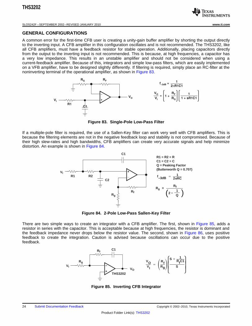
GENERAL CONFIGURATIONS
A common error for the first-time CFB user is creating a unity-gain buffer amplifier by shorting the output directlyto the inverting input. A CFB amplifier in this configuration oscillates and is not recommended. The THS3202, likeall CFB amplifiers, must have a feedback resistor for stable operation. Additionally, placing capacitors directlyfrom the output to the inverting input is not recommended. This is because, at high frequencies, a capacitor hasa very low impedance. This results in an unstable amplifier and should not be considered when using acurrent-feedback amplifier. Because of this, integrators and simple low-pass filters, which are easily implementedon a VFB amplifier, have to be designed slightly differently. If filtering is required, simply place an RC-filter at thenoninverting terminal of the operational amplifier, as shown in Figure 83.
Figure 83. Single-Pole Low-Pass Filter
If a multiple-pole filter is required, the use of a Sallen-Key filter can work very well with CFB amplifiers. This isbecause the filtering elements are not in the negative feedback loop and stability is not compromised. Because oftheir high slew-rates and high bandwidths, CFB amplifiers can create very accurate signals and help minimizedistortion. An example is shown in Figure 84.
Figure 84. 2-Pole Low-Pass Sallen-Key Filter
There are two simple ways to create an integrator with a CFB amplifier. The first, shown in Figure 85, adds aresistor in series with the capacitor. This is acceptable because at high frequencies, the resistor is dominant andthe feedback impedance never drops below the resistor value. The second, shown in Figure 86, uses positivefeedback to create the integration. Caution is advised because oscillations can occur due to the positivefeedback.
www.ti.com SLOS242F –SEPTEMBER 2002–REVISED JANUARY 2010
Figure 86. Noninverting CFB Integrator
The THS3202 may also be employed as a very good video distribution amplifier. One characteristic of distributionamplifiers is the fact that the differential phase (DP) and the differential gain (DG) are compromised as thenumber of lines increase and the closed-loop gain increases. Be sure to use termination resistors throughout thedistribution system to minimize reflections and capacitive loading.
Figure 87. Video Distribution Amplifier Application
SLOS242F –SEPTEMBER 2002–REVISED JANUARY 2010 www.ti.com
REVISION HISTORY
NOTE: Page numbers for previous revisions may differ from page numbers in the current version.
Changes from Revision E (April 2009) to Revision F Page
• Updated document format to current standards ................................................................................................................... 1
• Deleted lead temperature specification from Absolute Maximum Ratings table .................................................................. 2
• Changed first sentence of third paragraph of Power Dissipation and Thermal Considerations section ............................ 23
Changes from Revision D (January 2009) to Revision E Page
• Deleted feature bullets relating to IMD3 and OIP3 at VCC = 15 V ........................................................................................ 1
• Changed text in first sentence of Description section ........................................................................................................... 1
• Deleted harmonic distortion specifications in AC Performance subsection for VCC = 15 V .................................................. 6
• Deleted harmonic distortion graphs for VCC = 15 V ............................................................................................................ 10
THS3202DGK NRND VSSOP DGK 8 80 Green (RoHS& no Sb/Br)
CU NIPDAU Level-1-260C-UNLIM -40 to 85 BEV
THS3202DGKG4 NRND VSSOP DGK 8 80 Green (RoHS& no Sb/Br)
CU NIPDAU Level-1-260C-UNLIM -40 to 85 BEV
THS3202DGN NRND MSOP-PowerPAD
DGN 8 80 Green (RoHS& no Sb/Br)
CU NIPDAU |CU NIPDAUAG
Level-1-260C-UNLIM -40 to 85 BEP
THS3202DGNG4 NRND MSOP-PowerPAD
DGN 8 80 Green (RoHS& no Sb/Br)
CU NIPDAUAG Level-1-260C-UNLIM -40 to 85 BEP
THS3202DGNR NRND MSOP-PowerPAD
DGN 8 2500 Green (RoHS& no Sb/Br)
CU NIPDAU |CU NIPDAUAG
Level-1-260C-UNLIM -40 to 85 BEP
THS3202DGNRG4 NRND MSOP-PowerPAD
DGN 8 2500 Green (RoHS& no Sb/Br)
CU NIPDAUAG Level-1-260C-UNLIM -40 to 85 BEP
(1) The marketing status values are defined as follows:ACTIVE: Product device recommended for new designs.LIFEBUY: TI has announced that the device will be discontinued, and a lifetime-buy period is in effect.NRND: Not recommended for new designs. Device is in production to support existing customers, but TI does not recommend using this part in a new design.PREVIEW: Device has been announced but is not in production. Samples may or may not be available.OBSOLETE: TI has discontinued the production of the device.
(2) RoHS: TI defines "RoHS" to mean semiconductor products that are compliant with the current EU RoHS requirements for all 10 RoHS substances, including the requirement that RoHS substancedo not exceed 0.1% by weight in homogeneous materials. Where designed to be soldered at high temperatures, "RoHS" products are suitable for use in specified lead-free processes. TI mayreference these types of products as "Pb-Free".RoHS Exempt: TI defines "RoHS Exempt" to mean products that contain lead but are compliant with EU RoHS pursuant to a specific EU RoHS exemption.Green: TI defines "Green" to mean the content of Chlorine (Cl) and Bromine (Br) based flame retardants meet JS709B low halogen requirements of <=1000ppm threshold. Antimony trioxide basedflame retardants must also meet the <=1000ppm threshold requirement.
(3) MSL, Peak Temp. - The Moisture Sensitivity Level rating according to the JEDEC industry standard classifications, and peak solder temperature.
(4) There may be additional marking, which relates to the logo, the lot trace code information, or the environmental category on the device.
(5) Multiple Device Markings will be inside parentheses. Only one Device Marking contained in parentheses and separated by a "~" will appear on a device. If a line is indented then it is a continuationof the previous line and the two combined represent the entire Device Marking for that device.
PACKAGE OPTION ADDENDUM
www.ti.com 24-Aug-2018
Addendum-Page 2
(6) Lead/Ball Finish - Orderable Devices may have multiple material finish options. Finish options are separated by a vertical ruled line. Lead/Ball Finish values may wrap to two lines if the finishvalue exceeds the maximum column width.
Important Information and Disclaimer:The information provided on this page represents TI's knowledge and belief as of the date that it is provided. TI bases its knowledge and belief on informationprovided by third parties, and makes no representation or warranty as to the accuracy of such information. Efforts are underway to better integrate information from third parties. TI has taken andcontinues to take reasonable steps to provide representative and accurate information but may not have conducted destructive testing or chemical analysis on incoming materials and chemicals.TI and TI suppliers consider certain information to be proprietary, and thus CAS numbers and other limited information may not be available for release.
In no event shall TI's liability arising out of such information exceed the total purchase price of the TI part(s) at issue in this document sold by TI to Customer on an annual basis.
Texas Instruments Incorporated (TI) reserves the right to make corrections, enhancements, improvements and other changes to itssemiconductor products and services per JESD46, latest issue, and to discontinue any product or service per JESD48, latest issue. Buyersshould obtain the latest relevant information before placing orders and should verify that such information is current and complete.TI’s published terms of sale for semiconductor products (http://www.ti.com/sc/docs/stdterms.htm) apply to the sale of packaged integratedcircuit products that TI has qualified and released to market. Additional terms may apply to the use or sale of other types of TI products andservices.Reproduction of significant portions of TI information in TI data sheets is permissible only if reproduction is without alteration and isaccompanied by all associated warranties, conditions, limitations, and notices. TI is not responsible or liable for such reproduceddocumentation. Information of third parties may be subject to additional restrictions. Resale of TI products or services with statementsdifferent from or beyond the parameters stated by TI for that product or service voids all express and any implied warranties for theassociated TI product or service and is an unfair and deceptive business practice. TI is not responsible or liable for any such statements.Buyers and others who are developing systems that incorporate TI products (collectively, “Designers”) understand and agree that Designersremain responsible for using their independent analysis, evaluation and judgment in designing their applications and that Designers havefull and exclusive responsibility to assure the safety of Designers' applications and compliance of their applications (and of all TI productsused in or for Designers’ applications) with all applicable regulations, laws and other applicable requirements. Designer represents that, withrespect to their applications, Designer has all the necessary expertise to create and implement safeguards that (1) anticipate dangerousconsequences of failures, (2) monitor failures and their consequences, and (3) lessen the likelihood of failures that might cause harm andtake appropriate actions. Designer agrees that prior to using or distributing any applications that include TI products, Designer willthoroughly test such applications and the functionality of such TI products as used in such applications.TI’s provision of technical, application or other design advice, quality characterization, reliability data or other services or information,including, but not limited to, reference designs and materials relating to evaluation modules, (collectively, “TI Resources”) are intended toassist designers who are developing applications that incorporate TI products; by downloading, accessing or using TI Resources in anyway, Designer (individually or, if Designer is acting on behalf of a company, Designer’s company) agrees to use any particular TI Resourcesolely for this purpose and subject to the terms of this Notice.TI’s provision of TI Resources does not expand or otherwise alter TI’s applicable published warranties or warranty disclaimers for TIproducts, and no additional obligations or liabilities arise from TI providing such TI Resources. TI reserves the right to make corrections,enhancements, improvements and other changes to its TI Resources. TI has not conducted any testing other than that specificallydescribed in the published documentation for a particular TI Resource.Designer is authorized to use, copy and modify any individual TI Resource only in connection with the development of applications thatinclude the TI product(s) identified in such TI Resource. NO OTHER LICENSE, EXPRESS OR IMPLIED, BY ESTOPPEL OR OTHERWISETO ANY OTHER TI INTELLECTUAL PROPERTY RIGHT, AND NO LICENSE TO ANY TECHNOLOGY OR INTELLECTUAL PROPERTYRIGHT OF TI OR ANY THIRD PARTY IS GRANTED HEREIN, including but not limited to any patent right, copyright, mask work right, orother intellectual property right relating to any combination, machine, or process in which TI products or services are used. Informationregarding or referencing third-party products or services does not constitute a license to use such products or services, or a warranty orendorsement thereof. Use of TI Resources may require a license from a third party under the patents or other intellectual property of thethird party, or a license from TI under the patents or other intellectual property of TI.TI RESOURCES ARE PROVIDED “AS IS” AND WITH ALL FAULTS. TI DISCLAIMS ALL OTHER WARRANTIES ORREPRESENTATIONS, EXPRESS OR IMPLIED, REGARDING RESOURCES OR USE THEREOF, INCLUDING BUT NOT LIMITED TOACCURACY OR COMPLETENESS, TITLE, ANY EPIDEMIC FAILURE WARRANTY AND ANY IMPLIED WARRANTIES OFMERCHANTABILITY, FITNESS FOR A PARTICULAR PURPOSE, AND NON-INFRINGEMENT OF ANY THIRD PARTY INTELLECTUALPROPERTY RIGHTS. TI SHALL NOT BE LIABLE FOR AND SHALL NOT DEFEND OR INDEMNIFY DESIGNER AGAINST ANY CLAIM,INCLUDING BUT NOT LIMITED TO ANY INFRINGEMENT CLAIM THAT RELATES TO OR IS BASED ON ANY COMBINATION OFPRODUCTS EVEN IF DESCRIBED IN TI RESOURCES OR OTHERWISE. IN NO EVENT SHALL TI BE LIABLE FOR ANY ACTUAL,DIRECT, SPECIAL, COLLATERAL, INDIRECT, PUNITIVE, INCIDENTAL, CONSEQUENTIAL OR EXEMPLARY DAMAGES INCONNECTION WITH OR ARISING OUT OF TI RESOURCES OR USE THEREOF, AND REGARDLESS OF WHETHER TI HAS BEENADVISED OF THE POSSIBILITY OF SUCH DAMAGES.Unless TI has explicitly designated an individual product as meeting the requirements of a particular industry standard (e.g., ISO/TS 16949and ISO 26262), TI is not responsible for any failure to meet such industry standard requirements.Where TI specifically promotes products as facilitating functional safety or as compliant with industry functional safety standards, suchproducts are intended to help enable customers to design and create their own applications that meet applicable functional safety standardsand requirements. Using products in an application does not by itself establish any safety features in the application. Designers mustensure compliance with safety-related requirements and standards applicable to their applications. Designer may not use any TI products inlife-critical medical equipment unless authorized officers of the parties have executed a special contract specifically governing such use.Life-critical medical equipment is medical equipment where failure of such equipment would cause serious bodily injury or death (e.g., lifesupport, pacemakers, defibrillators, heart pumps, neurostimulators, and implantables). Such equipment includes, without limitation, allmedical devices identified by the U.S. Food and Drug Administration as Class III devices and equivalent classifications outside the U.S.TI may expressly designate certain products as completing a particular qualification (e.g., Q100, Military Grade, or Enhanced Product).Designers agree that it has the necessary expertise to select the product with the appropriate qualification designation for their applicationsand that proper product selection is at Designers’ own risk. Designers are solely responsible for compliance with all legal and regulatoryrequirements in connection with such selection.Designer will fully indemnify TI and its representatives against any damages, costs, losses, and/or liabilities arising out of Designer’s non-compliance with the terms and provisions of this Notice.


![INDUSTRIAL PNEUMATICS - fittings€¦ · MW-2007003 6 MW-2L07004 8 MW-2007005 10 MW-2007006 12 MW-2007007 14 Tee adapter, brass R 5 code hose O.D. [mm] MW-2005A02 3 MW-2005A01 3.17](https://static.documents.pub/doc/80x56/6020b0177745f5137a1d1da5/industrial-pneumatics-fittings-mw-2007003-6-mw-2l07004-8-mw-2007005-10-mw-2007006.jpg)


