Abstract— Monolithic 3-D (M3D) IC is one of the potentialtechnologies to break through the challenges of continued circuitpower and performance scaling. In this paper, for the first time,we demonstrate the power benefits of M3D and present designguideline in a 7-nm FinFET technology node. The predictive 7-nmprocess design kit (PDK) and the standard cell library using bothhigh-performance (HP) and low-standby-power (LSTP) devicetechnologies are developed based on NanGate 45-nm PDK usingaccurate dimensional, material, and electrical parameters frompublications and a commercial-grade tool flow. We implementfull-chip M3D designs utilizing industry-standard physical designtools, and gauge the impact of M3D technology on performance,power, and area metrics. We also provide the design guidelinesas well as a new partitioning methodology to improve M3Ddesign quality. This paper shows that M3D designs outperform2-D counterparts by 16% and 16.5% on average in terms ofisoperformance total power reduction with 7-nm HP and LSTPcell library, respectively. This demonstrates the power benefitsof M3D technology in both HP and low-power future generationdevices.
Index Terms— 7-nm technology, design quality, FinFET,monolithic 3-D (M3D) IC.
I. INTRODUCTION
AS TECHNOLOGY scaling faces its physical limits inchannel length scaling, degrading process variations,
lithography constraints, increased parasitics, and rising man-ufacturing costs, monolithic 3-D (M3D) takes center stage incontinuing Moore’s law. In the M3D technology, the devicesare fabricated onto multiple tiers sequentially with nanosizedmonolithic intertier vias (MIVs), which connect the top metallayer of the bottom tier and the bottom metal layer of the toptier. Because MIVs are extremely small, we can achieve muchhigher density and lower parasitics compared with through-silicon vias, which is another method of 3-D design. Thanksto the enhancement of fabrication technology such as higheralignment precision and thinner die, we can harness the truebenefit of M3D with fine-grained vertical integration [1].
Manuscript received October 11, 2016; revised January 18, 2017; acceptedFebruary 20, 2017. Date of publication April 5, 2017; date of current versionJune 23, 2017. This work was supported by ARM Inc.
K. Chang, K. Acharya, and S. K. Lim are with the School of Electricaland Computer Engineering, Georgia Institute of Technology, Atlanta,GA 30332 USA (e-mail: [email protected]; [email protected];[email protected]).
Color versions of one or more of the figures in this paper are availableonline at http://ieeexplore.ieee.org.
Digital Object Identifier 10.1109/TVLSI.2017.2686426
Fig. 1. Structure of M3D IC based on FinFET transistors.
This paper is to understand the benefit and tradeoffsinvolved in using gate-level M3D, which utilizes places stan-dard cells into multiple tiers and uses MIVs only for intercellconnections, at the end of silicon scaling, and hence, we havetargeted the 7-nm technology node. By 7 nm, devices will havetransitioned from planar to FinFET in order to counteract thelimits of degrading short-channel effects, process variations,and reliability degradation. Therefore, important tools, and,to the best of our knowledge, the only open-source 7-nm Fin-FET transistor models for this study are Predictive TechnologyModels for Multi-Gate (PTM-MG) [2].
While M3D technology based on planar MOSFETs hasbeen studied actively, FinFET implementations have not beenwidely explored. A study on the benefits of M3D on a 7-nmtechnology has been investigated in [3]. However, the authorsmanually derived intracell RC parasitics with a simple calcula-tion instead of utilizing commercial tools for extraction. Theirlibrary also contains only six cells and did not consider thestructure and effects of FinFET technology during cell design,which is prone to inaccuracies.
In this paper, we present the power benefit of gate-levelM3D technology at the advanced technology nodes (i.e.,7-nm FinFET technology node) (see Fig. 1). The majorcontributions of this paper are as follows: 1) we devel-oped a predictive 7-nm process design kit (PDK) basedon FinFET transistors and corresponding high perfor-mance (HP) and low-standby-power (LSTP) standard celllibraries with 122 cells using commercial-grade electronicdesign automation (EDA) tools; 2) we used the developed
CHANG et al.: IMPACT AND DESIGN GUIDELINE OF MONOLITHIC 3-D IC AT THE 7-nm TECHNOLOGY NODE 2119
TABLE I
KEY PARAMETERS IN NANGATE 45-nm AND OUR 7-nm PDK
7-nm libraries to implement full-chip gate-level M3D designsusing the state-of-art gate-level M3D design flow [4];3) we investigated the impact of gate-level M3D technology onpower consumption at the 7-nm FinFET technology node forboth HP and LSTP cells using the full-chip GDS layouts; and4) we presented guidelines and a new clock tree partitioningmethodology to maximize the benefit of M3D technology inthe advanced technology nodes. To the best of our knowledge,this is the first work that studies both full-chip 2-D andM3D designs at the 7-nm FinFET technology node.
II. 7-nm PDK GENERATION
In order to properly evaluate the benefits of M3D tech-nology on a 7-nm FinFET node, the corresponding PDK isneeded for standard cell design and M3D synthesis, place androute (P&R). Since an open-source 7-nm FinFET PDK is notreadily available to the research community, we created ourown and validated it. We started with NanGate 45-nm PDKand scaled all technology parameters to values correspondingto the 7-nm node. Fig. 2 presents the procedure used to developour predictive 7-nm PDK.
A. Technology Modeling and PDK Generation
The 7-nm PDK is defined based on the minimum dimen-sions of each layer in the process and accurate modeling ofthe transistor and interconnect behavior.
1) Dimensional Scaling: Table I shows the minimumdimensions and material properties assumed in the 7-nm PDK.Channel length scaling has been less aggressive insub-45-nm technology nodes and is no longer the primaryparameter defining the technology node. However, contactedpoly-pitch (CPP) and M1 pitch scale by about 0.7 times everynode and are better indicators of expected area scaling. Based
on industry trends and [5], we settled on the values of 35 nmfor M1 pitch and 48-nm CPP for 7 nm. To scale the 45-nmlayouts to 7-nm dimensions, we used the geometric mean ofthe M1 pitch and CPP to get our scaling factor of 0.25.1
For interconnect dimensions, all x − y dimensions of wiresare scaled from the 45-nm PDK by the same scaling factorof 0.25, but the aspect ratios (thickness/width) are set to2 based on ITRS projections. The dielectric thicknesses arescaled proportionately from the 45-nm PDK.
2) Interconnect Modeling: The 7-nm PDK requires accu-rate modeling of interconnect parameters, such as conductorsheet resistance, via, and contact resistance. We assumedcopper (Cu) is used for metal layers, and the resistivity ofthe M1–M6 layers is determined to be 6.35 and 1.9 μ�-cmfor M7–M10, based on ITRS projections. One of the mainreasons for the increased resistivity is the increased scatteringexperienced at grain boundaries within the Cu wires [6]. Dueto the increased resistivity and the diminished cross-sectionalarea, the sheet resistances of the 7-nm technology are largerthan that of NanGate 45-nm PDK, as shown in Table I.
For vias, Cu is assumed for via material with tantalumnitride (TaN) barrier. A barrier is necessary between a Cuvia and the corresponding dielectric layer in order to preventCu atoms from diffusing into and contaminating the dielectriclayer. The resistivity of Cu is based on ITRS projections, whilethe resistivity of TaN is determined to be 2000 μ�-cm [7].Table I presents the resulting via resistance for each layer.
Contacts from M1 to active and poly utilize tungsten (W)instead of Cu because of their excellent step coverage andgap fill abilities, especially for high-aspect ratio fills. Addi-tionally, tungsten silicide (WSi2) allows for low resistancecontacts to the transistors. The resistivity of W contacts isdetermined to be 30 μ�-cm as projected in [8], which yielded27.3 and 46.14 � for the resistance of Active-M1 contacts andPoly-M1 contacts, respectively.
3) Layout Scaling: Ever since the introduction of multiplepatterning for min-pitch metals in sub-20-nm nodes, tungstenlocal interconnects (also called middle of line, MOL layers)are used for cell level routing. Since standard cell layoutswith these features are not available publicly, we scaled45-nm layouts to 7-nm dimensions, but MOL layers are notmodeled in this paper. This will result in some optimism whenestimating cell level parasitics, but the larger scope of thispaper remains unaffected, because important parameters suchas transistor behavior and interconnect parasitics are accuratelymodeled. The goal of this paper is to understand importanttrends and tradeoffs when working with future technologies.
The cell widths and heights of the NanGate 45-nm librarywere shrunk along the x − y dimension with the scalingfactor derived in Section II-A1. For planar transistors, elec-tron mobility is higher compared with holes, and hence,pMOS transistors are sized wider. In sub-45-nm technologies,strain engineering improves carrier mobility and has beenan important knob to improve performance every technologynode. Additionally, pMOS transistors benefit more from strain
1Due to precision problems with the EDA tools, the scaling factor is roundedto two decimal places.
2120 IEEE TRANSACTIONS ON VERY LARGE SCALE INTEGRATION (VLSI) SYSTEMS, VOL. 25, NO. 7, JULY 2017
Fig. 3. Comparison of NAND2_X2 cell GDS layouts between (a) NanGate45-nm PDK and (b) our 7-nm PDK.
resulting in nearly equal current drive strengths as nMOS [9].Hence, after scaling the 45-nm planar layouts, the pMOS issized equal to nMOS in order to balance cell rise and fall time.
An example 7-nm cell GDS layout of NAND2_X2 iscompared with its NanGate 45-nm PDK layout in Fig. 3.As shown in the figure, though cell height and width are scaleddown according to the geometric scaling factor, pMOS widthis shrunk further to balance drive strength.
B. 7-nm Standard Cell Library
LEF views are created from 7-nm layout GDS files tobe used for full-chip implementation by Cadence abstractgenerator. Interconnect dimensions and material propertiesdiscussed in Section II-A are coded in an MIPT file and isused to generate lookup tables for intracell parasitic data usingMentor Graphics Calibre xRC. These lookup tables, along withthe scaled cell GDS layouts and LVS file, are used to extract7-nm SPICE netlists with parastics for every cell using MentorGraphics Calibre xRC.
1) Planar Width to Quantized Fins: Since our 7-nm layoutsare scaled from 45-nm layouts assuming planar transistors,the device widths have to be appropriately quantized to fins.The maximum number of fins in a standard cell is determinedby the standard cell height and the ratio between metal pitch
TABLE II
MAXIMUM NUMBER OF FINS AND THE FINGER COUNTIN VARIOUS DRIVE-STRENGTH INVERTERS
and fin pitch. We have the assumptions for dummy fins inour layouts, which are also required to make room for gatecontacts between the FETs and to allow isolation betweenFETs in adjacent cell rows. Therefore, the number of fins in apMOS and nMOS pair is limited by the number of M1 trackssubtracted by the number of dummy fins. As shown in Table I,our scaled design has 10 M1 tracks, and we assume a fin pitchof 25.5 nm to fit four fins per FET, which is in line withindustry trends [5]. With an assumption of two dummy finsper pMOS and nMOS pair, dividing the transistor width byfin pitch gives us the number of fins for that device.
Table II shows the maximum number of fins as well asthe number of fingers derived using our method for variousdrive-strength cells of inverter. The low drive-strength inverters(i.e., INV_X1 to INV_X4) gain strength by increasingtheir number of fins, while the high drive-strength inverters(i.e., INV_X8 to INV_X32) do so by increasing their numberof fingers.
Using the method, we generated the new SPICE netlistswith FinFETs. We, then, used the netlists and ASU PTM-MGFinFET transistor models for both HP and LSTP applica-tions [10] to extract timing and power metrics (LIB) usingSynopsys SiliconSmart.
C. 7-nm Library Characterization
We generated our 7-nm HP and LSTP libraries with total122 cells. Table III shows cell delay, internal power-delayproduct (PDP), and leakage power of ten selected cells com-paring NanGate 45 nm, 7-nm HP, and 7-nm LSTP libraries.2
Fig. 4 also shows the I–V characteristics of the transistormodels used in cell characterization.
Compared with NanGate 45 nm, 7-nm HP library has 84.7%lower cell delay on average. Due to the decrease in cell delay,voltage scaling, and smaller input capacitance, the internalPDP of our 7-nm HP cells is reduced significantly. A leakagepower consumption of 7-nm HP cells is also 69.5% smalleron average, mainly due to the reduced dimension and sup-ply voltage even though 7-nm HP transistor model showshigher IOFF. The 7-nm LSTP library has longer cell delaycompared with 7-nm HP library because of smaller ION oflower leakage transistors as shown in Fig. 4, but the internalPDP of LSTP cells is lower than HP cells. Since 7-nm LSTPtransistor model is designed to specifically reduce its leakagepower consumption, it exhibits much smaller IOFF than the
2In order to obtain a fair comparison between different technology nodes,we set input slew to be output slew of INV_X4, and output capacitance to beinput capacitance of four INV_X4 cells of corresponding technology.
CHANG et al.: IMPACT AND DESIGN GUIDELINE OF MONOLITHIC 3-D IC AT THE 7-nm TECHNOLOGY NODE 2121
TABLE III
TIMING AND POWER COMPARISON BETWEEN NANGATE 45 nm, OUR 7-nm HP, AND 7-nm LSTP LIBRARIES FOR TEN SELECTED CELLS
Fig. 4. Comparison of ION and IOFF of unit width NanGate 45 nm, 7-nmHP, and 7-nm LSTP transistor models. Values for 7-nm transistor modelsare derived by measuring current flowing the transistor with single fin andnormalizing the current by effective width (2*HFIN*TFIN).
Fig. 5. Normalized FO1 cell delay of a ten-stage INV_X4 chain.
45-nm transistor model, which does not take leakage powerreduction into account in its design.
Fig. 5 shows the comparison of the ten-stage FO1 INV delaybetween the projected values in [2] and our 7-nm extractedcell. Our INV cell delay is within 10% of the projectionsmade in [2]. Considering that both approaches utilize the sametransistor models, the plot shows the accuracy of our cell levelparasitics and, hence, the efficacy of our PDK.
Fig. 6. CAD methodology flow for implementing a gate-level M3D designfrom 2-D cell library and metal stack used in [4].
III. FULL-CHIP MONOLITHIC 3-D IC DESIGN
A. Full-Chip M3D Design Flow
The methodology for implementing M3D designs is bor-rowed from [4]. Assuming that the z-dimension of an M3Ddesign is negligibly small, this paper shows a CAD method-ology, which implements a gate-level M3D design with twotiers. The overall flow is shown in Fig. 6. Since a 2-D designis divided into two tiers in the corresponding M3D design,the x − y dimensions of all cells and metal layers (e.g., cellwidth, height, pin locations, metal width, and pitch) in thePDK are first scaled down by 1/
√2, so that all cells are placed
into half of the area of the 2-D counterpart.The shrunk cells and the metal layers are fed to Cadence
Innovus, and all the design stages, including placement,pre-CTS optimization, CTS, post-CTS optimization, routing,and postroute optimization, are performed, generating a shrunk2-D design. From the resulting shrunk 2-D design, only cellplacement information, such as number of cells, their drive-strength, and x − y location, is retained, and every otherinformation including routing is discarded.
The cells in the shrunk 2-D design are, then, scaled up tothe original size creating overlaps in the design. In order toremove the overlap, the design is divided into multiple squarebins on xy plane, and for each bin, cells are partitioned intotwo tiers using area-balanced min-cut partitioning algorithm,so that half of the cells in the bin is assigned on the bottomtier and the other half on the top tier, determining z-locationof each cell. After partitioning cells for all bins, cells in eachtiers are legalized in order to remove overlap remained evenafter partitioning, deriving final x − y location of cells.
2122 IEEE TRANSACTIONS ON VERY LARGE SCALE INTEGRATION (VLSI) SYSTEMS, VOL. 25, NO. 7, JULY 2017
Fig. 7. AES-128 (a) 2-D, (b) M3D designs at 12 GHz, LDPC, (c) 2-D, (d) M3D designs at 2.5 GHz, FFT, (e) 2-D, and (f) M3D designs at 5 GHzimplemented with 7-nm HP library.
With the legalized cell placement of both tiers, the locationof MIVs is determined by utilizing a 2-D router that can routepins on multiple metal layers. First, all metal layers used inthe design are duplicated, thereby generating a new metalstack. Then, we define two different types of every standardcell and macro, one for each tier. Pins for each cell typeof cells and macros are mapped onto different metal layersdepending on the tier. Pins in the bottom tier cells are locatedon the original metal layers, while pins in the top tier cellsare located on the duplicated metal layers. After mapping allcells and macros onto their corresponding tier type, they areforced into the same placement layer. This structure is fed intoCadence Innovus, and routed. Then, the locations of MIVs aredetermined to be the location of vias connecting the originalmetal layers and the duplicated metal layers. The diameter ofMIVs in the 7-nm technology node is set to be two times ofits M1 width (i.e., 0.0348 μm), and we set the resistance andcapacitance of MIV as 64 � and 0.1 f F , respectively.
Once the MIV locations are determined, two separateddesigns, top tier and bottom tier designs, are created, andtrial routing is performed for each tier using the location oflegalized cells and MIVs of each tier. The trial-routed designsare fed into Synopsys PrimeTime to derive timing constraintsfor each tier. Once the timing constraints are determined,we run timing-driven routing, which results in the final M3Ddesign. The M3D design is again fed into Synopsys PrimeTimefor final timing and power analysis.
B. Full-Chip Design Analysis
To investigate the impact of M3D technology on powersaving at the 7-nm technology, we synthesized and performedP&R 2-D and M3D designs with several different targetclock frequencies for each benchmark using the developed7-nm PDK. AES-128, FFT and LDPC from [11] are usedas benchmarks. The chip area of each design is determinedby targeting cell utilization to be 60% for AES-128 and FFT,and to 40% for LDPC, since LDPC is wire-dominated circuit,so that the chip area is determined not by cell utilization, butthe available routing resources. Statistical power simulation
Fig. 8. Total power saving of M3D designs over the corresponding2-D designs across target clock frequencies for three benchmarks implementedwith 7-nm HP and 7-nm LSTP library.
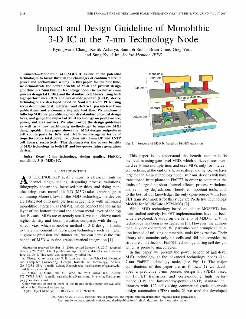
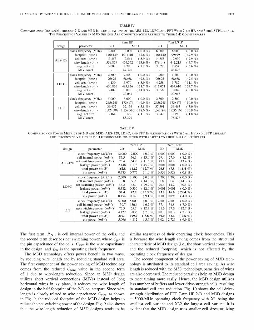
is used to derive power metrics of the implemented designs,and considering dark silicon in the advanced technologynodes [12], only 30% of sequential logics (i.e., flip-flops) areassumed to be powered ON at an instance. The toggle rate forsequential logics and primary inputs is set to 40% and 20%,respectively. Fig. 7 shows 2-D and M3D implementations ofthe benchmarks at their highest clock frequency using 7-nmHP library. Tables IV and V show the design and the powermetrics of the three benchmarks comparing M3D designs totheir 2-D counterparts, respectively.
1) Impact of Target Clock Frequency: Fig. 8 shows thetotal power saving of M3D designs compared with their2-D counterparts across target clock frequencies. Fig. 8 clearlyshows a trend that the power benefit of M3D technology isincreasing as the target clock frequency increases.
To interpret the trend, we use the following equation, whichdescribes the components of dynamic power consumption ofa design:
CHANG et al.: IMPACT AND DESIGN GUIDELINE OF MONOLITHIC 3-D IC AT THE 7-nm TECHNOLOGY NODE 2123
TABLE IV
COMPARISON OF DESIGN METRICS OF 2-D AND M3D IMPLEMENTATIONS OF THE AES-128, LDPC, AND FFT WITH 7-nm HP, AND 7-nm LSTP LIBRARY.THE PERCENTAGE VALUES IN M3D DESIGNS ARE COMPUTED WITH RESPECT TO THEIR 2-D COUNTERPARTS
TABLE V
COMPARISON OF POWER METRICS OF 2-D AND M3D, AES-128, LDPC, AND FFT IMPLEMENTATIONS WITH 7-nm HP AND LSTP LIBRARY.THE PERCENTAGE VALUES IN M3D DESIGNS ARE COMPUTED WITH RESPECT TO THEIR 2-D COUNTERPARTS
The first term, PINT, is cell internal power of the cells, andthe second term describes net switching power, where Cpin isthe pin capacitance of the cells, Cwire is the wire capacitancein the design, and fclk is the operating clock frequency.
The M3D technology offers power benefit in two ways,by reducing wire length and by reducing standard cell area.The first component of the power saving of M3D technologycomes from the reduced Cwire value in the second termof 1 due to wire-length reduction. Since an M3D designutilizes short vertical connections (MIVs) instead of longhorizontal wires in xy plane, it reduces the wire length ofdesign in the half footprint of the 2-D counterpart. Since wirelength is closely related to wire capacitance Cwire, as shownin Fig. 9, the reduced footprint of the M3D design helps toreduce the net switching power of the design. Fig. 9 also showsthat the wire-length reduction of M3D designs tends to be
similar regardless of their operating clock frequencies. Thisis because the wire length saving comes from the structuralcharacteristic of M3D design (i.e., the short vertical connectionand the reduced footprint), which is not affected by theoperating clock frequency of designs.
The second component of the power saving of M3D tech-nology is attributed to its standard cell area saving. As wirelength is reduced with the M3D technology, parasitics of wiresare also decreased. The reduced parasitics help an M3D designto meet timing more easily. Hence, the M3D design utilizesless number of buffers and lower drive-strength cells, resultingin standard cell area reduction. Fig. 10 shows the cell drive-strength distribution of FFT 7-nm HP 2-D and M3D designsat 5000-MHz operating clock frequency with X1 being thesmallest cell variant and X32 the largest cell variant. It isevident that the M3D design uses smaller cell sizes, utilizing
2124 IEEE TRANSACTIONS ON VERY LARGE SCALE INTEGRATION (VLSI) SYSTEMS, VOL. 25, NO. 7, JULY 2017
Fig. 9. Wire length and the corresponding wire capacitance saving ofAES-128, LDPC, and FFT M3D designs utilizing 7-nm HP library.
Fig. 10. Cell drive-strength distribution of FFT 7-nm HP 2-D and M3Dimplementations. Values are normalized to each cell variant of 2-D design.
more cells with X1 drive-strength cells, instead of using otherlarger variants. The standard cell area saving helps to reduceboth the first term, PINT, and the second term by reducing Cpinin 1. Fig. 11 shows the high correlation between standard cellarea and pin capacitance of a design. Another trend to notein the figure is that unlike wire-length saving, the standardcell area saving is increasing as operating clock frequencyincreases. This is because 2-D designs utilize more buffersand higher drive-strength cells to meet timing especially inhigh operating clock frequency, whereas M3D designs meettiming with lesser number of buffers and lower drive-strengthcells due to wire-length saving.
2) Impact of Characteristic of Benchmarks: We observe thesignificant difference in total power saving between LDPCand other benchmarks, as shown in Fig. 8. While the totalpower saving of AES-128 and FFT M3D designs ranges from2.18% to 12.65%, LDPC M3D designs show 23.57%–28.59%power saving depending on their operating clock frequency.To explain the difference, we rewrite 1 as follows:
Pdyn = PINT + α · Cpin · VDD2 · fclk
+α · Cwire · VDD2 · fclk. (2)
Fig. 11. Standard cell area and pin capacitance saving of M3D in AES-128,LDPC, and FFT 7-nm HP designs.
First, we observe that the ratio of the net switching power tothe cell internal power of LDPC 7-nm HP 2-D design (4.27)is much higher than the other two designs (AES-128: 0.84 andFFT: 0.54) in Table V, which means that the first term is muchsmaller than the other two terms in 2 in the LDPC design.
In addition, from Table IV, we observe that the ratio of wirelength to standard cell area of LDPC designs is 150.74 μm−1,which is also much higher than AES-128 (40.43 μm−1) andFFT (36.10 μm−1) designs. Hence, the ratio of Cwire to Cpin ismuch larger in LDPC designs than that in the other twobenchmarks, since Cpin and Cwire are highly correlated withstandard cell area and wire length of a design, respectively.
Considering that the standard cell area saving reduces thefirst two terms in 2, and the wire-length saving reduces the lastterm, we conclude that the total power saving of LDPC designsheavily depends on the wire-length saving of the design ratherthan the standard cell area saving.
Moreover, the M3D technology achieves more wire-lengthsaving in LDPC than other two benchmarks. We observe thatthe ratio of wirelength to the footprint in an LDPC 7-nm HP2-D design (69.17 μm−1) is also larger than the other twodesigns (AES-128: 27.74 μm−1 and FFT: 23.73 μm−1). Thismetric along with the average net size in Table IV indicate thatwires are more congested in LDPC. Since an M3D designhelps reduce the wire congestion by utilizing both top andbottom metal layers, it effectively reduces wire length in LDPCdesigns. By comparing Fig. 7(c) and (d), we see the efficacyof M3D technology in reducing wire congestion of the design.
3) Impact of Cell Library: The trend difference between7-nm HP and 7-nm LSTP designs can also be explained bythe ratio of Cwire to Cpin in 2. Note that the wire parasiticsof both libraries are remained the same, because they sharethe same metal layer configuration. Considering the fact thatpin capacitance of 7-nm HP library cells tend to be higherthan that of 7-nm LSTP library cells due to higher parasiticsin HP devices, the ratio of the third term in 2 to the totaldynamic power is larger in 7-nm LSTP designs than in 7-nmHP designs. This indicates that the designs with LSTP library
CHANG et al.: IMPACT AND DESIGN GUIDELINE OF MONOLITHIC 3-D IC AT THE 7-nm TECHNOLOGY NODE 2125
Fig. 12. Impact of bin size selection on the total power saving of theM3D design over the 2-D design for AES-128 at 12 GHz, LDPC at 2.5 GHz,and FFT at 5 GHz implemented with the 7-nm HP library.
cells take more advantage from wire-length saving ofM3D technology than those using HP library cells. SinceM3D designs reduce the wire length more effectively inLDPC compared with other two benchmarks as discussed inSection III-B2, we observe the largest total power saving inLDPC 7-nm LSTP M3D designs than others.
IV. M3D DESIGN SPACE EXPLORATION
Since the design quality of an M3D design heavily dependson the tier partitioning methodology of the M3D designflow described in Section III-A, we perform design spaceexploration on the tier partitioning scheme, specifically on binsize selection and clock tree partitioning.
A. Bin Size Selection
As described in Section III-A, in order to partition cellsinto two tiers, a shrunk 2-D design is, first, divided intomultiple square bins on xy plane, and area-balanced min-cutpartitioning algorithm is performed for each bin.
The impact of the bin size on the total power savingof M3D designs over 2-D designs is shown in Fig. 12.For each benchmark, twelve M3D designs are implementedfrom a shrunk 2-D design using different bin sizes, and thepower consumption of the resulting M3D designs is comparedwith the 2-D design. Fig. 12 shows that the total powersaving of all three benchmarks is maximum at the bin sizeof 3–4 μm, and the total power saving is ranged from 8.4% to12.7% for AES-128 design depending on the bin size. Anotherimportant trend to note is that unlike LDPC and FFT M3Ddesigns, the total power saving of AES-128 M3D designssharply decreases after a 5-μm bin size.
Considering that cell count and drive strength of cells arenot changed during tier partitioning step (they are determinedand fixed while implementing the shrunk 2-D design), thisdifference on the total power saving comes mainly from thewire-length saving due to the bin size selection, which showsa similar trend, as shown in Fig. 13.
Fig. 14 explains the reason why the bin size selectionaffects the wire-length saving of an M3D design. If the bin
Fig. 13. Impact of bin size during tier partitioning on wire-length savingof 7-nm HP designs.
Fig. 14. Two extreme cases showing the impact of the bin size on theM3D design quality. (a) Shrunk 2-D design with only one huge bin afterscaling cells up to their original size and (b) corresponding partitioning result.(c) Shrunk 2-D design with very small sized bins and (d) correspondingpartition result. Dashed lines and red arrows indicate bins and cell movementduring legalization, respectively.
size during tier partitioning is more than 5 μm (i.e., largebin size), area-balanced min-cut partitioning algorithm findsglobal optimal solution more easily, minimizing the numberof connections between two tiers. However, neighboring cellsin the local area tend to be clustered and placed on a singletier altogether, since cells with a global connection are morelikely to be partitioned in this case, remaining overlap betweencells even after tier partitioning. This overlap increases cellmovement while legalizing cells [red arrows in Fig. 14(b)],resulting in wire-length overhead. The local cell clustering dueto large bin size becomes more severe if a design has clustereddesign structure as AES-128 in Fig. 15(a), which indicatesthat the design has the large number of local wires, butvery few global wires. This is because while the partitioningalgorithm partitions very few global connections, the clusteredneighboring cells in the local area tend to be placed on asingle tier altogether, increasing wire-length overhead duringcell legalization.
On the other hand, in the case of bin size less than 3 um (i.e.,small bin size), it does not suffer from overlap after tierpartitioning because of its fine-grained partitioning schemeas shown in Fig. 14(c) and (d), but it is more likely to fall
2126 IEEE TRANSACTIONS ON VERY LARGE SCALE INTEGRATION (VLSI) SYSTEMS, VOL. 25, NO. 7, JULY 2017
Fig. 15. Comparison of cell placement of (a) AES-128 and (b) FFT shrunk2-D designs. AES-128 has clustered design structure, while FFT has evenlydistributed cell placement.
Fig. 16. Fixed cells and cells which are free to partition when LOF = 2.Note that the root of a clock tree, the clock source, is always placed on thetop tier.
into local optimal solution during tier partitioning, splittingunnecessarily large number of local interconnects into twotiers, showing the sharp decrease in wire-length saving of M3Ddesigns at the small bin sizes in Fig. 13.
B. Clock Tree Partitioning Methodology
In this section, two clock tree partitioning methodologies,level-of-freedom (LOF)-based partitioning [13] and prioritizedclock tree partitioning, to improve the clock tree of an M3Ddesign are presented. As discussed in Section III-A, x − ylocation of clock cells in an M3D design, including clockbuffers and flip-flops, is first determined during implementingits shrunk 2-D design. Then, during the tier partitioning step,z-location of each clock cells is determined depending on theclock tree partitioning methodology.
1) Level-of-Freedom-Based Partitioning: We define theLOF of clock cells as the distance from leaf nodes of aclock tree, and clock cells within the distance are free to bepartitioned either bottom or top tier, as shown in Fig. 16. Allother cells whose distance is larger than the LOF are fixed onone of the tiers (e.g., top tier) before partitioning. For example,if LOF = 1, only leaf cells of a clock tree (i.e., flip-flops),and the clock buffers that drive the leaf cells are free to bepartitioned on either tiers, and every other clock cells are fixedon the top tier before partitioning.
Table VI shows the number of clock cells fixed to the toptier before tier partitioning depending on LOF and the resultingnumber of clock MIVs. Since clock MIVs are used when a
TABLE VI
NUMBER OF THE FIXED CLOCK CELLS FOR EACH LOF AND THERESULTING CLOCK MIVs OF THE BENCHMARK DESIGNS
IMPLEMENTED WITH 7-nm HP LIBRARY
Fig. 17. Clock trees on the top tier span from the root of the clock tree tothe first MIV encountered along the branches of AES-128 7-nm HP designwhen (a) LOF = 1 and (b) LOF = max.
Fig. 18. Impact of LOF on the clock switching power saving of 7-nm HPM3D designs.
parent cell in a clock tree is assigned to the different tierfrom its child cell, the number of clock MIVs is increasingas LOF increases. Fig. 17 compares the clock trees on thetop tier, which span from their root of the clock tree to thefirst MIV encountered along the branches when LOF = 1 andLOF = max. Fig. 17 clearly shows that the clock tree spanningfrom the clock source is larger as LOF decreases, since morenumber of clock cells are fixed on to the top tier with low LOF.
Fig. 18 shows the impact of LOF on clock switching powersaving of M3D designs over the corresponding 2-D designs,showing that clock switching power saving decreases as LOF
CHANG et al.: IMPACT AND DESIGN GUIDELINE OF MONOLITHIC 3-D IC AT THE 7-nm TECHNOLOGY NODE 2127
Fig. 19. Clock skew of 7-nm HP M3D designs depending on LOF inLOF-based partitioning.
Fig. 20. Example comparing clock trees partitioned with (a) low LOF and(b) high LOF, showing that the extra wire (yellow wires) is required to connectclock cells on different tiers.
increases. However, total power consumption of the designsdoes not vary by a large magnitude, since the clock powerconsumption is less than 3% of the total power consumptionfor all benchmarks. On the other hand, the clock skew of thedesigns is significantly affected by LOF, as shown in Fig. 19.
The decreased clock switching power saving and theincreased clock skew in an M3D design with high LOF areattributed to the increased clock wire length of the design.As LOF affects only on the tier assignment of clock cells(i.e., z-location), not on x − y location of the cells, if LOFincreases, the number of connection crossing the tiers isincreasing, which, in turn, requires extra wires to establishthe connection, as shown Fig. 20 (yellow wires). These extrawires differentiate clock delay at the clock sink of eachbranch, hence, increasing the clock skew of the M3D design.In addition, they also increase the parasitics of the clock tree,which increases the clock switching power consumption of thedesign.
2) Prioritized Clock Tree Partitioning: In this section,we propose prioritized clock tree partitioning methodology inorder to further improve the quality of the clock tree of anM3D design. In the proposed methodology, a tier partitioningstage is divided into two phases, clock cell pretier partition-
Fig. 21. Proposed gate-level M3D design flow with prioritized clock treepartitioning to improve the clock tree of a design.
ing phase and regular cell tier partitioning phase, as shownin Fig. 21. The entire clock tree of a design, which includesclock buffers as well as flip-flops, is first partitioned into twotiers using the area-balanced min-cut partitioning algorithm.The partitioned clock cells are fixed on the assigned tier andare not changed thereafter. Then, regular cells are partitioned,so that the cell area of the top and bottom tiers is balanced.
Different from LOF-based partitioning with LOF = max,which treats clock cells as regular cells and partitions all cellsat the same time, the proposed methodology gives clock cellshigher priority over regular cells while balancing the area ofclock cells on the top and the bottom tiers.
As discussed in Section IV-B1, in order to minimize theclock skew and the clock switching power of an M3D design,it is important to reduce the number of connection betweenclock cells crossing tiers. Therefore, in clock cell pretierpartitioning phase of the proposed methodology, larger binsize is utilized for clock cells, compared with the bin sizewhich would be used for regular cells, to minimize the cutsize of the clock tree during area-balanced min-cut partitioningalgorithm. The larger bin size may cluster neighboring clockcells in local area and place all of them onto one tier, as shownin Fig. 14(b). However, considering that the number of clockcells is small compared with total cell count of a design,the issue is automatically resolved during partitioning regularcells in the next phase by placing more regular cells on theother tiers. In this paper, the bin size for clock cell pretierpartitioning is determined to be maximum in the range thatregular cell tier partition is able to balance standard cell areabetween two tiers.
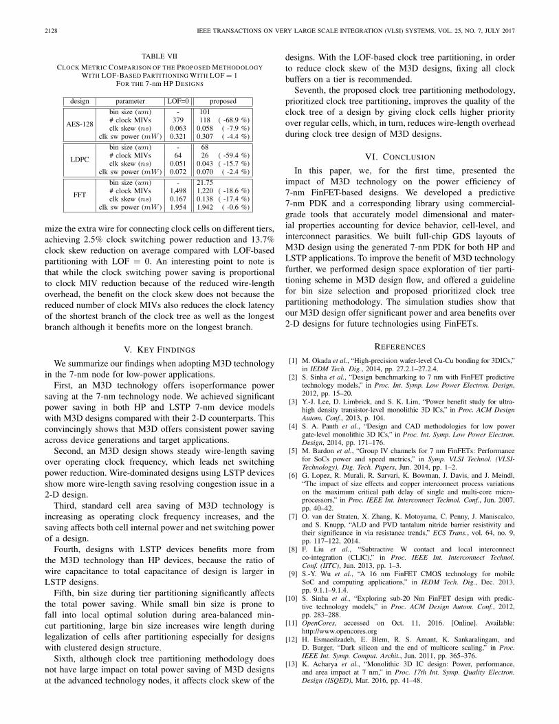
Table VII shows the bin size used for clock cell pretierpartitioning, and compares the design and power metric of theproposed methodology with those with LOF-based partitioningwith LOF = 0, which shows the best clock skew and clockswitching power saving in Section IV-B1. The bin size used forclock cell pretier partitioning phase for AES-128 and LDPC7-nm HP designs is set to be the same as entire design size(i.e., single bin for entire design). On the other hand, the binsize for FFT 7-nm HP design, which has higher clock celldensity compared with other two benchmarks, is set to 1/8 ofentire design size (i.e., 64 bins for entire design), since binsize larger than that clusters too many clock cells and placethem into single tier, leading highly imbalanced clock cell areabetween tiers in local area, which cannot be resolved in regularcell tier partitioning phase.
As shown in Table VII, the proposed methodology success-fully reduces the number of clock MIVs by finding globaloptima with a large bin size. The reduced clock MIVs mini-
2128 IEEE TRANSACTIONS ON VERY LARGE SCALE INTEGRATION (VLSI) SYSTEMS, VOL. 25, NO. 7, JULY 2017
TABLE VII
CLOCK METRIC COMPARISON OF THE PROPOSED METHODOLOGYWITH LOF-BASED PARTITIONING WITH LOF = 1
FOR THE 7-nm HP DESIGNS
mize the extra wire for connecting clock cells on different tiers,achieving 2.5% clock switching power reduction and 13.7%clock skew reduction on average compared with LOF-basedpartitioning with LOF = 0. An interesting point to note isthat while the clock switching power saving is proportionalto clock MIV reduction because of the reduced wire-lengthoverhead, the benefit on the clock skew does not because thereduced number of clock MIVs also reduces the clock latencyof the shortest branch of the clock tree as well as the longestbranch although it benefits more on the longest branch.
V. KEY FINDINGS
We summarize our findings when adopting M3D technologyin the 7-nm node for low-power applications.
First, an M3D technology offers isoperformance powersaving at the 7-nm technology node. We achieved significantpower saving in both HP and LSTP 7-nm device modelswith M3D designs compared with their 2-D counterparts. Thisconvincingly shows that M3D offers consistent power savingacross device generations and target applications.
Second, an M3D design shows steady wire-length savingover operating clock frequency, which leads net switchingpower reduction. Wire-dominated designs using LSTP devicesshow more wire-length saving resolving congestion issue in a2-D design.
Third, standard cell area saving of M3D technology isincreasing as operating clock frequency increases, and thesaving affects both cell internal power and net switching powerof a design.
Fourth, designs with LSTP devices benefits more fromthe M3D technology than HP devices, because the ratio ofwire capacitance to total capacitance of design is larger inLSTP designs.
Fifth, bin size during tier partitioning significantly affectsthe total power saving. While small bin size is prone tofall into local optimal solution during area-balanced min-cut partitioning, large bin size increases wire length duringlegalization of cells after partitioning especially for designswith clustered design structure.
Sixth, although clock tree partitioning methodology doesnot have large impact on total power saving of M3D designsat the advanced technology nodes, it affects clock skew of the
designs. With the LOF-based clock tree partitioning, in orderto reduce clock skew of the M3D designs, fixing all clockbuffers on a tier is recommended.
Seventh, the proposed clock tree partitioning methodology,prioritized clock tree partitioning, improves the quality of theclock tree of a design by giving clock cells higher priorityover regular cells, which, in turn, reduces wire-length overheadduring clock tree design of M3D designs.
VI. CONCLUSION
In this paper, we, for the first time, presented theimpact of M3D technology on the power efficiency of7-nm FinFET-based designs. We developed a predictive7-nm PDK and a corresponding library using commercial-grade tools that accurately model dimensional and mater-ial properties accounting for device behavior, cell-level, andinterconnect parasitics. We built full-chip GDS layouts ofM3D design using the generated 7-nm PDK for both HP andLSTP applications. To improve the benefit of M3D technologyfurther, we performed design space exploration of tier parti-tioning scheme in M3D design flow, and offered a guidelinefor bin size selection and proposed prioritized clock treepartitioning methodology. The simulation studies show thatour M3D design offer significant power and area benefits over2-D designs for future technologies using FinFETs.
REFERENCES
[1] M. Okada et al., “High-precision wafer-level Cu-Cu bonding for 3DICs,”in IEDM Tech. Dig., 2014, pp. 27.2.1–27.2.4.
[2] S. Sinha et al., “Design benchmarking to 7 nm with FinFET predictivetechnology models,” in Proc. Int. Symp. Low Power Electron. Design,2012, pp. 15–20.
[3] Y.-J. Lee, D. Limbrick, and S. K. Lim, “Power benefit study for ultra-high density transistor-level monolithic 3D ICs,” in Proc. ACM DesignAutom. Conf., 2013, p. 104.
[4] S. A. Panth et al., “Design and CAD methodologies for low powergate-level monolithic 3D ICs,” in Proc. Int. Symp. Low Power Electron.Design, 2014, pp. 171–176.
[5] M. Bardon et al., “Group IV channels for 7 nm FinFETs: Performancefor SoCs power and speed metrics,” in Symp. VLSI Technol. (VLSI-Technology), Dig. Tech. Papers, Jun. 2014, pp. 1–2.
[6] G. Lopez, R. Murali, R. Sarvari, K. Bowman, J. Davis, and J. Meindl,“The impact of size effects and copper interconnect process variationson the maximum critical path delay of single and multi-core micro-processors,” in Proc. IEEE Int. Interconnect Technol. Conf., Jun. 2007,pp. 40–42.
[7] O. van der Straten, X. Zhang, K. Motoyama, C. Penny, J. Maniscalco,and S. Knupp, “ALD and PVD tantalum nitride barrier resistivity andtheir significance in via resistance trends,” ECS Trans., vol. 64, no. 9,pp. 117–122, 2014.
[8] F. Liu et al., “Subtractive W contact and local interconnectco-integration (CLIC),” in Proc. IEEE Int. Interconnect Technol.Conf. (IITC), Jun. 2013, pp. 1–3.
[9] S.-Y. Wu et al., “A 16 nm FinFET CMOS technology for mobileSoC and computing applications,” in IEDM Tech. Dig., Dec. 2013,pp. 9.1.1–9.1.4.
[10] S. Sinha et al., “Exploring sub-20 Nm FinFET design with predic-tive technology models,” in Proc. ACM Design Autom. Conf., 2012,pp. 283–288.
[11] OpenCores, accessed on Oct. 11, 2016. [Online]. Available:http://www.opencores.org
[12] H. Esmaeilzadeh, E. Blem, R. S. Amant, K. Sankaralingam, andD. Burger, “Dark silicon and the end of multicore scaling,” in Proc.IEEE Int. Symp. Comput. Archit., Jun. 2011, pp. 365–376.
[13] K. Acharya et al., “Monolithic 3D IC design: Power, performance,and area impact at 7 nm,” in Proc. 17th Int. Symp. Quality Electron.Design (ISQED), Mar. 2016, pp. 41–48.
CHANG et al.: IMPACT AND DESIGN GUIDELINE OF MONOLITHIC 3-D IC AT THE 7-nm TECHNOLOGY NODE 2129
Kyungwook Chang received the B.S. degree inelectrical and computer engineering and the M.S.degree in electrical engineering and computer sci-ence from Seoul National University, Seoul, SouthKorea, in 2007 and 2010, respectively. He is cur-rently pursuing the Ph.D. degree with the Schoolof Electrical and Computer Engineering, GeorgiaInstitute of Technology, Atlanta, GA, USA.
His current research interests include monolithic3-D IC technology, advanced technology nodes, lowpower designs, and 3-D IC design methodology.
Kartik Acharya received the B.E. degree in elec-trical engineering from the Maharaja Sayajirao Uni-versity of Baroda, Vadodara, India, in 1999, and theM.S. degree in electrical engineering from SyracuseUniversity, Syracuse, NY, USA, in 2000. He iscurrently pursuing the Ph.D. degree with the Schoolof Electrical and Computer Engineering, GeorgiaInstitute of Technology, Atlanta, GA, USA.
He is currently a Power Grid Analysis Method-ology Engineer with IBM, Austin, TX, USA. Hiscurrent research interests include electrical analysis
for power and noise integrity, and design methodologies for advanced tech-nology nodes.
Saurabh Sinha received the B.Tech. degree inelectronics and instrumentation engineering fromthe National Institute of Technology at Rourkela,Rourkela, India, in 2006, and the M.S. and Ph.D.degrees in electrical engineering from Arizona StateUniversity, Tempe, AZ, USA, in 2008 and 2011,respectively.
He is currently a Staff Research Engineer withARM Research, Austin, TX, USA. His currentresearch interests include predictive technology,design-technology co-optimization at advanced tech-
nology nodes, and disruptive technologies, such as 3D-ICs and their impacton design.
Brian Cline received the B.S. degree in electricalengineering from The University of Texas at Austin,Austin, TX, USA, in 2004, and the M.S. and Ph.D.degrees in electrical engineering from the Universityof Michigan, Ann Arbor, MI, USA, in 2006 and2010, respectively.
From 2006 to 2010, he was a Graduate Fellowwith Semiconductor Research Corporation, Durham,NC, USA. He is currently a Principal Research Engi-neer with the ARM Research Group, Austin. Hiscurrent research interests include design technology
co-optimization, low-power circuit design, variation-aware computer aideddesign tool development, and very large-scale integration design optimizationfor high-performance and low-power designs.
Greg Yeric received the Ph.D. degree in micro-electronics from The University of Texas at Austin,Austin, TX, USA, in 1993.
He joined Advanced Products Research andDevelopment Laboratories in Embedded NonvolatileMemory Process Integration, Motorola, Austin, TX,USA, subsequently researching on technology devel-opment roles at TestChip Technologies, Plano, TX,USA, HPL Technologies, San Jose, CA, USA, andSynopsys, Mountain View, CA, USA. He is currentlyan ARM Fellow and the Director of Future Silicon
Research in ARM, Austin, where he is involved in design-technology co-optimization and predictive technology.
Sung Kyu Lim (S’94–M’00–SM’05) received theB.S., M.S., and Ph.D. degrees from the University ofCalifornia at Los Angeles, Los Angeles, CA, USA,in 1994, 1997, and 2000, respectively.
He joined the School of Electrical and Com-puter Engineering, Georgia Institute of Technology,Atlanta, GA, USA, in 2001, where he is currentlya Dan Fielder Endowed Chair Professor. He hasauthored the book Practical Problems in VLSI Phys-ical Design Automation (Springer, 2008). His currentresearch interests include modeling, architecture, and
electronic design automation (EDA) for 3-D ICs. His research on 3-D ICreliability is featured as Research Highlight in the Communication of theACM in 2014. His 3-D IC test chip published in the IEEE International Solid-State Circuits Conference in 2012, is generally considered the first multi-core3-D processor ever developed in academia.
Dr. Lim was a recipient of the National Science Foundation Faculty EarlyCareer Development (CAREER) Award in 2006. He received the Distin-guished Service Award in 2008. He received the Best Paper Awards from theIEEE Asian Test Symposium in 2012 and the IEEE International InterconnectTechnology Conference in 2014. He received the Class of 1940 Course SurveyTeaching Effectiveness Award from the Georgia Institute of Technology,in 2016. He was on the Advisory Board of the ACM Special Interest Groupon Design Automation from 2003 to 2008. He was an Associate Editor ofthe IEEE TRANSACTIONS ON VERY LARGE SCALE INTEGRATION SYSTEMSfrom 2007 to 2009. He has been an Associate Editor of the IEEE TRANS-ACTIONS ON COMPUTER-AIDED DESIGN OF INTEGRATED CIRCUITS AND
SYSTEMS since 2013. He has served on the Technical Program Committeeof several premier conferences in EDA.