+ All Categories
Home > Documents > 24-Channel, Constant-Current LED Driver w/ Global BC & … · Global Brightness Control and LED...

24-Channel, Constant-Current LED Driver w/ Global BC & … · Global Brightness Control and LED...

Date post: 05-Jun-2018
Category:
Upload: trinhcong
View: 216 times
Download: 0 times
Share this document with a friend
32
1FEATURES APPLICATIONS DESCRIPTION ¼ ¼ V CC ¼ ¼ ¼ DATA SCLK LAT BLANK ¼ R IREF Controller 3 ERROR READ ¼ SIN SCLK LAT SOUT V CC GND TLC5952 IC1 OUTR0 OUTB7 BLANK IREF V LED + V CC R IREF ¼ SIN SCLK LAT SOUT V CC GND TLC5952 ICn OUTR0 OUTB7 BLANK IREF TLC5952 www.ti.com........................................................................................................................................................................................................ SBVS129–MAY 2009 24-Channel, Constant-Current LED Driver with Global Brightness Control and LED Open-Short Detection Operating Temperature: –40°C to +85°C 2324-Channel Constant-Current Sink Output with Packages: HTSSOP-32, QFN-32 On/Off Control Current Capability: Full-Color LED Displays 35 mA for 16 Channels LED Signboards 26.2 mA for 8 Channels Global Brightness Control (BC) for Each Color Group: 7-Bit (128 Step), Three Groups The TLC5952 is a 24-channel, constant-current sink LED Power-Supply Voltage up to 15 V driver. Each channel can be turned on/off with V CC = 3.0 V to 5.5 V internal register data. The output channels are Constant-Current Accuracy: grouped into three groups of eight channels each. Each channel group has a 128-step global brightness Channel-to-Channel = ±1% control (BC) function. Both on/off data and BC are Device-to-Device = ±3% writable via a serial interface. The maximum current CMOS Logic Level I/O value of all 24 channels is set by a single external resistor. Data Transfer Rate: 35 MHz BLANK Pulse Width: 15 ns The TLC5952 has three error detection circuits: LED open detection (LOD), LED short detection (LSD), Open Load, Short Load, and Over-Temperature and a thermal error flag (TEF). The error detection is Detection read via a serial interface. Thermal Shutdown (TSD) with Auto Restart Delay Switching to Prevent Inrush Current Typical Application Circuit (Multiple Daisy-Chained TLC5952s) 1 Please be aware that an important notice concerning availability, standard warranty, and use in critical applications of Texas Instruments semiconductor products and disclaimers thereto appears at the end of this data sheet. 2PowerPAD is a trademark of Texas Instruments, Incorporated. 3All other trademarks are the property of their respective owners. UNLESS OTHERWISE NOTED this document contains Copyright © 2009, Texas Instruments Incorporated PRODUCTION DATA information current as of publication date. Products conform to specifications per the terms of Texas Instruments standard warranty. Production processing does not necessarily include testing of all parameters.
Transcript

1FEATURES

APPLICATIONS

DESCRIPTION

¼ ¼

VCC

¼ ¼

¼

DATA

SCLK

LAT

BLANK

¼

RIREF

Controller

3ERROR

READ

¼

SIN

SCLK

LAT

SOUT

VCC

GND

TLC5952

IC1

OUTR0 OUTB7

BLANK

IREF

VLED

+

VCC

RIREF

¼

SIN

SCLK

LAT

SOUT

VCC

GND

TLC5952

ICn

OUTR0 OUTB7

BLANK

IREF

TLC5952

www.ti.com........................................................................................................................................................................................................ SBVS129–MAY 2009

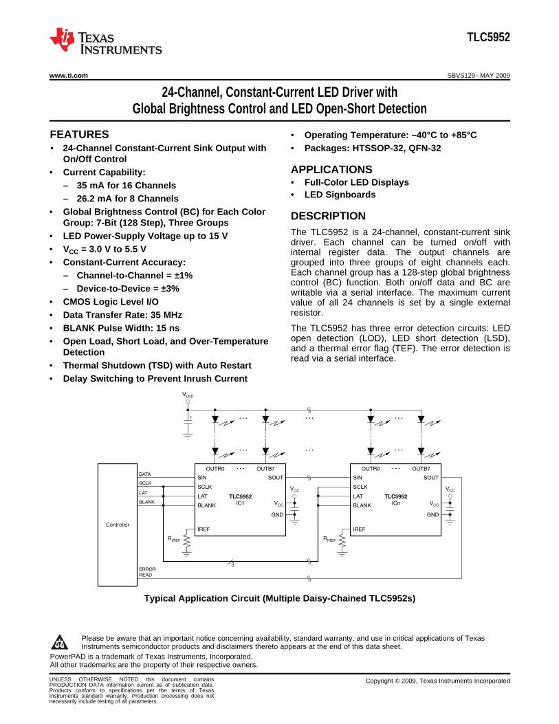
24-Channel, Constant-Current LED Driver withGlobal Brightness Control and LED Open-Short Detection

• Operating Temperature: –40°C to +85°C23• 24-Channel Constant-Current Sink Output with • Packages: HTSSOP-32, QFN-32

On/Off Control• Current Capability:

• Full-Color LED Displays– 35 mA for 16 Channels• LED Signboards– 26.2 mA for 8 Channels

• Global Brightness Control (BC) for Each ColorGroup: 7-Bit (128 Step), Three Groups

The TLC5952 is a 24-channel, constant-current sink• LED Power-Supply Voltage up to 15 Vdriver. Each channel can be turned on/off with

• VCC = 3.0 V to 5.5 V internal register data. The output channels are• Constant-Current Accuracy: grouped into three groups of eight channels each.

Each channel group has a 128-step global brightness– Channel-to-Channel = ±1%control (BC) function. Both on/off data and BC are– Device-to-Device = ±3% writable via a serial interface. The maximum current

• CMOS Logic Level I/O value of all 24 channels is set by a single externalresistor.• Data Transfer Rate: 35 MHz

• BLANK Pulse Width: 15 ns The TLC5952 has three error detection circuits: LEDopen detection (LOD), LED short detection (LSD),• Open Load, Short Load, and Over-Temperatureand a thermal error flag (TEF). The error detection isDetection read via a serial interface.

• Thermal Shutdown (TSD) with Auto Restart• Delay Switching to Prevent Inrush Current

Typical Application Circuit (Multiple Daisy-Chained TLC5952s)

1

Please be aware that an important notice concerning availability, standard warranty, and use in critical applications of TexasInstruments semiconductor products and disclaimers thereto appears at the end of this data sheet.

2PowerPAD is a trademark of Texas Instruments, Incorporated.3All other trademarks are the property of their respective owners.

UNLESS OTHERWISE NOTED this document contains Copyright © 2009, Texas Instruments IncorporatedPRODUCTION DATA information current as of publication date.Products conform to specifications per the terms of TexasInstruments standard warranty. Production processing does notnecessarily include testing of all parameters.

ABSOLUTE MAXIMUM RATINGS (1) (2)

TLC5952

SBVS129–MAY 2009........................................................................................................................................................................................................ www.ti.com

This integrated circuit can be damaged by ESD. Texas Instruments recommends that all integrated circuits be handled withappropriate precautions. Failure to observe proper handling and installation procedures can cause damage.

ESD damage can range from subtle performance degradation to complete device failure. Precision integrated circuits may be moresusceptible to damage because very small parametric changes could cause the device not to meet its published specifications.

ORDERING INFORMATION (1)

TRANSPORT MEDIA,PRODUCT PACKAGE-LEAD ORDERING NUMBER QUANTITY

TLC5952DAPR Tape and Reel, 2000TLC5952 HTSSOP-32 PowerPAD™

TLC5952DAP Tube, 46TLC5952RHBR Tape and Reel, 3000

TLC5952 5-mm × 5-mm QFN-32 (2)TLC5952RHBT Tape and Reel, 250

(1) For the most current package and ordering information see the Package Option Addendum at the end of this document, or see the TIweb site at www.ti.com.

(2) Product preview device.

Over operating free-air temperature range, unless otherwise noted.

PARAMETER TLC5952 UNITVCC Supply voltage VCC –0.3 to +6.0 V

OUTR0-OUTR7, OUTG0-OUTG7 45 mAIOUT Output current (dc)

OUTB0-OUTB7 35 mAVIN Input voltage range SIN, SCLK, LAT, BLANK, IREF –0.3 to VCC + 0.3 V

SOUT –0.3 to VCC + 0.3 VVOUT Output voltage range OUTR0-OUTR7, OUTG0-OUTG7, –0.3 to +16 VOUTB0-OUTB7TJ(max) Operation junction temperature +150 °CTSTG Storage temperature range –55 to +150 °C

Human body model (HBM) 2000 VESD rating

Charged device model (CDM) 500 V

(1) Stresses beyond those listed under absolute maximum ratings may cause permanent damage to the device. These are stress ratingsonly, and functional operation of the device at these or any other conditions beyond those indicated under recommended operatingconditions is not implied. Exposure to absolute-maximum-rated conditions for extended periods may affect device reliability.

(2) All voltage values are with respect to network ground terminal.

2 Submit Documentation Feedback Copyright © 2009, Texas Instruments Incorporated

Product Folder Link(s): TLC5952

DISSIPATION RATINGS

RECOMMENDED OPERATING CONDITIONS

TLC5952

www.ti.com........................................................................................................................................................................................................ SBVS129–MAY 2009

DERATING FACTOR TA < +25°C TA = +70°C TA = +85°CPACKAGE ABOVE TA = +25°C POWER RATING POWER RATING POWER RATING

HTSSOP-32 with 42.54 mW/°C 5318 mW 3403 mW 2765 mWPowerPAD soldered (1)

HTSSOP-32 with 22.56 mW/°C 2820 mW 1805 mW 1466 mWPowerPAD not soldered (2)

QFN-32 (3) 27.86 mW/°C 3482 mW 2228 mW 1811 mW

(1) With PowerPAD soldered onto copper area on printed circuit board (PCB); 2-oz. copper. For more information, see SLMA002 (availablefor download at www.ti.com).

(2) With PowerPAD not soldered onto copper area on PCB.(3) The package thermal impedance is calculated in accordance with JESD51-5.

At TA = –40°C to +85°C, unless otherwise noted.

TLC5952PARAMETER MIN NOM MAX UNIT

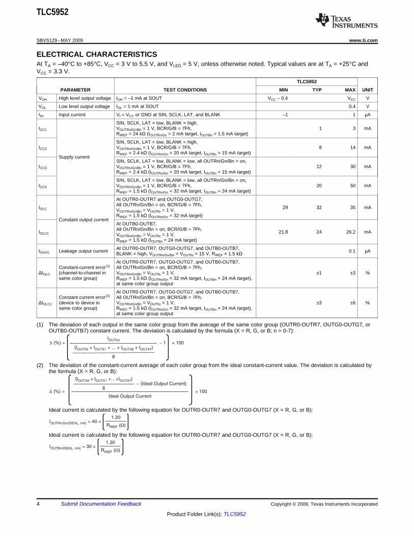
DC CHARACTERISTICS: VCC = 3 V to 5.5 VVCC Supply voltage 3.0 5.5 V

OUTR0-OUTR7, OUTG0-OUTG7,VO Voltage applied to output 15 VOUTB0-OUTB7VIH High level input voltage SIN, SCLK, LAT, BLANK 0.7 × VCC VCC VVIL Low level input voltage SIN, SCLK, LAT, BLANK GND 0.3 × VCC VIOH High level output current SOUT –1 mAIOL Low level output current SOUT 1 mA

OUTR0-OUTR7, OUTG0-OUTG7 35 mAIOLC Constant output sink current

OUTB0-OUTB7 26.2 mAOperating free-airTA –40 +85 °CtemperatureOperating junctionTJ –40 +125 °Ctemperature

AC CHARACTERISTICS, VCC = 3 V to 5.5 VfCLK (SCLK) Data shift clock frequency SCLK 35 MHzTWH0 SCLK 10 nsTWL0 SCLK 10 nsTWH1 Pulse duration LAT 15 nsTWH2 BLANK 15 nsTWL2 BLANK 15 nsTSU0 SIN – SCLK↑ 4 ns

Setup timeTSU1 LAT↑ – SCLK↑ 150 nsTH0 SIN – SCLK↑ 3 ns

Hold timeTH1 LAT↑ – SCLK↑ 10 ns

Copyright © 2009, Texas Instruments Incorporated Submit Documentation Feedback 3

Product Folder Link(s): TLC5952

ELECTRICAL CHARACTERISTICS

D (%) =IOUTXn

- 1(I + I + ... + I )OUTX0 OUTX1 OUTX6 + IOUTX7

8

´ 100

D (%) =Ideal Output Current

- (Ideal Output Current)(I + + )OUTX0 ¼I +IOUTX1 OUTX7

8´ 100

I = 40 ´OUTRn/Gn(IDEAL, mA)

1.20

R ( )WIREF

I = 30 ´OUTBn(IDEAL, mA)

1.20

R ( )WIREF

TLC5952

SBVS129–MAY 2009........................................................................................................................................................................................................ www.ti.com

At TA = –40°C to +85°C, VCC = 3 V to 5.5 V, and VLED = 5 V, unless otherwise noted. Typical values are at TA = +25°C andVCC = 3.3 V.

TLC5952

PARAMETER TEST CONDITIONS MIN TYP MAX UNIT

VOH High level output voltage IOH = –1 mA at SOUT VCC – 0.4 VCC V

VOL Low level output voltage IOL = 1 mA at SOUT 0.4 V

IIN Input current VI = VCC or GND at SIN, SCLK, LAT, and BLANK –1 1 µA

SIN, SCLK, LAT = low, BLANK = high,ICC1 VOUTRn/Gn/Bn = 1 V, BCR/G/B = 7Fh, 1 3 mA

RIREF = 24 kΩ (IOUTRn/Gn = 2 mA target, IOUTBn = 1.5 mA target)

SIN, SCLK, LAT = low, BLANK = high,ICC2 VOUTRn/Gn/Bn = 1 V, BCR/G/B = 7Fh, 8 14 mA

RIREF = 2.4 kΩ (IOUTRn/Gn = 20 mA target, IOUTBn = 15 mA target)Supply current

SIN, SCLK, LAT = low, BLANK = low, all OUTRn/Gn/Bn = on,ICC3 VOUTRn/Gn/Bn = 1 V, BCR/G/B = 7Fh, 12 30 mA

RIREF = 2.4 kΩ (IOUTRn/Gn = 20 mA target, IOUTBn = 15 mA target)

SIN, SCLK, LAT = low, BLANK = low, all OUTRn/Gn/Bn = on,ICC4 VOUTRn/Gn/Bn = 1 V, BCR/G/B = 7Fh, 20 50 mA

RIREF = 1.5 kΩ (IOUTRn/Gn = 32 mA target, IOUTBn = 24 mA target)

At OUTR0-OUTR7 and OUTG0-OUTG7,All OUTRn/Gn/Bn = on, BCR/G/B = 7Fh,IOLC 29 32 35 mAVOUTRn/Gn/Bn = VOUTfix = 1 V,RIREF = 1.5 kΩ (IOUTRn/Gn = 32 mA target)

Constant output currentAt OUTB0-OUTB7,All OUTRn/Gn/Bn = on, BCR/G/B = 7Fh,IOLC1 21.8 24 26.2 mAVOUTRn/Gn/Bn = VOUTfix = 1 V,RIREF = 1.5 kΩ (IOUTBn = 24 mA target)

At OUTR0-OUTR7, OUTG0-OUTG7, and OUTB0-OUTB7,IOLKG Leakage output current 0.1 µABLANK = high, VOUTRn/Gn/Bn = VOUTfix = 15 V, RIREF = 1.5 kΩ

At OUTR0-OUTR7, OUTG0-OUTG7, and OUTB0-OUTB7,Constant-current error (1) All OUTRn/Gn/Bn = on, BCR/G/B = 7Fh,

ΔIOLC (channel-to-channel in VOUTRn/Gn/Bn = VOUTfix = 1 V, ±1 ±3 %same color group) RIREF = 1.5 kΩ (IOUTRn/Gn = 32 mA target, IOUTBn = 24 mA target),

at same color group output

At OUTR0-OUTR7, OUTG0-OUTG7, and OUTB0-OUTB7,Constant current error (2) All OUTRn/Gn/Bn = on, BCR/G/B = 7Fh,

ΔIOLC1 (device to device in VOUTRn/Gn/Bn = VOUTfix = 1 V, ±3 ±6 %same color group) RIREF = 1.5 kΩ (IOUTRn/Gn = 32 mA target, IOUTBn = 24 mA target),

at same color group output

(1) The deviation of each output in the same color group from the average of the same color group (OUTR0-OUTR7, OUTG0-OUTG7, orOUTB0-OUTB7) constant current. The deviation is calculated by the formula (X = R, G, or B; n = 0-7):

(2) The deviation of the constant-current average of each color group from the ideal constant-current value. The deviation is calculated bythe formula (X = R, G, or B):

Ideal current is calculated by the following equation for OUTR0-OUTR7 and OUTG0-OUTG7 (X = R, G, or B):

Ideal current is calculated by the following equation for OUTR0-OUTR7 and OUTG0-OUTG7 (X = R, G, or B):

4 Submit Documentation Feedback Copyright © 2009, Texas Instruments Incorporated

Product Folder Link(s): TLC5952

100

(I at V = 3.0 V)OUTXn CC

(I at V = 5.5 V) (I at V = 3.0 V)OUTXn OUTXnCC CC-

5.5 V 3 V-

D (%/V) = ´

100

3 V 1 V-

´

(I at V = 1 V)OUTXn OUTXn

(I at V = 3 V) (I at V = 1 V)-OUTXn OUTXn OUTXn OUTXnD (%/V) =

TLC5952

www.ti.com........................................................................................................................................................................................................ SBVS129–MAY 2009

ELECTRICAL CHARACTERISTICS (continued)At TA = –40°C to +85°C, VCC = 3 V to 5.5 V, and VLED = 5 V, unless otherwise noted. Typical values are at TA = +25°C andVCC = 3.3 V.

TLC5952

PARAMETER TEST CONDITIONS MIN TYP MAX UNIT

At OUTR0-OUTR7, OUTG0-OUTG7, and OUTB0-OUTB7,ΔIOLC2 Line regulation (3) All OUTRn/Gn/Bn = on, BCR/G/B = 7Fh, ±0.5 ±1 %

VOUTRn/Gn/Bn = VOUTfix = 1 V, RIREF = 1.5 kΩ

At OUTR0-OUTR7, OUTG0-OUTG7, and OUTB0-OUTB7,ΔIOLC3 Load regulation (4) All OUTRn/Gn/Bn = on, BCR/G/B = 7Fh, ±1 ±3 %/V

VOUTRn/Gn/Bn = 1 V to 3 V, VOUTfix = 1 V, RIREF = 1.5 kΩ

Thermal error flagTTEF Junction temperature (5) +150 +165 +180 °Cthreshold

Thermal error flagTHYS Junction temperature (5) 5 10 20 °Chysteresis

VLOD0 All OUTRn/Gn/Bn = on, detection voltage select code = 0h 0.25 0.30 0.35 V

VLOD1 All OUTRn/Gn/Bn = on, detection voltage select code = 1h 0.50 0.60 0.70 VLED open detectionthresholdVLOD2 All OUTRn/Gn/Bn = on, detection voltage select code = 2h 0.80 0.90 1.00 V

VLOD3 All OUTRn/Gn/Bn = on, detection voltage select code = 3h 1.10 1.20 1.30 V

VLSD0 All OUTRn/Gn/Bn = on, detection voltage select code = 4h 0.55 × VCC 0.60 × VCC 0.65 × VCC V

VLSD1 All OUTRn/Gn/Bn = on, detection voltage select code = 5h 0.65 × VCC 0.70 × VCC 0.75 × VCC VLED short detectionthresholdVLSD2 All OUTRn/Gn/Bn = on, detection voltage select code = 6h 0.75 × VCC 0.80 × VCC 0.85 × VCC V

VLSD3 All OUTRn/Gn/Bn = on, detection voltage select code = 7h 0.85 × VCC 0.90 × VCC 0.95 × VCC V

VIREF Reference voltage output RIREF = 1.5 kΩ 1.17 1.20 1.23 V

(3) Line regulation is calculated by the following equation (X = R, G, or B; n = 0-7):

(4) Load regulation is calculated by the following equation (X = R, G, or B; n = 0-7):

(5) Not tested; specified by design.

Copyright © 2009, Texas Instruments Incorporated Submit Documentation Feedback 5

Product Folder Link(s): TLC5952

SWITCHING CHARACTERISTICS

TLC5952

SBVS129–MAY 2009........................................................................................................................................................................................................ www.ti.com

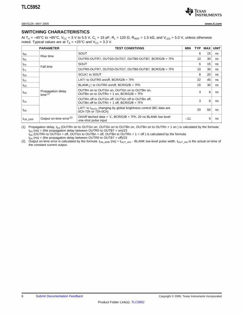
At TA = –40°C to +85°C, VCC = 3 V to 5.5 V, CL = 15 pF, RL = 120 Ω, RIREF = 1.5 kΩ, and VLED = 5.0 V, unless otherwisenoted. Typical values are at TA = +25°C and VCC = 3.3 V.

PARAMETER TEST CONDITIONS MIN TYP MAX UNITtR0 SOUT 6 15 ns

Rise timetR1 OUTR0-OUTR7, OUTG0-OUTG7, OUTB0-OUTB7, BCR/G/B = 7Fh 10 30 nstF0 SOUT 6 15 ns

Fall timetF1 OUTR0-OUTR7, OUTG0-OUTG7, OUTB0-OUTB7, BCR/G/B = 7Fh 10 30 nstD0 SCLK↑ to SOUT 8 20 nstD1 LAT↑ to OUTR0 on/off, BCR/G/B = 7Fh 22 45 nstD2 BLANK↓↑ to OUTR0 on/off, BCR/G/B = 7Fh 15 30 ns

OUTRn on to OUTGn on, OUTGn on to OUTBn on,Propagation delaytD3 3 6 nsOUTBn on to OUTRn + 1 on, BCR/G/B = 7Fhtime (1)

OUTRn off to OUTGn off, OUTGn off to OUTBn off,tD4 3 6 nsOUTBn off to OUTRn + 1 off, BCR/G/B = 7FhLAT↑ to IOUTn changing by global brightness control (BC data aretD5 20 50 ns0Ch-72h or 72h-0Ch)On/off latched data = '1', BCR/G/B = 7Fh, 20 ns BLANK low leveltON_ERR Output on-time error (2) –11 5 nsone-shot pulse input

(1) Propagation delay, tD3 (OUTRn on to OUTGn on, OUTGn on to OUTBn on, OUTBn on to OUTRn + 1 on ) is calculated by the formula:tD3 (ns) = (the propagation delay between OUTR0 to OUTB7 = on)/23tD4 (OUTRn to OUTGn = off, OUTGn to OUTBn = off, OUTBn to OUTRn + 1 = off ) is calculated by the formula:tD4 (ns) = (the propagation delay between OUTR0 to OUTB7 = off)/23

(2) Output on-time error is calculated by the formula: tON_ERR (ns) = tOUT_ON – BLANK low-level pulse width. tOUT_ON is the actual on-time ofthe constant current output.

6 Submit Documentation Feedback Copyright © 2009, Texas Instruments Incorporated

Product Folder Link(s): TLC5952

FUNCTIONAL BLOCK DIAGRAM

1-Bit TEF Data

3

8 Channels

Constant-Current

Sink Driver

Control Data Latch

(Three Groups, 7-Bit Global Brightness Control

LOD/LSD Voltage and Detection Type Select)

24

24

24

24

MSB

SIN

Common Shift Register

Output On/Off Data Latch

OUTR0

VCC

Reference

Current

Control

16 Channels

Constant-Current Sink Driver

LED Open Detection (LOD)/LED Short Detection (LSD)

21

LSB

LSB MSB

0 24

0 23

LSB MSB

0 23

Thermal

Detector

LOD/LSD

Holder

24

On/Off Control with Output Delay

24

7-Bit Global

Brightness

Control

8167 7 7

Detection

Voltage

Bit 24

24-Bit LOD or 24-Bit LSD Data

TEF

Holder

LAT

BLANK

IREF

GND

OUTR7 OUTG0 OUTG7 OUTB0 OUTB7

VCC

SOUT

SCLK

¼ ¼ ¼

¼ ¼ ¼

7-Bit Global

Brightness

Control

7-Bit Global

Brightness

Control

TLC5952

www.ti.com........................................................................................................................................................................................................ SBVS129–MAY 2009

Copyright © 2009, Texas Instruments Incorporated Submit Documentation Feedback 7

Product Folder Link(s): TLC5952

PIN CONFIGURATIONS

LAT

SCLK

SIN

GND

IREF

VCC

SOUT

BLANK

24

23

22

21

20

19

18

17

OUTB2

OUTR3

OUTG3

OUTB3

OUTR4

OUTG4

OUTB4

OUTR5

1

2

3

4

5

6

7

8

Thermal Pad

(Bottom Side)

OU

TR

025

OU

TG

026

OU

TB

027

OU

TR

128

OU

TG

129

OU

TB

130

OU

TR

231

OU

TG

232

OU

TG

59

OU

TB

716

OU

TG

715

OU

TR

714

OU

TB

613

OU

TG

612

OU

TR

611

OU

TB

510

Thermal Pad

(Bottom Side)

GND

SIN

SCLK

LAT

OUTR0

OUTG0

OUTB0

OUTR1

OUTG1

OUTB1

OUTR2

OUTG2

1

2

3

4

5

6

7

8

9

10

11

12

13

14

OUTB2

OUTR3

15

16

OUTG3

OUTB3

BLANK

OUTB7

OUTG7

OUTR7

OUTB6

OUTG6

OUTR6

OUTB5

OUTG5

OUTR5

OUTB4

OUTG4

OUTR4

25

24

23

22

21

20

19

18

17

29

28

27

26

IREF32

VCC31

SOUT30

TLC5952

SBVS129–MAY 2009........................................................................................................................................................................................................ www.ti.com

DAP PACKAGE RHB PACKAGE(1)HTSSOP-32 PowerPAD 5 mm × 5 mm QFN-32

(TOP VIEW) (TOP VIEW)

(1) Product preview device.

8 Submit Documentation Feedback Copyright © 2009, Texas Instruments Incorporated

Product Folder Link(s): TLC5952

TLC5952

www.ti.com........................................................................................................................................................................................................ SBVS129–MAY 2009

TERMINAL FUNCTIONSTERMINAL

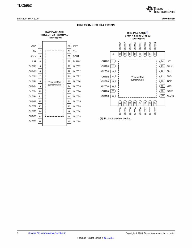
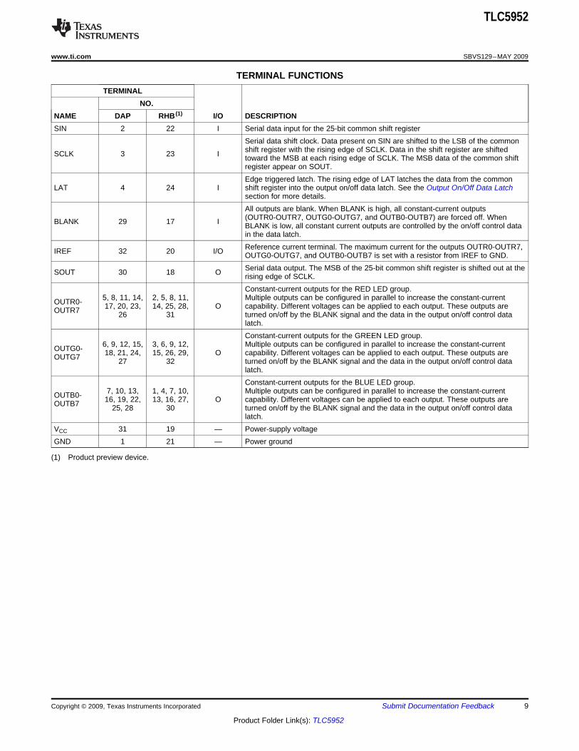
NO.NAME DAP RHB (1) I/O DESCRIPTIONSIN 2 22 I Serial data input for the 25-bit common shift register

Serial data shift clock. Data present on SIN are shifted to the LSB of the commonshift register with the rising edge of SCLK. Data in the shift register are shiftedSCLK 3 23 I toward the MSB at each rising edge of SCLK. The MSB data of the common shiftregister appear on SOUT.Edge triggered latch. The rising edge of LAT latches the data from the common

LAT 4 24 I shift register into the output on/off data latch. See the Output On/Off Data Latchsection for more details.All outputs are blank. When BLANK is high, all constant-current outputs(OUTR0-OUTR7, OUTG0-OUTG7, and OUTB0-OUTB7) are forced off. WhenBLANK 29 17 I BLANK is low, all constant current outputs are controlled by the on/off control datain the data latch.Reference current terminal. The maximum current for the outputs OUTR0-OUTR7,IREF 32 20 I/O OUTG0-OUTG7, and OUTB0-OUTB7 is set with a resistor from IREF to GND.Serial data output. The MSB of the 25-bit common shift register is shifted out at theSOUT 30 18 O rising edge of SCLK.Constant-current outputs for the RED LED group.

5, 8, 11, 14, 2, 5, 8, 11, Multiple outputs can be configured in parallel to increase the constant-currentOUTR0- 17, 20, 23, 14, 25, 28, O capability. Different voltages can be applied to each output. These outputs areOUTR7 26 31 turned on/off by the BLANK signal and the data in the output on/off control datalatch.Constant-current outputs for the GREEN LED group.

6, 9, 12, 15, 3, 6, 9, 12, Multiple outputs can be configured in parallel to increase the constant-currentOUTG0- 18, 21, 24, 15, 26, 29, O capability. Different voltages can be applied to each output. These outputs areOUTG7 27 32 turned on/off by the BLANK signal and the data in the output on/off control datalatch.Constant-current outputs for the BLUE LED group.

7, 10, 13, 1, 4, 7, 10, Multiple outputs can be configured in parallel to increase the constant-currentOUTB0- 16, 19, 22, 13, 16, 27, O capability. Different voltages can be applied to each output. These outputs areOUTB7 25, 28 30 turned on/off by the BLANK signal and the data in the output on/off control datalatch.

VCC 31 19 — Power-supply voltageGND 1 21 — Power ground

(1) Product preview device.

Copyright © 2009, Texas Instruments Incorporated Submit Documentation Feedback 9

Product Folder Link(s): TLC5952

PARAMETER MEASUREMENT INFORMATION

PIN EQUIVALENT INPUT AND OUTPUT SCHEMATIC DIAGRAMSVCC

INPUT

GND

VCC

SOUT

GND

OUTn

GND

TEST CIRCUITS

VCC

VCC

GND

IREF OUTXn(2)

RIREF

RL

CL

(1)VLED VCC

VCC

GND

SOUT

CL

(1)

¼¼

VCC

RIREF

VOUTfix

VOUTRn/Gn/Bn

OUTR0VCC

OUTXn(1)

OUTB7GND

IREF

TLC5952

SBVS129–MAY 2009........................................................................................................................................................................................................ www.ti.com

Figure 1. SIN, SCLK, LAT, BLANK Figure 2. SOUT

Figure 3. OUTR0/G0/B0 Through OUTR7/G7/B7

(1) CL includes measurement probe and jig capacitance. (1) CL includes measurement probe and jig capacitance.(2) X = R, G, or B; n = 0-7.

Figure 5. Rise Time and Fall Time Test Circuit for SOUTFigure 4. Rise Time and Fall Time Test Circuit for

OUTRn/Gn/Bn

(1) X = R, G, or B; n = 0-7.

Figure 6. Constant-Current Test Circuit for OUTRn/Gn/Bn

10 Submit Documentation Feedback Copyright © 2009, Texas Instruments Incorporated

Product Folder Link(s): TLC5952

TIMING DIAGRAMST , T, T , T , T :WH0 WH1WL0 WH2 WL2

INPUT

CLOCK

INPUT(1)

DATA/CONTROL

INPUT(1)

T , T T , T, :SU0 SU1 H0 H1

TSU TH

VCC

VCC

GND

VCC

GND

GND

50%

50%

50%

TWH TWL

t , t , t , t , t , t , t :, t , t , tR0 R1 F0 F1 D0 D1 D2 D3 D4 D5

INPUT(1) 50%

50%

90%

10%

OUTPUT

tD

t or tR F

V or VOL OUTRn/Gn/BnL

V or VOH OUTRn/Gn/BnH

GND

VCC

TLC5952

www.ti.com........................................................................................................................................................................................................ SBVS129–MAY 2009

(1) Input pulse rise and fall time is 1 ns to 3 ns.

Figure 7. Input Timing

(1) Input pulse rise and fall time is 1 ns to 3 ns.

Figure 8. Output Timing

Copyright © 2009, Texas Instruments Incorporated Submit Documentation Feedback 11

Product Folder Link(s): TLC5952

¼ ¼ ¼ ¼

¼ ¼ ¼ ¼

Current Data

tD5

tD0

SOUT

(Common Shift Register Bit 24)

R0B

On

G0B

On

B7B

On

LOD

B7B

LOD

G0B

LOD

R0B

tF1

High

23

Cont

0

Cont

LOD

G7B

23

Cont

LOD

R0B

1

Cont

tD3

tD3

tD3

tD4

tR1

TEF

B

LOD

R0A

23

ContHighB7B

OnLow

0A

On

LowLOD

B7B

TEF

A

SCLK

SIN

OUTR0 ON

OFF

1 2 3 4 5 6

LAT

On/Off Data Latch

(Internal)

BLANK

ON

OFF

ON

OFF

ON

OFF

TWH0

TWL0

TSU0

TH0

f

(SCLK)CLK

t /tR0 F0

23 24 25

G7B

On

R7B

On

B6B

On

R0B

On

G0B

On

B0B

On

R6B

On

22

Cont

21

Cont

0

Cont

LOD

G7A

LOD

R7A

LOD

B6A

LOD

G6A

LOD

R6A

LOD

G0A

LOD

G7B

LOD

R7B

LOD

G0B

LOD

R0B

LOD

B7A

1 2 3 23 24 25

Previous Data Current Data

1

Cont

(V )OUTRn/Gn/BnH

(V )OUTRn/Gn/BnL

Control Data Latch

(Internal)Previous Data

OUTG0

OUTB0

OUTR1

OUTR7 ON

OFF

ON

OFF

ON

OFF

OUTG7

OUTB7

Common Shift Register

Bit 0 (Internal)23

ContHighB7B

OnLow

G7B

On

R7B

On

B6B

On

G0B

On

B0B

On

22

Cont

2

Cont

Common Shift Register

Bit 1 (Internal)HighLow

B7B

On

G7B

On

R7B

On

B0B

On

R1B

On

3

Cont

1

Cont

2

Cont

Common Shift Register

Bit 23 (Internal)Low

tD2

LOD

R0A

LOD

G7A

LOD

R7A

LOD

B6A

LOD

G6A

LOD

B7A

LOD

R6A

LOD

R0A

LOD

G0A

LOD

R7B

LOD

B6B

LOD

G0B

LOD

R0B

tD4

tD4

tD2 tD1

Output On/Off Data Write Control Data Write

G6B

On

G6B

On

B6B

On

LOD

B5A

Output current

is changed

by BC data.

2

Cont

TH1 TWH1

TSU1

TWH2TWL2

RED outputs are turned off by output on/off data.

TLC5952

SBVS129–MAY 2009........................................................................................................................................................................................................ www.ti.com

TIMING DIAGRAMS (continued)

Figure 9. Timing Diagram

12 Submit Documentation Feedback Copyright © 2009, Texas Instruments Incorporated

Product Folder Link(s): TLC5952

TYPICAL CHARACTERISTICS

100

10

10 20 30 35

Output Current (mA)

R, R

efe

rence R

esis

tor

(k)

W

IRE

F

25

3200

1920

1371

9600

4800

2400

1600

155 10

24000

100

10

10 20 30 35

Output Current (mA)

R, R

efe

rence R

esis

tor

(k)

W

IRE

F

25

1800 13741440

155 10

24000

18000

7200

2400

3600

6000

5000

4000

3000

2000

1000

0-40 -20 80 100

Free-Air Temperature ( C)°

Pow

er

Dis

sip

ation R

ate

(m

W)

0 20 40 60

TLC5952DAP

PowerPAD Soldered

TLC5952RHB

TLC5952DAP

PowerPAD Not Soldered

40

35

30

25

20

15

10

5

00 1.0 3.0

Output Voltage (V)

Outp

ut C

urr

ent (m

A)

2.00.5 2.51.5

T = +25 C, V = 3.3 V, BCR/G = 7Fh° CCA I = 35 mAO

I = 30 mAO

I = 20 mAO

I = 10 mAO

I = 5 mAOI = 2 mAO

40

35

30

25

20

15

10

5

00 1.0 3.0

Output Voltage (V)

Outp

ut C

urr

ent (m

A)

2.00.5 2.51.5

T = +25 C

V = 3.3 V

BCB = 7Fh

°A

CC

I = 26.2 mAO

I = 22.5 mAO I = 15 mAO

I = 7.5 mAOI = 1.5 mAOI = 3.75 mAO

40

35

30

25

20

15

10

5

00 1.0 3.0

Output Voltage (V)

Outp

ut C

urr

ent (m

A)

2.00.5 2.51.5

I = 35 mAO

I = 30 mAO

I = 20 mAO

I = 10 mAO

I = 2 mAO I = 5 mAO

T = +25 C, V = 5 V, BCR/G = 7Fh° CCA

TLC5952

www.ti.com........................................................................................................................................................................................................ SBVS129–MAY 2009

At TA = +25°C and VCC = 3.3 V, unless otherwise noted.

REFERENCE RESISTOR vs OUTPUT CURRENT REFERENCE RESISTOR vs OUTPUT CURRENT(RED and GREEN Color Group) (BLUE Color Group)

Figure 10. Figure 11.

OUTPUT CURRENT vs OUTPUT VOLTAGEPOWER DISSIPATION RATE (RED and GREEN Color Group)

Figure 12. Figure 13.

OUTPUT CURRENT vs OUTPUT VOLTAGE OUTPUT CURRENT vs OUTPUT VOLTAGE(BLUE Color Group) (RED and GREEN Color Group)

Figure 14. Figure 15.

Copyright © 2009, Texas Instruments Incorporated Submit Documentation Feedback 13

Product Folder Link(s): TLC5952

40

35

30

25

20

15

10

5

00 1.0 3.0

Output Voltage (V)

Outp

ut C

urr

ent (m

A)

2.00.5 2.51.5

T = +25 C

V = 5 V

BCB = 7Fh

°A

CC

I = 26.2 mAO

I = 22.5 mAO I = 15 mAO

I = 7.5 mAOI = 1.5 mAOI = 3.75 mAO

40

39

38

37

36

35

34

33

32

31

300 1.0 3.0

Output Voltage (V)

Outp

ut C

urr

ent (m

A)

2.00.5 2.51.5

I = 35 mA

V = 3.3 V

BCR/G = 7Fh

OLCMax

CC

T = 40 CA - °

T = +25 CA °

T = +85 CA °

31

30

29

28

27

26

25

24

23

22

210 1.0 3.0

Output Voltage (V)

Outp

ut C

urr

ent (m

A)

2.00.5 2.51.5

I = 26.2 mA

V = 3.3 V

BCB = 7Fh

OLCMax

CC

T = 40 CA - °

T = +25 CA °

T = +85 CA °

40

39

38

37

36

35

34

33

32

31

300 1.0 3.0

Output Voltage (V)

Outp

ut C

urr

ent (m

A)

2.00.5 2.51.5

I = 35 mA

V = 5 V

BCR/G = 7Fh

OLCMax

CC

T = 40 CA - °

T = +25 CA °

T = +85 CA °

31

30

29

28

27

26

25

24

23

22

210 1.0 3.0

Output Voltage (V)

Outp

ut C

urr

ent (m

A)

2.00.5 2.51.5

I = 26.2 mA

V = 5 V

BCB = 7Fh

OLCMax

CC

T = 40 CA - °

T = +25 CA °

T = +85 CA °

4

3

2

1

0

1

2

3

4

-

-

-

-

0 10 30 35

Output Current (mA)

DI

(%)

OLC

T = +25 C

BCR = 7Fh

°A

205 2515

V = 3.3 VCC

V = 5 VCC

TLC5952

SBVS129–MAY 2009........................................................................................................................................................................................................ www.ti.com

TYPICAL CHARACTERISTICS (continued)At TA = +25°C and VCC = 3.3 V, unless otherwise noted.

OUTPUT CURRENT vs OUTPUT VOLTAGE OUTPUT CURRENT vs OUTPUT VOLTAGE(BLUE Color Group) (RED and GREEN Color Group)

Figure 16. Figure 17.

OUTPUT CURRENT vs OUTPUT VOLTAGE OUTPUT CURRENT vs OUTPUT VOLTAGE(BLUE Color Group) (RED and GREEN Color Group)

Figure 18. Figure 19.

OUTPUT CURRENT vs OUTPUT VOLTAGE CONSTANT-CURRENT ERROR vs OUTPUT CURRENT(BLUE Color Group) (Channel-to-Channel in RED Color Group)

Figure 20. Figure 21.

14 Submit Documentation Feedback Copyright © 2009, Texas Instruments Incorporated

Product Folder Link(s): TLC5952

4

3

2

1

0

1

2

3

4

-

-

-

-

0 10 30 35

Output Current (mA)

DI

(%)

OLC

T = +25 C

BCG = 7Fh

°A

205 2515

V = 3.3 VCC

V = 5 VCC

4

3

2

1

0

1

2

3

4

-

-

-

-

0 10 30

Output Current (mA)

DI

(%)

OLC

T = +25 C

BCB = 7Fh

°A

205 2515

V = 3.3 VCC

V = 5 VCC

4

3

2

1

0

1

2

3

4

-

-

-

-

-40 0 80 100

Ambient Temperature ( C)°

DI

(%)

OLC

I = 35 mA

BCR = 7FhOLCMax

40-20 6020

V = 3.3 VCC

V = 5 VCC

4

3

2

1

0

1

2

3

4

-

-

-

-

-40 0 80 100

Ambient Temperature ( C)°

DI

(%)

OLC

I = 35 mA

BCG = 7FhOLCMax

40-20 6020

V = 3.3 VCC

V = 5 VCC

4

3

2

1

0

1

2

3

4

-

-

-

-

-40 0 80 100

Ambient Temperature ( C)°

DI

(%)

OLC

I = 26.2 mA

BCB = 7FhOLCMax

40-20 6020

V = 3.3 VCC

V = 5 VCC

40

35

30

25

20

15

10

5

00 32 96 128

Brightness Control Data (dec)

Outp

ut C

urr

ent (m

A)

T = +25 C°A

6416 1128048

I = 35 mA

(R = 1.37 k )O

W

I = 10 mAO

(R = 4.8 k )W

I = 2 mA,O (R = 24 k )W

I = 20 mAO

(R = 2.4 k )W

V = 3.3 VCC

V = 5 VCC

TLC5952

www.ti.com........................................................................................................................................................................................................ SBVS129–MAY 2009

TYPICAL CHARACTERISTICS (continued)At TA = +25°C and VCC = 3.3 V, unless otherwise noted.

CONSTANT-CURRENT ERROR vs OUTPUT CURRENT CONSTANT-CURRENT ERROR vs OUTPUT CURRENT(Channel-to-Channel in GREEN Color Group) (Channel-to-Channel in BLUE Color Group)

Figure 22. Figure 23.

CONSTANT-CURRENT ERROR CONSTANT-CURRENT ERRORvs AMBIENT TEMPERATURE vs AMBIENT TEMPERATURE

(Channel-to-Channel in RED Color Group) (Channel-to-Channel in GREEN Color Group)

Figure 24. Figure 25.

CONSTANT-CURRENT ERRORvs AMBIENT TEMPERATURE GLOBAL BRIGHTNESS CONTROL LINEARITY

(Channel-to-Channel in BLUE Color Group) (RED and GREEN Color Group)

Figure 26. Figure 27.

Copyright © 2009, Texas Instruments Incorporated Submit Documentation Feedback 15

Product Folder Link(s): TLC5952

40

35

30

25

20

15

10

5

00 32 96 128

Brightness Control Data (dec)

Outp

ut C

urr

ent (m

A)

T = +25 C°A

6416 1128048

I = 26.6 mA

(R = 1.371 k )O

W

I = 7.5 mAO

(R = 4.8 k )W

I = 1.5 mAO

(R = 24 k )W

I = 15 mAO

(R = 2.4 k )W

V = 3.3 VCC

V = 5 VCC

30

25

20

15

10

5

00 10 30 35

OUTRn/Gn Output Current (mA)

I(m

A)

CC

T = +25 C

SIN = 17.5 MHz

SCLK = 35 MHz

BCR/G/B = 7Fh

All Group Output = On

°A

205 2515

V = 3.3 VCC

V = 5 VCC

30

25

20

15

10

5

00 10 30

OUTBn Output Current (mA)

I(m

A)

CC

T = +25 C

SIN = 17.5 MHz

SCLK = 35 MHz

BCR/G/B = 7Fh

All Group Output = On

°A

205 2515

V = 3.3 VCC

V = 5 VCC

35

30

25

20

15

10

5

0-40 0 80 100

Ambient Temperature ( C)°

I(m

A)

CC

40-20 6020

V = 5 VCC

V = 3.3 VCC

R = 24 k , I = 2 mA, I = 1.5 mAW O (Rn/Gn) O (Bn)

R = 2.4 k , I = 20 mA, I = 15 mAW O (Rn/Gn) O (Bn)

R = 1.37 k , I = 35 mA

I = 26.2 mA

W O (Rn/Gn)

O (Bn)

SIN = 17.5 MHz, SCLK = 35 MHz,

BCR/G/B = 7Fh, All Group Output = On

Time (12.5 ns/div)

I = 32 mA

, T = +25 C

V = 3.3 V, V = 5 V

I = 24 mA

R = 1.5 k

R = 120 C = 15 pF

W

W,

°

OLCMax (R)

L L

OLCMAX (B)

IREF A

LEDCC

CH1 (2 V/div)

CH2 (2 V/div)

CH3 (2 V/div)

CH1-BLANK

(15 ns)

CH2-OUTR0

(BLANK = 15 ns)

CH3-OUTB0

(BLANK = 15 ns)

TLC5952

SBVS129–MAY 2009........................................................................................................................................................................................................ www.ti.com

TYPICAL CHARACTERISTICS (continued)At TA = +25°C and VCC = 3.3 V, unless otherwise noted.

GLOBAL BRIGHTNESS CONTROL LINEARITY SUPPLY CURRENT vs OUTPUT CURRENT(BLUE Color Group) (RED and GREEN Color Group)

Figure 28. Figure 29.

SUPPLY CURRENT vs OUTPUT CURRENT(BLUE Color Group) SUPPLY CURRENT vs AMBIENT TEMPERATURE

Figure 30. Figure 31.

CONSTANT-CURRENT OUTPUT VOLTAGE WAVEFORM

Figure 32.

16 Submit Documentation Feedback Copyright © 2009, Texas Instruments Incorporated

Product Folder Link(s): TLC5952

DETAILED DESCRIPTION

MAXIMUM CONSTANT SINK CURRENT VALUE

R (k ) =WIREF

V (V)IREF

I (mA)OLCMax

´ 40 (for OUTRn/Gn)

V (V)IREF

I (mA)OLCMax

´ 30 (for OUTBn)=

(1)

TLC5952

www.ti.com........................................................................................................................................................................................................ SBVS129–MAY 2009

The maximum output current per channel, IOLCMax, is programmed by a single resistor, RIREF, which is placedbetween the IREF and GND pins. The voltage on IREF is set by an internal band-gap VIREF, with a typical valueof 1.20 V. The maximum channel current is equivalent to the current flowing through RIREF multiplied by a factorof 40 for OUTRn/Gn and 30 for OUTBn. The maximum output current per channel can be calculated byEquation 1.

Where:VIREF = the internal reference voltage on IREF (1.20 V, typical)IOLCMax = 2 mA to 35 mA at OUTRn/Gn and 1.5 mA to 26.2 mA at OUTBn

IOLCMax is the largest current for each output. Each output sinks the IOLCMax current when it is turned on and theglobal brightness control data are set to the maximum value of 7Fh (127d). Each output sink current can bereduced by lowering the output global brightness control (BC) value.

RIREF must be between 1.37 kΩ and 24 kΩ to hold IOLCMax between 35 mA (typ) and 2 mA (typ) for OUTRn/Gnand between 26.2 mA (typ) and 1.5 mA (typ) for OUTBn. Otherwise, the output may be unstable. Output currentslower than 2 mA (or 1.5 mA for OUTBn) can be achieved by setting IOLCMax to 2 mA or higher and then usingglobal brightness control to lower the output current.

Table 1 shows the characteristics of the constant-current sink versus the external resistor, RIREF.

Table 1. Maximum Constant Current Output versusExternal Resistor Value

IOLCMax (mA)OUTRn, OUTGn OUTBn RIREF (kΩ)

35 26.28 1.3730 22.5 1.625 18.75 1.9220 15 2.415 11.25 3.210 7.5 4.85 3.75 9.62 1.5 24

Copyright © 2009, Texas Instruments Incorporated Submit Documentation Feedback 17

Product Folder Link(s): TLC5952

GLOBAL BRIGHTNESS CONTROL (BC) FUNCTION: SINK CURRENT CONTROL

I I (mA)OUT OLCMax(mA) = ´

BCR/G/B

127d (2)

CONSTANT-CURRENT OUTPUT ON/OFF CONTROL

TLC5952

SBVS129–MAY 2009........................................................................................................................................................................................................ www.ti.com

The TLC5952 is able to adjust the output current of each of the three color groups OUTR0-OUTR7,OUTG0-OUTG7, and OUTB0-OUTB7. This function is called global brightness control (BC). The BC functionallows users to adjust the global brightness of LEDs connected to the three output groups (OUTR0-OUTR7,OUTG0-OUTG7, and OUTB0-OUTB7). All color group output currents can be adjusted in 128 steps from 0% to100% of the maximum output current, IOLCMax. The brightness control data are entered into the TLC5952 via theserial interface. When the BC data change, the output current also changes immediately. When the IC ispowered on, the data in the common shift register and the control data latch are not set to any default values.Therefore, BC data must be written to the control data latch before turning on the constant-current output.

Equation 2 determines the output sink current for each color group. Table 2 summarizes the BC data versuscurrent ratio and set current value.

Where:IOLCMax = the maximum channel current for each channel determined by RIREFBCR/G/B = the global brightness control value in the control data latch for each output color group

Table 2. BC Data versus Current Ratio and Set Current ValueRATIO OF OUTPUT

CURRENT TO IOUT, mA IOUT, mABC DATA BC DATA BC DATA IOLCMax (IOLCMax = 35 mA, (IOLCMax = 2 mA,(Binary) (Decimal) (Hex) (mA, Typical) Typical) Typical)000 0000 0 00 0 0 0000 0001 1 01 0.8 0.28 0.02000 0010 2 02 1.6 0.55 0.03

— — — — — —111 1101 125 7D 98.4 34.45 1.97111 1110 126 7E 99.2 34.72 1.98111 1111 127 7F 100.0 35.00 2.00

When BLANK is low, each output is controlled by the data in the output on/off data latch. When datacorresponding to an output are equal to '1', the output turns on; when the data corresponding to an output areequal to '0', the output turns off. When BLANK is high, all outputs are forced off.

When the IC is powered on, the data in the output on/off data latch are not set to any default values. Therefore,on/off data must be written to the output on/off data latch before turning on the constant-current output andpulling BLANK low.

If there are any OUTRn/Bn/Bn outputs not connected to an LED, including open for short-to-ground failures, theon/off data corresponding to the unconnected output should be set to '0' before the LED is turned on. Otherwise,the VCC supply current (ICC) increases while the LEDs are on. A truth table for the on/off control data is shown inTable 3.

Table 3. On/Off Control Data Truth TableCONSTANT-CURRENT OUTPUT

ON/OFF CONTROL DATA STATUS0 Off1 On

18 Submit Documentation Feedback Copyright © 2009, Texas Instruments Incorporated

Product Folder Link(s): TLC5952

REGISTER AND DATA LATCH CONFIGURATION

Common Shift Register (25 Bits)

LSB

01

Common

Data

Bit 22

Common

Data

Bit 23

2223 21 20

Common

Data

Bit 19

23419

MSB

24

Latch

Select

Bit

¼

Common

Data

Bit 21

Common

Data

Bit 20

Common

Data

Bit 3

Common

Data

Bit 1

Common

Data

Bit 4

Common

Data

Bit 2

Common

Data

Bit 0SOUT

SCK

SIN

5

Common

Data

Bit 5

The latch pulse comes

from LAT when the

MSB of the common

shift register is ‘0’.

24

To Output On/Off Control Circuit

24

24

Output On/Off Data Latch (24 Bits)

LSB

01

OUTR7

On

OUTG7

On

2122 20 19 234

MSB

23

OUTB7

On¼

OUTB6

On

OUTG6

On

OUTR1

On

OUTG0

On

OUTG1

On

OUTB0

On

OUTR0

On

5

OUTB1

On

24

Control Data Latch (24 Bits)

7

To Global Brightness

Control Circuit

for OUTB0-OUTB7

7

To Global Brightness

Control Circuit

for OUTR0-OUTR7

3

To LSD/LOD

Circuit

To Global Brightness

Control Circuit

for OUTG0-OUTG7

7

The latch pulse comes

from LAT when the

MSB of the common

shift register is ‘1’.

Detection

Voltage

Select 0

Detection

Voltage

Select 1

Detection

Voltage

Select 2

OUTB0-7

Bright

Bit 6

OUTG0-7

Bright

Bit 6

OUTB0-7

Bright

Bit 0

OUTR0-7

Bright

Bit 6

OUTG0-7

Bright

Bit 0

OUTR0-7

Bright

Bit 0

LSB

02122 20 67

MSB

23

¼

13

¼¼

14

TLC5952

www.ti.com........................................................................................................................................................................................................ SBVS129–MAY 2009

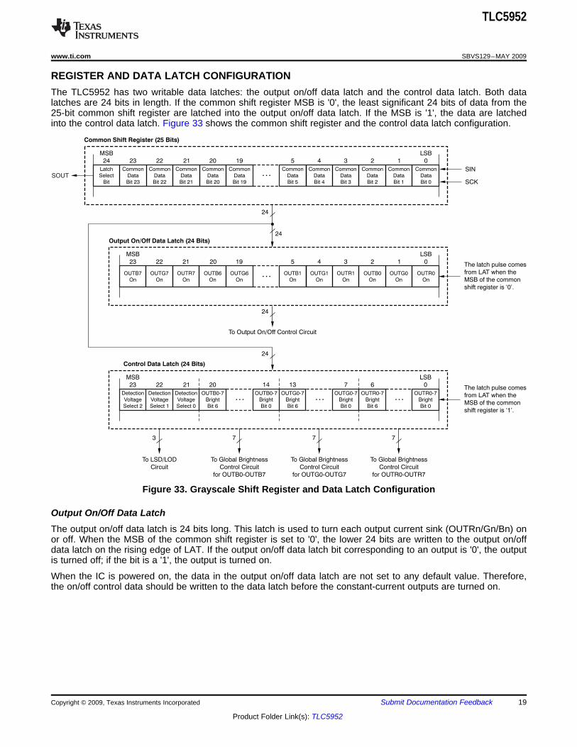
The TLC5952 has two writable data latches: the output on/off data latch and the control data latch. Both datalatches are 24 bits in length. If the common shift register MSB is '0', the least significant 24 bits of data from the25-bit common shift register are latched into the output on/off data latch. If the MSB is '1', the data are latchedinto the control data latch. Figure 33 shows the common shift register and the control data latch configuration.

Figure 33. Grayscale Shift Register and Data Latch Configuration

Output On/Off Data LatchThe output on/off data latch is 24 bits long. This latch is used to turn each output current sink (OUTRn/Gn/Bn) onor off. When the MSB of the common shift register is set to '0', the lower 24 bits are written to the output on/offdata latch on the rising edge of LAT. If the output on/off data latch bit corresponding to an output is '0', the outputis turned off; if the bit is a '1', the output is turned on.

When the IC is powered on, the data in the output on/off data latch are not set to any default value. Therefore,the on/off control data should be written to the data latch before the constant-current outputs are turned on.

Copyright © 2009, Texas Instruments Incorporated Submit Documentation Feedback 19

Product Folder Link(s): TLC5952

TLC5952

SBVS129–MAY 2009........................................................................................................................................................................................................ www.ti.com

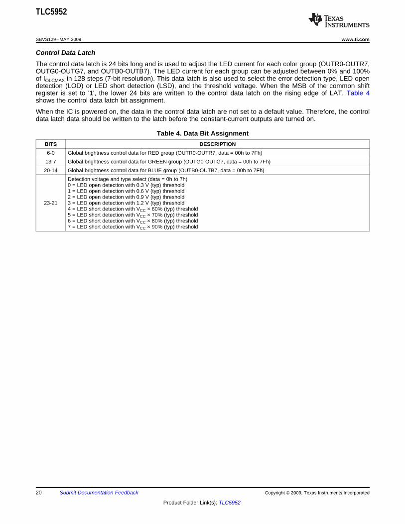
Control Data LatchThe control data latch is 24 bits long and is used to adjust the LED current for each color group (OUTR0-OUTR7,OUTG0-OUTG7, and OUTB0-OUTB7). The LED current for each group can be adjusted between 0% and 100%of IOLCMAX in 128 steps (7-bit resolution). This data latch is also used to select the error detection type, LED opendetection (LOD) or LED short detection (LSD), and the threshold voltage. When the MSB of the common shiftregister is set to '1', the lower 24 bits are written to the control data latch on the rising edge of LAT. Table 4shows the control data latch bit assignment.

When the IC is powered on, the data in the control data latch are not set to a default value. Therefore, the controldata latch data should be written to the latch before the constant-current outputs are turned on.

Table 4. Data Bit AssignmentBITS DESCRIPTION6-0 Global brightness control data for RED group (OUTR0-OUTR7, data = 00h to 7Fh)

13-7 Global brightness control data for GREEN group (OUTG0-OUTG7, data = 00h to 7Fh)20-14 Global brightness control data for BLUE group (OUTB0-OUTB7, data = 00h to 7Fh)

Detection voltage and type select (data = 0h to 7h)0 = LED open detection with 0.3 V (typ) threshold1 = LED open detection with 0.6 V (typ) threshold2 = LED open detection with 0.9 V (typ) threshold

23-21 3 = LED open detection with 1.2 V (typ) threshold4 = LED short detection with VCC × 60% (typ) threshold5 = LED short detection with VCC × 70% (typ) threshold6 = LED short detection with VCC × 80% (typ) threshold7 = LED short detection with VCC × 90% (typ) threshold

20 Submit Documentation Feedback Copyright © 2009, Texas Instruments Incorporated

Product Folder Link(s): TLC5952

¼ ¼ ¼ ¼

¼ ¼ ¼ ¼

Current Data

SOUT

(Common Shift Register Bit 24)

R0B

On

G0B

On

B7B

On

LOD

B7B

LOD

G0B

LOD

R0B

High

23

Cont

0

Cont

LOD

G7B

23

Cont

LOD

R0B

1

Cont

TEF

B

LOD

R0A

23

ContHighB7B

OnLow

0A

On

LowLOD

B7B

TEF

A

SCLK

SIN

OUTR0 ON

OFF

1 2 3 4 5 6

LAT

On/Off Data Latch

(Internal)

BLANK

ON

OFF

ON

OFF

ON

OFF

23 24 25

G7B

On

R7B

On

B6B

On

R0B

On

G0B

On

B0B

On

R6B

On

22

Cont

21

Cont

0

Cont

LOD

G7A

LOD

R7A

LOD

B6A

LOD

G6A

LOD

R6A

LOD

G0A

LOD

G7B

LOD

R7B

LOD

G0B

LOD

R0B

LOD

B7A

1 2 3 23 24 25

Previous Data Current Data

1

Cont

(V )OUTRn/Gn/BnH

(V )OUTRn/Gn/BnL

Control Data Latch

(Internal)Previous Data

OUTG0

OUTB0

OUTR1

OUTR7 ON

OFF

ON

OFF

ON

OFF

OUTG7

OUTB7

Common Shift Register

Bit 0 (Internal)23

ContHighB7B

OnLow

G7B

On

R7B

On

B6B

On

G0B

On

B0B

On

22

Cont

2

Cont

Common Shift Register

Bit 1 (Internal)HighLow

B7B

On

G7B

On

R7B

On

B0B

On

R1B

On

3

Cont

1

Cont

2

Cont

Common Shift Register

Bit 23 (Internal)Low

LOD

R0A

LOD

G7A

LOD

R7A

LOD

B6A

LOD

G6A

LOD

B7A

LOD

R6A

LOD

R0A

LOD

G0A

LOD

R7B

LOD

B6B

LOD

G0B

LOD

R0B

Output On/Off Data Write Control Data Write

G6B

On

G6B

On

B6B

On

LOD

B5A

Output current

is changed

by BC data.

2

Cont

SID data are copied to the 25-bit

common shift register at the

rising edge of LAT.

The LOD/LSD result of each LED comes from SOUT.

The data in the common shift register are copied

to the on/off data latch at the rising edge of LAT.

The data in the common shift register are copied

to the control data latch at the rising edge of LAT.

RED outputs are turned off by the output on/off data.

TLC5952

www.ti.com........................................................................................................................................................................................................ SBVS129–MAY 2009

Figure 34 shows the operation to write data into the common shift register and control data latch.

Figure 34. Data Write Operation

Copyright © 2009, Texas Instruments Incorporated Submit Documentation Feedback 21

Product Folder Link(s): TLC5952

STATUS INFORMATION DATA (SID)

LOD/LSD Holder (24 Bits) and TEF Holder (1 Bit)

LOD or

LSD for

OUTG7

LOD or

LSD for

OUTB7

LOD or

LSD for

OUTG6

Thermal

Error

Flag

¼

LOD or

LSD for

OUTR7

LOD or

LSD for

OUTB6

LOD or

LSD for

OUTR1

LOD or

LSD for

OUTG0

LOD or

LSD for

OUTG1

LOD or

LSD for

OUTB0

LOD or

LSD for

OUTR0

LOD or

LSD for

OUTB1

Common Shift Register (25 Bits)

LSB

Bit 22Bit 23 Bit 19

MSB

Bit 24 ¼Bit 21 Bit 20 Bit 3 Bit 1Bit 4 Bit 2 Bit 0SOUTSCK

SINBit 5

SID are loaded to the

common shift register

at the rising edge of LAT

when the common shift

register MSB is ‘0’.

LED OPEN DETECTION (LOD), LED SHORT DETECTION (LSD), AND THERMAL ERROR FLAG

TLC5952

SBVS129–MAY 2009........................................................................................................................................................................................................ www.ti.com

The 25-bit word status information data (SID) contains the status of the LED open detection (LOD) or LED shortdetection (LSD), and thermal error flag (TEF). When the MSB of the common shift register is set to '0', the SIDoverwrites the common shift register data at the rising edge of LAT after the data in the common shift register arecopied to the output on/off data latch. If the common shift register MSB is '1', the SID data are not copied to thecommon shift register.

After being copied into the common shift register, new SID data are not available until new data are written intothe common shift register. If new data are not written, the LAT signal is ignored. To recheck SID data withoutchanging the constant-current output on/off data, reprogram the common shift register with the same data thatare currently programmed into the output on/off data latch. When LAT goes high, the output on/off data do notchange, but new SID data are loaded into the common shift register. LOD, LSD, and TEF are shifted out ofSOUT with each rising edge of SCLK.

Figure 35. SID Load Assignment

(TEF)LOD detects a fault caused by an LED open circuit or a short from OUTRn/Gn/Bn to ground by comparing theOUTRn/Gn/Bn voltage to the LOD detection threshold voltage level set in the control data latch (Table 4). If theOUTRn/Gn/Bn voltage is lower than the programmed voltage, that output LOD bit is set to '1' to indicate an openLED. Otherwise, the LOD bit is set to '0'. LOD data are only valid for outputs programmed to be on. LOD data foroutputs programmed to be off are always '0'.

LSD data detects a fault caused by a shorted LED by comparing the OUTRn/Gn/Bn voltage to the LSD detectionthreshold voltage level set in the control data latch (Table 4). If the OUTRn/Gn/Bn voltage is higher than theprogrammed voltage, that output LOD bit is set to '1' to indicate a shorted LED. Otherwise, the LSD bit is set to'0'. LSD data are only valid for outputs programmed to be on. LSD data for outputs programmed to be off arealways '0'.

LOD/LSD data are not valid until 1 µs after the falling edge of BLANK. Therefore, BLANK must be low for at least1 µs before going high. At the rising edge of BLANK, the LOD/LSD detection data are latched in the LOD/LSDholder. Changes in the LOD/LSD data while BLANK is low are directly connected to the output of the LOD/LSDholder, but are only valid 1 µs after the change. The rising edge of LAT transfers the output data of the LOD/LSDholder to the common shift register.

22 Submit Documentation Feedback Copyright © 2009, Texas Instruments Incorporated

Product Folder Link(s): TLC5952

THERMAL SHUTDOWN (TSD)

NOISE REDUCTION

CAPACITOR SELECTION

TLC5952

www.ti.com........................................................................................................................................................................................................ SBVS129–MAY 2009

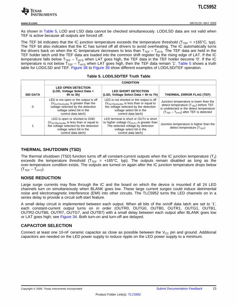
As shown in Table 5, LOD and LSD data cannot be checked simultaneously. LOD/LSD data are not valid whenTEF is active because all outputs are forced off.

The TEF bit indicates that the IC junction temperature exceeds the temperature threshold (TTEF = +165°C, typ).The TEF bit also indicates that the IC has turned off all drivers to avoid overheating. The IC automatically turnsthe drivers back on when the IC temperature decreases to less than TTEF – THYS. The TEF data are held in theTEF holder latch until the TEF data are loaded into the common shift register by the rising edge of LAT. If the ICtemperature falls below TTEF – THYS when LAT goes high, the TEF data in the TEF holder become '0'. If the ICtemperature is not below TTEF – THYS when LAT goes high, then the TEF data remain '1'. Table 5 shows a truthtable for LOD/LSD and TEF. Figure 36 to Figure 39 show different examples of LOD/LSD/TEF operation.

Table 5. LOD/LSD/TEF Truth TableCONDITION

LED OPEN DETECTION(LOD, Voltage Select Data = LED SHORT DETECTION

SID DATA 0h to 3h) (LSD, Voltage Select Data = 4h to 7h) THERMAL ERROR FLAG (TEF)LED is not open or the output is off LED is not shorted or the output is off Junction temperature is lower than the(VOUTRn/Gn/Bn is greater than the (VOUTRn/Gn/Bn is less than or equal to detect temperature (TTEF) before TEF0 voltage selected by the detection the voltage selected by the detection is undetected or the detect temperaturevoltage select bit in the voltage select bit in the (TTEF – THYS) after TEF is detectedcontrol data latch) control data latch)

LED is open or shorted to GND LED terminal is short or OUTn is short(VOUTRn/Gn/Bn is less than or equal to to higher voltage (VOUTn is greater than Junction temperature is higher than the1 the voltage selected by the detection The selected voltage by detection detect temperature (TTEF)voltage select bit in the voltage select bit in the

control data latch) control data latch)

The thermal shutdown (TSD) function turns off all constant-current outputs when the IC junction temperature (TJ)exceeds the temperature threshold (TTEF = +165°C, typ). The outputs remain disabled as long as theover-temperature condition exists. The outputs are turned on again after the IC junction temperature drops below(TTEF – THYS).

Large surge currents may flow through the IC and the board on which the device is mounted if all 24 LEDchannels turn on simultaneously when BLANK goes low. These large current surges could induce detrimentalnoise and electromagnetic interference (EMI) into other circuits. The TLC5952 turns the LED channels on in aseries delay to provide a circuit soft-start feature.

A small delay circuit is implemented between each output. When all bits of the on/off data latch are set to '1',each constant-current output turns on in order (OUTR0, OUTG0, OUTB0, OUTR1, OUTG1, OUTB1,OUTR2-OUTB6, OUTR7, OUTG7, and OUTB7) with a small delay between each output after BLANK goes lowor LAT goes high; see Figure 34. Both turn-on and turn-off are delayed.

Connect at least one 10-nF ceramic capacitor as close as possible between the VCC pin and ground. Additionalcapacitors are needed on the LED power supply to reduce ripple on the LED power supply to a minimum.

Copyright © 2009, Texas Instruments Incorporated Submit Documentation Feedback 23

Product Folder Link(s): TLC5952

22B

On

The data in the common shift register are copied to the control data latch at the rising edge of LAT.

SID data (LOD or LSD and TEF) are loaded into the common shift register at the same time.

TEF

B

LOD

R0A

23C

On

23B

OnLow

0A

On

LowLOD

B7B

TEF

A

SCLK

SIN

OUTXn

OFF

1 2 3 4 5

LAT

BLANK

SOUT

(Common Shift Register)

(Bit 24)

22 23 24 25

21B

On

20B

On

0B

On

1B

On

2B

On

3B

On

22C

On

21C

On

20C

On

17C

On

18C

On

LOD

G7A

LOD

R7A

LOD

B6A

LOD

G6A

LOD

R1A

LOD

B0A

LOD

G0A

LOD

G7B

LOD

R7B

LOD

B6B

LOD

G6B

LOD

R6B

LOD

G5B

LOD

B7A

1 2 3 4 5 6 7

19C

On

16C

On

LOD

B5B

(LOD Voltage)

SID data are copied to the 25-bit common shift register at the

rising edge of LAT with the common shift register MSB low.

0 V

LOD/LSD Data

For OUTXn

(Internal)

'0' '0'

(LSD Voltage)

Low

ON ON

22B

On

The data in the common shift register are copied to the control data latch at the rising edge of LAT.

SID data (LOD or LSD and TEF) are loaded into the common shift register at the same time.

TEF

B

LOD

R0A

23C

On

23B

OnLow

0A

On

LowLOD

B7B

TEF

A

SCLK

SIN

1 2 3 4 5

LAT

BLANK

SOUT

(Common Shift Register)

(Bit 24)

22 23 24 25

21B

On

20B

On

0B

On

1B

On

2B

On

3B

On

22C

On

21C

On

20C

On

17C

On

18C

On

LOD

G7A

LOD

R7A

LOD

B6A

LOD

G6A

LOD

R1A

LOD

B0A

LOD

G0A

LOD

G7B

LOD

R7B

LOD

B6B

LOD

G6B

LOD

R6B

LOD

G5B

LOD

B7A

1 2 3 4 5 6 7

19C

On

16C

On

LOD

B5B

Low

OUTXnON

OFF

(LOD Voltage)

(LSD Voltage)

ON0 V

LOD Circuit Output

For OUTXn

(Internal)'0' (LED is Not Open)

'1' (LED is Open)

'1' (LED is Open)

LED is Open At This Time

'1' (LED is Open)

'1' (LED is Open)

LOD output becomes '0' when the output is off.

LOD Data In LOD/LSD Holder

(Internal)LOD data are not updated while BLANK is high.

Therefore, LOD data in previous display periods

can be read even if BLANK is high.LOD data are immediately updated with the

LOD circuit output when BLANK is low.

SID data are copied to the 25-bit common shift register at the

rising edge of LAT with the common shift register MSB low.

TLC5952

SBVS129–MAY 2009........................................................................................................................................................................................................ www.ti.com

Figure 36. LOD/LSD/TEF Operation (No LED Error)

Figure 37. LOD/LSD/TEF Operation (LED Open Error)

24 Submit Documentation Feedback Copyright © 2009, Texas Instruments Incorporated

Product Folder Link(s): TLC5952

22B

On

The data in the common shift register are copied to the control data latch at the rising edge of LAT.

SID data (LOD or LSD and TEF) are loaded into the common shift register at the same time.

TEF

B

LOD

R0A

23C

On

23B

OnLow

0A

On

LowLOD

B7B

TEF

A

SCLK

SIN

1 2 3 4 5

LAT

BLANK

SOUT

(Common Shift Register)

(Bit 24)

22 23 24 25

21B

On

20B

On

0B

On

1B

On

2B

On

3B

On

22C

On

21C

On

20C

On

17C

On

18C

On

LOD

G7A

LOD

R7A

LOD

B6A

LOD

G6A

LOD

R1A

LOD

B0A

LOD

G0A

LOD

G7B

LOD

R7B

LOD

B6B

LOD

G6B

LOD

R6B

LOD

G5B

LOD

B7A

1 2 3 4 5 6 7

19C

On

16C

On

LOD

B5B

Low

SID data are copied to the 25-bit common shift register at the

rising edge of LAT with the common shift register MSB low.

OUTXnON

OFF

(LSD Voltage)

ON

0 V

LSD Circuit Output

For OUTXn

(Internal)

'1' (LED is Shorted)

'0' (LED is Not Shorted)

'1' (LED is Shorted)

LED is Shorted At This Time

'1' (LED is Shorted)

'1' (LED is Shorted)

LSD output becomes '0' when the output is off.

LSD Data In LOD/LSD Holder

(Internal)

LSD data are immediately updated with the

LSD circuit output when BLANK is low.

LSD data are not updated while BLANK is high.

Therefore, LSD data in previous display periods

can be read even if BLANK is high.

22B

On

The data in the common shift register are copied to the control data latch at the rising edge of LAT.

SID data (LOD or LSD and TEF) are loaded into the common shift register at the same time.

TEF

B

LOD

R0A

23C

On

23B

OnLow

0A

On

LowLOD

B7B

TEF

A

SCLK

SIN

1 2 3 4 5

LAT

BLANK

SOUT

(Common Shift Register)

(Bit 24)

22 23 24 25

21B

On

20B

On

0B

On

1B

On

2B

On

3B

On

22C

On

21C

On

20C

On

17C

On

18C

On

LOD

G7A

LOD

R7A

LOD

B6A

LOD

G6A

LOD

R1A

LOD

B0A

LOD

G0A

LOD

G7B

LOD

R7B

LOD

B6B

LOD

G6B

LOD

R6B

LOD

G5B

LOD

B7A

1 2 3 4 5 6 7

19C

On

16C

On

LOD

B5B

Low

SID data are copied to the 25-bit common shift register at the

rising edge of LAT with the common shift register MSB low.

Thermal Detector Output

(Internal) '0' (Temperature is Normal)

'0' (Temperature is Normal)

'1' (Temperature is Higher Than T )TEF'1' (Temperature is Higher Than T )TEF

'1' (Temperature is Higher Than T )TEF '1' (Temperature is Higher Than T )TEF

The output becomes '0' because the

temperature drops below T T

when the output is off.

-TEF HYS

TEF Data In TEF Holder

(Internal)

TEF data are immediately

updated when BLANK is low.

TEF data are set to '1' when the junction temperature exceeds T . The TEF data are held in

the TEF holder until the SID data are loaded into the common shift register. The TEF data are reset to '0'

at the rising edge of LAT if the junction temperature is below T T .-

TEF

TEF HYS

TLC5952

www.ti.com........................................................................................................................................................................................................ SBVS129–MAY 2009

Figure 38. LOD/LSD/TEF Operation (LED Short Error)

Figure 39. LOD/LSD/TEF Operation (Thermal Error)

Copyright © 2009, Texas Instruments Incorporated Submit Documentation Feedback 25

Product Folder Link(s): TLC5952

PACKAGE OPTION ADDENDUM

www.ti.com 11-Apr-2013

Addendum-Page 1

PACKAGING INFORMATION

Orderable Device Status(1)

Package Type PackageDrawing

Pins PackageQty

Eco Plan(2)

Lead/Ball Finish MSL Peak Temp(3)

Op Temp (°C) Top-Side Markings(4)

Samples

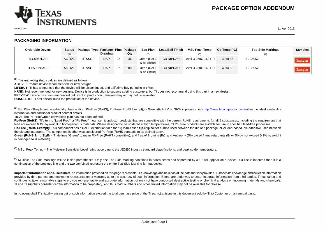
TLC5952DAP ACTIVE HTSSOP DAP 32 46 Green (RoHS& no Sb/Br)

CU NIPDAU Level-3-260C-168 HR -40 to 85 TLC5952

TLC5952DAPR ACTIVE HTSSOP DAP 32 2000 Green (RoHS& no Sb/Br)

CU NIPDAU Level-3-260C-168 HR -40 to 85 TLC5952

(1) The marketing status values are defined as follows:ACTIVE: Product device recommended for new designs.LIFEBUY: TI has announced that the device will be discontinued, and a lifetime-buy period is in effect.NRND: Not recommended for new designs. Device is in production to support existing customers, but TI does not recommend using this part in a new design.PREVIEW: Device has been announced but is not in production. Samples may or may not be available.OBSOLETE: TI has discontinued the production of the device.

(2) Eco Plan - The planned eco-friendly classification: Pb-Free (RoHS), Pb-Free (RoHS Exempt), or Green (RoHS & no Sb/Br) - please check http://www.ti.com/productcontent for the latest availabilityinformation and additional product content details.TBD: The Pb-Free/Green conversion plan has not been defined.Pb-Free (RoHS): TI's terms "Lead-Free" or "Pb-Free" mean semiconductor products that are compatible with the current RoHS requirements for all 6 substances, including the requirement thatlead not exceed 0.1% by weight in homogeneous materials. Where designed to be soldered at high temperatures, TI Pb-Free products are suitable for use in specified lead-free processes.Pb-Free (RoHS Exempt): This component has a RoHS exemption for either 1) lead-based flip-chip solder bumps used between the die and package, or 2) lead-based die adhesive used betweenthe die and leadframe. The component is otherwise considered Pb-Free (RoHS compatible) as defined above.Green (RoHS & no Sb/Br): TI defines "Green" to mean Pb-Free (RoHS compatible), and free of Bromine (Br) and Antimony (Sb) based flame retardants (Br or Sb do not exceed 0.1% by weightin homogeneous material)

(3) MSL, Peak Temp. -- The Moisture Sensitivity Level rating according to the JEDEC industry standard classifications, and peak solder temperature.

(4) Multiple Top-Side Markings will be inside parentheses. Only one Top-Side Marking contained in parentheses and separated by a "~" will appear on a device. If a line is indented then it is acontinuation of the previous line and the two combined represent the entire Top-Side Marking for that device.

Important Information and Disclaimer:The information provided on this page represents TI's knowledge and belief as of the date that it is provided. TI bases its knowledge and belief on informationprovided by third parties, and makes no representation or warranty as to the accuracy of such information. Efforts are underway to better integrate information from third parties. TI has taken andcontinues to take reasonable steps to provide representative and accurate information but may not have conducted destructive testing or chemical analysis on incoming materials and chemicals.TI and TI suppliers consider certain information to be proprietary, and thus CAS numbers and other limited information may not be available for release.

In no event shall TI's liability arising out of such information exceed the total purchase price of the TI part(s) at issue in this document sold by TI to Customer on an annual basis.

TAPE AND REEL INFORMATION

*All dimensions are nominal

Device PackageType

PackageDrawing

Pins SPQ ReelDiameter

(mm)

ReelWidth

W1 (mm)

A0(mm)

B0(mm)

K0(mm)

P1(mm)

W(mm)

Pin1Quadrant

TLC5952DAPR HTSSOP DAP 32 2000 330.0 24.4 8.6 11.5 1.6 12.0 24.0 Q1

PACKAGE MATERIALS INFORMATION

www.ti.com 20-Jul-2016

Pack Materials-Page 1

*All dimensions are nominal

Device Package Type Package Drawing Pins SPQ Length (mm) Width (mm) Height (mm)

TLC5952DAPR HTSSOP DAP 32 2000 367.0 367.0 45.0

PACKAGE MATERIALS INFORMATION

www.ti.com 20-Jul-2016

Pack Materials-Page 2

IMPORTANT NOTICE

Texas Instruments Incorporated and its subsidiaries (TI) reserve the right to make corrections, enhancements, improvements and otherchanges to its semiconductor products and services per JESD46, latest issue, and to discontinue any product or service per JESD48, latestissue. Buyers should obtain the latest relevant information before placing orders and should verify that such information is current andcomplete. All semiconductor products (also referred to herein as “components”) are sold subject to TI’s terms and conditions of salesupplied at the time of order acknowledgment.TI warrants performance of its components to the specifications applicable at the time of sale, in accordance with the warranty in TI’s termsand conditions of sale of semiconductor products. Testing and other quality control techniques are used to the extent TI deems necessaryto support this warranty. Except where mandated by applicable law, testing of all parameters of each component is not necessarilyperformed.TI assumes no liability for applications assistance or the design of Buyers’ products. Buyers are responsible for their products andapplications using TI components. To minimize the risks associated with Buyers’ products and applications, Buyers should provideadequate design and operating safeguards.TI does not warrant or represent that any license, either express or implied, is granted under any patent right, copyright, mask work right, orother intellectual property right relating to any combination, machine, or process in which TI components or services are used. Informationpublished by TI regarding third-party products or services does not constitute a license to use such products or services or a warranty orendorsement thereof. Use of such information may require a license from a third party under the patents or other intellectual property of thethird party, or a license from TI under the patents or other intellectual property of TI.Reproduction of significant portions of TI information in TI data books or data sheets is permissible only if reproduction is without alterationand is accompanied by all associated warranties, conditions, limitations, and notices. TI is not responsible or liable for such altereddocumentation. Information of third parties may be subject to additional restrictions.Resale of TI components or services with statements different from or beyond the parameters stated by TI for that component or servicevoids all express and any implied warranties for the associated TI component or service and is an unfair and deceptive business practice.TI is not responsible or liable for any such statements.Buyer acknowledges and agrees that it is solely responsible for compliance with all legal, regulatory and safety-related requirementsconcerning its products, and any use of TI components in its applications, notwithstanding any applications-related information or supportthat may be provided by TI. Buyer represents and agrees that it has all the necessary expertise to create and implement safeguards whichanticipate dangerous consequences of failures, monitor failures and their consequences, lessen the likelihood of failures that might causeharm and take appropriate remedial actions. Buyer will fully indemnify TI and its representatives against any damages arising out of the useof any TI components in safety-critical applications.In some cases, TI components may be promoted specifically to facilitate safety-related applications. With such components, TI’s goal is tohelp enable customers to design and create their own end-product solutions that meet applicable functional safety standards andrequirements. Nonetheless, such components are subject to these terms.No TI components are authorized for use in FDA Class III (or similar life-critical medical equipment) unless authorized officers of the partieshave executed a special agreement specifically governing such use.Only those TI components which TI has specifically designated as military grade or “enhanced plastic” are designed and intended for use inmilitary/aerospace applications or environments. Buyer acknowledges and agrees that any military or aerospace use of TI componentswhich have not been so designated is solely at the Buyer's risk, and that Buyer is solely responsible for compliance with all legal andregulatory requirements in connection with such use.TI has specifically designated certain components as meeting ISO/TS16949 requirements, mainly for automotive use. In any case of use ofnon-designated products, TI will not be responsible for any failure to meet ISO/TS16949.

Products ApplicationsAudio www.ti.com/audio Automotive and Transportation www.ti.com/automotiveAmplifiers amplifier.ti.com Communications and Telecom www.ti.com/communicationsData Converters dataconverter.ti.com Computers and Peripherals www.ti.com/computersDLP® Products www.dlp.com Consumer Electronics www.ti.com/consumer-appsDSP dsp.ti.com Energy and Lighting www.ti.com/energyClocks and Timers www.ti.com/clocks Industrial www.ti.com/industrialInterface interface.ti.com Medical www.ti.com/medicalLogic logic.ti.com Security www.ti.com/securityPower Mgmt power.ti.com Space, Avionics and Defense www.ti.com/space-avionics-defenseMicrocontrollers microcontroller.ti.com Video and Imaging www.ti.com/videoRFID www.ti-rfid.comOMAP Applications Processors www.ti.com/omap TI E2E Community e2e.ti.comWireless Connectivity www.ti.com/wirelessconnectivity

Mailing Address: Texas Instruments, Post Office Box 655303, Dallas, Texas 75265Copyright © 2016, Texas Instruments Incorporated


Recommended