256/512/1K/2K/4K x 9 Asynchronous FIFO CY7C419/21/25/29/33 Cypress Semiconductor Corporation • 3901 North First Street • San Jose, CA 95134 • 408-943-2600 Document #: 38-06001 Rev. *B Revised June 30, 2005 Features • Asynchronous first-in first-out (FIFO) buffer memories • 256 x 9 (CY7C419) • 512 x 9 (CY7C421) • 1K x 9 (CY7C425) • 2K x 9 (CY7C429) • 4K x 9 (CY7C433) • Dual-ported RAM cell • High-speed 50.0-MHz read/write independent of depth/width • Low operating power: I CC = 35 mA • Empty and Full flags (Half Full flag in standalone) • TTL compatible • Retransmit in standalone • Expandable in width • PLCC, 7x7 TQFP, SOJ, 300-mil and 600-mil DIP • Pb-Free Packages Available • Pin compatible and functionally equivalent to IDT7200, IDT7201, IDT7202, IDT7203, IDT7204, AM7200, AM7201, AM7202, AM7203, and AM7204 Functional Description The CY7C419, CY7C420/1, CY7C424/5, CY7C428/9, and CY7C432/3 are first-in first-out (FIFO) memories offered in 600-mil wide and 300-mil wide packages. They are, respec- tively, 256, 512, 1,024, 2,048, and 4,096 words by 9-bits wide. Each FIFO memory is organized such that the data is read in the same sequential order that it was written. Full and Empty flags are provided to prevent overrun and underrun. Three additional pins are also provided to facilitate unlimited expansion in width, depth, or both. The depth expansion technique steers the control signals from one device to another in parallel, thus eliminating the serial addition of propagation delays, so that throughput is not reduced. Data is steered in a similar manner. The read and write operations may be asynchronous; each can occur at a rate of 50.0 MHz. The write operation occurs when the write (W ) signal is LOW. Read occurs when read (R ) goes LOW. The nine data outputs go to the high-impedance state when R is HIGH. A Half Full (HF ) output flag is provided that is valid in the standalone and width expansion configurations. In the depth expansion configuration, this pin provides the expansion out (XO ) information that is used to tell the next FIFO that it will be activated. In the standalone and width expansion configurations, a LOW on the retransmit (RT ) input causes the FIFOs to retransmit the data. Read enable (R ) and write enable (W ) must both be HIGH during retransmit, and then R is used to access the data. The CY7C419, CY7C420, CY7C421, CY7C424, CY7C425, CY7C428, CY7C429, CY7C432, and CY7C433 are fabricated using an advanced 0.65-micron P-well CMOS technology. Input ESD protection is greater than 2000V and latch-up is prevented by careful layout and guard rings. CY7C419/21/25/29/33256/512/1K/2K/4K x 9 Asynchronous FIFO
Transcript
256/512/1K/2K/4K x 9 Asynchronous FIFO
CY7C419/21/25/29/33
Cypress Semiconductor Corporation • 3901 North First Street • San Jose, CA 95134 • 408-943-2600Document #: 38-06001 Rev. *B Revised June 30, 2005
Features• Asynchronous first-in first-out (FIFO) buffer memories• 256 x 9 (CY7C419)• 512 x 9 (CY7C421)• 1K x 9 (CY7C425)• 2K x 9 (CY7C429)• 4K x 9 (CY7C433)• Dual-ported RAM cell• High-speed 50.0-MHz read/write independent of
depth/width• Low operating power: ICC = 35 mA• Empty and Full flags (Half Full flag in standalone)• TTL compatible• Retransmit in standalone• Expandable in width• PLCC, 7x7 TQFP, SOJ, 300-mil and 600-mil DIP • Pb-Free Packages Available• Pin compatible and functionally equivalent to IDT7200,
IDT7201, IDT7202, IDT7203, IDT7204, AM7200, AM7201, AM7202, AM7203, and AM7204
Functional DescriptionThe CY7C419, CY7C420/1, CY7C424/5, CY7C428/9, andCY7C432/3 are first-in first-out (FIFO) memories offered in
600-mil wide and 300-mil wide packages. They are, respec-tively, 256, 512, 1,024, 2,048, and 4,096 words by 9-bits wide.Each FIFO memory is organized such that the data is read inthe same sequential order that it was written. Full and Emptyflags are provided to prevent overrun and underrun. Threeadditional pins are also provided to facilitate unlimitedexpansion in width, depth, or both. The depth expansiontechnique steers the control signals from one device toanother in parallel, thus eliminating the serial addition ofpropagation delays, so that throughput is not reduced. Data issteered in a similar manner.The read and write operations may be asynchronous; eachcan occur at a rate of 50.0 MHz. The write operation occurswhen the write (W) signal is LOW. Read occurs when read (R)goes LOW. The nine data outputs go to the high-impedancestate when R is HIGH.A Half Full (HF) output flag is provided that is valid in thestandalone and width expansion configurations. In the depthexpansion configuration, this pin provides the expansion out(XO) information that is used to tell the next FIFO that it will beactivated.In the standalone and width expansion configurations, a LOWon the retransmit (RT) input causes the FIFOs to retransmitthe data. Read enable (R) and write enable (W) must both beHIGH during retransmit, and then R is used to access the data.The CY7C419, CY7C420, CY7C421, CY7C424, CY7C425,CY7C428, CY7C429, CY7C432, and CY7C433 are fabricatedusing an advanced 0.65-micron P-well CMOS technology.Input ESD protection is greater than 2000V and latch-up isprevented by careful layout and guard rings.
CY7C419/21/25/29/33256/512/1K/2K/4K x 9 Asynchronous FIFO
CY7C419/21/25/29/33
Document #: 38-06001 Rev. *B Page 2 of 25
Maximum Rating[1]
(Above which the useful life may be impaired. For user guide-lines, not tested.)Storage Temperature .................................–65°C to +150°CAmbient Temperature withPower Applied.............................................–55°C to +125°CSupply Voltage to Ground Potential ............... –0.5V to +7.0V
DC Voltage Applied to Outputsin High Z State ................................................–0.5V to +7.0VDC Input Voltage ............................................–0.5V to +7.0VPower Dissipation.......................................................... 1.0WOutput Current, into Outputs (LOW)............................ 20 mAStatic Discharge Voltage............................................ >2000V(per MIL–STD–883, Method 3015)Latch-Up Current ..................................................... >200 mA
Note: 1. Single Power Supply: The voltage on any input or I/O pin can not exceed the power pin during power-up.
RAM ARRAY256x 9512x 91024x 92048x 94096x 9
Logic Block Diagram Pin Configurations
123456789101112
151617181920
24232221
1314
25
282726
Top ViewDIP
7C420/1
WD8D3D2D1D0XI
FFQ0Q1Q2
GND
VccD4
FL/RTMREFXO/HFQ7
R
PLCC/LCCTop View
Q3Q8
D5D6D7
Q6Q5Q4
4 3 2 1 323130
14 15 1617 181920
5678910111213
292827262524232221
FL/RTMREFXO/HFQ7
D6
Q6
D7NC
READCONTROL
WRITECONTROL
WRITEPOINTER
RESETLOGIC
EXPANSIONLOGIC
DATA INPUTS(D0–D 8)
THREE-STATE
BUFFERS
DATA OUTPUTS(Q0–Q8)
W
READPOINTER
FLAGLOGIC
R
XI
EFFF
XO/HF
MRFL/RT
D2D1D0XI
FFQ0Q1NCQ2
D D W NC
V D D3 8 cc 4 5
Q
Q
GN
DN
C R Q
Q 3 8 4 5
7C4197C421/5/9
7C433 7C424/57C428/97C432/3
7C419
2612345678
2423222120191817
9 10 11 12 13 14 15
32 3130 29 28 27 25
Q1
XI
Q0
D1D0NCNC
FF
D6
D5
D4
V CC
WD8
D3
D2
D7FL/RTNCNCMREFXO/HFQ7
Top ViewTQFP
Q2
Q3
Q8
GN
D R Q4
Q5
Q6
16
7C4197C421/5/9
7C433
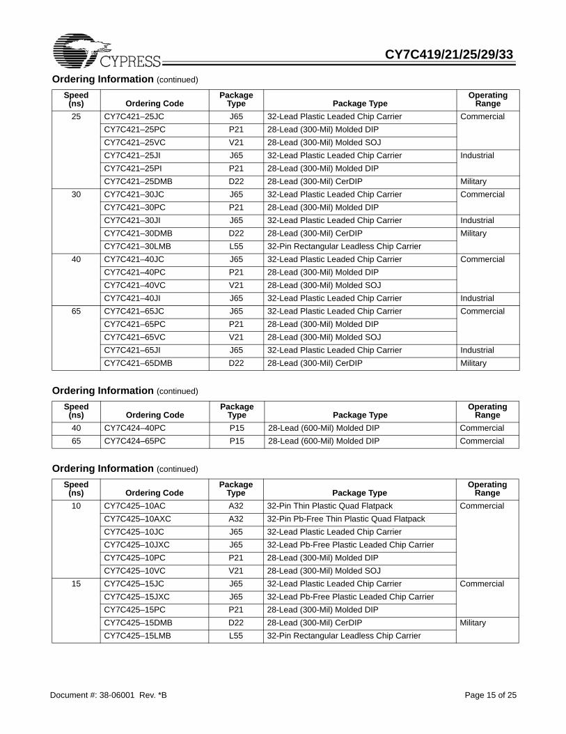
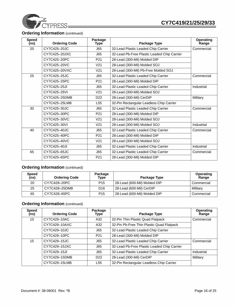
Selection Guide256 x 9 7C419–10 7C419–15 7C419–30 7C419–40512 x 9 (600-mil only) 7C420–20 7C420–25 7C420–40 7C420–65512 x 9 7C421–10 7C421–15 7C421–20 7C421–25 7C421–30 7C421–40 7C421–651K x 9 (600-mil only) 7C424–20 7C424–25 7C424–30 7C424–40 7C424–651K x 9 7C425–10 7C425–15 7C425–20 7C425–25 7C425–30 7C425–40 7C425–652K x 9 (600-mil only) 7C428–20 7C428–652K x 9 7C429–10 7C429–15 7C429–20 7C429–25 7C429–30 7C429–40 7C429–654K x 9 (600-mil only) 7C432–25 7C432–404K x 9 7C433–10 7C433–15 7C433–20 7C433–25 7C433–30 7C433–40 7C433–65Frequency (MHz) 50 40 33.3 28.5 25 20 12.5Maximum Access Time (ns) 10 15 20 25 30 40 65ICC1 (mA) 35 35 35 35 35 35 35
CY7C419/21/25/29/33
Document #: 38-06001 Rev. *B Page 3 of 25
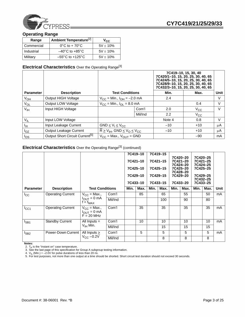
Operating RangeRange Ambient Temperature[2] VCC
Commercial 0°C to + 70°C 5V ± 10%Industrial –40°C to +85°C 5V ± 10%Military –55°C to +125°C 5V ± 10%
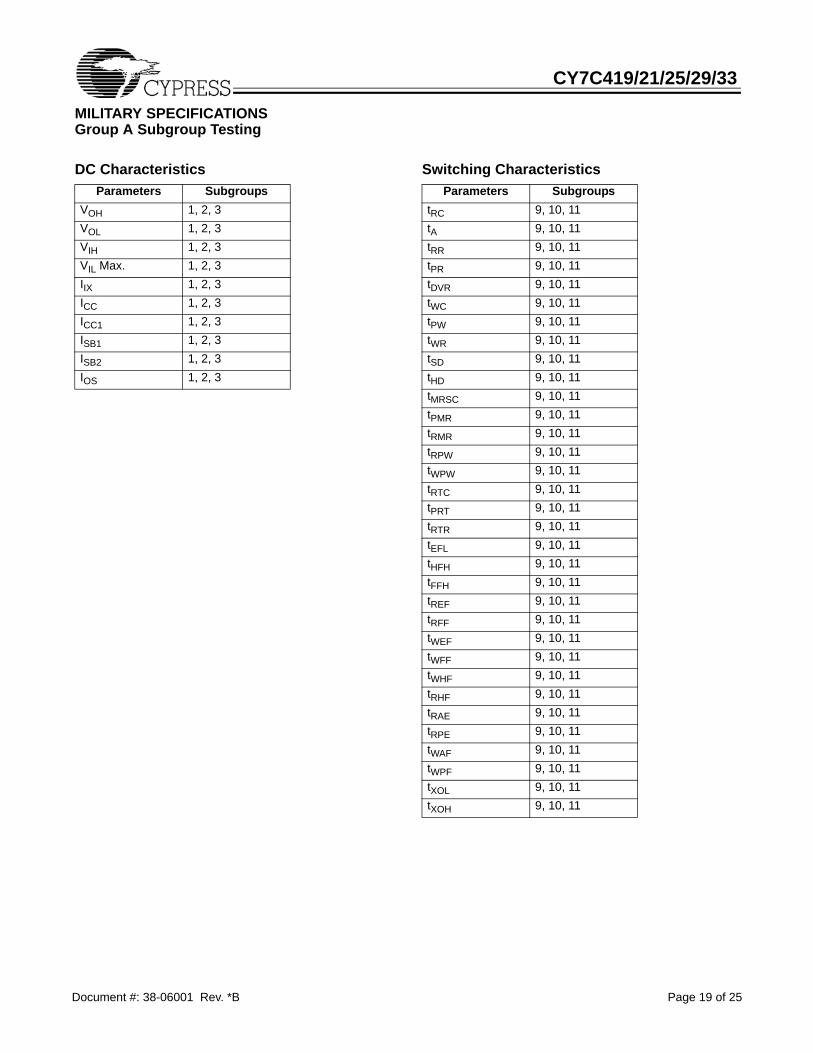
Electrical Characteristics Over the Operating Range[3]
Parameter Description Test Conditions Min. Max. UnitVOH Output HIGH Voltage VCC = Min., IOH = –2.0 mA 2.4 VVOL Output LOW Voltage VCC = Min., IOL = 8.0 mA 0.4 VVIH Input HIGH Voltage Com’l 2.0 VCC V
Mil/Ind 2.2 VCCVIL Input LOW Voltage Note 4 0.8 VIIX Input Leakage Current GND < VI < VCC –10 +10 µAIOZ Output Leakage Current R > VIH, GND < VO < VCC –10 +10 µAIOS Output Short Circuit Current[5] VCC = Max., VOUT = GND –90 mA
Electrical Characteristics Over the Operating Range[3] (continued)
7C419–10
7C421–10
7C425–10
7C429–10
7C433–10
7C419–15
7C421–15
7C425–15
7C429–15
7C433–15
7C420–207C421–207C424–207C425–207C428–207C429–20
7C433–20
7C420–257C421–257C424–257C425–25
7C429–257C432–257C433–25
Parameter Description Test Conditions Min. Max. Min. Max. Min. Max. Min. Max. UnitICC Operating Current VCC = Max.,
Notes: 2. TA is the “instant on” case temperature.3. See the last page of this specification for Group A subgroup testing information.4. VIL (Min.) = –2.0V for pulse durations of less than 20 ns.5. For test purposes, not more than one output at a time should be shorted. Short circuit test duration should not exceed 30 seconds.
CY7C419/21/25/29/33
Document #: 38-06001 Rev. *B Page 4 of 25
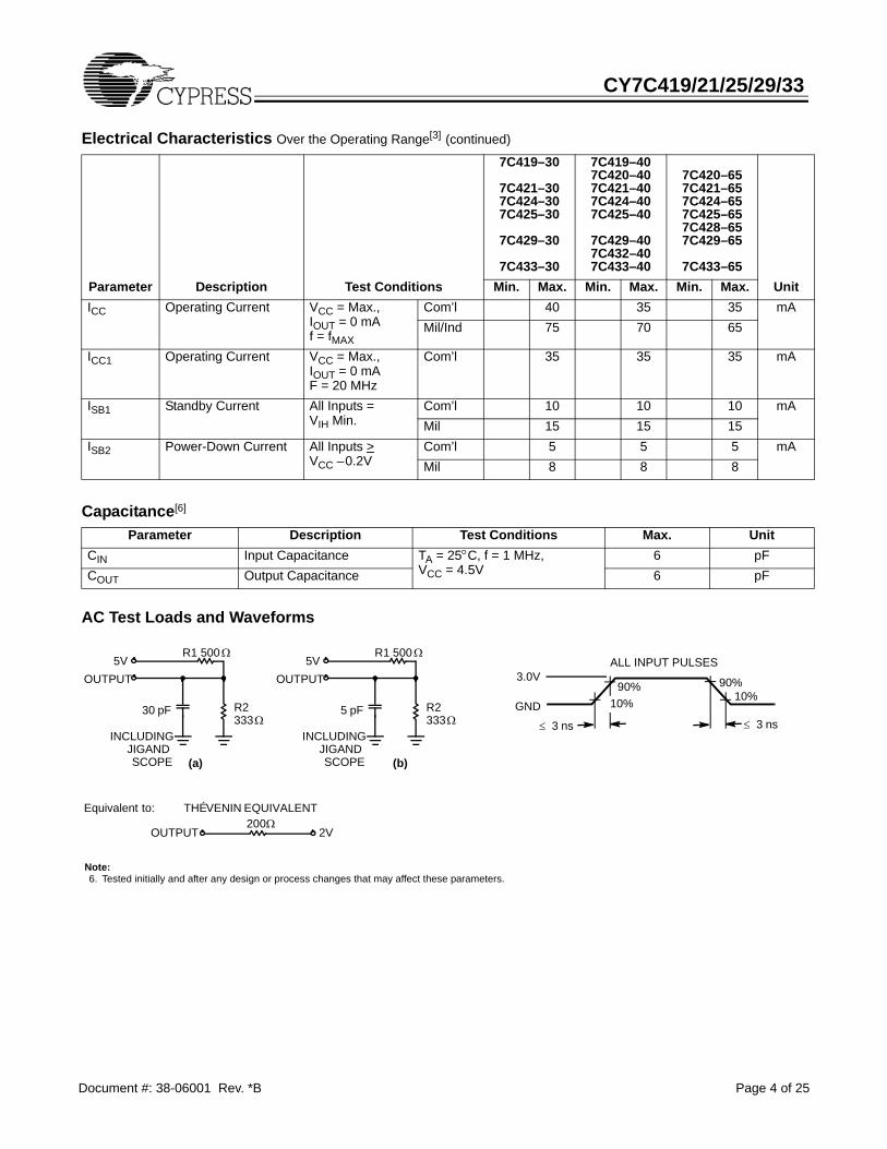
Electrical Characteristics Over the Operating Range[3] (continued)
7C419–30
7C421–307C424–307C425–30
7C429–30
7C433–30
7C419–407C420–407C421–407C424–407C425–40
7C429–407C432–407C433–40
7C420–657C421–657C424–657C425–657C428–657C429–65
7C433–65Parameter Description Test Conditions Min. Max. Min. Max. Min. Max. UnitICC Operating Current VCC = Max.,
Parameter Description Test Conditions Max. UnitCIN Input Capacitance TA = 25°C, f = 1 MHz,
VCC = 4.5V6 pF
COUT Output Capacitance 6 pF
AC Test Loads and Waveforms
Note: 6. Tested initially and after any design or process changes that may affect these parameters.
3.0V5V
OUTPUT
R1 500Ω
R2333Ω
30 pF
INCLUDINGJIGANDSCOPE
GND
90%10%
90%10%
≤ 3 ns ≤ 3 ns
5VOUTPUT
R1 500Ω
R2333Ω
5 pF
INCLUDINGJIGANDSCOPE
OUTPUT 2V
Equivalent to: THÉ VENIN EQUIVALENT
(b)(a)
ALL INPUT PULSES
200Ω
CY7C419/21/25/29/33
Document #: 38-06001 Rev. *B Page 5 of 25
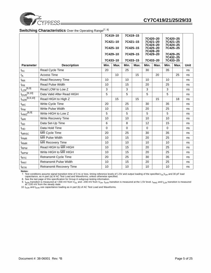
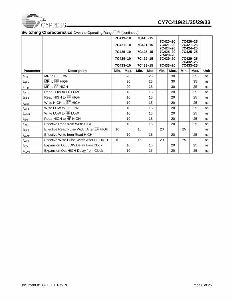
Switching Characteristics Over the Operating Range[7, 8] 7C419–10
7C421–10
7C425–10
7C429–10
7C433–10
7C419–15
7C421–15
7C425–15
7C429–15
7C433–15
7C420–207C421–207C424–207C425–207C428–207C429–20
7C433–20
7C420–257C421–257C424–257C425–25
7C429–257C432–257C433–25
Parameter Description Min. Max. Min. Max. Min. Max. Min. Max. UnittRC Read Cycle Time 20 25 30 35 nstA Access Time 10 15 20 25 nstRR Read Recovery Time 10 10 10 10 nstPR Read Pulse Width 10 15 20 25 nstLZR
[6,9] Read LOW to Low Z 3 3 3 3 nstDVR
[9,10] Data Valid After Read HIGH 5 5 5 5 nstHZR
[6,9,10] Read HIGH to High Z 15 15 15 18 nstWC Write Cycle Time 20 25 30 35 nstPW Write Pulse Width 10 15 20 25 nstHWZ
[6,9] Write HIGH to Low Z 5 5 5 5 nstWR Write Recovery Time 10 10 10 10 nstSD Data Set-Up Time 6 8 12 15 nstHD Data Hold Time 0 0 0 0 nstMRSC MR Cycle Time 20 25 30 35 nstPMR MR Pulse Width 10 15 20 25 nstRMR MR Recovery Time 10 10 10 10 nstRPW Read HIGH to MR HIGH 10 15 20 25 nstWPW Write HIGH to MR HIGH 10 15 20 25 nstRTC Retransmit Cycle Time 20 25 30 35 nstPRT Retransmit Pulse Width 10 15 20 25 nstRTR Retransmit Recovery Time 10 10 10 10 nsNotes: 7. Test conditions assume signal transition time of 3 ns or less, timing reference levels of 1.5V and output loading of the specified IOL/IOH and 30 pF load
capacitance, as in part (a) of AC Test Load and Waveforms, unless otherwise specified.8. See the last page of this specification for Group A subgroup testing information.9. tHZR transition is measured at +200 mV from VOL and –200 mV from VOH. tDVR transition is measured at the 1.5V level. tHWZ and tLZR transition is measured
at ±100 mV from the steady state.10. tHZR and tDVR use capacitance loading as in part (b) of AC Test Load and Waveforms.
CY7C419/21/25/29/33
Document #: 38-06001 Rev. *B Page 6 of 25
tEFL MR to EF LOW 20 25 30 35 nstHFH MR to HF HIGH 20 25 30 35 nstFFH MR to FF HIGH 20 25 30 35 nstREF Read LOW to EF LOW 10 15 20 25 nstRFF Read HIGH to FF HIGH 10 15 20 25 nstWEF Write HIGH to EF HIGH 10 15 20 25 nstWFF Write LOW to FF LOW 10 15 20 25 nstWHF Write LOW to HF LOW 10 15 20 25 nstRHF Read HIGH to HF HIGH 10 15 20 25 nstRAE Effective Read from Write HIGH 10 15 20 25 nstRPE Effective Read Pulse Width After EF HIGH 10 15 20 25 nstWAF Effective Write from Read HIGH 10 15 20 25 nstWPF Effective Write Pulse Width After FF HIGH 10 15 20 25 nstXOL Expansion Out LOW Delay from Clock 10 15 20 25 nstXOH Expansion Out HIGH Delay from Clock 10 15 20 25 ns
Switching Characteristics Over the Operating Range[7, 8] (continued)7C419–10
7C421–10
7C425–10
7C429–10
7C433–10
7C419–15
7C421–15
7C425–15
7C429–15
7C433–15
7C420–207C421–207C424–207C425–207C428–207C429–20
7C433–20
7C420–257C421–257C424–257C425–25
7C429–257C432–257C433–25
Parameter Description Min. Max. Min. Max. Min. Max. Min. Max. Unit
CY7C419/21/25/29/33
Document #: 38-06001 Rev. *B Page 7 of 25
Switching Characteristics Over the Operating Range[7, 8] (continued)
7C419–30
7C421–307C424–307C425–30
7C429–30
7C433–30
7C419–407C420–407C421–407C424–407C425–40
7C429–407C432–407C433–40
7C420–657C421–657C424–657C425–657C428–657C429–65
7C433–65Parameter Description Min. Max. Min. Max. Min. Max. Unit
tRC Read Cycle Time 40 50 80 nstA Access Time 30 40 65 nstRR Read Recovery Time 10 10 15 nstPR Read Pulse Width 30 40 65 nstLZR
[6,9] Read LOW to Low Z 3 3 3 nstDVR
[9,10] Data Valid After Read HIGH 5 5 5 nstHZR
[6,9,10] Read HIGH to High Z 20 20 20 nstWC Write Cycle Time 40 50 80 nstPW Write Pulse Width 30 40 65 nstHWZ
[6,9] Write HIGH to Low Z 5 5 5 nstWR Write Recovery Time 10 10 15 nstSD Data Set-Up Time 18 20 30 nstHD Data Hold Time 0 0 0 nstMRSC MR Cycle Time 40 50 80 nstPMR MR Pulse Width 30 40 65 nstRMR MR Recovery Time 10 10 15 nstRPW Read HIGH to MR HIGH 30 40 65 nstWPW Write HIGH to MR HIGH 30 40 65 nstRTC Retransmit Cycle Time 40 50 80 nstPRT Retransmit Pulse Width 30 40 65 nstRTR Retransmit Recovery Time 10 10 15 nstEFL MR to EF LOW 40 50 80 nstHFH MR to HF HIGH 40 50 80 nstFFH MR to FF HIGH 40 50 80 nstREF Read LOW to EF LOW 30 35 60 nstRFF Read HIGH to FF HIGH 30 35 60 nstWEF Write HIGH to EF HIGH 30 35 60 nstWFF Write LOW to FF LOW 30 35 60 nstWHF Write LOW to HF LOW 30 35 60 nstRHF Read HIGH to HF HIGH 30 35 60 nstRAE Effective Read from Write HIGH 30 35 60 nstRPE Effective Read Pulse Width After EF HIGH 30 40 65 nstWAF Effective Write from Read HIGH 30 35 60 nstWPF Effective Write Pulse Width After FF HIGH 30 40 65 nstXOL Expansion Out LOW Delay from Clock 30 40 65 nstXOH Expansion Out HIGH Delay from Clock 30 40 65 ns
CY7C419/21/25/29/33
Document #: 38-06001 Rev. *B Page 8 of 25
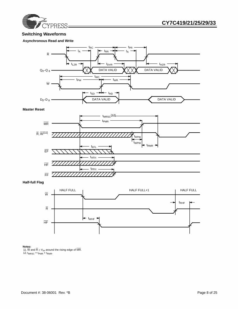
Switching WaveformsAsynchronous Read and Write
Master Reset
Half-full Flag
Notes: 11. W and R ≥ VIH around the rising edge of MR.12. tMRSC = tPMR + tRMR.
DATA VALIDDATA VALID
DATA VALID DATA VALID
tSD tHD
tRC tPRtA tRR tA
tLZR tDVR tHZR
tWCtPW tWR
R
Q0–Q 8
W
D0–D 8
MR
R, W
HF
FF
EF
tMRSCtPMR
tEFL
tHFH
tFFH
tRPW
tWPW tRMR
[11]
[12]
HALF FULL+1HALF FULL HALF FULLW
R
HFtWHF
tRHF
CY7C419/21/25/29/33
Document #: 38-06001 Rev. *B Page 9 of 25
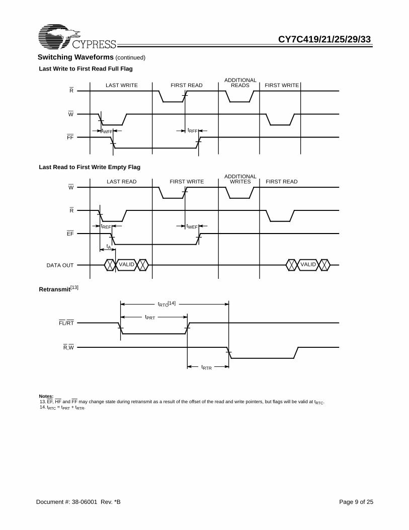
Last Write to First Read Full Flag
Last Read to First Write Empty Flag
Retransmit[13]
Notes: 13. EF, HF and FF may change state during retransmit as a result of the offset of the read and write pointers, but flags will be valid at tRTC.14. tRTC = tPRT + tRTR.
Switching Waveforms (continued)
LAST WRITE FIRST READADDITIONAL
READS FIRST WRITE
tWFF tRFF
R
W
FF
VALID
LAST READ FIRST WRITEADDITIONAL
WRITES FIRST READ
VALID
tREF tWEF
tA
W
R
EF
DATA OUT
tRTC
tPRT
tRTR
FL/RT
R,W
[14]
CY7C419/21/25/29/33
Document #: 38-06001 Rev. *B Page 10 of 25
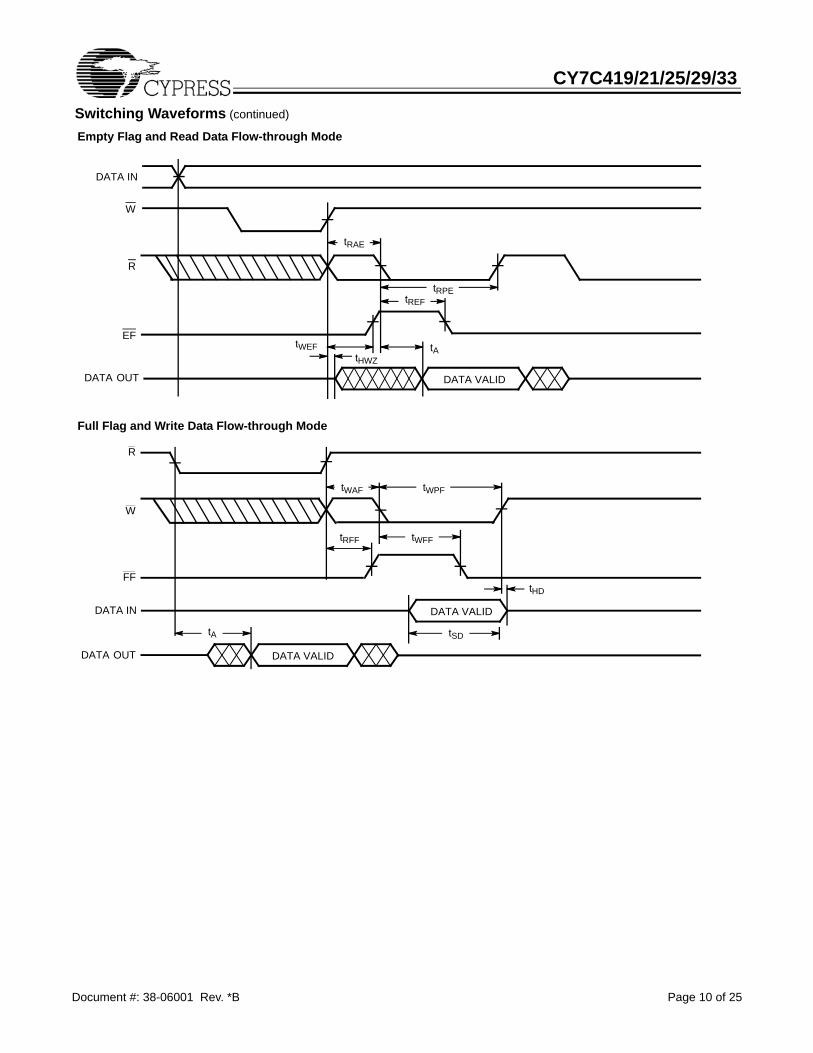
Empty Flag and Read Data Flow-through Mode
Full Flag and Write Data Flow-through Mode
Switching Waveforms (continued)
W
R
EF
DATA IN
DATA OUT DATA VALID
tRAE
tREF
tWEFtHWZ
tA
tRPE
R
W
FF
DATA IN
DATA OUT
DATA VALID
DATA VALID
tWAF tWPF
tWFFtRFF
tSD
tHD
tA
CY7C419/21/25/29/33
Document #: 38-06001 Rev. *B Page 11 of 25
ArchitectureThe CY7C419, CY7C420/1, CY7C424/5, CY7C428/9,CY7C432/3 FIFOs consist of an array of 256, 512, 1024, 2048,4096 words of 9 bits each (implemented by an array ofdual-port RAM cells), a read pointer, a write pointer, controlsignals (W, R, XI, XO, FL, RT, MR), and Full, Half Full, andEmpty flags.
Dual-Port RAMThe dual-port RAM architecture refers to the basic memorycell used in the RAM. The cell itself enables the read and writeoperations to be independent of each other, which isnecessary to achieve truly asynchronous operation of theinputs and outputs. A second benefit is that the time requiredto increment the read and write pointers is much less than thetime that would be required for data propagation through thememory, which would be the case if the memory were imple-mented using the conventional register array architecture.
Resetting the FIFOUpon power-up, the FIFO must be reset with a Master Reset(MR) cycle. This causes the FIFO to enter the empty conditionsignified by the Empty flag (EF) being LOW, and both the HalfFull (HF) and Full flags (FF) being HIGH. Read (R) and write(W) must be HIGH tRPW/tWPW before and tRMR after the risingedge of MR for a valid reset cycle. If reading from the FIFOafter a reset cycle is attempted, the outputs will all be in thehigh-impedance state.
Writing Data to the FIFOThe availability of at least one empty location is indicated by aHIGH FF. The falling edge of W initiates a write cycle. Dataappearing at the inputs (D0–D8) tSD before and tHD after therising edge of W will be stored sequentially in the FIFO.The EF LOW-to-HIGH transition occurs tWEF after the firstLOW-to-HIGH transition of W for an empty FIFO. HF goesLOW tWHF after the falling edge of W following the FIFOactually being Half Full. Therefore, the HF is active once the
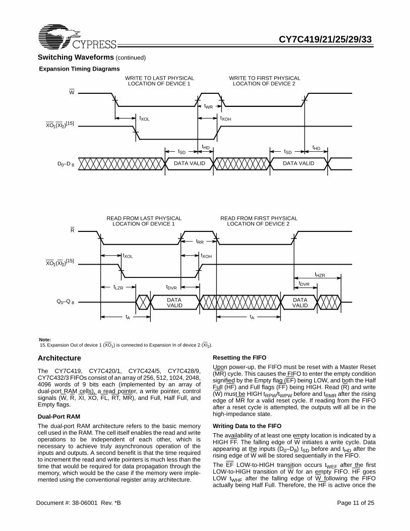
Expansion Timing Diagrams
Note: 15. Expansion Out of device 1 (XO1) is connected to Expansion In of device 2 (XI2).
Switching Waveforms (continued)
R
W
XO1(XI2)
D0–D 8 DATA VALID
DATA DATAVALID VALID
tXOL tXOH
tHDtSD tSD
tHD
tXOL
tLZR
tA
tDVR
tXOH
tA
tDVR
tHZR
XO1(XI2)
Q0–Q 8
WRITE TO LAST PHYSICALLOCATION OF DEVICE 1
WRITE TO FIRST PHYSICALLOCATION OF DEVICE 2
READ FROM LAST PHYSICALLOCATION OF DEVICE 1
READ FROM FIRST PHYSICALLOCATION OF DEVICE 2
tWR
tRR
DATA VALID
[15]
[15]
CY7C419/21/25/29/33
Document #: 38-06001 Rev. *B Page 12 of 25
FIFO is filled to half its capacity plus one word. HF will remainLOW while less than one half of total memory is available forwriting. The LOW-to-HIGH transition of HF occurs tRHF afterthe rising edge of R when the FIFO goes from half full +1 tohalf full. HF is available in standalone and width expansionmodes. FF goes LOW tWFF after the falling edge of W, duringthe cycle in which the last available location is filled. Internallogic prevents overrunning a full FIFO. Writes to a full FIFO areignored and the write pointer is not incremented. FF goesHIGH tRFF after a read from a full FIFO.
Reading Data from the FIFOThe falling edge of R initiates a read cycle if the EF is not LOW.Data outputs (Q0–Q8) are in a high-impedance conditionbetween read operations (R HIGH), when the FIFO is empty,or when the FIFO is not the active device in the depthexpansion mode.When one word is in the FIFO, the falling edge of R initiates aHIGH-to-LOW transition of EF. The rising edge of R causes thedata outputs to go to the high-impedance state and remainsuch until a write is performed. Reads to an empty FIFO areignored and do not increment the read pointer. From the emptycondition, the FIFO can be read tWEF after a valid write.The retransmit feature is beneficial when transferring packetsof data. It enables the receipt of data to be acknowledged bythe receiver and retransmitted if necessary.The Retransmit (RT) input is active in the standalone and widthexpansion modes. The retransmit feature is intended for usewhen a number of writes equal to or less than the depth of theFIFO have occurred since the last MR cycle. A LOW pulse onRT resets the internal read pointer to the first physical locationof the FIFO. R and W must both be HIGH while and tRTR afterretransmit is LOW. With every read cycle after retransmit,previously accessed data as well as not previously accesseddata is read and the read pointer is incremented until it is equalto the write pointer. Full, Half Full, and Empty flags aregoverned by the relative locations of the read and writepointers and are updated during a retransmit cycle. Datawritten to the FIFO after activation of RT are transmitted also.Up to the full depth of the FIFO can be repeatedly retrans-mitted.
Standalone/Width Expansion ModesStandalone and width expansion modes are set by groundingExpansion In (XI) and tying First Load (FL) to VCC. FIFOs canbe expanded in width to provide word widths greater than ninein increments of nine. During width expansion mode, all controlline inputs are common to all devices, and flag outputs fromany device can be monitored.
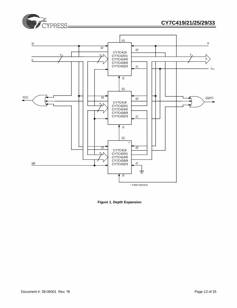
Depth Expansion Mode (see Figure 1)Depth expansion mode is entered when, during a MR cycle,Expansion Out (XO) of one device is connected to ExpansionIn (XI) of the next device, with XO of the last device connectedto XI of the first device. In the depth expansion mode the FirstLoad (FL) input, when grounded, indicates that this part is thefirst to be loaded. All other devices must have this pin HIGH.To enable the correct FIFO, XO is pulsed LOW when the lastphysical location of the previous FIFO is written to and pulsedLOW again when the last physical location is read. Only oneFIFO is enabled for read and one for write at any given time.All other devices are in standby.FIFOs can also be expanded simultaneously in depth andwidth. Consequently, any depth or width FIFO can be createdof word widths in increments of 9. When expanding in depth,a composite FF must be created by ORing the FFs together.Likewise, a composite EF is created by ORing the EFstogether. HF and RT functions are not available in depthexpansion mode.
Use of the Empty and Full FlagsIn order to achieve the maximum frequency, the flags must bevalid at the beginning of the next cycle. However, becausethey can be updated by either edge of the read of write signal,they must be valid by one-half of a cycle. Cypress FIFOs meetthis requirement; some competitors’ FIFOs do not.The reason why the flags are required to be valid by the nextcycle is fairly complex. It has to do with the “effective pulsewidth violation” phenomenon, which can occur at the full andempty boundary conditions, if the flags are not properly used.The empty flag must be used to prevent reading from an emptyFIFO and the full flag must be used to prevent writing into a fullFIFO.For example, consider an empty FIFO that is receiving readpulses. Because the FIFO is empty, the read pulses areignored by the FIFO, and nothing happens. Next, a single wordis written into the FIFO, with a signal that is asynchronous tothe read signal. The (internal) state machine in the FIFO goesfrom empty to empty+1. However, it does this asynchronouslywith respect to the read signal, so that it cannot be determinedwhat the effective pulse width of the read signal is, becausethe state machine does not look at the read signal until it goesto the empty+1 state. In a similar manner, the minimum writepulse width may be violated by attempting to write into a fullFIFO, and asynchronously performing a read. The empty andfull flags are used to avoid these effective pulse width viola-tions, but in order to do this and operate at the maximumfrequency, the flag must be valid at the beginning of the nextcycle.
** 106462 07/11/01 SZV Change from Spec Number: 38-00079 to 38-06001*A 122332 12/30/02 RBI Added power up requirements to maximum ratings information.*B 383597 See ECN PCX Added Pb-Free Logo