Over 60 current and former members of the QSR Research group and 40 members of other HP orgs
esp. Greg Snider, Duncan Stewart, DimitriStrukov, Matthew Pickett, Julien Borghetti, and Jianhua Yang
Our partners at UCLA & Caltech,
Our partners at LBNL and NIST
Supported in part by DARPA & IARPA
IEEE CPMT Chapter, Santa Clara ValleyFebruary 11, 2009
2www.cpmt.org/scv
February 11, 2009 3
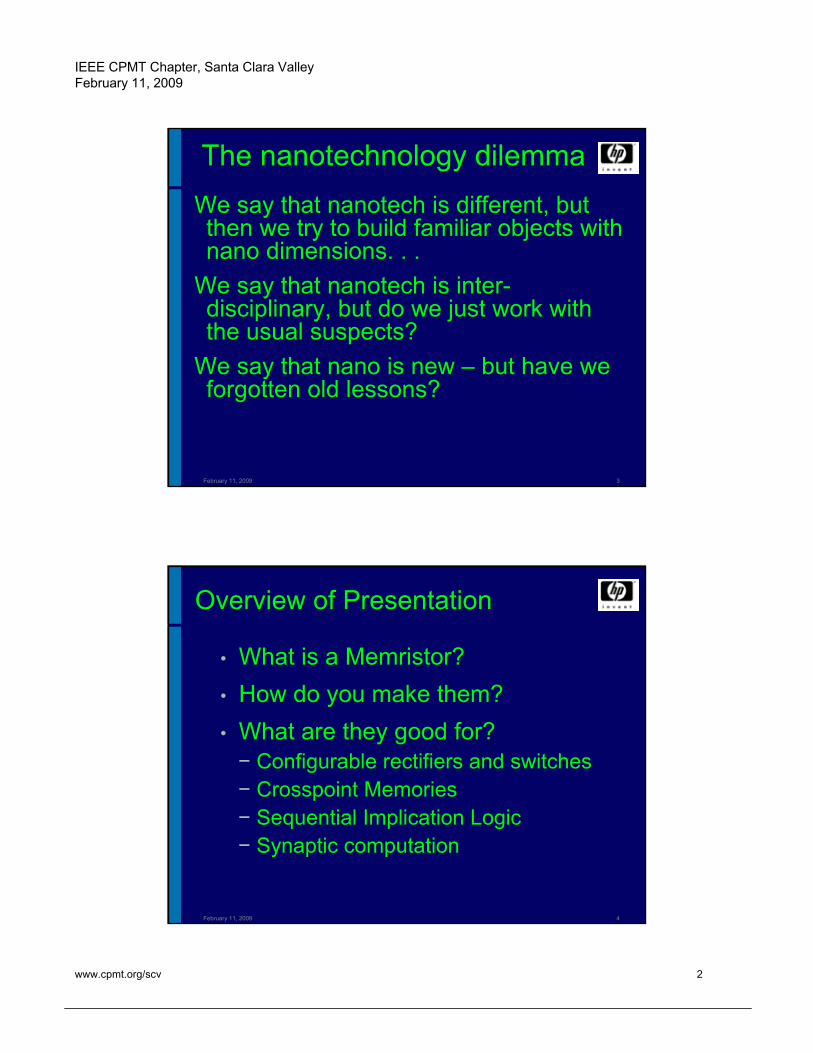
We say that nanotech is different, but then we try to build familiar objects with nano dimensions. . .
We say that nanotech is inter-disciplinary, but do we just work with the usual suspects?
We say that nano is new – but have we forgotten old lessons?
The nanotechnology dilemma
February 11, 2009 4
Overview of Presentation
• What is a Memristor?
• How do you make them?
• What are they good for?− Configurable rectifiers and switches− Crosspoint Memories− Sequential Implication Logic − Synaptic computation
IEEE CPMT Chapter, Santa Clara ValleyFebruary 11, 2009
3www.cpmt.org/scv
February 11, 2009 5
3 fundamental passive linear circuit elements
RESISTORv = R i
CAPACITORq = C v
INDUCTORφ = L i
Capacitor - 1745Volta / von Kleist & van MusschenbroekBenjamin Franklin
Inductor – 1831Michael FaradayJoseph Henry
Resistor – 1827Georg Ohm
February 11, 2009 6
1960’s – Leon Chua generalizes circuit theory to nonlinear systems of equations
RESISTORdv = R di
CAPACITORdq = C dv
INDUCTORdφ = L di
v
i q
And sees that there is a hole where an obvious relation seems to be missing
IEEE CPMT Chapter, Santa Clara ValleyFebruary 11, 2009
4www.cpmt.org/scv
February 11, 2009 7
Realm of linear circuits
Realm of nonlinear circuits
Danger! Chaos!
February 11, 2009 8
Realm of linear circuits
Realm of nonlinear circuits
Nanoelectronics will be nonlinear
Danger! Chaos!
Opportunity!
IEEE CPMT Chapter, Santa Clara ValleyFebruary 11, 2009
5www.cpmt.org/scv
February 11, 2009 9
In1971, Chua postulates the memristor, but states that there is no known example
( )v R w i
( )d w
f id t
L. O. Chua, “Memristor - the missing circuit element,” IEEE Trans. Circuit Theory 18, 507–519 (1971).L. O. Chua and S. M. Kang, "Memristive devices and systems," Proc. IEEE, 64 (2), 209-23 (1976).
RESISTORdv = R,di
CAPACITORdq = C dv
INDUCTORdφ = L di
MEMRISTORdφ = M dq
dq /dt = i
dφ
/dt
= v
i q
v
φ
MEMRISTIVE SYSTEMS
February 11, 2009 10
Four Fundamental Nonlinear Passive Circuit Elements
Resistor
Cu
rren
t
Capacitor
Inductor
Voltage
Cu
rren
t
Memristor
Voltage
dv = R di dq = C dv
dφ = L di dφ = M dq
IEEE CPMT Chapter, Santa Clara ValleyFebruary 11, 2009
6www.cpmt.org/scv
February 11, 2009 11
Current vs. Time for Sinusoidal Voltage Bias
Vo
ltag
e
0
0 0.25 0.5 0.75 1.0
Time
Cu
rren
t
0
Inductance
Capacitance
Resistance
Memristance
February 11, 2009 12
switching… with sharp thresholds
200
150
100
50
0
Cou
nts
(N)
-1.0 -0.5 0.0
Current (mA)
Negative Switching Current60
45
30
15
0
Cou
nts
(N)
1.00.50.0
Voltage (V)
Positive Switching Voltage
-1.0
-0.5
0
0.5
1.0
Cur
rent
(m
A)
-0.5 0 0.5
Voltage (V)
Years of reserch looking for “molecular switches”
M102103A
IEEE CPMT Chapter, Santa Clara ValleyFebruary 11, 2009
7www.cpmt.org/scv
February 11, 2009 13
Pt PtTiO2 TiO2-x
3 nm
2 n
m
O vacancy drift model for TiO2-x switch
Pt PtTiO2 TiO2-x
oxidizedreduced
As fabricated
Positive voltage drifts oxygen vacancies left to increase total conductivity
February 11, 2009 14
Simplified Theory of Memristance
D
TiO2
wV
TiO2-x
ROFF
RON
TiO2:
TiO2-x:
:
A
ROFFRON
Two coupled equations of motion –
One for the charged vacancies
One for the electronic transport
(both versions of Ohm’s law)
ON OFF
( ) ( )( ) 1 ( )
w t w tv t R R i t
D D
)()( ON
V tiD
R
dt
tdw
)(1)(
2ONV
OFF tqD
RRq
M
Nature 453 (2008) 80-83.
IEEE CPMT Chapter, Santa Clara ValleyFebruary 11, 2009
8www.cpmt.org/scv
February 11, 2009 15
• 10ω0
-10
-5
0
5
10
curr
ent
(×10
-3)
-1.0 -0.5 0.0 0.5 1.0
voltage
1.0
0.5
0.0
w/L
0.60.50.40.30.20.10.0
time (×103)
-1.0-0.50.00.51.0
volta
ge
-10-50510
current (×10
-3)
0.60.50.40.30.20.10.0time (×10
3)
1.0
0.5
0.0
w/L
0.60.50.40.30.20.10.0
time (×103)
-1.0-0.50.00.51.0
volta
ge
-8-4048
curre
nt (×10
-3)
0.60.50.40.30.20.10.0time (×10
3)
-8
-4
0
4
8
curr
ent
(×10
-3)
-1.0 -0.5 0.0 0.5 1.0
voltage
0.60.40.20.0
char
ge
500flux
0.60.40.20.0ch
arge
1000flux
• ω0
Look at current-voltage plots of the model
February 11, 2009 16
-1
0
1
volta
ge
1.61.20.80.40.0
1.0
0.5
0.0
w/L
1.61.20.80.40.0time (×10
3)
-1.0
-0.5
0.0
0.5
1.0
curr
ent
-1.0 -0.5 0.0 0.5 1.0voltage
ROFF/RON = 50v0 = 4 VTheory
Pt
TiO2
Pt
Expt
-4
-2
0
2
4
Cur
rent
(m
A)
-1.5 -1.0 -0.5 0.0 0.5 1.0 1.5
Voltage (V)
Comparison between Theory and Experiment:
Pt : TiO2 : Pt Memristor!
IEEE CPMT Chapter, Santa Clara ValleyFebruary 11, 2009
no window function but w is not changing beyond [0, D]
February 11, 2009 18
Metal Oxide Resistive Switches
“Memory effects” in oxideshave been known for a while:
G. Dearnaley et al., Rev. Prog. Phys. (1970):a review with 150+ references
Just a few recent references:metal:
S. Seo et al., APL (2003) NiB. J. Choi et al., JAP (2005) TiH. Sim et al., Microel. Eng. (2005) NbD. Lee et al., EDL (2005) ZrA. Chen et al., IEDM’05 CuM. Kund et al., IEDM’05 AgD. C. Kim et al., APL (2006) NbN. Banno et al., IEICE TE (2006) Cu(S)T.-N. Fang et al., ICMTD’07 CuL. Courtade et al., ICMTD’07 NiW. Guan et al., APL (2007) ZrS.-W. Kim & Y. Nishi, NVMTS’07 Cu(S)D. Stewart, NVMTS’07 TiK.-C. Liu et al., NVMTS’07 HfD. Lee et al., APL (2007) Mo
Per
centa
ge
2.28%
Current (uA)0.005 0.01 0.05 0.1 0.5 1 5 10
15.9%
50.0%
84.1%
97.7%
Per
centa
ge
2.28%
Current (uA)0.005 0.01 0.05 0.1 0.5 1 5 10
15.9%
50.0%
84.1%
97.7%
ONOFF
With time, data are becoming more reproducible:
A. Chen et al. (IEDM’05)
Just a few examples:
B. J. Choi et al. (2005) D. Lee et al. (2007)
-2 0 2 4-20.0µ
-10.0µ
0.0
10.0µ
20.0µ
30.0µ
40.0µ
50.0µ
Cur
ren
t (A
)
Voltage (V)
Ilim set by transistor Vg
OFF-stateVTFL
2
2LeNV t
TFL
ON-state: SCLC with shallow traps
-2 0 2 4-20.0µ
-10.0µ
0.0
10.0µ
20.0µ
30.0µ
40.0µ
50.0µ
Cur
ren
t (A
)
Voltage (V)
Ilim set by transistor Vg
OFF-stateVTFL
2
2LeNV t
TFL
ON-state: SCLC with shallow traps
A. Chen et al. (2005)
Cu
Cu2O
TE
slide courtesy K. Likharev
IEEE CPMT Chapter, Santa Clara ValleyFebruary 11, 2009
10www.cpmt.org/scv
February 11, 2009 19
-
-
-
-
-+
++
+ ++
++
+
+
++
+
+
mobiledonors
fixed acceptors
electronic current
V I
+
Semiconductor memristance is coupled ion-electron motion
February 11, 2009 20
Slightly More Advanced Theory - Ions
diffusion soluteION
driftIONION JJJ
000driftION /sinh EEEqJ
x
NqDJ
diffusion soluteION
)1/()]/(exp[ 32 NaTkUfaD BA N/ t = - JION/ xJION (x = 0) = JION (x = L) = 0
1
exp1
11'Tk
eEE
gNN
B
FD
IEEE CPMT Chapter, Santa Clara ValleyFebruary 11, 2009
11www.cpmt.org/scv
February 11, 2009 21
Slightly More Advanced Theory – e-s
x
xEneJ F
)(
ELELELECTRON
Tk
eEEN
Tk
eEEFNn
B
CFC
TkefEE
B
CFCEL
BCF
exp2/1
ELenezN '20
.
February 11, 2009 22
10
w/ L
0 0.02t / t0
w
time 10
w/ L
0t / t0
0.001
w
NA NA
20 20
Dop
ant
ND(x
)/N
DO 10-1
10-2
10-3
a)
ON to OFF (v = +120v0)
f)
OFF to ON (v = -120v0)
Length x/L 0 Length x/L10 1
ROFF(1-w/L)RON(w/L)
Fie
ld
E/E
0
-500
0c) h)
0
500
10-1
10-2
10-3
0.2
-f/(
EG/e
)
0
10-4 10-3 10-2
time t/t0
10-4 10-3 10-2
time t/t0
0.2
0
g)b)
ROFF(1-w/L)RON(w/L)
IEEE CPMT Chapter, Santa Clara ValleyFebruary 11, 2009
12www.cpmt.org/scv
February 11, 2009 23
Drift-Diffusion Model: Memristance
4
0
-4
-2
2
4
-8
0
-4
-0.4 -0.2 0
1000-100 -50 50
Cur
ren
t J/
J 0
Flux f/f0Cha
rge
q/q 0
(×10
-
3 )Voltage v/v0 = 120 sin[2π(t/t0)/0.01]
February 11, 2009 24
Nano1x17
C
50 nm
Pt
Pt
TiO2
Micro1x1
Micron-devices
1x1
Pt
Bottom electrode
V
V
Ti dioxide
Pt
Top electrode The Workhorse System:
50 nm Pt electrodes by NIL
~3-30 nm TiO2
IEEE CPMT Chapter, Santa Clara ValleyFebruary 11, 2009
13www.cpmt.org/scv
February 11, 2009 25
50 nanometer Pt/TiOx/Pt devices
-200
-100
0
100
200
Cur
rent
(
uA )
-2 -1 0 1 2Voltage ( V )
4
2
0Cur
rent
(
nA )
-2 -1 0 1 2Voltage ( V )
a
b
Virgin I-V
c
50 nm hp
+V turn OFF
-V turn ON
10-3
10-6
10-9
-1 0 1
Pt
Pt
TiO2TiOx
V+
-
~10 ns
~1 us
Switch ON ~10 ns, state is stable for (106?) years
February 11, 2009 26
Vacancy location controls switch polarity
2 0
1 0
0
Cur
rent
(nA
)
- 1 .0 0 .0 1 . 0V o lta g e (V )
I
a
TiO2
Pt
TiOx
Pt
- 1 5
- 1 0
-5
0
Cu
rren
t (n
A)
- 1 .0 0 .0 1 .0V o l ta g e (V )
II
TiOx
Pt
TiO2
Pt
1 0
0
- 1 0
Cur
rent
(m
A)
- 2 -1 0 1V o l ta g e (V )
I’
b
Dio
de
Mem
risto
r
- 1 0
0
1 0
Cur
ren
t (m
A)
210- 1V o l ta g e ( V )
II’
Dio
de
Mem
risto
r
IEEE CPMT Chapter, Santa Clara ValleyFebruary 11, 2009
14www.cpmt.org/scv
February 11, 2009 27
Conclusions on Memristors
• The switching mechanism for the devices is field induced drift of positively charged O vacancies in TiO2 that controls the resistance of the film
• This is the first experimental realization and physical model for a memristor – the fourth nonlinear passive circuit element that has been ‘missing’ for nearly 40 years
• We see that memristance arises naturally in systems where atomic and electronic equations of motion are coupled – this is far more likely to be observed at the nanoscale
February 11, 2009 28
What might memristorsbe used for?
Non-volatile RAMConfig Bits
New forms of logicElectronic Synapse
But need hybrid circuits!
IEEE CPMT Chapter, Santa Clara ValleyFebruary 11, 2009
15www.cpmt.org/scv
February 11, 2009 29
CMOS FPGAs The good:−Massive parallelism−Defect tolerant−Simple design
The bad:−80%-90% area is
wires/configuration−High capacitance
high power
The ugly:−Defect
characterization−Compilation
February 11, 2009 30
SNIC Strategy
Start with CMOS FPGA
IEEE CPMT Chapter, Santa Clara ValleyFebruary 11, 2009
16www.cpmt.org/scv
February 11, 2009 31
SNIC Strategy1. Remove interconnect and configuration bits
February 11, 2009 32
SNIC Strategy1. Remove interconnect
and configuration bits
2. Compress logic
3. Add nano interconnect and configuration
IEEE CPMT Chapter, Santa Clara ValleyFebruary 11, 2009
17www.cpmt.org/scv
February 11, 2009 33
SNIC Strategy1. Remove interconnect
and configuration bits
2. Compress logic
3. Add nano interconnect and configuration
•Inexpensive CMOS design
•Inexpensive process (nanoimprint)
•Nano redundancy defect tolerance
•Small size, high yield low cost
•Low energy
February 11, 2009 34
SNIC: Chip Demo
CMOS layer
Nanowire layer 1
Switching layer
Nanowire layer 2
“via”
Courtesy Qiangfei Xia
IEEE CPMT Chapter, Santa Clara ValleyFebruary 11, 2009