11
1 © 2012 Cadence Design Systems, Inc. All rights reserved. 3D IC WORKING GROUP KEN POTTS 3D IC WORKING GROUP CHAIR

1 © 2012 Cadence Design Systems, Inc. All rights reserved.
3D IC WORKING GROUP
KEN POTTS
3D IC WORKING GROUP CHAIR
2 © 2012 Cadence Design Systems, Inc. All rights reserved.
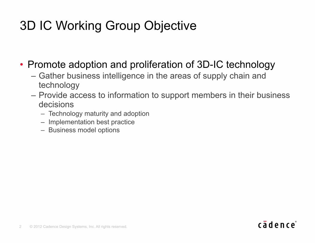
3D IC Working Group Objective
• Promote adoption and proliferation of 3D-IC technology – Gather business intelligence in the areas of supply chain and
technology – Provide access to information to support members in their business
decisions – Technology maturity and adoption – Implementation best practice – Business model options

Ken Potts Group Director, Strategic Marketing Cadence Design Systems
An EDA view of 3DIC

4 © 2012 Cadence Design Systems, Inc. All rights reserved.
3D-IC is a bridge for “More Than Moore” solutions
3D-IC
Source: UBM TechInsights (EETimes, October 2012, May 2011)
5 © 2012 Cadence Design Systems, Inc. All rights reserved.
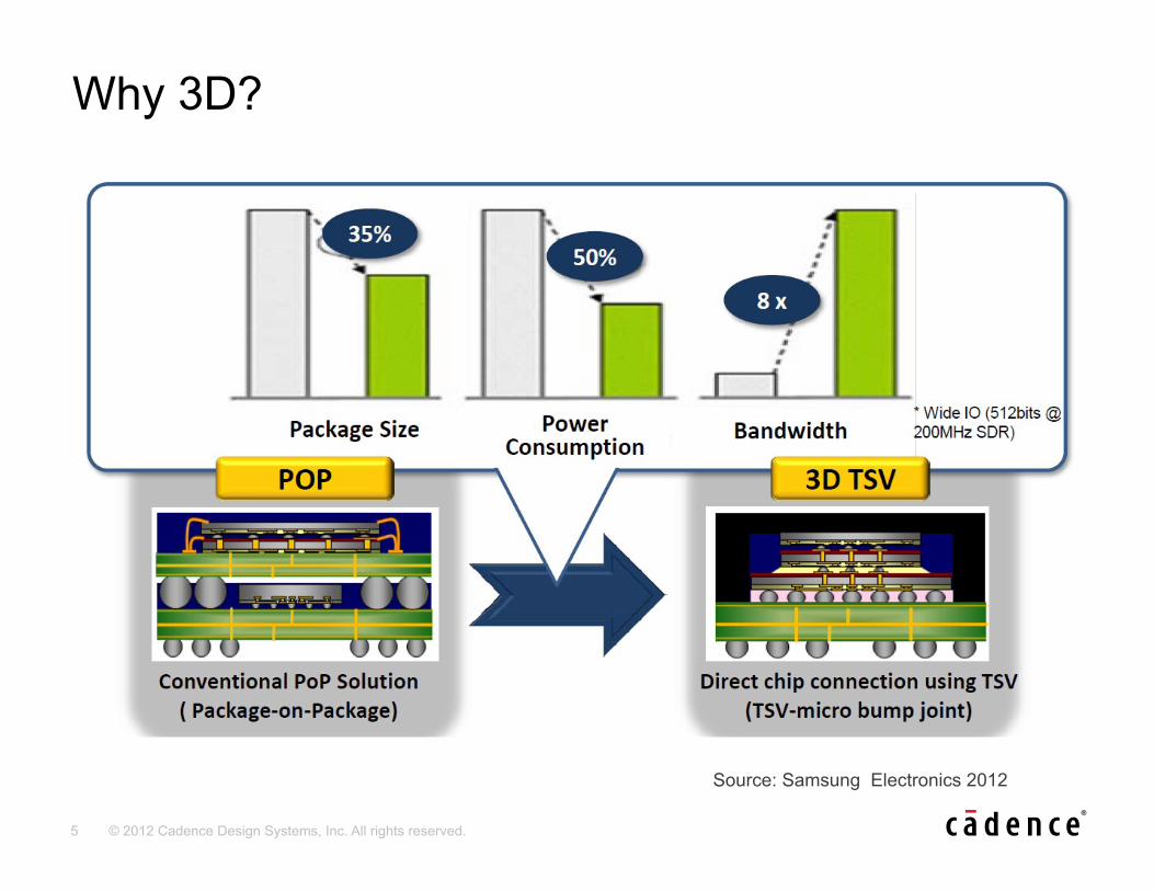
Why 3D?
Source: Samsung Electronics 2012

6 © 2012 Cadence Design Systems, Inc. All rights reserved.
Short-, medium-, and long-term path to 3D-IC EDA work starts at least 3-4 years earlier
Si Partitioning with TSV
Interposer
• Market : FPGA
• Xilinx in 2010
• 2011-2012
Memory Cube with TSVs
• MARKET : Server and computing
• IBM and Micron testchip
• 2012-2013
Logic + memory w/ 2.5D TSV Interposer
• MARKET : GPU, gaming console
• ST testchip in 2010
• 2013-2014
Wide IO + Logic with TSVs
• MARKET : Mobile, tablet, gaming
processors
• ST-E /LETI WIOMING in 2011
• 2013-2014
High-performance
computing
• MARKET : CPU, MCMs etc
• ST-E /LETI WIOMING in 2011
• ~ 2015
SHORT MEDIUM LONG
Standards, ecosystem, cost

7 © 2012 Cadence Design Systems, Inc. All rights reserved.
3DIC Design Flow Challenges 3D Aware Die Floorplan
Optimize power &TSV/Bump locations System Level Exploration Die Implementation
Placement, Optimization and Routing
Multi Die Extraction & Analysis Manage Power, Thermal and SI
DFT for 3DIC Stack & Diagnostics Silicon Package Co-Design
TSV /Bump RDL Routing
Silicon Interposer
Multi-Fabric Planning View
Device Data Source
BGA BGA.txt from Cadence APD
Si Interposer Created on-the-fly
Die Slice 1 LEF / OrbitIO IOview
Die Slice 2 ASCII data
8 © 2012 Cadence Design Systems, Inc. All rights reserved.
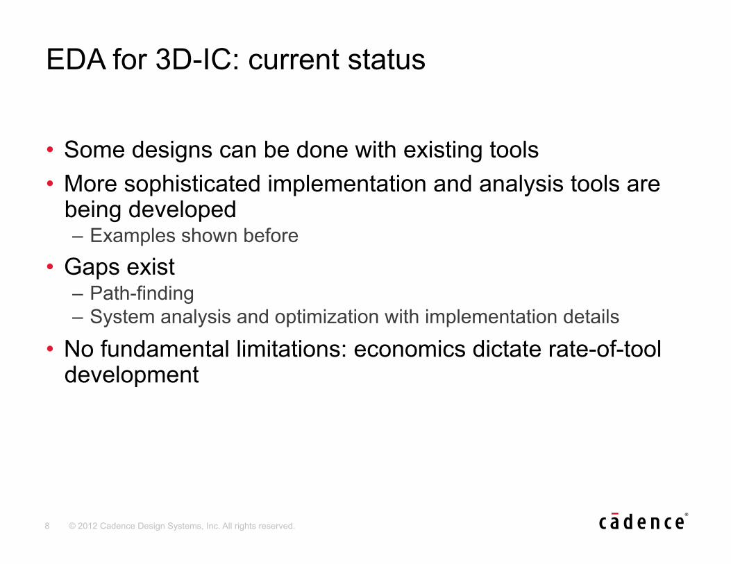
• Some designs can be done with existing tools • More sophisticated implementation and analysis tools are
being developed – Examples shown before
• Gaps exist – Path-finding – System analysis and optimization with implementation details
• No fundamental limitations: economics dictate rate-of-tool development
EDA for 3D-IC: current status

9 © 2012 Cadence Design Systems, Inc. All rights reserved.
• Economical 3D stacking in high-volume manufacturing presents many challenges
• Benefits must exceed the additional costs of TSVs, and yield fallout
• Logistics of testing and assembling die from multiple sources can be substantial
• Mechanical and thermal issues must be addressed
3D integration challenges
10 © 2012 Cadence Design Systems, Inc. All rights reserved.
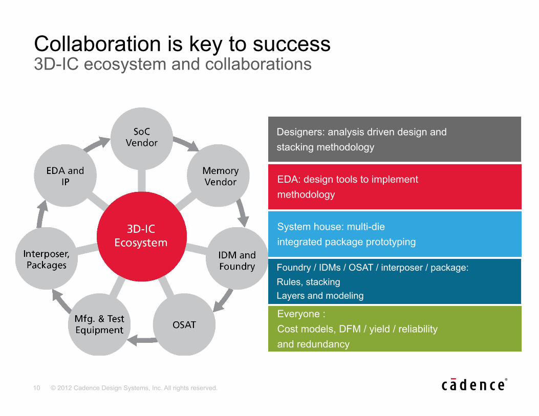
Designers: analysis driven design and stacking methodology
EDA: design tools to implement methodology
System house: multi-die integrated package prototyping
Foundry / IDMs / OSAT / interposer / package: Rules, stacking Layers and modeling
Everyone : Cost models, DFM / yield / reliability and redundancy
Collaboration is key to success 3D-IC ecosystem and collaborations

11 © 2012 Cadence Design Systems, Inc. All rights reserved.


![High-Reliability Accelerometer and Pressure Sensor Design ...meptec.org/Resources/6 - Meggitt.pdf[1] “Practical Understanding of Key Accelerometer Specifications,” Technical Paper](https://static.documents.pub/doc/80x56/5eb59b3291cbaa59696a0fdf/high-reliability-accelerometer-and-pressure-sensor-design-meggittpdf-1.jpg)


![Yole 3DIC & TSV Interconnects July 2012 Sample[1]](https://static.documents.pub/doc/80x56/54650439af795974338b4c77/yole-3dic-tsv-interconnects-july-2012-sample1.jpg)
