37
© 2012 Copyrights © Yole Developpement SA. All rights reserved. 3DIC & TSV interconnects business update Semicon Moscow presentation. Infineon Micron Synopsys VTI CEA LETI Xilinx
© 2012
Copyrights © Yole Developpement SA. All rights reserved.
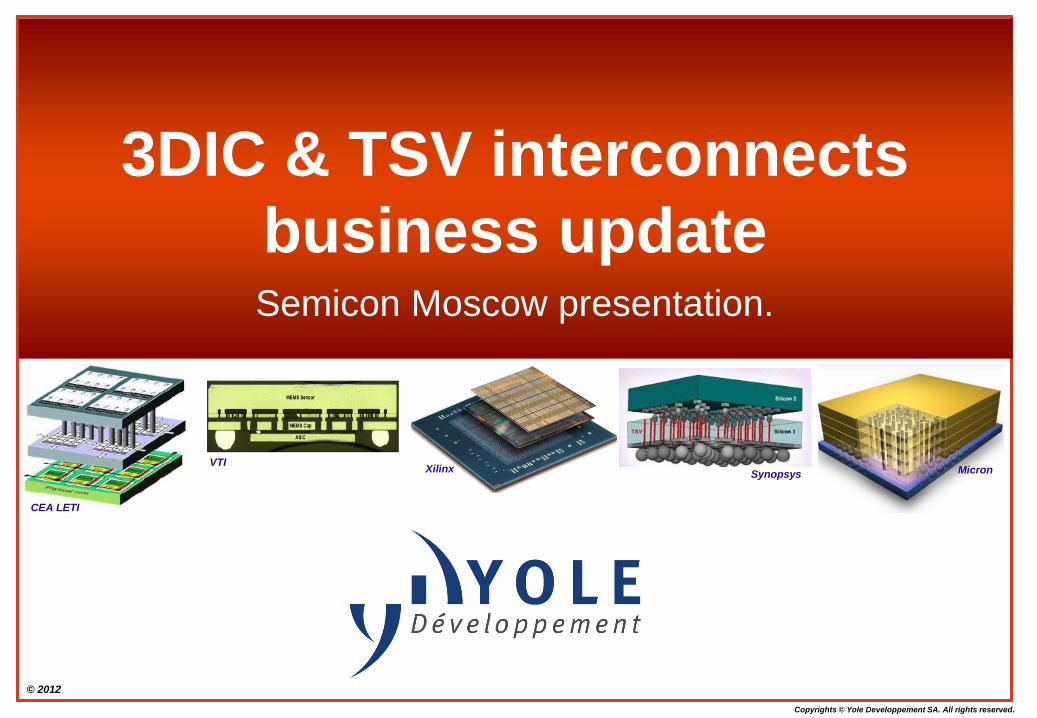
3DIC & TSV interconnects
business update
Semicon Moscow presentation.
Infineon
Micron Synopsys VTI
CEA LETI
Xilinx
© 2012 • 2
Copyrights © Yole Developpement SA. All rights reserved.
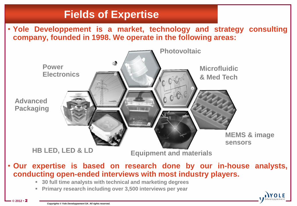
Fields of Expertise
• Yole Developpement is a market, technology and strategy consulting company, founded in 1998. We operate in the following areas:
• Our expertise is based on research done by our in-house analysts, conducting open-ended interviews with most industry players.
30 full time analysts with technical and marketing degrees
Primary research including over 3,500 interviews per year
MEMS & image sensors
Photovoltaic
Advanced Packaging
Microfluidic
& Med Tech
Power Electronics
HB LED, LED & LD Equipment and materials
© 2012 • 3
Copyrights © Yole Developpement SA. All rights reserved.
Mission Statement: Knowledge-Based Company
• Help our customers develop their business through specific
analysis, reports & services providing: Accurate market data, market segmentation and marketing analysis
Technology evaluation; cost estimates and COO analysis
Patent portfolio analysis, licensing strategy and implementation
Identification of strategic development opportunities for companies and business units
Support for M&A, due diligence, and identifying new investors
Advertising opportunities in YOLE magazines, webcasts and specific events
• You get operational results from Yole analysis and actions
© 2012 • 4
Copyrights © Yole Developpement SA. All rights reserved.
4 Business Models
• Custom Analysis: Largest part of Yole activities
Covered by NDA agreement
A few days to several months of work, depending on objectives
• Published Reports: An average of 40 reports published every year
Available individually or through Annual Subscription Program
Market and technology reports, Patent analysis, Reverse Engineering/Costing reports and Reverse Costing tools
• i-Micronews Media: Newsletters and webcasts on 3D, MEMS, Power electronics, LED and imaging
Advertising services providing access to our 45 000+ subscribers to be visible and diffuse information on your company and products
• Yole Finance services:
M&A (buying and selling)
Due diligence
Fund-raising services
© 2012 • 5
Copyrights © Yole Developpement SA. All rights reserved.
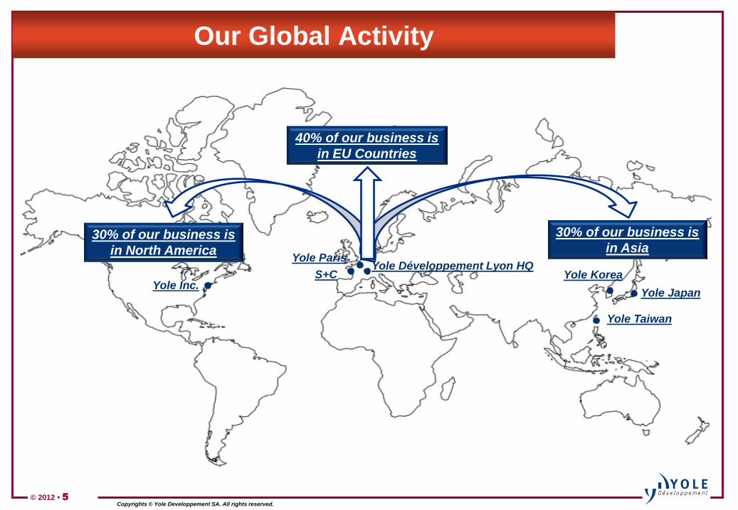
Our Global Activity
Yole Inc.
Yole Paris
Yole Japan
30% of our business is
in North America
30% of our business is
in Asia
40% of our business is
in EU Countries
Yole Korea Yole Développement Lyon HQ
Yole Taiwan
S+C
© 2012 • 6
Copyrights © Yole Developpement SA. All rights reserved.
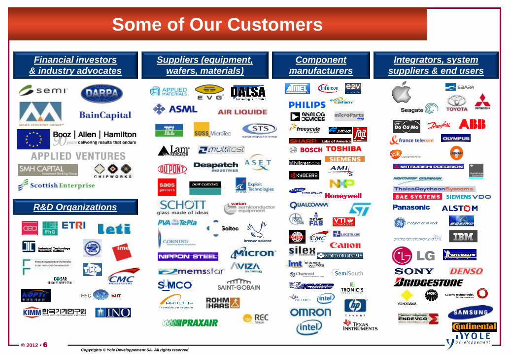
Some of Our Customers
Financial investors
& industry advocates
R&D Organizations
Suppliers (equipment,
wafers, materials)
Component
manufacturers
Integrators, system
suppliers & end users
© 2012 • 7
Copyrights © Yole Développement SA. All rights reserved.
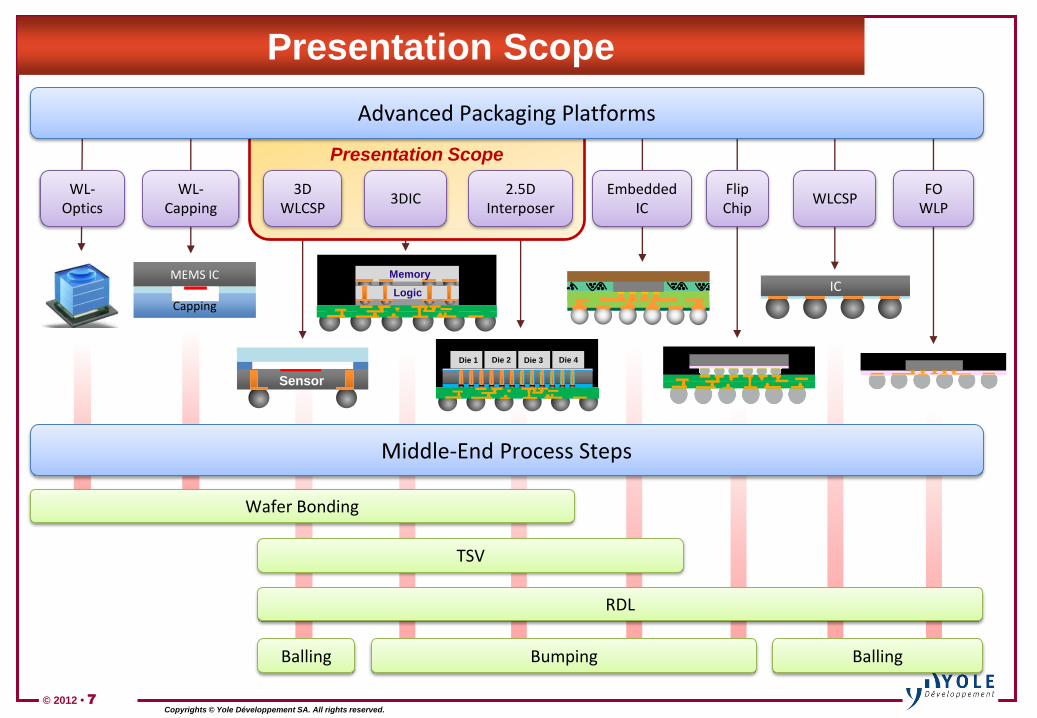
Presentation Scope
Advanced Packaging Platforms
RDL
Bumping Balling
Wafer Bonding
TSV
WL-Optics
WL-Capping
2.5D Interposer
3DIC
Balling
WLCSP FO
WLP Embedded
IC Flip Chip
MEMS IC
Capping
IC
Sensor
Memory
Logic
3D WLCSP
Die 1 Die 2 Die 3 Die 4
Middle-End Process Steps
Presentation Scope
© 2012 • 8
Copyrights © Yole Developpement SA. All rights reserved.
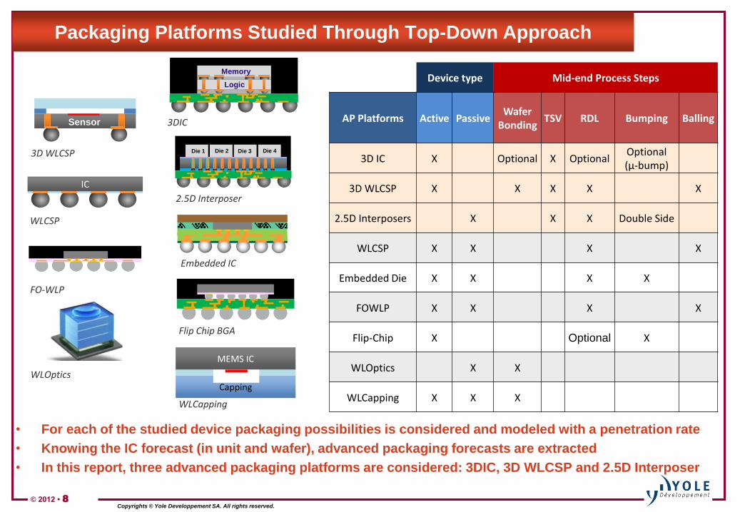
Packaging Platforms Studied Through Top-Down Approach
• For each of the studied device packaging possibilities is considered and modeled with a penetration rate
• Knowing the IC forecast (in unit and wafer), advanced packaging forecasts are extracted
• In this report, three advanced packaging platforms are considered: 3DIC, 3D WLCSP and 2.5D Interposer
Device type Mid-end Process Steps
AP Platforms Active Passive Wafer
Bonding TSV RDL Bumping Balling
3D IC X Optional X Optional Optional (µ-bump)
3D WLCSP X X X X X
2.5D Interposers X X X Double Side
WLCSP X X X X
Embedded Die X X X X
FOWLP X X X X
Flip-Chip X Optional X
WLOptics X X
WLCapping X X X
MEMS IC
Capping
IC
Sensor 3DIC
3D WLCSP
WLCSP
FO-WLP
WLOptics
2.5D Interposer
Embedded IC
Flip Chip BGA
WLCapping
Memory
Logic
Die 1 Die 2 Die 3 Die 4
© 2012 • 9
Copyrights © Yole Développement SA. All rights reserved.
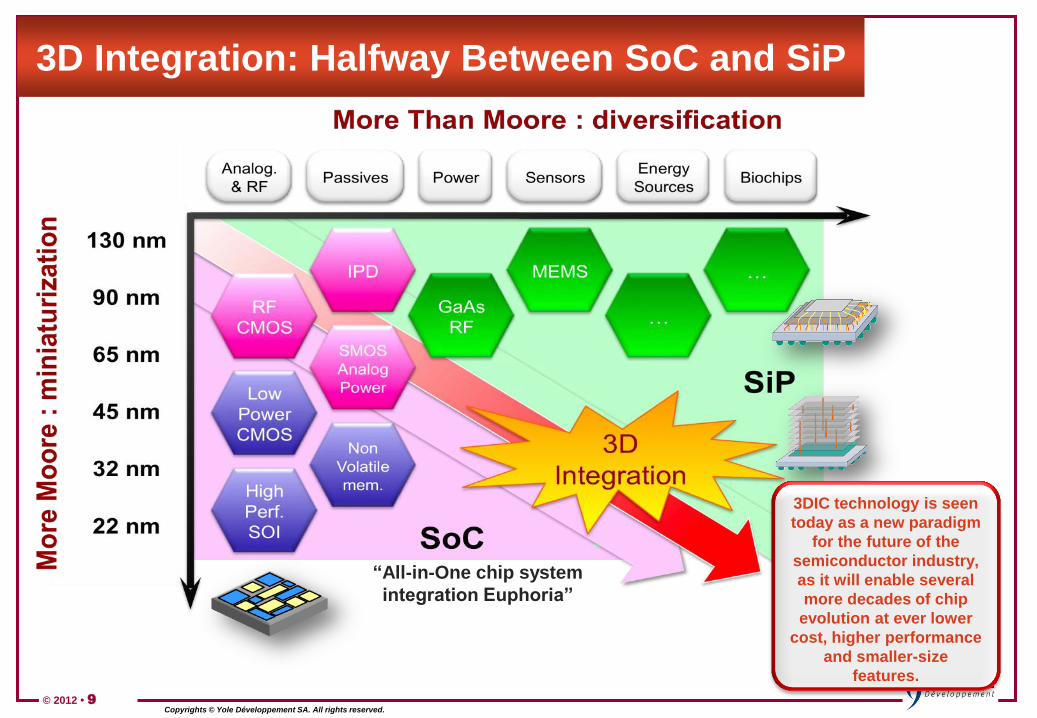
3D Integration: Halfway Between SoC and SiP
“All-in-One chip system
integration Euphoria”
3DIC technology is seen
today as a new paradigm
for the future of the
semiconductor industry,
as it will enable several
more decades of chip
evolution at ever lower
cost, higher performance
and smaller-size
features.
© 2012 • 10
Copyrights © Yole Développement SA. All rights reserved.
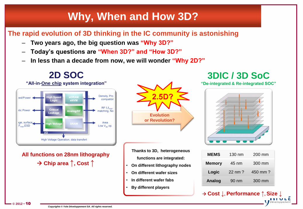
Why, When and How 3D?
The rapid evolution of 3D thinking in the IC community is astonishing
– Two years ago, the big question was “Why 3D?”
– Today‟s questions are “When 3D?” and “How 3D?”
– In less than a decade from now, we will wonder “Why 2D?”
Evolution
or Revolution?
3DIC / 3D SoC “De-integrated & Re-integrated SOC”
2D SOC “All-in-One chip system integration”
All functions on 28nm lithography
Chip area ↑, Cost ↑
MEMS 130 nm 200 mm
Memory 45 nm 300 mm
Logic 22 nm ? 450 mm ?
Analog 90 nm 300 mm
Thanks to 3D, heterogeneous
functions are integrated:
• On different lithography nodes
• On different wafer sizes
• In different wafer fabs
• By different players
Cost ↓, Performance ↑, Size ↓
© 2012 • 11
Copyrights © Yole Développement SA. All rights reserved.
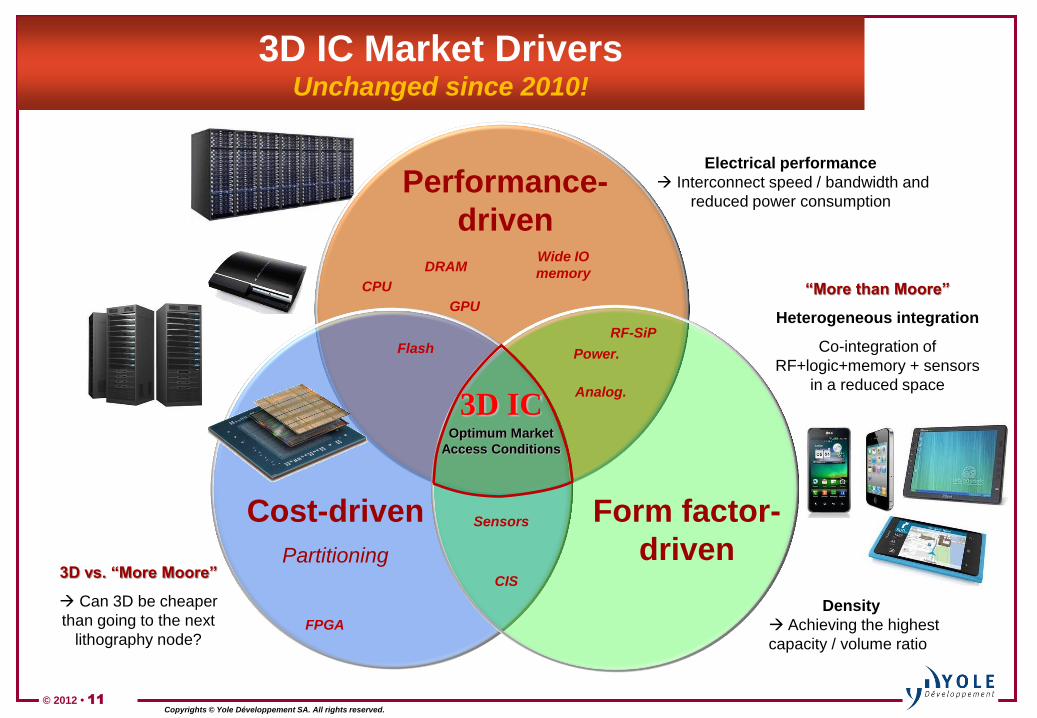
“More than Moore”
Heterogeneous integration
Co-integration of
RF+logic+memory + sensors
in a reduced space
Density
Achieving the highest
capacity / volume ratio
Form factor-
driven
Performance-
driven
3D IC Optimum Market
Access Conditions
Wide IO
memory
CIS
DRAM
RF-SiP
Electrical performance
Interconnect speed / bandwidth and
reduced power consumption
3D vs. “More Moore”
Can 3D be cheaper
than going to the next
lithography node?
Flash
Cost-driven
Partitioning
Sensors
3D IC Market Drivers Unchanged since 2010!
CPU
GPU
Power.
Analog.
FPGA
© 2012
Copyrights © Yole Developpement SA. All rights reserved.
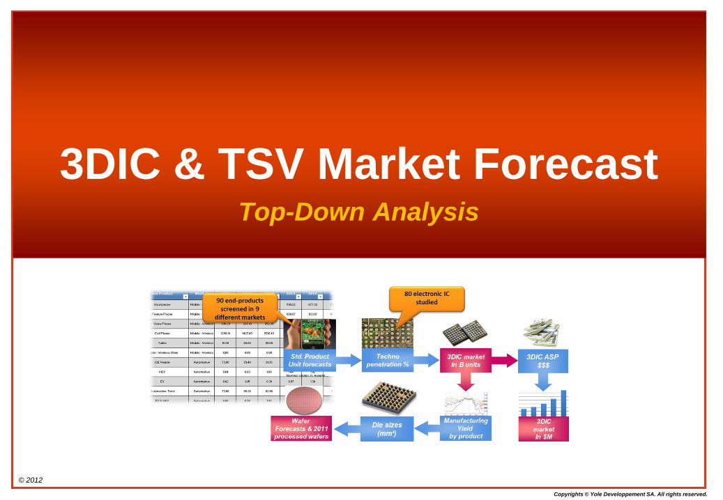
3DIC & TSV Market Forecast Top-Down Analysis
© 2012 • 13
Copyrights © Yole Developpement SA. All rights reserved.
-
2.000.000
4.000.000
6.000.000
8.000.000
10.000.000
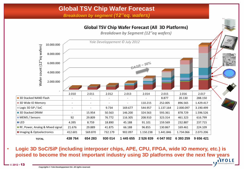
2.010 2.011 2.012 2.013 2.014 2.015 2.016 2.017
3D Stacked NAND Flash - - - - - 8.877 20.130 288.150
3D Wide IO Memory - - - - 110.215 252.005 896.565 1.429.417
Logic 3D SiP / SoC - - 9.734 169.677 544.957 1.137.164 2.000.097 3.190.499
3D Stacked DRAM - 15.954 50.563 146.200 324.563 593.361 878.729 1.596.526
MEMS / Sensors 92 29.809 76.772 116.305 208.910 323.314 461.323 616.799
LED 4.395 8.759 18.890 45.188 91.101 159.569 232.887 237.715
RF, Power, Analog & Mixed signal 21.676 29.889 41.875 66.188 96.855 130.867 169.461 224.109
Imaging & Optoelectronics 412.601 569.870 732.179 902.097 1.150.238 1.441.846 1.734.066 2.073.206
Waf
er c
ou
nt
(12
’’eq
waf
ers)
Global TSV Chip Wafer Forecast (All 3D Platforms) Breakdown by Segment (12''eq wafers)
Yole Developpement © July 2012
Global TSV Chip Wafer Forecast Breakdown by segment (12’’eq. wafers)
• Logic 3D SoC/SiP (including interposer chips, APE, CPU, FPGA, wide IO memory, etc.) is
poised to become the most important industry using 3D platforms over the next few years
TOTAL 438 764 654 283 930 014 1 445 655 2 526 839 4 047 002 6 393 259 9 656 421
© 2012 • 14
Copyrights © Yole Développement SA. All rights reserved.
0
20
40
60
80
100
120
140
Rev
enu
es (
M$
)
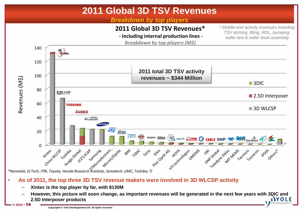
2011 Global 3D TSV Revenues* - Including internal production lines -
Breakdown by top players (M$)
3DIC
2.5D Interposer
3D WLCSP
*Nemotek, Q-Tech, ITRI, Toyota, Honda Research Institute, Sematech, UMC, Toshiba, TI
2011 Global 3D TSV Revenues Breakdown by top players
• As of 2011, the top three 3D TSV revenue makers were involved in 3D WLCSP activity
– Xintec is the top player by far, with $130M
– However, this picture will soon change, as important revenues will be generated in the next few years with 3DIC and
2.5D Interposer products
* Middle-end activity revenues including
TSV etching, filling, RDL, bumping,
wafer test & wafer level assembly
2011 total 3D TSV activity
revenues ~ $344 Million

© 2012 • 15
Copyrights © Yole Developpement SA. All rights reserved.
3D WLCSP: the Most Mature 3D TSV Platform
• 3D WLCSP is the preferred solution today for the efficient assembly of small-size optoelectronic
chips, like CMOS image sensors. It is also the most mature 3D TSV platform at the moment, as we
estimate the market to be ~ $272M in 2011 for the “middle-end” processing factories serving this
specific market
Xintec $130,0M
48%
China WLCSP $66,0M
24%
Toshiba $26,7M
10%
JCAP $21.6M
8%
Samsung $18,2M
7%
STMicroelectronics $2,3M
1% Others* $5,3M
2%
2011 3D WLCSP Platform Middle-End Revenues* Including internal production lines
Breakdown by top players (M$)
Yole Developpement © July 2012
* Middle -end activity revenues including TSV
etching, filling, RDL, bumping, wafer test & wafer level assembly
Total =
$272M
*Others = Oki, G-MEMS,
Nemotek, Q-Tech
© 2012 • 16
Copyrights © Yole Developpement SA. All rights reserved.
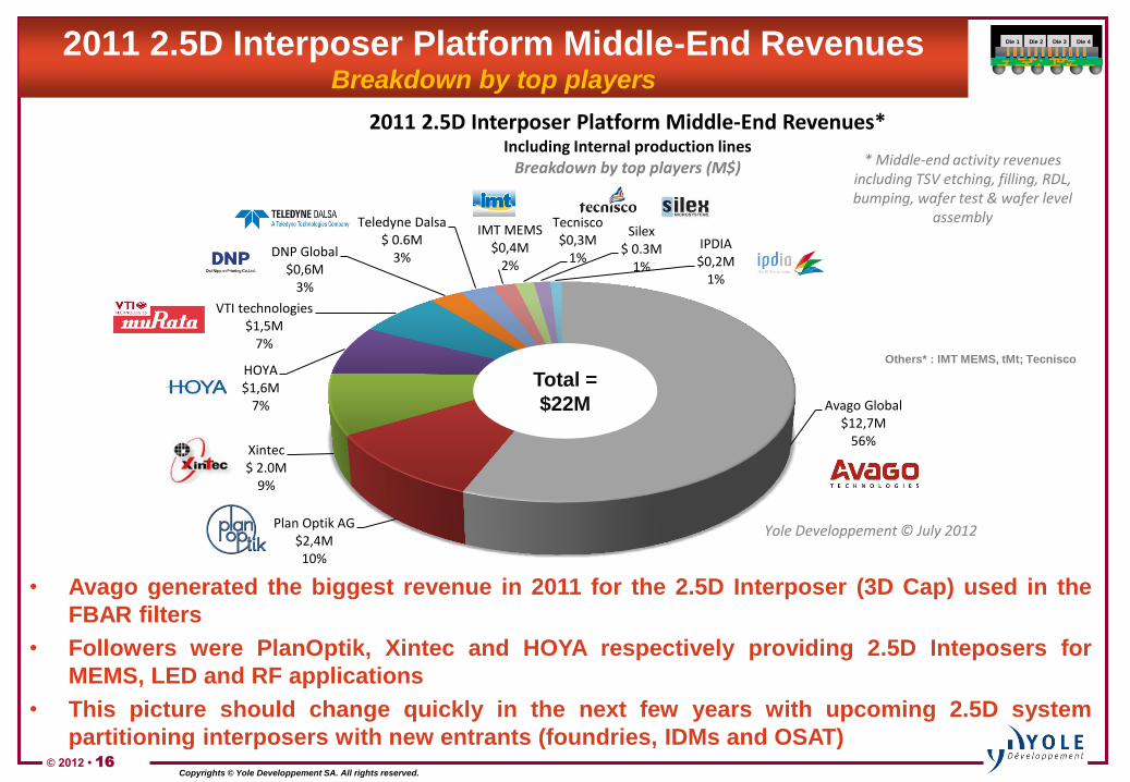
• Avago generated the biggest revenue in 2011 for the 2.5D Interposer (3D Cap) used in the
FBAR filters
• Followers were PlanOptik, Xintec and HOYA respectively providing 2.5D Inteposers for
MEMS, LED and RF applications
• This picture should change quickly in the next few years with upcoming 2.5D system
partitioning interposers with new entrants (foundries, IDMs and OSAT)
Avago Global $12,7M
56%
Plan Optik AG $2,4M 10%
Xintec $ 2.0M
9%
HOYA $1,6M
7%
VTI technologies $1,5M
7%
DNP Global $0,6M
3%
Teledyne Dalsa $ 0.6M
3%
IMT MEMS $0,4M
2%
Tecnisco $0,3M
1%
Silex $ 0.3M
1%
IPDIA $0,2M
1%
2011 2.5D Interposer Platform Middle-End Revenues* Including Internal production lines
Breakdown by top players (M$)
Yole Developpement © July 2012
* Middle-end activity revenues including TSV etching, filling, RDL, bumping, wafer test & wafer level
assembly
2011 2.5D Interposer Platform Middle-End Revenues Breakdown by top players
Total =
$22M
Others* : IMT MEMS, tMt; Tecnisco
Die 1 Die 2 Die 3 Die 4
© 2012 • 17
Copyrights © Yole Développement SA. All rights reserved.
The Future 3DIC Market is Driven
by Stacked Memories & Logic SOC Applications
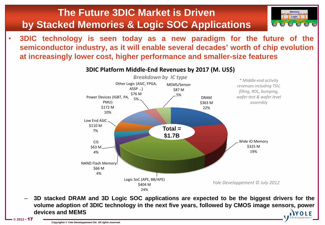
• 3DIC technology is seen today as a new paradigm for the future of the
semiconductor industry, as it will enable several decades‟ worth of chip evolution
at increasingly lower cost, higher performance and smaller-size features
– 3D stacked DRAM and 3D Logic SOC applications are expected to be the biggest drivers for the
volume adoption of 3DIC technology in the next five years, followed by CMOS image sensors, power
devices and MEMS
DRAM $363 M
22%
Wide IO Memory $325 M
19%
Logic SoC (APE, BB/APE) $404 M
24%
NAND Flash Memory $66 M
4%
CIS $63 M
4%
Low End ASIC $110 M
7%
Power Devices (IGBT, PA, PMU)
$172 M 10%
Other Logic (ASIC, FPGA, ASSP …) $76 M
5%
MEMS/Sensor $87 M
5%
3DIC Platform Middle-End Revenues by 2017 (M. US$) Breakdown by IC type
* Middle-end activity revenues including TSV, filling, RDL, bumping,
wafer test & wafer level assembly
Yole Developpement © July 2012
Total =
$1.7B
Memory
Logic
© 2012
Copyrights © Yole Developpement SA. All rights reserved.
Infrastructure
&
Supply Chain Analysis
© 2012 • 19
Copyrights © Yole Développement SA. All rights reserved.
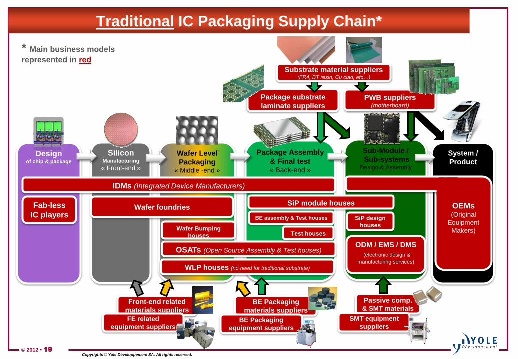
Traditional IC Packaging Supply Chain*
System /
Product
Sub-Module /
Sub-systems Design & Assembly
Design of chip & package
Wafer Level
Packaging « Middle -end »
Silicon Manufacturing
« Front-end »
Package Assembly
& Final test « Back-end »
Front-end related
materials suppliers
OEMs (Original
Equipment
Makers)
FE related
equipment suppliers
BE Packaging
materials suppliers
BE Packaging
equipment suppliers
Fab-less
IC players
IDMs (Integrated Device Manufacturers)
Wafer foundries
OSATs (Open Source Assembly & Test houses)
Wafer Bumping
houses
BE assembly & Test houses
PWB suppliers (motherboard)
ODM / EMS / DMS
(electronic design &
manufacturing services)
SiP module houses
Passive comp. & SMT materials
SMT equipment
suppliers
SiP design
houses
Test houses
Package substrate
laminate suppliers
Substrate material suppliers (FR4, BT resin, Cu clad, etc…)
* Main business models
represented in red
WLP houses (no need for traditional substrate)
© 2012 • 20
Copyrights © Yole Développement SA. All rights reserved.
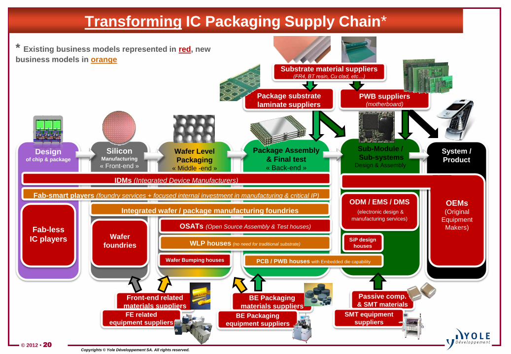
Transforming IC Packaging Supply Chain*
System /
Product
Sub-Module /
Sub-systems Design & Assembly
Design of chip & package
Wafer Level
Packaging « Middle -end »
Silicon Manufacturing
« Front-end »
Package Assembly
& Final test « Back-end »
Front-end related
materials suppliers
OEMs (Original
Equipment
Makers)
FE related
equipment suppliers
BE Packaging
materials suppliers
BE Packaging
equipment suppliers
Fab-less
IC players
IDMs (Integrated Device Manufacturers)
Integrated wafer / package manufacturing foundries
OSATs (Open Source Assembly & Test houses)
WLP houses (no need for traditional substrate)
PWB suppliers (motherboard)
ODM / EMS / DMS
(electronic design &
manufacturing services)
Passive comp. & SMT materials
SMT equipment
suppliers
SiP design
houses
Package substrate
laminate suppliers
Substrate material suppliers (FR4, BT resin, Cu clad, etc…)
* Existing business models represented in red, new
business models in orange
Wafer
foundries
Fab-smart players (foundry services + focused internal investment in manufacturing & critical IP)
Wafer Bumping houses PCB / PWB houses with Embedded die capability
© 2012 • 21
Copyrights © Yole Développement SA. All rights reserved.
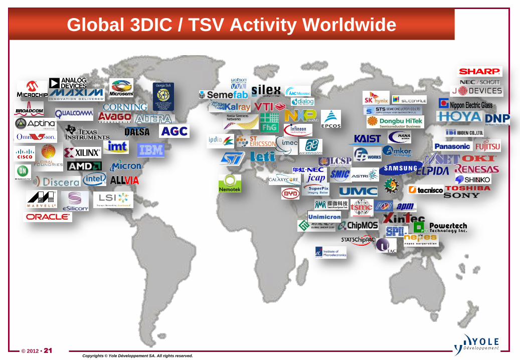
Global 3DIC / TSV Activity Worldwide
© 2012
Copyrights © Yole Developpement SA. All rights reserved.
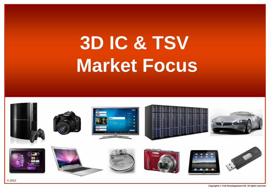
3D IC & TSV
Market Focus
© 2012 • 23
Copyrights © Yole Développement SA. All rights reserved.
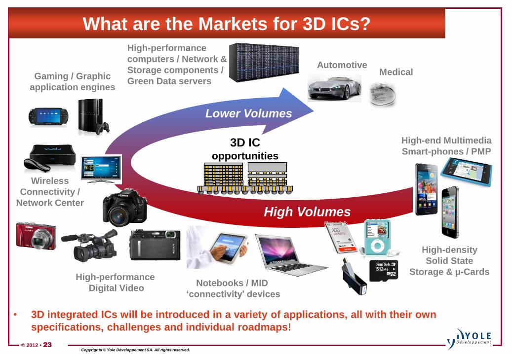
What are the Markets for 3D ICs?
• 3D integrated ICs will be introduced in a variety of applications, all with their own
specifications, challenges and individual roadmaps!
High Volumes
Lower Volumes
3D IC opportunities
High-end Multimedia
Smart-phones / PMP
High-density
Solid State
Storage & µ-Cards
Notebooks / MID
„connectivity‟ devices
Gaming / Graphic
application engines
High-performance
computers / Network &
Storage components /
Green Data servers
High-performance
Digital Video
Wireless
Connectivity /
Network Center
Automotive Medical
© 2012 • 24
Copyrights © Yole Développement SA. All rights reserved.
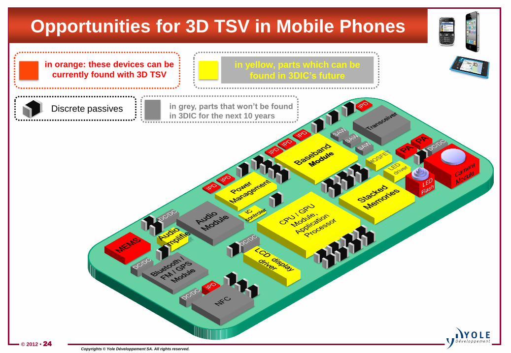
Opportunities for 3D TSV in Mobile Phones
in orange: these devices can be
currently found with 3D TSV in yellow, parts which can be
found in 3DIC‟s future
Discrete passives in grey, parts that won‟t be found
in 3DIC for the next 10 years
© 2012 • 25
Copyrights © Yole Développement SA. All rights reserved.
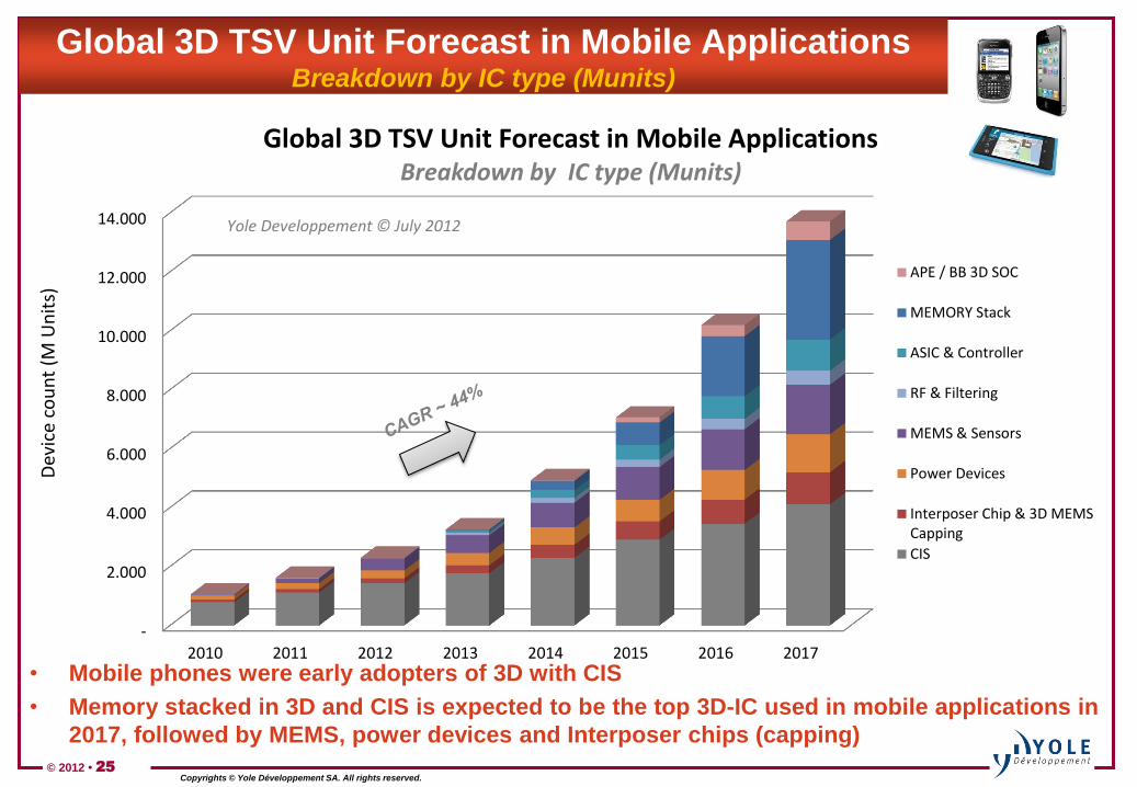
Global 3D TSV Unit Forecast in Mobile Applications Breakdown by IC type (Munits)
• Mobile phones were early adopters of 3D with CIS
• Memory stacked in 3D and CIS is expected to be the top 3D-IC used in mobile applications in
2017, followed by MEMS, power devices and Interposer chips (capping)
-
2.000
4.000
6.000
8.000
10.000
12.000
14.000
2010 2011 2012 2013 2014 2015 2016 2017
Dev
ice
cou
nt
(M U
nit
s)
Global 3D TSV Unit Forecast in Mobile Applications Breakdown by IC type (Munits)
APE / BB 3D SOC
MEMORY Stack
ASIC & Controller
RF & Filtering
MEMS & Sensors
Power Devices
Interposer Chip & 3D MEMSCapping
CIS
Yole Developpement © July 2012
© 2012 • 26
Copyrights © Yole Développement SA. All rights reserved.
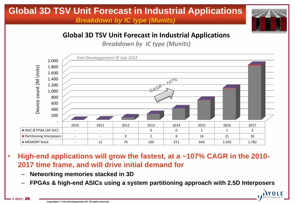
Global 3D TSV Unit Forecast in Industrial Applications Breakdown by IC type (Munits)
• High-end applications will grow the fastest, at a ~107% CAGR in the 2010-
2017 time frame, and will drive initial demand for
– Networking memories stacked in 3D
– FPGAs & high-end ASICs using a system partitioning approach with 2.5D Interposers
-
200
400
600
800
1.000
1.200
1.400
1.600
1.800
2.000
2010 2011 2012 2013 2014 2015 2016 2017
ASIC & FPGA (3D SoC) - - - 0 0 1 1 3
Partitioning Interposers - - 0 2 8 14 21 30
MEMORY Stack - 12 79 190 371 649 1.035 1.782
Dev
ice
cou
nt
(M U
nit
s)
Global 3D TSV Unit Forecast in Industrial Applications Breakdown by IC type (Munits)
Yole Developpement © July 2012
© 2012
Copyrights © Yole Développement SA. All rights reserved.
3D IC & TSV
Application Focus
© 2012 • 28
Copyrights © Yole Développement SA. All rights reserved.
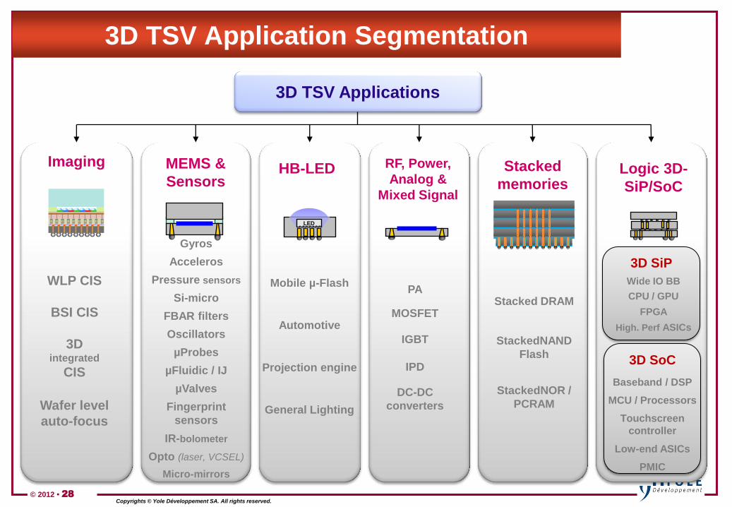
3D TSV Application Segmentation
Imaging
LED
MEMS &
Sensors HB-LED Stacked
memories
RF, Power,
Analog &
Mixed Signal
Logic 3D-
SiP/SoC
3D TSV Applications
WLP CIS
BSI CIS
Wafer level
auto-focus
3D integrated
CIS
Gyros
Acceleros
Pressure sensors
Si-micro
FBAR filters
Oscillators
µProbes
µFluidic / IJ
µValves
Fingerprint
sensors
Micro-mirrors
IR-bolometer
Opto (laser, VCSEL)
Mobile µ-Flash
Automotive
General Lighting
Projection engine
PA
MOSFET
IGBT
IPD
DC-DC
converters
Stacked DRAM
StackedNAND
Flash
StackedNOR /
PCRAM
3D SoC
Baseband / DSP
MCU / Processors
Touchscreen
controller
Low-end ASICs
PMIC
3D SiP
Wide IO BB
CPU / GPU
FPGA
High. Perf ASICs
© 2012 • 29
Copyrights © Yole Développement SA. All rights reserved.
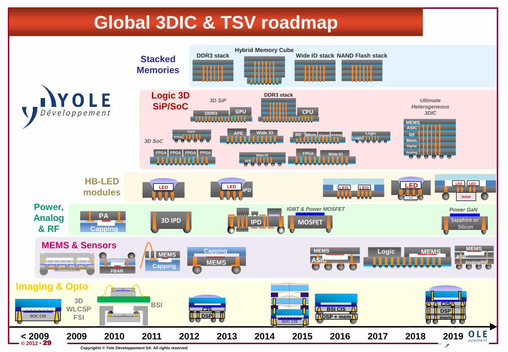
PA
Capping IPD Sapphire or
Silicon 3D IPD MOSFET
IGBT & Power MOSFET Power GaN
2012 2014 2016 2018
CIS DSP SOC CIS
BSI CIS
DSP + mem DSP
mem
CIS
SOC CIS
SOC CIS
2010
SOC CIS
2011 2013 2015 2017 2019
3D
WLCSP
FSI
BSI
< 2009 2009
MEMS
ASIC MEMS
Capping
MEMS
ASIC Analog/RF
MEMS Logic
MEMS
Capping
FBAR
Capping
DDR3 stack Hybrid Memory Cube
NAND Flash stack Wide IO stack
LED
Driver
LED
Driver
LED LED
LED LED LED IPD
FPGA FPGA FPGA FPGA
Analog Digital RF Mem. Analog
Digital
ASIC MEMS
Analog
Digital
RF
Mem.
Wide IO FPGA
Wide IO APE
Wide IO
APE
CPU
DDR3 stack
GPU DDR3
Logic
Logic
Logic 3D
SiP/SoC
Global 3DIC & TSV roadmap
MEMS & Sensors
Imaging & Opto
Power,
Analog
& RF
Stacked
Memories
HB-LED
modules
3D SoC
3D SiP Ultimate
Heterogeneous
3DIC
© 2012 • 30
Copyrights © Yole Développement SA. All rights reserved.
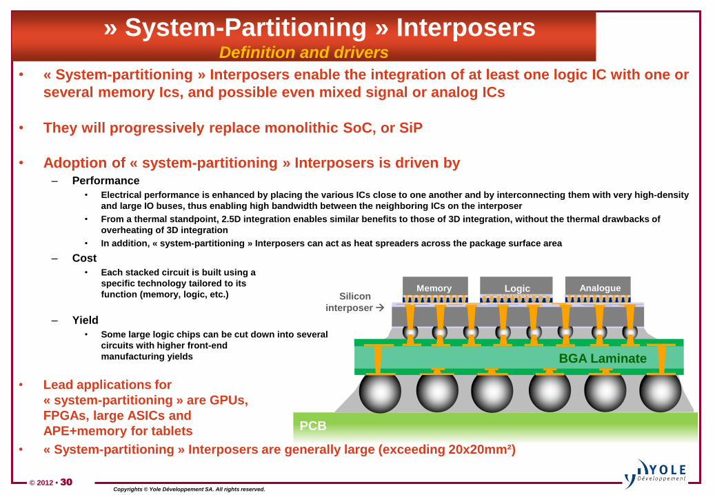
» System-Partitioning » Interposers Definition and drivers
• « System-partitioning » Interposers enable the integration of at least one logic IC with one or
several memory Ics, and possible even mixed signal or analog ICs
• They will progressively replace monolithic SoC, or SiP
• Adoption of « system-partitioning » Interposers is driven by – Performance
• Electrical performance is enhanced by placing the various ICs close to one another and by interconnecting them with very high-density
and large IO buses, thus enabling high bandwidth between the neighboring ICs on the interposer
• From a thermal standpoint, 2.5D integration enables similar benefits to those of 3D integration, without the thermal drawbacks of
overheating of 3D integration
• In addition, « system-partitioning » Interposers can act as heat spreaders across the package surface area
– Cost
• Each stacked circuit is built using a
specific technology tailored to its
function (memory, logic, etc.)
– Yield
• Some large logic chips can be cut down into several
circuits with higher front-end
manufacturing yields
• Lead applications for
« system-partitioning » are GPUs,
FPGAs, large ASICs and
APE+memory for tablets
• « System-partitioning » Interposers are generally large (exceeding 20x20mm²)
PCB
Memory Logic Analogue Silicon
interposer
BGA Laminate
© 2012 • 31
Copyrights © Yole Développement SA. All rights reserved.
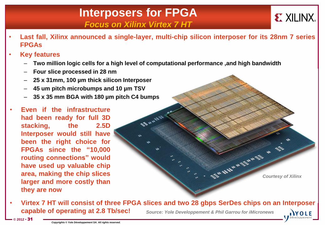
Interposers for FPGA Focus on Xilinx Virtex 7 HT
• Last fall, Xilinx announced a single-layer, multi-chip silicon interposer for its 28nm 7 series
FPGAs
• Key features
– Two million logic cells for a high level of computational performance ,and high bandwidth
– Four slice processed in 28 nm
– 25 x 31mm, 100 µm thick silicon Interposer
– 45 um pitch microbumps and 10 µm TSV
– 35 x 35 mm BGA with 180 µm pitch C4 bumps
• Even if the infrastructure
had been ready for full 3D
stacking, the 2.5D
Interposer would still have
been the right choice for
FPGAs since the “10,000
routing connections” would
have used up valuable chip
area, making the chip slices
larger and more costly than
they are now
• Virtex 7 HT will consist of three FPGA slices and two 28 gbps SerDes chips on an Interposer
capable of operating at 2.8 Tb/sec!
Source: Yole Developpement & Phil Garrou for iMicronews
Courtesy of Xilinx
© 2012 • 32
Copyrights © Yole Développement SA. All rights reserved.
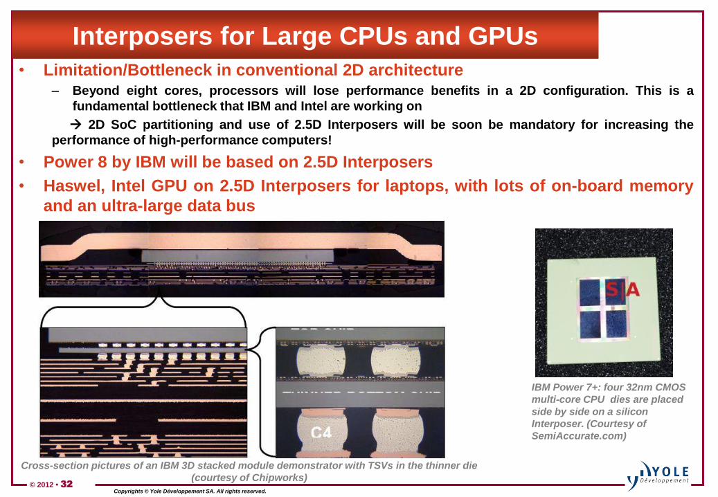
Interposers for Large CPUs and GPUs
• Limitation/Bottleneck in conventional 2D architecture – Beyond eight cores, processors will lose performance benefits in a 2D configuration. This is a
fundamental bottleneck that IBM and Intel are working on
2D SoC partitioning and use of 2.5D Interposers will be soon be mandatory for increasing the
performance of high-performance computers!
• Power 8 by IBM will be based on 2.5D Interposers
• Haswel, Intel GPU on 2.5D Interposers for laptops, with lots of on-board memory
and an ultra-large data bus
IBM Power 7+: four 32nm CMOS
multi-core CPU dies are placed
side by side on a silicon
Interposer. (Courtesy of
SemiAccurate.com)
Cross-section pictures of an IBM 3D stacked module demonstrator with TSVs in the thinner die
(courtesy of Chipworks)
© 2012 • 33
Copyrights © Yole Développement SA. All rights reserved.
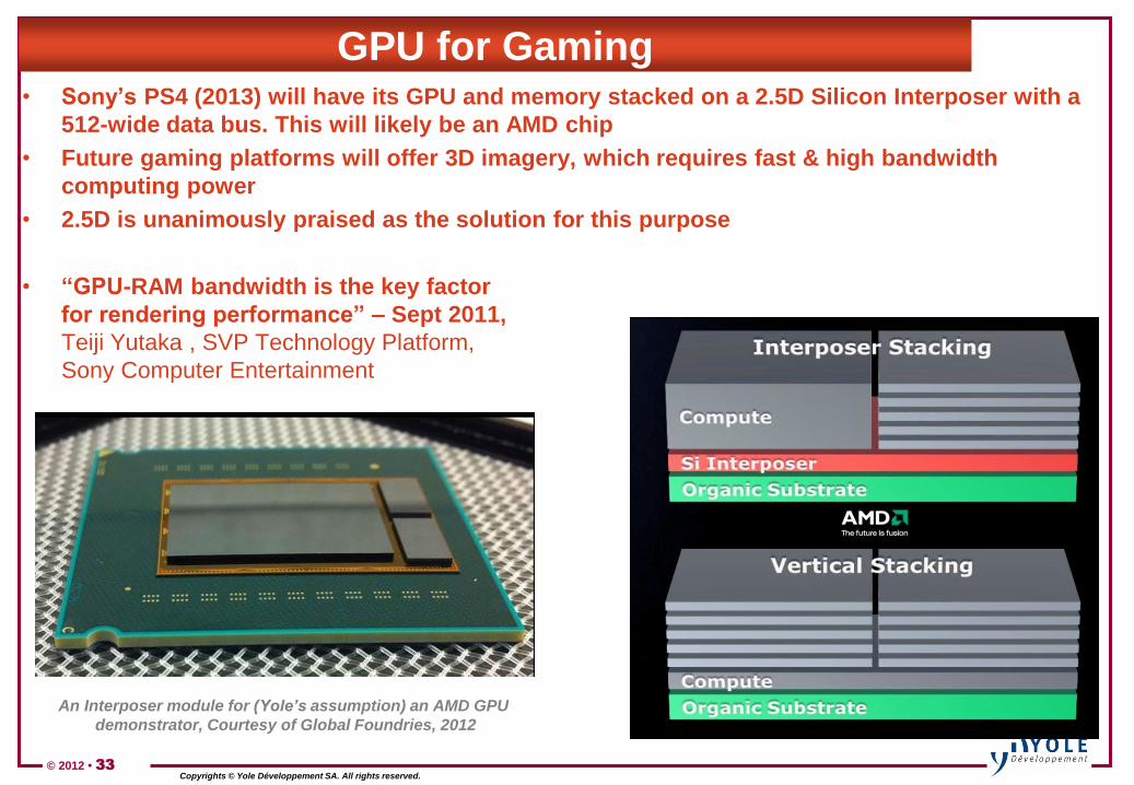
GPU for Gaming • Sony‟s PS4 (2013) will have its GPU and memory stacked on a 2.5D Silicon Interposer with a
512-wide data bus. This will likely be an AMD chip
• Future gaming platforms will offer 3D imagery, which requires fast & high bandwidth
computing power
• 2.5D is unanimously praised as the solution for this purpose
• “GPU-RAM bandwidth is the key factor
for rendering performance” – Sept 2011,
Teiji Yutaka , SVP Technology Platform,
Sony Computer Entertainment
An Interposer module for (Yole’s assumption) an AMD GPU
demonstrator, Courtesy of Global Foundries, 2012
© 2012 • 34
Copyrights © Yole Développement SA. All rights reserved.
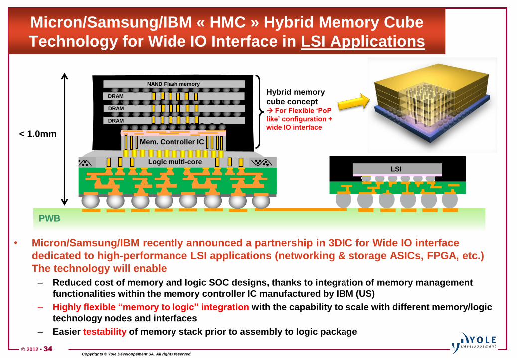
Micron/Samsung/IBM « HMC » Hybrid Memory Cube
Technology for Wide IO Interface in LSI Applications
• Micron/Samsung/IBM recently announced a partnership in 3DIC for Wide IO interface
dedicated to high-performance LSI applications (networking & storage ASICs, FPGA, etc.)
The technology will enable
– Reduced cost of memory and logic SOC designs, thanks to integration of memory management
functionalities within the memory controller IC manufactured by IBM (US)
– Highly flexible “memory to logic” integration with the capability to scale with different memory/logic
technology nodes and interfaces
– Easier testability of memory stack prior to assembly to logic package
LSI
PWB
Logic multi-core
< 1.0mm
DRAM
NAND Flash memory
DRAM
DRAM
Mem. Controller IC
Hybrid memory
cube concept For Flexible „PoP
like‟ configuration +
wide IO interface
© 2012
Copyrights © Yole Developpement SA. All rights reserved.
Conclusions &
Perspectives
© 2012 • 36
Copyrights © Yole Developpement SA. All rights reserved.
Main Conclusions and Perspectives
• 3DIC technology is considered today as a new paradigm for the future of the semiconductor
industry!
– 3DIC will enable several more decades of chip evolution at ever lower cost, higher performance and
smaller-size features
• 3D stacked DRAM and 3D Logic SOC applications are expected to be the biggest drivers for
the volume adoption of 3DIC technology in the next five years, followed by CMOS image
sensors, power devices and MEMS
– Today, the market is driven by high-end applications using 2.5D partitioning Interposers
– Large-die FPGAs and ASICs are on the way to being commercialized for industrial applications, and
are also expected to grow in the near future in the gaming and smart TV markets
• 2013 will likely be the key turning point for the first true implementation of 3DIC technology
in significant volume, driven by the commercialization of hybrid memory cubes
• In terms of value, the 3D TSV market will reach $40B in 2017, growing more than 10 times
faster than the global semiconductor industry!
– Looking closer at the Interposer industry -- as of 2017, Yole expects 2.5D Interposer revenues to
attain 14% of the packaging substrate market value
– 3D WLCSP is the preferred solution today for the efficient assembly of small-size optoelectronic
chips like CMOS image sensors. It is also the most mature 3D TSV platform at the moment, as we
estimate the market to be ~ $270M in 2011 for the “middle-end” processing factories serving this
specific market
© 2012 • 37
Copyrights © Yole Developpement SA. All rights reserved.
Find Out More…
About our company: www.yole.fr
About these markets: www.i-micronews.com


