25
TSV in IC Packaging: Now and Future Mike Ma, Ph.D. Vice President, SPIL
TSV in IC Packaging: Now and Future
Mike Ma, Ph.D.
Vice President, SPIL
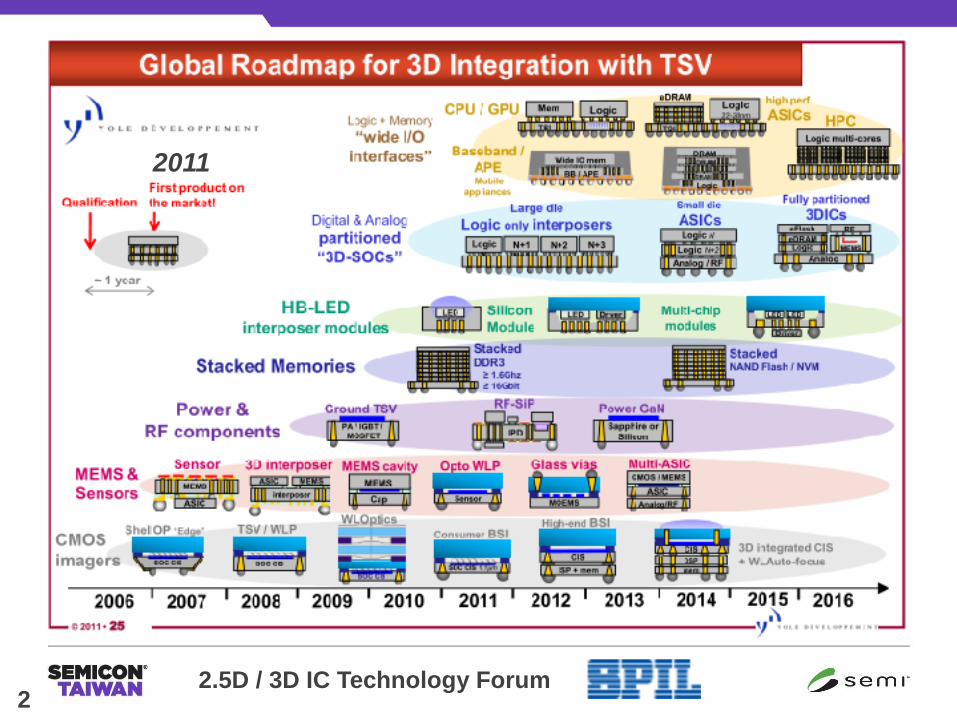
2.5D / 3D IC Technology Forum 2
2011
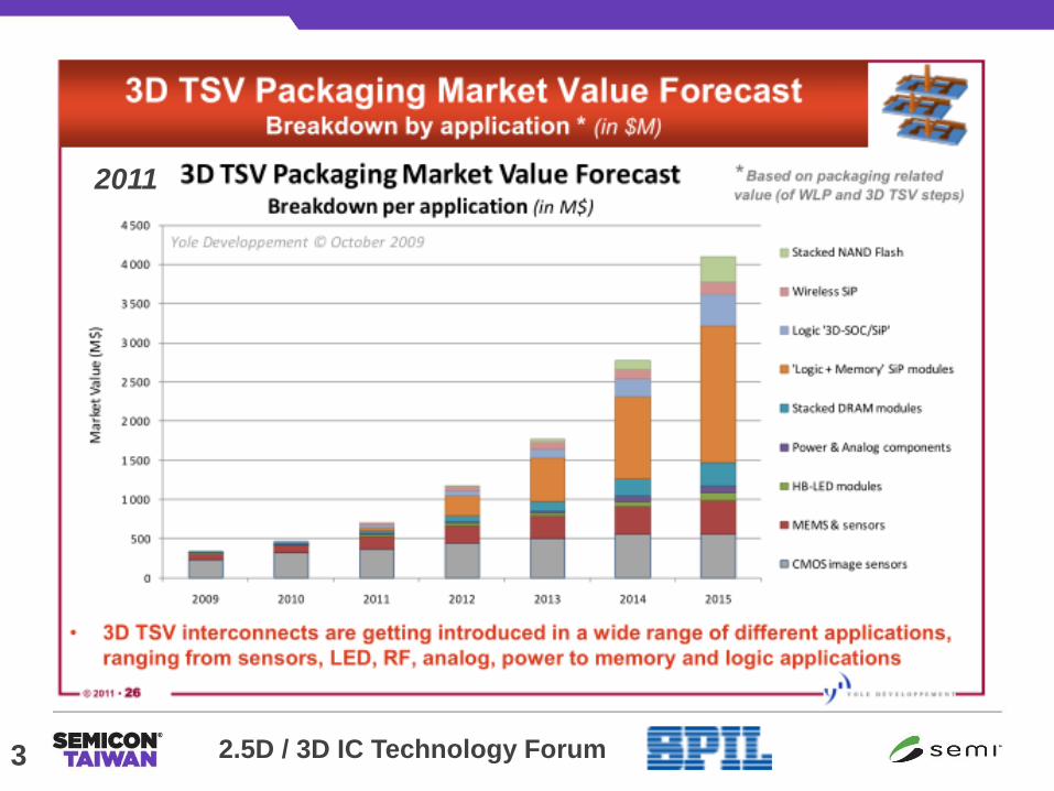
2.5D / 3D IC Technology Forum 3
2011
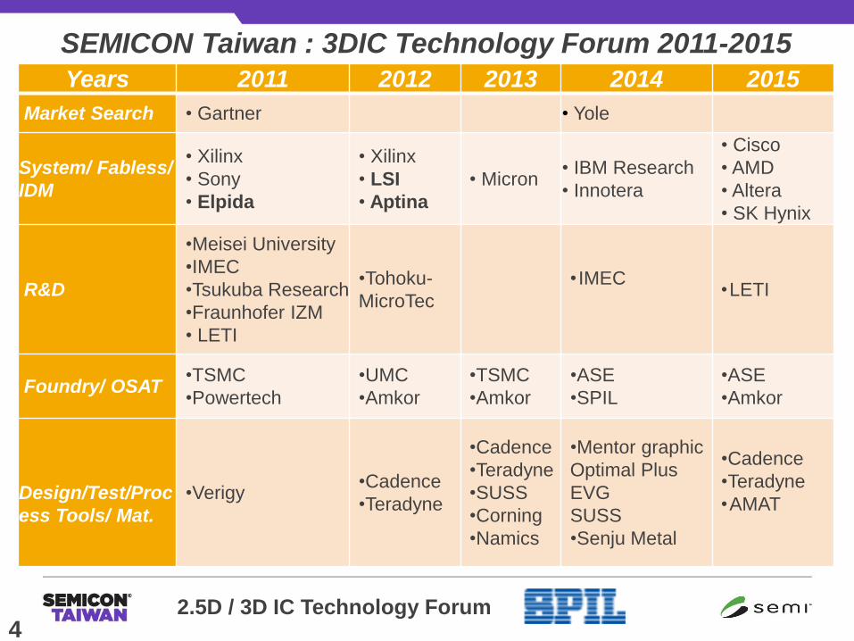
2.5D / 3D IC Technology Forum 4
Years 2011 2012 2013 2014 2015
Market Search • Gartner • Yole
System/ Fabless/
IDM
• Xilinx
• Sony
• Elpida
• Xilinx
• LSI
• Aptina
• Micron • IBM Research
• Innotera
• Cisco
• AMD
• Altera
• SK Hynix
R&D
•Meisei University
•IMEC
•Tsukuba Research
•Fraunhofer IZM
• LETI
•Tohoku-
MicroTec
• IMEC
•LETI
Foundry/ OSAT •TSMC
•Powertech
•UMC
•Amkor
•TSMC
•Amkor
•ASE
•SPIL
•ASE
•Amkor
Design/Test/Proc
ess Tools/ Mat.
•Verigy •Cadence
•Teradyne
•Cadence
•Teradyne
•SUSS
•Corning
•Namics
•Mentor graphic
Optimal Plus
EVG
SUSS
•Senju Metal
•Cadence
•Teradyne
•AMAT
SEMICON Taiwan : 3DIC Technology Forum 2011-2015

2.5D / 3D IC Technology Forum 5
So what’s Through Si Via (TSV) 3DIC/ 2.5DIC Adoption Status
1. TSV in CIS : Sony..
2. Low cost TSV in MEMS/Sensor
3. 3D IC with TSV: only in High Band Width (HBM) DRAM
Hynix, Samsung start HBM-1 LVM in 2015
HBM-2 in 2016
Advantage proven, cost still high
4. 2.5D IC with TSV Si Interposer
Nov. 2010 Xilinx debuted 1st product group (FPGA)
May. 2015: AMD rolled out 2nd product group (GPU+HBM)
June. 2016 nVidia GP100 with HBM-2
Renew interests for high end networking, VR/AR
2.5D / 3D IC Technology Forum
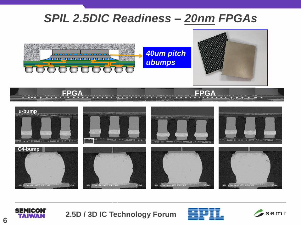
SPIL 2.5DIC Readiness – 20nm FPGAs
FPGA FPGA
C4-bump
u-bump
6
40um pitch
ubumps
2.5D / 3D IC Technology Forum
Micro joint C4 joint
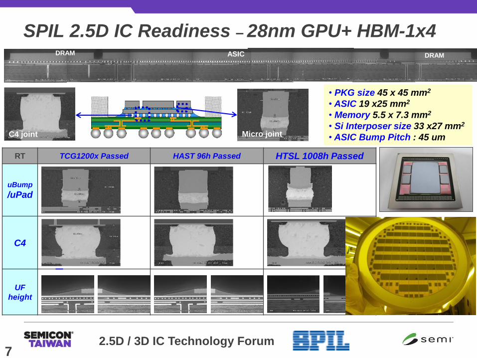
SPIL 2.5D IC Readiness – 28nm GPU+ HBM-1x4
• PKG size 45 x 45 mm2
• ASIC 19 x25 mm2
• Memory 5.5 x 7.3 mm2
• Si Interposer size 33 x27 mm2
• ASIC Bump Pitch : 45 um
ASIC DRAM DRAM
RT TCG1200x Passed HAST 96h Passed HTSL 1008h Passed
uBump
/uPad
C4
UF
height
7
2.5D / 3D IC Technology Forum
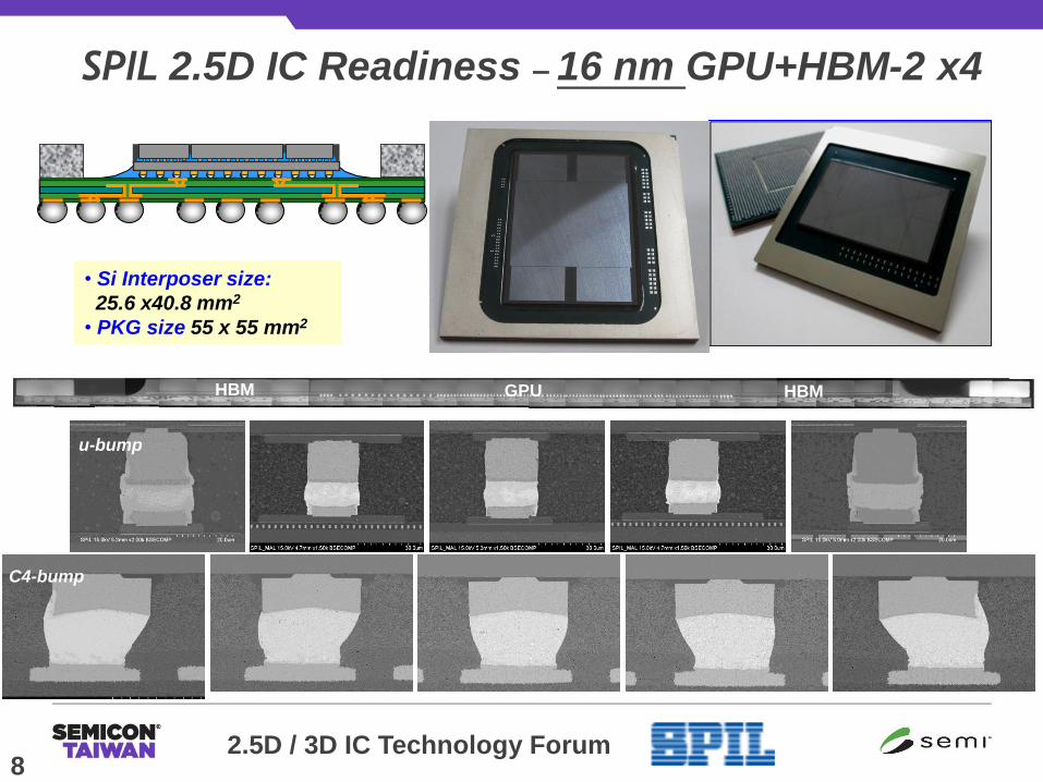
SPIL 2.5D IC Readiness – 16 nm GPU+HBM-2 x4
8
GPU HBM HBM
Cu pillar bump
u-bump
C4-bump
• Si Interposer size:
25.6 x40.8 mm2
• PKG size 55 x 55 mm2
2.5D / 3D IC Technology Forum
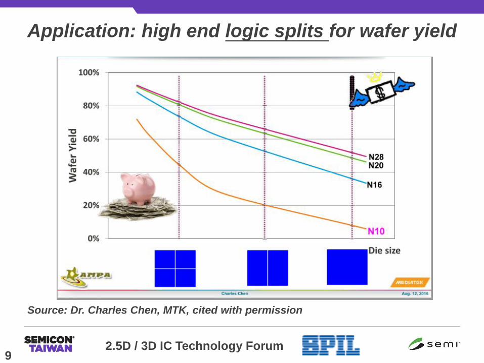
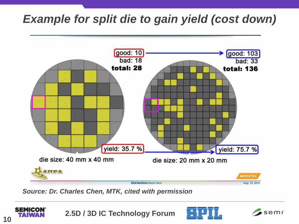
Application: high end logic splits for wafer yield
9
Source: Dr. Charles Chen, MTK, cited with permission
2.5D / 3D IC Technology Forum
Example for split die to gain yield (cost down)
10
Source: Dr. Charles Chen, MTK, cited with permission
2.5D / 3D IC Technology Forum
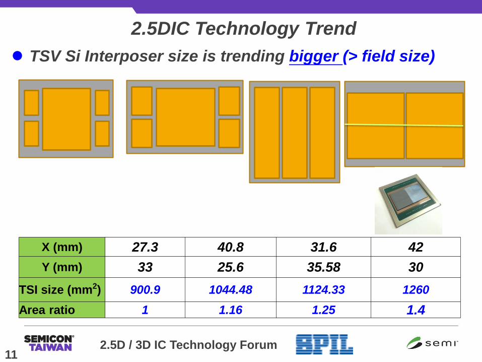
2.5DIC Technology Trend
X (mm) 27.3 40.8 31.6 42
Y (mm) 33 25.6 35.58 30
TSI size (mm2) 900.9 1044.48 1124.33 1260
Area ratio 1 1.16 1.25 1.4
11
TSV Si Interposer size is trending bigger (> field size)
2.5D / 3D IC Technology Forum
2011
2.5D / 3D IC Technology Forum 13
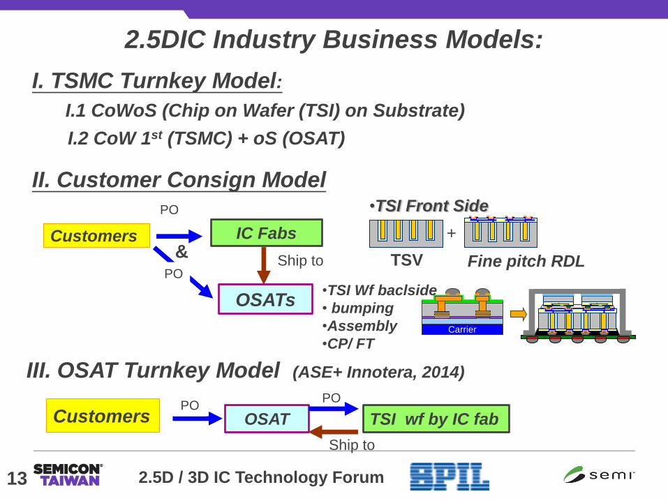
2.5DIC Industry Business Models:
III. OSAT Turnkey Model (ASE+ Innotera, 2014)
Carrier
•TSI Front Side
TSV
+
Fine pitch RDL
•TSI Wf baclside
• bumping
•Assembly
•CP/ FT
& Customers IC Fabs
PO
OSATs
Ship to
Customers OSAT TSI wf by IC fab PO
PO
Ship to
I. TSMC Turnkey Model:
I.1 CoWoS (Chip on Wafer (TSI) on Substrate)
I.2 CoW 1st (TSMC) + oS (OSAT)
II. Customer Consign Model PO
2.5D / 3D IC Technology Forum
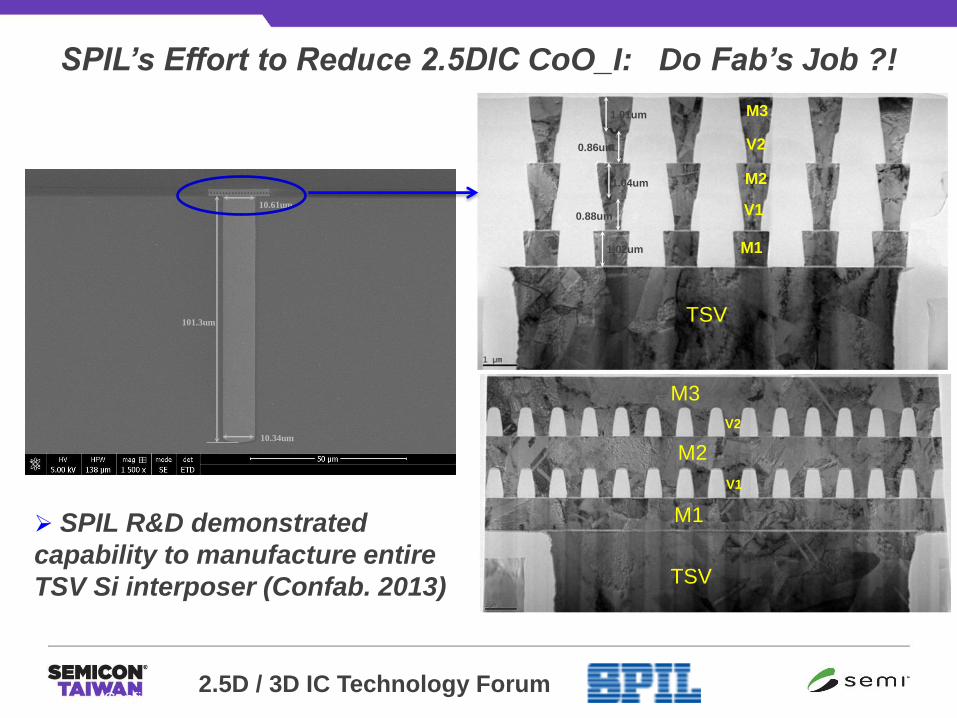
SPIL R&D demonstrated
capability to manufacture entire
TSV Si interposer (Confab. 2013)
SPIL’s Effort to Reduce 2.5DIC CoO_I: Do Fab’s Job ?!
14
Confidential
101.3um
10.34um
10.61um
1.0um
0.9um
1.0um
TSV
M1
V1
M2
V2
M3
TSV
M1
M2
M3
V1
V2
1.04um
0.88um
1.02um
0.86um
1.01um
2.5D / 3D IC Technology Forum
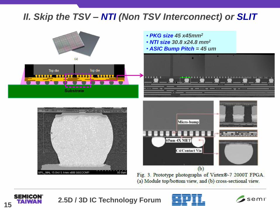
II. Skip the TSV – NTI (Non TSV Interconnect) or SLIT
15
• PKG size 45 x45mm2
• NTI size 30.8 x24.8 mm2
• ASIC Bump Pitch = 45 um
2.5D / 3D IC Technology Forum
Top Die
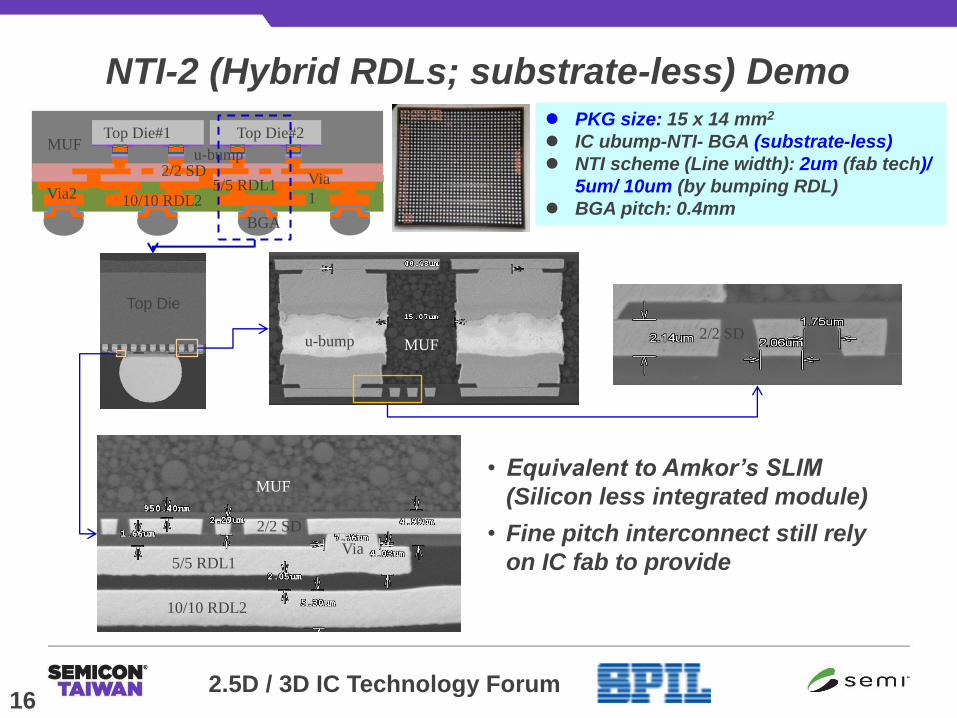
NTI-2 (Hybrid RDLs; substrate-less) Demo
16
PKG size: 15 x 14 mm2
IC ubump-NTI- BGA (substrate-less)
NTI scheme (Line width): 2um (fab tech)/
5um/ 10um (by bumping RDL)
BGA pitch: 0.4mm
2/2 SD 5/5 RDL1
10/10 RDL2
u-bump
Top Die#2
BGA
Top Die#1 MUF
Via
1 Via2
2/2 SD
2/2 SD
5/5 RDL1
10/10 RDL2
Via
MUF
u-bump MUF
• Equivalent to Amkor’s SLIM
(Silicon less integrated module)
• Fine pitch interconnect still rely
on IC fab to provide
2.5D / 3D IC Technology Forum
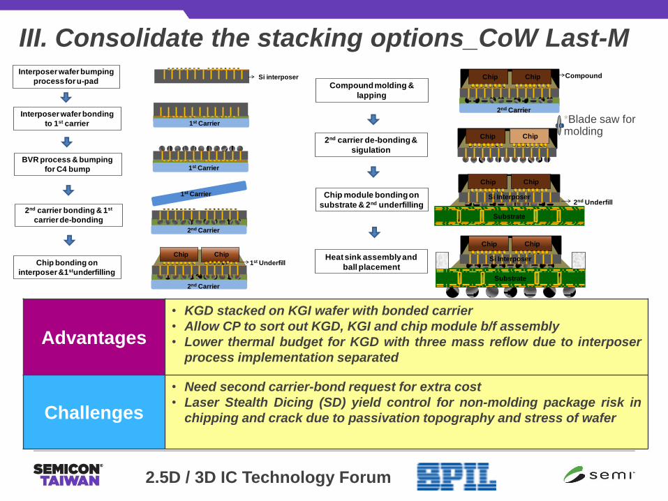
III. Consolidate the stacking options_CoW Last-M Interposer wafer bumping
process for u-pad
Chip bonding on
interposer &1stunderfilling
Compound molding &
lapping
Interposer wafer bonding
to 1st carrier
BVR process & bumping
for C4 bump
Heat sink assembly and
ball placement
2nd carrier de-bonding &
sigulation
2nd carrier bonding & 1st
carrier de-bonding
Si interposer
1st Carrier
ChipChip
Chip Chip
Substrate
Si Interposer
Chip Chip
Substrate
Si Interposer2nd Underfill
1st Carrier
2nd Carrier
1st Carrier
ChipChip
2nd Carrier
1st Underfill
ChipChip
2nd Carrier
Compound
Chip module bonding on
substrate & 2nd underfilling
Interposer wafer bumping
process for u-pad
Chip bonding on
interposer &1stunderfilling
Compound molding &
lapping
Interposer wafer bonding
to 1st carrier
BVR process & bumping
for C4 bump
Heat sink assembly and
ball placement
2nd carrier de-bonding &
sigulation
2nd carrier bonding & 1st
carrier de-bonding
Si interposer
1st Carrier
ChipChip
Chip Chip
Substrate
Si Interposer
Chip Chip
Substrate
Si Interposer2nd Underfill
1st Carrier
2nd Carrier
1st Carrier
ChipChip
2nd Carrier
1st Underfill
ChipChip
2nd Carrier
Compound
Chip module bonding on
substrate & 2nd underfilling
*Blade saw for molding
Advantages
• KGD stacked on KGI wafer with bonded carrier
• Allow CP to sort out KGD, KGI and chip module b/f assembly
• Lower thermal budget for KGD with three mass reflow due to interposer
process implementation separated
Challenges
• Need second carrier-bond request for extra cost
• Laser Stealth Dicing (SD) yield control for non-molding package risk in
chipping and crack due to passivation topography and stress of wafer
2.5D / 3D IC Technology Forum
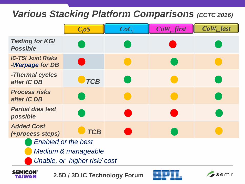
Various Stacking Platform Comparisons (ECTC 2016)
CoCi CioS CoWi_first CoWi_last
Testing for KGI
Possible
IC-TSI Joint Risks
-Warpage for DB
-Thermal cycles
after IC DB
Process risks
after IC DB
Partial dies test
possible
Added Cost
(+process steps)
TCB
Enabled or the best
Medium & manageable
Unable, or higher risk/ cost
TCB

2.5D / 3D IC Technology Forum
Status of Contenders of TSV Si Interposer (2.5DIC)
Si Interposer has unparalleled ‘Fine Pitch (<1 um) line
and via ‘ capability and suitable for high density
multiple die packaging
• Other close contender status are:
• Glass Interposer : came and gone, lack of ecosystem
• Organic Interposer (fine line laminated substrate):
delivery of 5um line keep delaying, cost still unknown;
PCB industry need to invest below 5um
• Fan Out Packaging: capability of 2um line x 2 layers
demonstrated, but larger package size (> 15 x 15 mm2)
will be challenging
19
2.5D / 3D IC Technology Forum
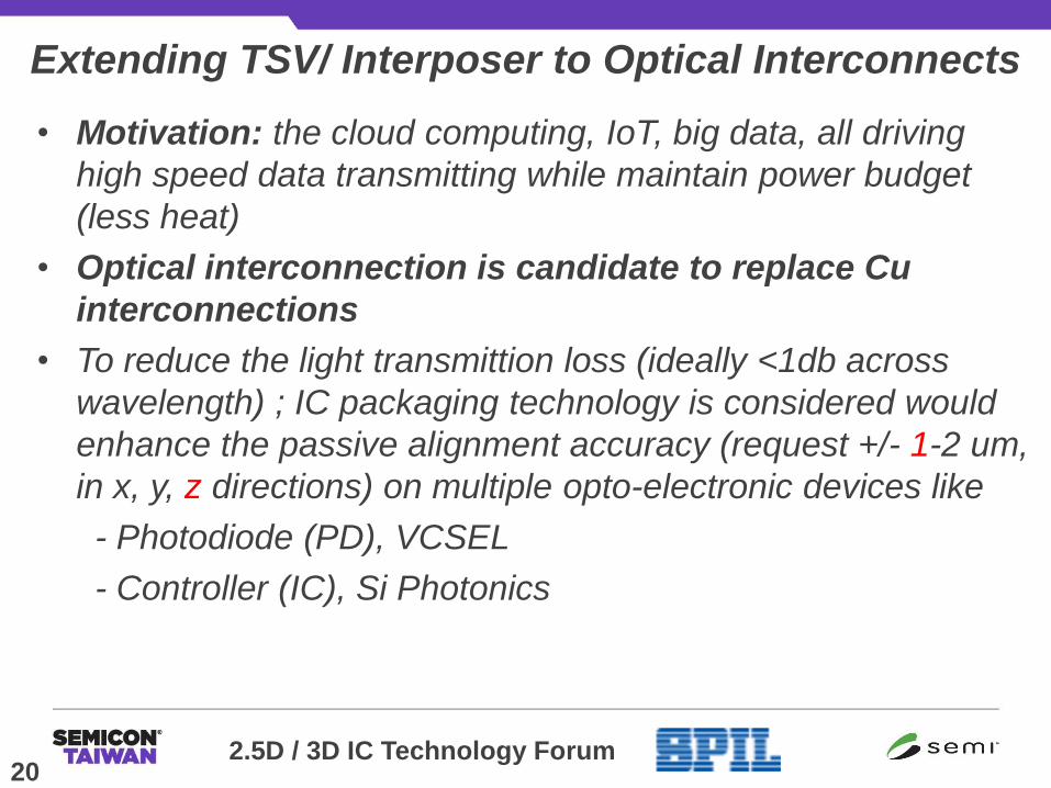
Extending TSV/ Interposer to Optical Interconnects
• Motivation: the cloud computing, IoT, big data, all driving
high speed data transmitting while maintain power budget
(less heat)
• Optical interconnection is candidate to replace Cu
interconnections
• To reduce the light transmittion loss (ideally <1db across
wavelength) ; IC packaging technology is considered would
enhance the passive alignment accuracy (request +/- 1-2 um,
in x, y, z directions) on multiple opto-electronic devices like
- Photodiode (PD), VCSEL
- Controller (IC), Si Photonics
20
21 2.5D / 3D IC Technology Forum
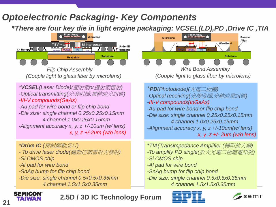
Optoelectronic Packaging- Key Components
21
*There are four key die in light engine packaging: VCSEL(LD),PD ,Drive IC ,TIA
Flip Chip Assembly
(Couple light to glass fiber by microlens)
Wire Bond Assembly
(Couple light to glass fiber by microlens)
*VCSEL(Laser Diode)(面射型or邊射型雷射)
-Optical transmitting(光發射端,電轉成光訊號)
-III-V compounds(GaAs)
-Au pad for wire bond or flip chip bond
-Die size: single channel 0.25x0.25x0.15mm
4 channel 1.0x0.25x0.15mm
-Alignment accuracy x, y, z +/-10um (w/ lens)
x, y, z +/-2um (w/o lens)
*PD(Photodiode)(光電二極體)
-Optical receiving(光接收端,光轉成電訊號)
-III-V compounds(InGaAs)
-Au pad for wire bond or flip chip bond
-Die size: single channel 0.25x0.25x0.15mm
4 channel 1.0x0.25x0.15mm
-Alignment accuracy x, y, z +/-10um(w/ lens)
x, y ,z +/- 2um (w/o lens)
*Drive IC (雷射驅動晶片)
- To drive laser diode(驅動控制雷射光發射)
-Si CMOS chip
-Al pad for wire bond
-SnAg bump for flip chip bond
-Die size: single channel 0.5x0.5x0.35mm
4 channel 1.5x1.5x0.35mm
*TIA(Transimpedance Amplifier (轉阻放大器)
-To amplify PD single(放大光電二極體電訊號)
-Si CMOS chip
-Al pad for wire bond
-SnAg bump for flip chip bond
-Die size: single channel 0.5x0.5x0.35mm
4 channel 1.5x1.5x0.35mm
Si Interposer
Substrate
Underfill
HermeticVCSELDrive IC PD TIAC4 Bump
TSV
Fiber ArrayMicrolens
Heat sinkSubstrate
VCSELDrive TIA
Fiber ArrayMicrolens
PD
Wire Bond
Passive
Align
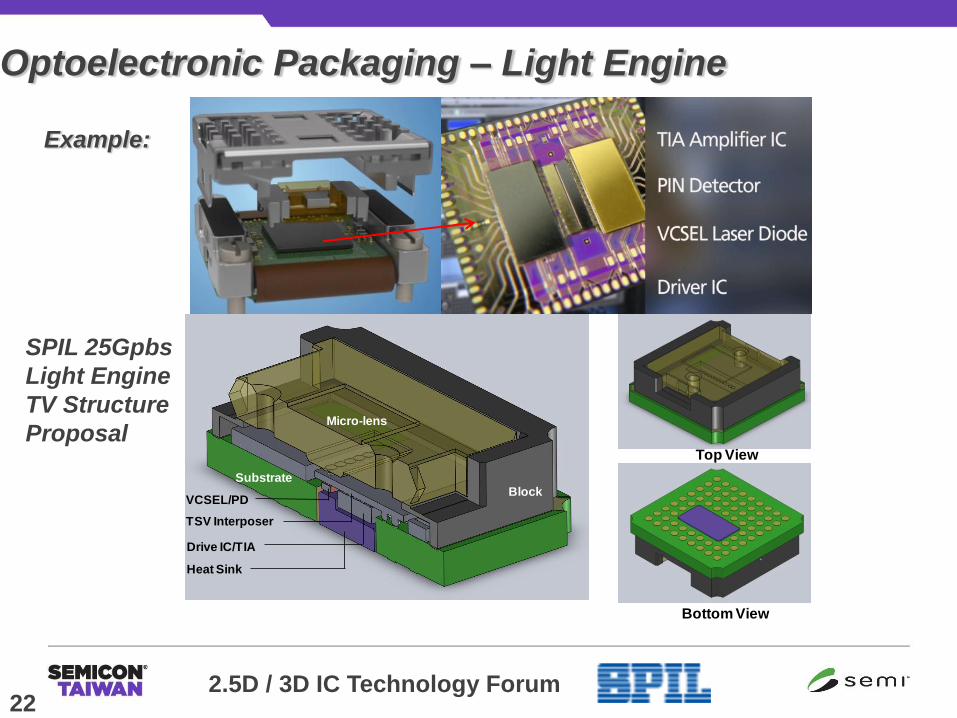
22 2.5D / 3D IC Technology Forum
Optoelectronic Packaging – Light Engine
SPIL 25Gpbs
Light Engine
TV Structure
Proposal Top View
Bottom View
Block
Micro-lens
Substrate
TSV Interposer
Drive IC/TIA
VCSEL/PD
Heat Sink
Example:
2.5D / 3D IC Technology Forum 23
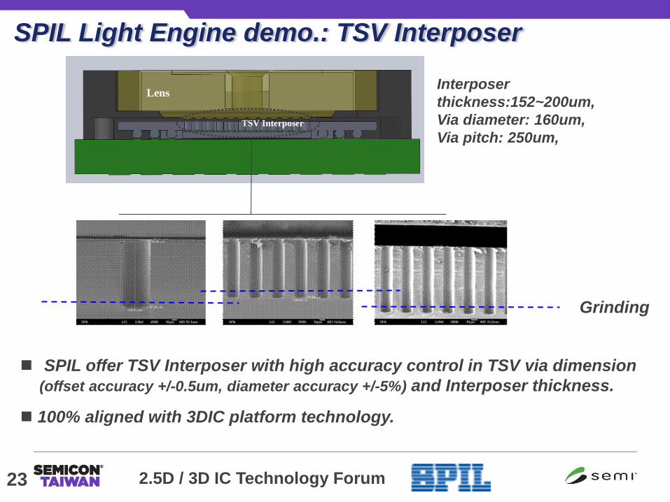
SPIL offer TSV Interposer with high accuracy control in TSV via dimension
(offset accuracy +/-0.5um, diameter accuracy +/-5%) and Interposer thickness.
100% aligned with 3DIC platform technology.
Interposer
thickness:152~200um,
Via diameter: 160um,
Via pitch: 250um,
Grinding
Small bump Small bump
TSV Interposer
Lens
SPIL Light Engine demo.: TSV Interposer
24 2.5D / 3D IC Technology Forum
Confidential 24
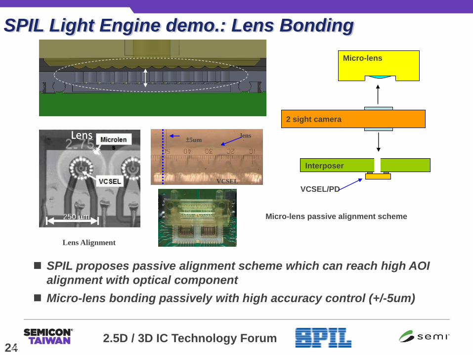
Micro-Lens
±5um
VCSEL
lens
Lens Alignment
Lens Lens
Micro-lens passive alignment scheme
Micro-Lens
Interposer
2 sight camera
Interposer
VCSEL/PD
Micro-lens
SPIL Light Engine demo.: Lens Bonding
SPIL proposes passive alignment scheme which can reach high AOI
alignment with optical component
Micro-lens bonding passively with high accuracy control (+/-5um)
2.5D / 3D IC Technology Forum
Summary:
• TSV 3DIC is realized in high bandwidth memory (HBM),
TSV Si interposer (2.5DIC) have been adopted that
realized the homogeneous and heterogeneous
integration
• High cost due to fragmented supply chain still limited
2.5DIC in very high end products that can afford it
• The ramping of 2.5DIC will largely depending on the
speed of cost down and how fast the other contending
alternatives can close in with better C/P value
• TSV interposer can also be applied in optoelectronic
packaging, but depending on the structure and it is not
a must be solution
25


