4. CMOS Transistor Theory Jacob Abraham Department of Electrical and Computer Engineering The University of Texas at Austin VLSI Design Fall 2019 September 10, 2019 ECE Department, University of Texas at Austin Lecture 4. CMOS Transistor Theory Jacob Abraham, September 10, 2019 1 / 31
Transcript
4. CMOS Transistor Theory
Jacob Abraham
Department of Electrical and Computer EngineeringThe University of Texas at Austin
VLSI DesignFall 2019
September 10, 2019
ECE Department, University of Texas at Austin Lecture 4. CMOS Transistor Theory Jacob Abraham, September 10, 2019 1 / 31
Electrical Properties
Necessary to understand basic electrical properties of the MOStransistor to design useful circuits
Deal with non-ideal devices
Ensure that the circuits are robust
Create working layouts
Predict delays and power consumption
As circuit dimensionsscale down, electricaleffects become moreimportant, even fordigital circuits
1.65 GHz square wavefrom an HDMI Interface
(Source: Dunnihoo, EE
Times Asia, 8/25/2005)
ECE Department, University of Texas at Austin Lecture 4. CMOS Transistor Theory Jacob Abraham, September 10, 2019 1 / 31
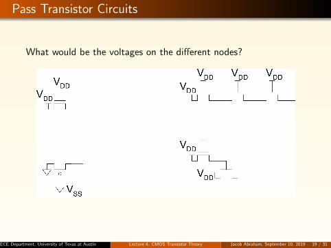
The nMOS Transistor
Terminal Voltages
Modes of operation depend on Vg, Vd, VsVgs = Vg − VsVgd = Vg − VdVds = Vd − Vs = Vgs − Vgd
Source and drain are symmetric diffusion terminals
By convention, source is terminal at lower voltage, so Vds ≥ 0
nMOS body is grounded for simple designs; assume source is 0
Three regions of operation: Cutoff, Linear, Saturated
ECE Department, University of Texas at Austin Lecture 4. CMOS Transistor Theory Jacob Abraham, September 10, 2019 2 / 31
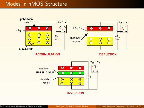
Modes in nMOS Structure
ECE Department, University of Texas at Austin Lecture 4. CMOS Transistor Theory Jacob Abraham, September 10, 2019 3 / 31
nMOS Transistor Operation
Positive voltage on Gate produces electric field across substrate –attracts electrons to the Gate and repels holes
With sufficient voltage, region under Gate changes from p- ton-Type – conducting path between the Source and Drain
Inversion layer is field-induced junction, unlike a PN junctionwhich is metallurgical
Horizontal component of electric field associated with Vds > 0is responsible for sweeping electrons from channel to drain
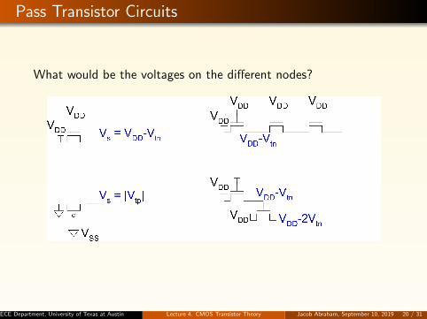
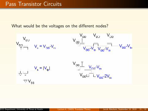
Threshold Voltage
The gate voltage at which conduction takes place is theThreshold Voltage, Vt
Current flow occurs when the drain to source voltage Vds > 0,and consists almost entirely of majority-carriers (electrons),that flow through the channel
A depletion region insulates the channel from the substrateECE Department, University of Texas at Austin Lecture 4. CMOS Transistor Theory Jacob Abraham, September 10, 2019 4 / 31
Conducting nMOS Transistor
Conduction when Vgs > Vt and Vds > 0No significant current through the substrate because of reversebiased PN junction with the channelAs the voltage from drain to source is increased, the resistivedrop along the channel begins to change the shape of thechannel characteristicAt source end of the channel, the full gate voltage is effectivein inverting the channelAt drain end of the channel, only the difference between thegate and the drain voltage is effective
If Vds > Vgs − Vt, then Vgd < Vt, and the channel is “pincheddown” (the inversion layer no longer reaches the drain)
In this case, conduction is brought about by the driftmechanism of electrons under the influence of positive drainvoltage; as the negative electrons leave the channel, they areaccelerated towards the drain
Voltage across the pinchdown channel tends to remain fixedat (Vgs − Vt), and the channel current remains constant withincreasing Vds
ECE Department, University of Texas at Austin Lecture 4. CMOS Transistor Theory Jacob Abraham, September 10, 2019 5 / 31
nMOS Device Behavior
Vgs > Vt, Vds = 0
Saturated Mode(Vds > Vgs − Vt)
Nonsaturated ModeVds < Vgs − Vt
ECE Department, University of Texas at Austin Lecture 4. CMOS Transistor Theory Jacob Abraham, September 10, 2019 6 / 31
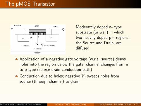
The pMOS Transistor
Moderately doped n- typesubstrate (or well) in whichtwo heavily doped p+ regions,the Source and Drain, arediffused
Application of a negative gate voltage (w.r.t. source) drawsholes into the region below the gate; channel changes from nto p-type (source-drain conduction path)
Conduction due to holes; negative Vd sweeps holes fromsource (through channel) to drain
ECE Department, University of Texas at Austin Lecture 4. CMOS Transistor Theory Jacob Abraham, September 10, 2019 7 / 31
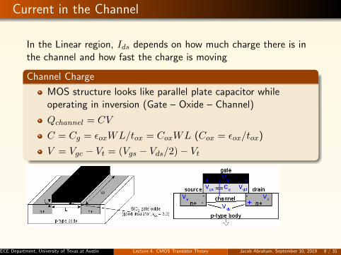
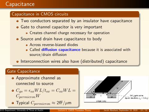
Current in the Channel
In the Linear region, Ids depends on how much charge there is inthe channel and how fast the charge is moving
Channel Charge
MOS structure looks like parallel plate capacitor whileoperating in inversion (Gate – Oxide – Channel)
Qchannel = CV
C = Cg = εoxWL/tox = CoxWL (Cox = εox/tox)
V = Vgc − Vt = (Vgs − Vds/2)− Vt
ECE Department, University of Texas at Austin Lecture 4. CMOS Transistor Theory Jacob Abraham, September 10, 2019 8 / 31
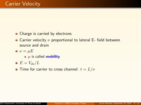
Carrier Velocity
Charge is carried by electrons
Carrier velocity ν proportional to lateral E- field betweensource and drain
ν = µE
µ is called mobility
E = Vds/L
Time for carrier to cross channel: t = L/ν
ECE Department, University of Texas at Austin Lecture 4. CMOS Transistor Theory Jacob Abraham, September 10, 2019 9 / 31
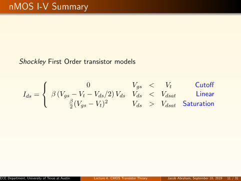
I-V Characteristics
nMOS Linear I-V
Current can be obtained from charge in channel and the time teach carrier takes to cross
Ids =Qchannel
t
= µCoxW
L(Vgs − Vt − Vds/2)Vds
= β (Vgs − Vt − Vds/2)Vds
nMOS Saturation I-V
If Vgd < Vt, channel pinches off near drain
when Vds > Vdsat = Vgs − VtNow drain voltage no longer increases with current
Ids = β (Vgs − Vt − Vdsat/2)Vdsat
=β
2(Vgs − Vt)2
ECE Department, University of Texas at Austin Lecture 4. CMOS Transistor Theory Jacob Abraham, September 10, 2019 10 / 31